METHOD FOR FAULT LOCALIZATION IN CIRCUITS
CROSS REFERENCE TO RELATED APPLICATION
This patent application claims the benefit of copending U.S. Provisional Patent Application, Serial Number 60/480184, filed 06/20/2003, entitled "FAULT LOCALIZATION USING TIME RESOLVED PHOTON EMISSION AND SIMULATED WAVEFORMS," by Desplats et al.
BACKGROUND
FIELD
The present writing generally relates to fault localization. More particularly, the present writing relates to the field of using measured time resolved photon emission data and simulated time resolved photon emission data for fault localization.
RELATED ART
When a device (e.g., an electronic device, an integrated circuit chip, etc.) is not operating correctly, a tester (e.g., automated test equipment (ATE)) can identify faults due to a wide range of sources (e.g., short circuits). To use a tester's capabilities to investigate defects, the minimum information required is a test sequence, which places the device in a failed mode and, therefore, the circuit in question in a failed mode. If the defect is more subtle, other solutions such as software based fault isolation may be used. With fault dictionaries and simulations, a greater range of defects may be covered but significant CPU time is required. When software diagnosis is insufficient (e.g., an incomplete fault model), fault isolation then requires the use of probes. Internal probing of a device can establish a measurement at specific nodes yielding valuable information concerning the actual behavior
of a circuit, both analog and digital. Existing techniques include: contact micro-probing, photon emission microscopy (PEM), electron beam probing, laser voltage probing and optical time resolved probing (e.g., time resolved photon emission (TRPE) and picoseconds imaging circuit analysis (PICA)). This latter technique makes it possible to measure precise optical waveforms through the backside silicon in order to obtain timing (e.g., signal delay) information.
To locate defects using these internal measurements, each waveform obtained must be compared with a known reference. This comparative approach works between two circuits (one good, one failed) or with regards to simulated signals. If simulation is used to obtain reference signals, the question that arises is "How to compare time resolved photo emission (TRPE) waveforms (linked with current) to logic state waveforms (linked with voltage)?"
SUMMARY
Methods for using measured time resolved photon emission data and simulated time resolved photon emission data for fault localization are provided and described. In one embodiment, a method of localizing a fault in a circuit includes generating simulation data based on logical states of the circuit at predetermined intervals. Moreover, the simulation data is converted into simulation photon emission data based on photon emission intensity of the circuit at the predetermined intervals. The simulation photon emission data is used in a fault localization technique.
In another embodiment, a method of localizing a fault in a circuit includes measuring photon emission from the circuit during a test time period to form photon emission data. The measurement is repeated a plurality of test cycles. Further, the photon emission data is digitized. The digitized photon emission data is converted into measured photon emission data based on photon emission intensity of the circuit at predetermined intervals. The measured photon emission data is used in a fault localization technique.
In yet another embodiment, a method of localizing a fault in a circuit includes generating simulation photon emission data for the circuit. Moreover, measured photon emission data for the circuit is generated. The simulation photon emission data is compared with the measured photon emission data to generate a comparison result. Further, the comparison result is classified according to predetermined criteria. The classified comparison result is used in a fault localization technique to determine next action in localizing the fault.
In still another embodiment, a method of localizing a fault in a plurality of circuits includes generating simulation photon emission data for each circuit. The simulation photon emission data of each circuit is merged into a composite simulation photon emission data.
Moreover, composite measured photon emission data for the circuits is generated. The composite simulation photon emission data is compared with the composite measured photon emission data to generate a comparison result. Further, the comparison result is classified according to predetermined criteria. The classified comparison result is used in a fault localization technique to determine next action in localizing the fault.
BRIEF DESCRIPTION OF THE DRAWINGS
The accompanying drawings, which are incorporated in and form a part of this specification, illustrate embodiments of the invention and, together with the description, serve to explain the principles of the present invention.
Figures 1-23 illustrate methods of localizing a fault in accordance with an embodiment of the present invention.
DETAILED DESCRIPTION
Reference will now be made in detail to embodiments of the present invention, examples of which are illustrated in the accompanying drawings. While the invention will be described in conjunction with these embodiments, it will be understood that they are not intended to limit the invention to these embodiments. On the contrary, the invention is intended to cover alternatives, modifications and equivalents, which may be included within the spirit and scope of the invention as defined by the appended claims. Furthermore, in the following detailed description of the present invention, numerous specific details are set forth in order to provide a thorough understanding of the present invention. However, it will be recognized by one of ordinary skill in the art that the present invention may be practiced without these specific details.
Software diagnosis makes it possible to investigate many IC defects with fault simulation tools. Faster defect localization can be achieved by combining IC simulations with internal measurements. Internal probing techniques, such as time resolved photon emission (e.g., TRPE), can access "otherwise inaccessible" nodes. Time resolved photon emission records photons emitted during commutations (current changes) rather than changes in logic states (voltage changes). These internal hardware diagnosis tools can fine- tune the defect analysis and validate simulations by contributing "actual" measurements. The combination of software diagnosis and internal probing can reduce simulation time and internal measurements for faster isolation of the root cause of a defect or fault. Comparing measured waveforms with simulations (e. g., Standard Test Interface Language (STIL) or Voltage Change Dump (VCD) formats) localizes functional faults and timing issues. The challenge is to determine quickly if an "actual" measurement is good or not: Can some signal be measured (Is the transistor at least activated)? Are the measured delays matching the simulation? If a problem is detected, the present invention makes it possible to locate rapidly the fault site.
Integrated circuit diagnostics (debug and failure analysis) and characterization employ several techniques— testing, software and internal probing (e.g., time resolved photon emission (TRPE)).
TRPE is a technique to capture photons that are emitted by transistor switching or commutation activity on an integrated circuit (IC) and to record the time of each photon relative to a trigger or timing reference signal. TRPE may incorporate either imaging (PICA) or single element type detectors. PICA is Picoseconds Imaging Circuit Analysis ( See J. A. Kash and J. C. Tsang, "Noninvasive Optical Method for Measuring Internal Switching and other Dynamic Parameters of CMOS Circuits", US Patent #5,940,545, issued August, 17, 1999). The PICA detector is an imaging type that records the time (t) and position (x, y) of individual photons. TRPE and PICA data, therefore, contain timing information useful in debug and failure analysis of integrated circuits and photon count, as illustrated by the graph 100 of Figure 1. The graph 100 shows two strong photon emission peaks and two weak photon emission peaks. A single element detector provides only timing data (t) from a local x, y region. A Photon Emission Microscope (PEM) camera records the position (x, y) of the sum of the optical emission from all switching events during the acquisition period.
Typically, test and validation of logic in a design is done using signals defined by voltage levels. A sequence of 0's and 1 's describe the input or output waveform for any points in a circuit. Internal probing of a device with either an e-beam prober or a laser voltage prober (LVP) makes it possible to measure the logic waveforms inside the device itself. Comparison of these measurements with simulation, for example, reveals disparities when a problem exists. However useful these tools are in general there are specific cases for which they do not work. E-beam probing requires physical access to the node being investigated (e.g., the metal interconnect). This is very challenging in present day integrated
circuits due to multiple levels of metallization and/or flip-chip packaging. Further the need to cool a flip chip package makes this completely unworkable through the silicon "back" side. The LVP is proving itself more useful than was believed several years ago, especially for timing measurements, but for silicon-on insulator (SOI) devices LVP has not been workable.
TRPE and PICA on the other hand record photons emitted due to current variation rather than changes in voltage logic states. The timing information obtained with TRPE and PICA while very precise is not compatible with existing testing tools. Histogram peaks (the optical waveforms) for some commutations are higher, i.e., contains more photons, than for other commutations and therefore are more readily classified. For example, a higher number of photons are collected from the NMOS transistor of an inverter whose output is switching from 1 to 0 than when it is switching from 0 to 1. For the PMOS transistor in the inverter, more photons are generated when the transistor switches from 0 to 1 than from 1 to O.
Photoemission from silicon devices such as an NMOS transistor that is pertinent to photon emission microscopy (PEM), TRPE and PICA is due to the generation of hot carriers, which have the highest probability of occurring when the transistor is switched ON via the VGS voltage and sufficient VDS is present while current is flowing through the channel to place the transistor in a saturation state, i.e., during commutation.
In addition to the substrate, an NMOS transistor has 3 nodes: gate G, drain D, and source S. From the electrical point of view, two quantities are considered— the gate to source voltage VGS and the drain to source voltage VDS. From a logic point of view, VGS and VDS are considered either logic 1 (>VT) or logic 0 (<VT). The threshold value Vτ comes from the circuit l-V curves illustrated in graph 200 of Figure 2.
Again, for the PMOS transistor photoemission from silicon devices that is pertinent to PEM, TRPE and PICA is due to the generation of hot carriers, as described for the NMOS transistor, i.e., during commutation. In addition to the substrate, a PMOS transistor also has 3 nodes: gate G, drain D, and source S. From the electrical point of view, two quantities are considered— the gate to source voltage VGS and the drain to source voltage VDS. In a typical CMOS device, a PMOS and NMOS pair forms the output stage in which drains of each device are electrically tied together. During logic switching operation, the possibility exists that both devices might be on for a brief moment resulting in photoemission from the NMOS via PMOS commutation activity. This is another mechanism by which photoemission from PMOS commutations can be observed.
As the voltage of ICs (integrated circuits) has decreased at each new process node, the signal that can be collected has also decreased. This means that the time to make a measurement has increased. Yet the number of transistors on a chip keeps increasing so the measurement time is growing exponentially. The PICA camera has poor photon detection (or quantum efficiency) when testing devices operating at low voltages (Vdd near 1 V). Other detectors used for TRPE are fairly exotic— InGaAs and super conducting Nb or NbN thin film based detectors. The cameras used for PEM are also getting more exotic— from silicon CCD's with thinned substrates to InGaAs, InSb, and MCT focal planar arrays (FPAs) and others. Even with the improved quantum efficiencies of these detectors, defect/fault localization is still challenging (design or process related) as the number of transistors increases on the IC chip, increased levels of metallization, smaller spacing, new materials, and increased transistor and interconnect density. The present invention decreases the time to make a decision in any localization technique utilized to localize the defect/fault.
Currently, there are several standards for voltage waveform simulations, such as STIL, VCD, Wave generation Language (WGL), etc. Previously, the transfer of data from simulation into the Automated Test Equipment (ATE) environment has been through the proprietary language of the specific ATE system. Value Change Dump (VCD) formats have been the typical way of capturing simulation output. The language is flexible enough to represent patterns from simple to the most complex devices, and has built in optimizing features to minimize the volume of data. VCD records every transition on each pin of the simulated device as a sequence of timed events and logic levels (1 's or 0's). This is fine for displaying a picture of the waveform, however it has limitations when used for creating test programs. VCD does not allow for any representation of the relation between events that is needed for any kind of analysis or characterization of the pattern from a real device. The VCD format requires an involved process to make the waveform/pattern realizable on most ATE systems which is usually done by means of expensive and time consuming conversion software.
In response to this issue and specifically to address growing concerns with large volumes of test data, an industry consortium of IC producers and ATE manufacturers came together to develop a Standard Test Interface Language (STIL) and is now part of standards committee (IEEE Std 1450.0-1999). STIL is designed to transfer high-density digital test patterns between simulation data created in Computer-Aided Engineering
(CAE) environments, automatic test pattern generation (ATPG) programs, built-in-self-test (BIST) data, and ATE equipment.
A tester (e.g., ATE equipment) is generally needed to activate the device while the probing tool acquires data. Converting ATE test vector data into a standard logic level format such as STIL provides a more efficient and easier means to review the data and
consequentially debug and characterize the device. The data conversion tools are generally part of the ATE tools suite.
While current simulation software tools have improved the methods of processing and displaying large volumes of data, the data is stored in logic level or voltage level formats which is not readily compatible with the data formats recorded by PEM, TRPE and PICA optical probing tools.
A discussion of prior art methods for fault localization may be found in U.S. Patent No.6,526,546 entitled "Method for locating faulty elements in an integrated circuit," issued February 25, 2003, which is hereby incorporated herein by reference.
SIMULATED AND MEASURED TIME RESOLVED PHOTON EMISSION DATA
Methods for using measured time resolved photon emission data and simulated time resolved photon emission data for fault localization are provided and described. In one embodiment, a method of localizing a fault in a circuit includes generating simulation data based on logical states of the circuit at predetermined intervals. Moreover, the simulation data is converted into simulation photon emission data based on photon emission intensity of the circuit at the predetermined intervals. The simulation photon emission data is used in a fault localization technique.
In another embodiment, a method of localizing a fault in a circuit includes measuring photon emission from the circuit during a test time period to form photon emission data. The measurement is repeated a plurality of test cycles. Further, the photon emission data is digitized. The digitized photon emission data is converted into measured photon emission
data based on photon emission intensity of the circuit at predetermined intervals. The measured photon emission data is used in a fault localization technique.
In yet another embodiment, a method of localizing a fault in a circuit includes generating simulation photon emission data for the circuit. Moreover, measured photon emission data for the circuit is generated. The simulation photon emission data is compared with the measured photon emission data to generate a comparison result. Further, the comparison result is classified according to predetermined criteria. The classified comparison result is used in a fault localization technique to determine next action in localizing the fault.
In still another embodiment, a method of localizing a fault in a plurality of circuits includes generating simulation photon emission data for each circuit. The simulation photon emission data of each circuit is merged into a composite simulation photon emission data. Moreover, composite measured photon emission data for the circuits is generated. The composite simulation photon emission data is compared with the composite measured photon emission data to generate a comparison result. Further, the comparison result is classified according to predetermined criteria. The classified comparison result is used in a fault localization technique to determine next action in localizing the fault.
In one aspect of the present invention, a method to compare the expected performance of the device— the simulations— to actual internal measurements from the device, for example the photon emissions/optical waveforms is provided. For example, the voltage/logic level simulation data generated by CAD/EDA tools can be exported in STIL, VCD or other useful data format which then can be converted into a photoemission compatible format such as a histogram indicating logic level transitions. This enables the fast localization of a discrepancy and therefore the identification of a design or process issue.
Once a design has been validated, any observed discrepancy would be a failure due to fabrication process issues, design marginality, or to misuse of the device.
Another aspect of the present invention is to provide the feedback from the "actual" measurements to the CAD/EDA models. For example, this might be performed by processing the actual photoemission data that can be in a histogram vs. time format and converted to a logic level format such as STIL, VCD or other useful data format by discerning which histogram transitions represent a 0 to 1 transition vs. a 1 to 0 transition. This is extremely valuable as it provides feedback to fine tune the models used by design.
In an embodiment of the present invention, simulated "optical waveforms" (or simulated time resolved photon emission data) are generated from simulated logic waveforms (typically in STIL or VCD format). Data processing is applied to correlate the simulated optical waveforms to actual optical waveforms (or measured time resolved photon emission data) with a minimum amount of real data as needed to provide sufficient confidence to determine the circuit to be functional or defective. The simulated logic waveforms providing the change of logic state information are used for generating the simulated optical waveforms. Also, in generating the simulated optical waveforms a variety of knowledge is used, where the knowledge can be the photon emission yield from a device which occurs due to a logic state change, which is a function of the transistor type (p or n channel), size, operating voltage, and fabrication process used.
Moreover, the invention enables the reconstruction of logic waveforms from PICA, TRPE and other optical waveform measurements. The invention may also be used in conjunction with the application of a differential laser voltage probing tool. An example of such a tool is described in U.S. Patent No. 6,252,222, entitled "Differential Pulsed Laser Probing of Integrated Circuits," issued June 26, 2001 , which is hereby incorporated herein
by reference. Further, the invention may be used with static photon emission. For example, simulated optical emission of a device can be performed. All emission events occurring during a specified period of time are added, yielding an expected cumulative emission height for that device which can be compared against actual static emission data. Although static photon emission would not show the waveforms it would tell, through peak height analysis, if the transistor is switching as would be appropriate for a properly functioning device.
This invention further includes a technique for faster fault localization that can be achieved by combining IC emission simulations with the internal optical probing measurements. The combination of simulation and internal probing of otherwise "inaccessible nodes" may be necessary to locate a fault in the heart of a device. Time resolved photoemission (TRPE) makes it possible to acquire precise timing waveforms corresponding to transistor commutations. A new data format is created, which contains simulated emission peaks (current levels). An example of this new data format is the
TRPEVCD (or TRPVCD) format or the TRPESTIL (or TRPs ) format. In one embodiment, the simulated emission in the new data format is derived from the logic "0" and "1 " simulation (voltage/logic levels) data, the transition points of the logic level data, and a scaling factor based on the specifics of the transistor as mentioned earlier. Actual TRPE measurements are acquired and converted into a TRPSTIL format or TRPVCD and compared to the simulated emission in order to generate a quick diagnosis: Is the gate working? Is there a timing issue? With a few measurements, the fault site can be located.
This invention further includes a method to rapidly decide whether a circuit node of a device is functioning correctly or not by defining a statistical confidence level as criteria to determine how many photons need to be collected to be statistically significant without
spending unnecessarily amount of acquisition time which otherwise does not add any relevance to the measurement.
Methods and apparatus for obtaining optical data for use in conjunction with the present invention may be found in U.S. Patent Application No. 10/234,231, entitled "Apparatus and Method for Detecting Photon Emissions from Transistors," filed 9/3/02, by Desplats et al., and in U.S. Patent Application entitled "Time-Resolved Optical Probing (PICA) with CAD Auto-Channeling for Faster IC Debugging," filed 12/5/02 by Desplats et. al., both of which are hereby incorporated herein by reference.
To convert 'Voltage/logic" information into a "current/emission" waveform, the electrical behavior of the circuit (e.g., transistor, logic gates, logic blocks, etc.) is needed. For the case of an NMOS transistor, all logic states and commutations are reviewed to understand the conditions for photoemission. From the static behavior (or truth table), a dynamic mode is built in order to show commutations and thus current/emission variations. Considering that photoemission is most probable when the transistor is switched ON via the VGS voltage and sufficient VDS is present while current is flowing through the channel to place the transistor in a saturation state, all transitions of VGS and VDS and expected emission are represented in a truth table 300 as illustrated in Figure 3. As depicted in truth table 300, these conditions are possible only in two cases 301 and 302, when the input VGS and the output VDS switch states from 0 to 1 and vice-versa.
Outside of switching in the CMOS architecture, saturation conditions occur only for a fault, as suggested in truth table 300 by "abnormal emission". Techniques such as lDDQ testing, Photon Emission Microscopy (PEM) and TLS (thermal laser stimulation) such as OBIRCH TΪVA/Seebeck Effect Imaging are often sufficient to locate the origin of these non- switching faults. In the TRPE analysis flow, the focus is on two possible emission peaks.
For initial illustration, the inverter is a good case. Further examples involve the analysis of the expected coverage of the truth table for CMOS structures such as NAND gates and XOR gates.
The invention may also be used with optically triggered devices such as those disclosed in U.S. Patent No. 6,501,288, entitled "On-Chip Optically Triggered Latch for IC Time Measurements," issued 12/31/2002, which is hereby incorporated herein by reference.
Again, as for the NMOS transistor, possible normal TRP emissions (or TRPE) occur only when both the input VGS and the output VDS of the transistor commutate in an opposite manner. For the inverter (Figure 4 shows a layout 410 and a schematic 420 of the inverter), all possibilities are determined from simulation 500 as depicted in Figure 5 and then listed in static truth table 610 and dynamic truth table 620 of Figure 6. The simulation 500 of Figure 5 shows voltage/logic state transitions in the input A and the output Y of the inverter of
Figure 4. Moreover, the simulation 500 depicts TRP emissions (or TRPE) associated with the NMOS 430 of the inverter of Figure 4. TRP emission (or TRPE) labeled #1 represents a strong photon emission peak while the TRP emission (or TRPE) labeled #2 represents a weak photon emission peak.
As depicted in Figure 6, TRP emission may happen only in two cases 631 and 632— when the inverter (Figure 4) is switching from 0 to 1 and vice-versa. The column labeled TNM0S displays TRP emissions for the NMOS Transistor 430 of the inverter (Figure 4) while the column labeled TPM0S displays TRP emissions for the PMOS Transistor 440 of the inverter (Figure 4). Moreover, the columns TNM0S and TPM0S indicate the type of TRP emission (e.g., #1 represents a strong photon emission peak, #2 represents a weak photon emission peak). In case 631 , the NMOS transistor 430 of the inverter (Figure 4)
generates a strong photon emission (shown as peak #1 in Figure 5) while the PMOS transistor 440 generates a weak photon emission. In case 632, the NMOS transistor 430 of the inverter (Figure 4) generates a weak photon emission (shown as peak #2 in Figure 5) while the PMOS transistor 440 generates a strong photon emission. For more complex gates such as NOR and NAND, this rule can be applied to create a dynamic truth table for TRP emissions.
To validate the functionality of a logic device, it is not necessary to cover all possible states. For the case of a NAND gate, the output may switch to 0 only if all inputs are at 1. As long as at least one input stays 0 it is not possible to validate the functionality of the NAND gate. (This is important as functionality can only be verified when all inputs are toggled high.) The truth table corresponds to all possible static state. Since photoemission in CMOS devices occurs only briefly during commutation, a dynamic truth table is necessary to cover the possible TRP emissions.
In Figure 7, the static truth table 700 for a variety of basic CMOS gates is shown. The static truth table 700 is derived to cover the different possibilities of photoemission (peak #1 or peak #2) for both NMOS and PMOS transistors.
For the NAND gate (Figure 8 shows a layout 810 and a schematic 820 of the
NAND gate), all possibilities of photoemission are determined from simulation 900 as depicted in Figure 9 and then listed in dynamic truth table 1000 of Figure 10. As shown in Figure 8, the schematic 820 of the NAND gate includes NMOS transistors 850 and 860 and includes PMOS transistors 830 and 840. The simulation 900 of Figure 9 shows voltage logic state transitions in the inputs A and B and voltage/logic state transitions in the output Y of the NAND gate of Figure 8. Moreover, the simulation 900 depicts TRP emissions (or TRPE) associated with the NMOS and PMOS transistors 830-860 of Figure
8, where TPA represents photon emissions by PMOS 840, TNA represents photon emissions by NMOS 850, TPB represents photon emissions by PMOS 830, and TNB represents photon emissions by NMOS 860. TRP emission (or TRPE) labeled #1 in TNB represents a strong photon emission peak while the TRP emission (or TRPE) labeled #2 in TNB represents a weak photon emission peak.
Symmetry is used to construct the dynamic truth table 1000 (Figure 10) for a NAND gate (Figure 8). The output Y is 1 if at least one input is 0 (see Figure 9). The dynamic truth table 1000 is limited to 6 (e.g., cases 1001-1006 of Figure 10) out of 16 possibilities: photon emission does not occur during the 4 static configurations, leaving 12 possibilities. Due to symmetry in the NAND gate (Figure 8), photon emission occurs in half the remaining commutations of the inputs (See Figure 10). In the dynamic truth table 1000 of Figure 10, the columns labeled TANMOS,TBNMOS, TAPM0S, and TBPM0S display TRP emissions for the transistors 850, 860, 840, and 830, respectively. Moreover, the columns TANM0S,TBNM0S, TAPMOg, and TBPMOg indicate the type of TRP emission (e.g., #1 represents a strong photon emission peak, #2 represents a weak photon emission peak).
For the NOR gate (Figure 11 shows a layout 1110 and a schematic 1120 of the NOR gate), all possibilities for photoemission are determined from simulation 1200 as depicted in Figure 12 and then listed in dynamic truth table 1300 of Figure 13. As shown in Figure 11 , the schematic 1120 of the NOR gate includes NMOS transistors 50 and 60 and includes PMOS transistors 30 and 40. The simulation 1200 of Figure 12 shows voltage/logic state transitions in the inputs A and B and voltage/logic state transitions in the output Y of the NOR gate of Figure 11. Moreover, the simulation 1200 depicts TRP emissions (or TRPE) associated with the NMOS and PMOS transistors 30-60 of Figure 11 , where TPA represents photon emissions by PMOS 40, TNA represents photon emissions by NMOS 60, TPB represents photon emissions by PMOS 30, and TNB
represents photon emissions by NMOS 50. TRP emission (or TRPE) labeled #1 in TNB represents a strong photon emission peak while the TRP emission (or TRPE) labeled #2 in TNB represents a weak photon emission peak.
The static table 700 of Figure 7 shows the NOR gate output is 0 if at least one input is 1. Therefore the interest is when all inputs commute to 1 and when at least one input switches to 0. This limits the dynamic truth table 1300 (Figure 13) to 6 cases 1301-1306 where photoemission occurs. In the dynamic truth table 1300 of Figure 13, the columns labeled TANM0S,TBNM0S, TAPM0S, and TBPM0S display TRP emissions for the transistors 60, 50, 40, and 30, respectively. Moreover, the columns TANM0S,TBNM0S, TAPM0S, and TBPM0S indicate the type of TRP emission (e.g., #1 represents a strong photon emission peak, #2 represents a weak photon emission peak). Plotting voltage variation as well as possible TRPE current peaks, the symmetry between n-transistors and p-transistors, is clear (see Figure 12). Only looking at the n-transistors, for each voltage change on the output, a possible emission peak is seen. It means that the possibility to transform the TRP emission peak into a state level exists.
The OR gate (Figure 14 shows a layout 1410 and a schematic 1420 of the OR gate) and AND gate (Figure 15 shows a layout 1510 and a schematic 1520 of the AND gate) are identical to the NOR and NAND gates (Figures 11 and 8, respectively) above except the output goes through an INVERTER at the final stage.
Increasing the gate complexity of CMOS structures to a 6 transistor XOR (Figure 16 shows a schematic 1620 of the XOR gate), its output is 0 if all inputs are identical. As for a NAND gate or NOR gate, TRP emission may be monitored on the n-transistors. By symmetry, the XNOR gate (Figure 17 shows a schematic 1720 of the NXOR gate) information is contained in the p-transistors.
Due to symmetry of logic gates in CMOS technology, probing n-transistors only can monitor the outputwaveform. Probing p-transistors yields the same results even though the photon emissions seem to be weaker and of longer wavelength. The coverage of the truth table is obtained only if all n-transistors connected to the output are probed. However, as a rule of thumb, a 2 input gate is probed at two locations and a 4 input gate at 4 locations. After this detailed review of the dynamic truth table, the role of "dynamic" emission peaks (current) versus "static" logic states (voltage) appears clear. For the NOR gate (Figure 11), as for example, there are 6 possible emission cases out of the 16 transitions while there is only 1 logic change out of 4.
As photoemission occurs only when a transistor switches (note: channel leakage does occur when the transistor is in the off state but is small in present technologies), only rise and fall of a logic state are discernable. In other words, the optical waveforms (e.g., TRPE) identify when a logic transition occurred. With the goal of reconstructing logic waveforms based on these emission peaks, it is necessary to see if it possible to differentiate emission from rising edges and emission from falling edges. Otherwise, reconstructing a logic state is difficult.
In previous paragraphs, emission peaks have been classified as #1 and #2 for both
N and P transistors. While these were represented differently for clarity purpose, the emission physics helps clarify what rising and falling transitions may be identified. Emission of photons associated with TRPE is related to hot electron generation occurring in the strong electron field during saturation. While photon emission is possible with hot holes, factors such as their lower mobility makes the probability much lower than for hot electrons. Comparison of emission peaks measured on NMOS and PMOS transistors of inverter chains shows a much higher photon count from N-transistors. Under the following
conditions: small size (e.g., 0.1 μm), low power (e.g., 1.2 V), photon emission detection technologies showed that photon counts from P-transistors are too close to the noise level to be consistent and therefore unreliable as a diagnostic tool. However, photon emission from the N-transistors also varies due to transistor load and, presumably, design-specific issues. For inverters, photon count rate for NMOS over PMOS is approximately 10 times higher when the output is switching from 1 to 0 (falling edge) than from 0 to 1 (rising edge). The graph 1800 of Figure 18 shows emission peaks for falling edges and rising edges. Therefore, logic state identification is possible.
Thus far, the conclusion is that the TRPE data may enable reconstruction of logic states. The problem arises is that if very few photons are detected for 0 to 1 (rising edge) commutations, it may always be possible to determine if a commutation occurred or that the few photons are just coming from the background noise. To capture the fainter P-transistor emissions with sufficient confidence level, acquisition time goes from minutes to several 10's of minutes. Acquisition times become even more discouraging as counts drop exponentially with the lower power supply voltage in new technologies.
Viewed from a practical approach, an alternative is needed— Can fault localization be done with short measurement times? This would not capture all rising commutations and thus leave uncertainty in 0 to 1 transitions.
To overcome this indetermination, a new data format for the Time Resolved Photon Emission is introduced to describe emissions (linked to a current) instead of a logic state (linked to a voltage level). This new data format is beneficial to any fault localization technique utilized. This new data format can be directly derived from logical (voltage) simulations.
Simulation logic waveforms are available in different industry standard formats such as Verilog-VCD, WGL, STIL, etc. The variety of formats has created duplicated effort for each vendor to interpret the format. In response to this issue and specifically to address growing concerns with large volumes of logic (voltage) test data, an industry consortium of IC manufacturers and ATE manufacturers came together to develop the Standard Test Interface language (STIL). For purpose of describing the present invention, reference is made to standard test vector data format, with the goal being to interface with the STIL vector data format specification. [Note: Verilog-VCD is an efficient way to dump value changes of variables in the design hierarchy and has been proved for performance and storage optimization.] In standard test data format, the series of logic states 0's and 1 's is stored to represent the voltage logic levels as Low (L) and High (H). From the photon emission perspective, only changes between logic states are meaningful. Therefore, in order to compare Time Resolved Photon Emission (or TRP emission) waveforms with simulations (STIL or VCD or other voltage-based waveforms), new data formats are introduced: TRPSTIL or TRPVCD. These new data formats represent commutation changes instead of logic states as seen in standard test vector data. An example of a test vector data for a simulation waveform converted to the simulation TRPSTIL format is shown in Figure 22.
As depicted in Figure 22, the STIL-formatted simulation data 110 is converted to simulation TRPSTIL data 120 (or simulation photon emission data). Since photon emission occurs during commutations, 1's are attributed to photon emission and 0's indicate no emission in simulation TRPSTIL data 120. With this terminology, TRPs 120 can be derived from logic/voltage STIL waveforms 110 and, further, the vice-versa is possible. To refine the Time Resolved Photon Emission, the lower probability of detecting photons for 0 to 1 commutations is addressed by adding a separate state value for the rising edge transitions on the output: "?/X" (for weaker photon emission peaks) while the falling edge has a state
value of 1 (for stronger photon emission peaks). From experimentation, the ratio between the peak for falling edge and the peak for rising edge is often greater than 10.
Thus, one embodiment of the TRPs format has 3 state values are possible: 0 (no TRPE emission); 1 (TRPE emission, falling edge); and "?/X" (Possible photon emission indicative of small rising edge peaks). In a second embodiment of the TRPSTIL format, the sub-threshold leakage current, which occurs when the transistor is 'off' is also taken into account. This added capability makes it possible to go beyond timing related faults and to tackle leakage problems, which grow in importance with each new process technology.
In one embodiment, time resolved photon emission probing, preferably from the backside, is used for measurements. That is, the photon emissions are detected with respect to a reference time. This technique makes it possible to measure precise signal waveforms through the silicon backside in order to obtain timing/delay information.
To locate defects/faults using internal probing, each measured waveform must be compared with a simulation logic waveform. To meet this goal, simulation logic waveforms (STIL or VCD format, for example) are first converted to the TRPSTIL format to serve as references for internal measurements and comparison.
Continuing, another step is to convert this photon emission measurement (analog waveform) into a waveform in the TRPST,L format. In a TRPE measurement instrument such as the NPTest IDS SSPD (Superconducting Single Photon Detector) or the IDS PICA system, the photon emission measurement (analog waveform) is digitized. In one embodiment, this digitization is done using a variable threshold with a Gaussian fit (Figure 20 shows digitization of analog photon emission measurement for a NOR gate), only the peaks are taken into account. However, the sub-threshold current variation can be taken into
account in order to increase the sensitivity to track subtle faults in the latest semiconductor technologies (e.g., size < 100 nm).
In Figure 19, the photon emission measurement for an NMOS device with the IDS SSPD system is shown. More specifically, logic (voltage) data 710, measured analog photon emission data 720, and digitized photon emission peaks 730 are depicted in Figure 19.
Moreover, in Figure 21 , the photon emission results for one N-transistor of a NOR gate is presented. More specifically, logic (voltage) data 41 , measured analog photon emission data 42, and expected digitized photon emission peaks 43 are depicted in Figure 21. In this case, not all weak photon emission peaks are detected. The reference 52 shows that a strong photon emission peak is detected while the reference 54 shows that a weak photon emission peak was not detected.
From the above discussion, it is evident that simulation TRPSTlL waveform can now be readily compared to the actual photon emission measurement from the internal node, generating a comparison result.
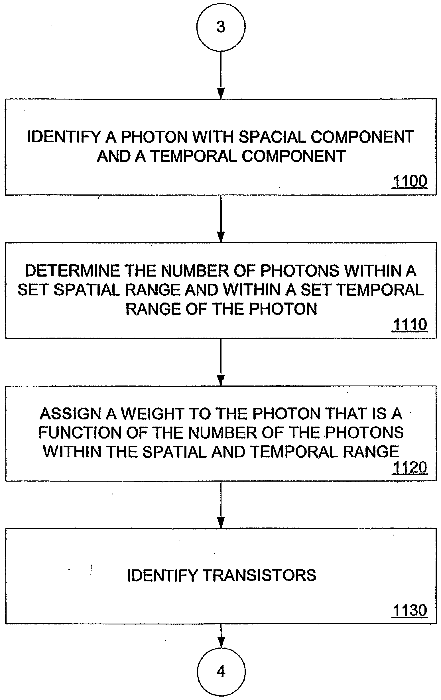
Now, a method for localizing a fault in a circuit (e.g., transistor, logic gates, logic blocks, etc.) that allows quick determination of fault origin in a device by combining logic simulation and optical measurements is presented. Reference is made to Figures 22 and 23.
At 2205 of Figure 22, simulation data 110 (e.g., simulation STIL-formatted data) based on logical states of the circuit at predetermined intervals is generated. Moreover, at 2215, the simulation data 110 is converted into simulation photon emission data 120 (e.g.,
simulation TRPSTIL format data) based on photon emission intensity of the circuit at the predetermined intervals.
Internal photon emission measurement (at 2220) may take several minutes to record a sufficient number of photons to become meaningful. As operating voltages decrease this time is expected to increase. Typically, the photon emission measurement is performed during a test time period. One test time period represents a test cycle. If an additional number of photons are to be measured, the test cycle is repeated as many times as needed.
At 2225, photon emission data 130 measured at 2220 is digitized. Moreover, the digitized photon emission data 140 is converted into measured photon emission data 150 (e.g., measured TRPSTIL format data) based on photon emission intensity of the circuit at predetermined intervals.
Continuing, at 2230, the simulation photon emission data 120 is compared with the measured photon emission data 150 to generate a comparison result. At 2235, the ■ comparison result is classified according to predetermined criteria. Further, the classified comparison result is used in the fault localization technique to determine next action in localizing the fault.
To locate quickly defects/faults with TRPE measurement and simulation, a strategy based on partially probed nodes is used. As shown in Figure 22, a 4 color coded diagnostic (e.g., Red, Orange, Yellow, and Green) has been chosen to guide the fault localization process, at 2235. Red and Orange correspond to detected faults (no commutation indicated by Red at 2255 or a delay problem indicated by Orange at 2250). At 2255, awareness of a major problem is made. At 2250, the next action in localizing the
fault is determined to be probing earlier in the propagation flow. At 2240, Green corresponds to the absence of faults (all measured commutations (e.g., measured TRPST,L) matching simulation (e.g., simulation TRPsτιl) and expected timing), allowing probing later in the propagation flow. Yellow corresponds to partially matching the measured commutations (e.g., measured TRPSTm) with the simulation (e.g., simulation TRPST(L) but, for at least the acquired peaks, the timing information seems to be correct, but may be incorrect for the missing peaks. At 2245, ft is determined that the photon emission measurement time needs to be increased. In the Yellow case, it may be assumed that the missing peaks are also correct, allowing the fault localization process to continue later in the propagation flow, at 2240. If a timing problem (Orange color) is then found, the last Yellow assumption must then be reconsidered. At this time only, a longer acquisition may be done, in order to verify the assumption made about the timing of the missing peak of the last Yellow assumption. Figure 23 illustrates the Green case 2320, the Yellow case 2310, the Orange case 2340, and the Red case 2330 of the 4 color coded diagnostic described above.
Further, at 2260, it is determined whether the fault has been localized. If not, a new measurement is performed at 2220. Otherwise, the fault localization process is ended at 2265.
To perform the fault localization technique as fast as possible, so as to probe as many points in the shortest amount of time, the following diagnostics questions are addressed:
1. Is Transistor On/Off (Is there a measured signal?)?;
2. Is Functionality validated (Is the data consistent with the logic gate being examined?)?; and
3. Is Delay/timing measurement accurate (Is there an issue here?)?
From the first minutes of measurement acquisition, the first diagnostic question is answerable—Is there a measured signal? If not, It means that the probed transistor is not activated. A major functional fault Is associated with this node. Probing nodes located earlier in the propagation flow will identify where the signal started to deteriorate.
if some photon emission is measured, the second diagnostic question concerning th validation of the unctional behavior is answerable. Is the number of measured commutations (photon emission peaks) matching the logic simulation? If not, probing earlier in the propagation flow is necessary to Isolate the fault site.
The third diagnostic question concerns timing and delay differences between measurement and simulation. If the margin is too great, probing earlier in the propagation flow to determine if the delay is coming from earlier gates is performed. If it is not coming from any earlier gate, the fault is due to an interconnect issue. If the timing of the measurements and simulation match, it means the fault is later in the propagation flow. In an embodiment, the determination of the next point to probe is done by following an extended binary search. With this strategy, at each measurement the number of remaining candidates is halved. If a sample of 512 nodes are potentially linked to a fault, the fault can be located after 8 measurements (28=512).
To speed fault localization, it is not always necessary to wait for a long acquisition to capture all commutations. Assuming the probed transistor is working, upon 2 out of 3 commutations are measured, the acquisition may be stopped. If later in the propagation flow a problem is found, it may be linked to the missing peak and a longer acquisition may then be necessary.
In an embodiment, the method for localizing faults described with respected to Figures 22 and 23 can be utilized to localize faults in a plurality of circuits rather than in a single circuit Here, simulation photon emission data (e.g., simulation TRPs ) for each circuit Is generated. The simulation photon emission data (e.g., simulation TRPδτlL) of each circuit Is merged into a composite simulation photon emission data. Composite measured photon emission data for tie circuits is generated since the plurality of circuits are measured at the same time. The composite simulation photon emission data is compared with the composite measured photon emission data to generate a comparison result. The comparison result is classified according to predetermined criteria. Further, the classified comparison result is used in a fault localization technique to determine next action in localizing the fault.
In an embodiment, the methods of the present invention are performed by computer-executable instructions stored in a computer-readable medium, such as a magnetic disk, CD-ROM, an optical medium, a floppy disk, a flexible disk, a hard disk, a magnetic tape, a RAM, a ROM, a PROM, an EPROM, a flash-EPROM, or any other medium from which a computer can read. The foregoing descriptions of specific embodiments of the present invention have been presented for purposes of illustration and description. They are not intended to be exhaustive or to limit the invention to the precise forms disclosed, and many modifications and variations are possible in light of the above teaching. The embodiments were chosen and described in order to best explain the principles of the invention and its practical application, to thereby enable others skilled in the art to best utilize the invention and various embodiments with various modifications as are suited to the particular use contemplated. It is intended that the scope, of the invention be defined by the Claims appended hereto and their equivalents.
As a broad summary, this writing discloses methods for using measured time resolved iphoton emission data and simulated time resolved photon emission data for fault localization, ϊa one embodiment, a method of localizing a fault in a circuit includes generating simulation photon emission data for the circuit. Moreover, measured photon emission data for the circuit is generated. The simulation photon emission data is compared with the measured photon emission data to generate a comparison result. Further, the comparison result is classified according to predetermined criteria. The classified comparison result is used in a fault localization technique to determine next action in localizing the fault.
This application is related to and claims the benefit of U.S. Patent Nos.6,526,546 (filed oh 25 February 2003), 6,501,288 (filed on 31 December 2002), 6,252,222 (filed on 26 June 2001), and to U.S. Patent Application No; 10/234,231 (filed on 03 September 2002), the entire contents, of which are hereby attached and expressly incorporated herein by this reference.
!(i2) ύn tec tates' atent (io) Patent No.: US 6,526,546 Bl
Holland et al. (45) Date of Patent: Feb.25, 2003
(54) METHOD FOR LOCATING FAULTY (56) References Cited
ELEMENTS IN AN INTEGRATED CmCϋlT U.S. PATENT DOCUMENTS
(75) Inventors: Guy Rolland, Escalquens (FR); 5,602,856 A 2 1997 Teramoto Remain Desplats, Toulouse (FR) FOREIGN PATENT DOCUMENTS
(73) Assignee: Centre National d'Etudes Spatiales, EP 0305217 3/1989 Paris (FR) EP 0720097 7/1996
OTHER PUBLICATIONS
( * ) Notice: Subject to any disclaimer, the term of this patent is extended or adjusted under 35 Stamenkoviό et al., May, 2000. International Conference On U.S.C. 154(b) by 0 days. MicToeletronics. pp. 735-738.*
(21) Appl. No.: 09/831,832 * cited by examiner
Primary Examiner— -Tom Thomas
(22) PCT Filed: Sep. 14, 2000 Assistant Examiner— -Douglas . Owens
(86) PCT No.: PCT FR00/02554 (74) Attorney, Agent, or Firm— Young & Thompson
§ 371 (c)(1), (57) ABSTRACT
(2), (4) Date: May IS, 2001 A process for locating defective elements in an integrated
(87) PCT Pub. No.: O01/20355 circuit. The integrated circuit is modelled in the form of a tree formed of nodes and oriented arcs. Measurements are PCT Pub. Date: Mar. 22, 2001 performed at various nodes of the circuit by applying a sequence of tests at the input of the circuit. The nodes to be
(30) Foreign Application Priority Data tested are determined recursively as a function of the result Sep. IS, 1999 (FR) 99 11534 of the tests previously performed. Each new test node is such that the number of its ancestors is substantially equal to the
(51) Int. Cl.7 G06F 17/50 number of its descendants.
(52) U.S. CI 716/4; 716/5
(58) Field of Search 716/4, 5, 6 9 Claims, 23 Drawing Sheets
Appendix A page 1 of 110
U.S. rateil '" "Feb 'S, 2 Sheet 1 of 23 ττ„
US 6,526,546 Bl
FIG.1
Appendix A page 2 of 110
.. eϋ , 3 Sheet 2 of 23 US 6,526,546 Bl
Appendix Apage 3 of 110
Sheet 3 of 23 US 6,526,546 Bl
Appendix A page 4 of 110
. , ee o , ,
FIG.3 FIG.4
Appendix A page 5 of 110
. . atent Feb.25, 2003 Sheet 5 of 23 US 6,526,546 Bl
FIG. 6 FIG. 7
FIG. 8A
Appendix A page 6 of 110
. . e . , ee o ZO tO JBl
Appendix A page 7 of 110
. * e . , ee o , ,
FIG 10
Appendix A page 8 of 110
. . eb.25, 2003 Sheet 8 of 23 US 6,526,546 Bl
FIG. 11
Appendix A page 9 of 110
e . , ee o
Appendix A page 10 of 110
Feb.25, 2003 Sheet 10 of 23 US 6,526,546 Bl
FIG. 13
Appendix A page 11 of 110
Reference tree
FIG. 15
.
CO
Appendix A page 13 of 110
.
Appendix A page 14 of 110
.o. ate I e. , eet o , ,
FIG.18
Appendix A page 15 of 110
e . , ee o 6,526,540 JS1
FIG. 19
Appendix A page 16 of 110
.O. raieil Feb. , 2003 Sheet 16 of 23 US 6,526,546 Bl
T=(Vertex~>counte ir_αncestors=<meαn)
FIG. 21
Appendix A page 17 of 110
U.S. Patent Feb.25, 2003 Sheet 17 of 23 US 6,526,546 Bl
Appendix A page 18 of 110
. . e . , eet o ,5 ,546 Bl
FIG.23
Appendix A page 19 of 110
ui e 5, Sheet 19 of 23 6,526,546 Bl
FIG. 24
Appendix A page 20 of 110
.
U.O. raten Feb.25, 2003 Sheet 20 of 23 US 6,526,546 Bl
FIG 25
Appendix A page 21 of 110
" . . n Feb.252003 Sheet 21 of 23 US 6,526,546 Bl
FIG.26
Appendix A page 22 of 110
. ateϊit Feb.25, 2003 Sheet 22 of 23 US 6,526,546 Bl
FIG 27
Appendix A page 23 of 110
. . e , ee o 6,526,546 J51
Appendix A page 24 of 110
U 6,526,54 B
METHOD FOR LOCATING FAULTY integrated circuit if the defective element is very close to an
ELEMENTS IN AN INTEGRATED CXRCUIT input of the circuit. Owing to the complexity of the circuits and their numerous constituent branches, the search for the
The present invention relates to a process for locating a defective element may prove to be extremely lengthy. defective element in an integrated circuit whose theoretical s The aim of the invention is to propose a process for layout is known, of the type comprising a succession of steps detecting errors in a circuit allowing faster locating of consisting in: defective zones, whilst preserving great reliability in this the determination of a measurement point of the inte- locating. 'grated circuit; and Accordingly, the subject of the invention is a process of the testing of the measurement point determined by 10 the aforesaid type, characterized in that it comprises iniimplementing: tially: the application of a sequence of tests to the inputs of the a step of modelling the theoretical layout of the integrated integrated circuit; circuit, in the form of at least one graph comprising a the measurement of signals at the determined measureset of nodes and of arcs oriented from the inputs of the ment point of the integrated circuit, during the applicircuit to the outputs of the circuit; cation of the sequence of tests; and is considering as a search subgraph, a subgraph whose the assessment of the measurement point by comparivertex-forming node corresponds to a faulty measureson of the measured signals with theoretical signals ment point , which ought to be obtained at the determined meaand in that, for the search for the defective element, it surement point so as to assess whether the measurecomprises the steps of: ment point is faulty or satisfactory; and 20 assigning each node of the search subgraph considered a in which the position of the defective element of the intecharacteristic variable dependent on the structure of the grated circuit is determined from assessments performed at search subgraph; the various determined measurement points. considering as measurement point the measurement point
It is expedient, in the manufacture of integrated circuits, or when searching for faults in industrial systems, to be able 25 corresponding to a node of the subgraph considered, to determine the origin of defects or breakdowns. obtained by applying a predetermined criterion pertain¬
In particular, in the case of defective integrated circuits, it ing to the characteristic variables of the set of nodes of is necessary to be able to determine which component or the search subgraph considered; performing a test of the measurement point considered; components constituting the integrated circuit exhibit an operating anomaly. 30 considering as new search subgraph: either the search subgraph previously considered,
The number of components involved in the construction while excluding the node corresponding to the of an integrated circuit is generally very high so that it is measurement point tested and all its parent nodes, very tricky to locate the one or the few defective elements if the measurement point is satisfactory from among the multitude of elements from which the breakdown may result. 35 or a subgraph whose node corresponding to the measurement point is the vertex, if the measure¬
Aprocess for analysing integrated circuits, known by the ment point is faulty; and English term "backtracking", is currently known. To implement this process, a testing rig is used, making it possible searching for the defective element in the new search with the aid of hardware or virtual probes to plot signals subgraph considered, until a predetermined stopping flowing at various circuit measurement points. 40 criterion is satisfied.
By knowing the theoretical structure of the integrated According to particular modes of implementation, the circuit analysed, the signals which ought to be measured at process comprises one or more of the following characterthe various circuit measurement points are determined as a istics: function of a sequence of tests applied to the inputs of the during the initial step of modelling the theoretical layout circuit. 45 of the integrated circuit, the circuit is modelled the form
In order to locate the defective elements in the circuit, a of a tree by possible creation of virtual nodes when one defective output of the circuit is first considered and then we and the same node is the parent of at least two nodes, backtrack from this output to the inputs, gradually testing themselves parents of one and the same node; each of the successive measurement points. As long as the it comprises, after satisfaction of the predetermined stopmeasurements performed at the various points reveal signals 50 ping criterion, the steps of: which are incorrect as compared with the theoretical signals evaluating in the or each last search subgraph whether, which ought to be obtained, one deduces that the defective for each virtual node corresponding to a faulty elements, of the circuit are upstream of the measurement measurement point, the twin node associated with point. As soon as correct signals are obtained at a measurethe said virtual node is a node of the same subgraph ment point, one deduces that the defective element is situ55 also corresponding to a faulty measurement point; ated between the measurement point where correct signals and are obtained and the previous measurement point where then considering the or each subgroup for which the incorrect measurement signals were obtained. condition is satisfied as corresponding to a part of the
Each measurement actually performed on the integrated integrated circuit comprising at least one defective circuit requires a considerable time which may range from element; a few seconds if the measurement point is at the surface to the said characteristic variable peculiar to each node is the 5 to 10 minutes if the measurement point is situated on a number of ancestors of this node in the search subgraph deep layer of the integrated circuit and if a prior hardware considered; port must be made with the aid, for example, of a focused ion the said predetermined criterion is suitable for determinbeam. 65 ing the node whose number of ancestors is substantially
It is appreciated that, with the method currently used, it is equal to the mean number of ancestors per node in the sometimes necessary to traverse back through the nub of the search subtree considered;
Appendix A page 25 of 110
Appendix A page 26 of 110
US 6,526,546 Bl
5 6
The program implemented by this rig makes it possible to The EDIF interpretation phase determine progressively, on the basis of the theoretical The marking phase diagram of an integrated circuit, the points where physical The numbering phase (this phase encompasses the con- measurements ought to be made by implementing a struction of the reference tree, the construction of the sequence of appropriate tests. 5 minimal subset and the creation of the virtual vertex)
After each acquisition of the result of the test performed The &ult location phase previously, making it possible to determine whether the The reporting phase, signal received at the measurement point is or is not correct, ^ calculations can be interru ted on completion of each the process implemented determines a new point where a of *e∞ P1""*- to cfe' aU * intermediate results
, , . . . . r - , ,, . . c r lo required for the subsequent resumption of the calculations tes ought to be performed on the basis of a new sequence automatically archived in save files. These files have of tests. names comprising a ".data" extension. The degree of
In tandem with the acquiring of the results of the auto- progress of the calculations is also archived, matically proposed tests, the process according to the inven- he calculations are resumed in a transparent manner, that tion makes it possible to locate that region of the integrated 1S is to say without having to make reference to these inter- circuit in which the defective element is situated and ulti- mediate files, by simply loading the appropriate session file, mately to locate the latter rapidly. Initially, the theoretical structure of the circuit, that is to
The test sequences implemented for each of the measure- sav &e structure of a defect-free circuit, is stored in a file ment points of the integrated circuit are of any suitable type 10*i ^ h e f<* βxamPk ^e EDIF format.
"backtracking^ process. Since the test sequences are known put -^ ^ foπn of m *mύ format sped&0 tø the per se, they will not be described in the subsequent descπp- implementation of the process. The manner of interpretation tion. ^ 102 and the format specific to the application of the process likewise, the means used to measure a signal at a ■will e described in the subsequent description, determined measurement point of the integrated circuit, 25 Generally, interpretation consists in modelling the theo- during the application of a sequence of tests will not be retical circuit in the form of a graph, whose nodes corre- described in detail, they being of any suitable type. spond to the inputs and to the outputs of the various
The process according to the invention can be imple- components of the integrated circuit and in which the mented with a rig comprising, on the one hand, test means components are represented by sets of oriented arcs inter- such as a scanning electron microscope making it possible to 30 linking the nodes. plot signals flowing at determined measurement points of The interpretation algorithm receives and addresses data the integrated circuit during the application of a sequence of to an internal session memory 104 catering in particular for tests, and, on the other hand, an information processing unit, temporary storage of the file containing the graph of the such as a microcomputer implementing a suitable program circuit presented according to a utilizable format, determining, in accordance with the process of the 35 This memory 104 is linked to a session file 106 catering invention, the points of the circuit where successive mea- for storage of the session data on a permanent medium such surements ought to be performed, and deducing from the as a hard disk. measurement results the position of the defective elements On completion of the interpretation 102, the session file is in the circuit. subjected to a marking phase 108 associated with other
Illustrated in FIG.1 are the various data files used as well 40 preliminary processing operations, as the processing operations performed on them, so as to The next phase denoted 110 is the so-called "minimal determine, on the one hand, the successive points where subset construction and numbering phase". Its aim is in measurements should be performed on the circuit and, on the particular to define subsets from among the various trees other hand, the defective elements or zones of the circuit. modelling the circuit. In particular, during phase 110, two
The general structure of the program implements the 45 series of information are taken into account, namely the list, session concept. denoted 112, of outputs of the circuit operating correctly, and
Asession can be defined as a set of consistent files relating the list, denoted 114, of outputs of the circuit not operating to given conditions for the inputs and the parameters of the correctly. Accordingly, the outputs of the circuit are tested on program. Asession also contains the set of intermediate files the basis of sequences of tests, as will be explained in the generated by the program, and which are necessary for 50 subsequent description. operations and for storing the number of the last calculation On the basis of the session file obtained at the output of step performed. step 110, a phase 116 of loading the lists is implemented.
The content of a session is defined in a text file whose This phase takes into account the list of disallowed nodes name bears the extension ".ses". The root of the name is stored in a file 118, the list of levels of metal 120 specifying defined freely by the user. 55 the metal layers on which the various elements of the circuit
The loading by the program of a preexisting session file are present, as well as a file 122 containing the list of nodes restores the calculation context specific to this session (same already tested. data files, same check parameters and intermediate results) The subsequent phase 123 consists in locating the defec- and enables the calculations to be restarted at the point tive components or groups of components causing faults in where they were interrupted. βo the operation of the circuit. According to the invention, this
The sequencing of the various operations is performed by search for faults is performed according to a dichotomy a function main( ). process effected with regard to certain particular trees of the
The code for this function is found in a file "principal.c". circuit, by taking account of a waiting also referred to as {he
According to the principle of the program, the various numbering of each of the nodes, performed according to a operations are chained together sequentially. 65 predetermined method.
Five main phases may be distinguished and will be During the dichotomy phase denoted 124, an additional detailed in what follows: analysis phase 126, the so-called "post-exhaustion analysis
Appendix A page 27 of 110
US 6,526,546 Bl
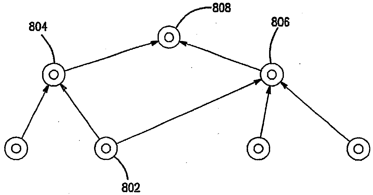
7 8 phase" is also implemented, this making it possible to Certain nodes are untestable nodes. These are for example supplement the dichotomy-based search for faults. This nodes situated on deep layers of the integrated circuit and to additional phase makes it possible to take account of the which access is impossible or difficult. These nodes are circuit modelling constraints which have led to certain designated by a nought inside which there is a question conventional modifications of the graph representing the 5 mark, circuit. The good nodes, as opposed to the bad nodes, are nodes
Finally, the results are made available to the user during where for a given sequence of tests, the measured signal the final phase 128. corresponds to the theoretical signal which ought to be
As represented in the schematic diagram, each of the obtained. These good nodes are designated by a nought processing phases 102, 108, 110, 116, 124, 126, 128 receives 10 inside which there is another nought, and addresses data from and to the internal session memory In the example of FIG.5, the faulty zone 500 consists of
104. The latter is moreover linked to a set of results files 130, a subtree whose vertex 502 is a bad node. This bad node 502 as well as to a storage journal 132. The latter respectively is controlled by two untestable nodes 503 and 504. The first ensure that the results of the analysis are made available to untestable node 503 is linked to two good nodes 506 and the user and ensure the archiving of the comments printed on 15 508. The second untestable node 504 is linked to a good the screen. node 510 and to an untestable node 512 itself linked to a
Each of the successive phases 102, 108, 110, 124 and 126 good node 514. for implementing the process according to the invention is In general, a subtree constituting a faulty zone has the described in greater detail in FIG. 2. following properties:
Thus, the detailed description of the full algorithm will be w The vertex is a node on which the signal is bad, performed with regard to FIG.2, where each of the elemen- All the terminations are nodes on which the signal is good tary steps will be described in succession with reference to Untestable nodes may exist between the vertex and the other yet more detailed illustrative figures. terminations. In the converse case, one is dealing with
The first step of the initial phase 102 for formatting the file a faulty cell or with faulty cells whose outputs are describing the integrated circuit is designated by the refer- 25 connected to the same node, ence 202 in FIG.2. An example of a faulty cell on its own is represented in
In general, a circuit can always be described as a set of HG. 6. An example of two faulty cells sharing the same cells comprising inputs and outputs connected by nodes. The output is described in FIG. 7. In these figures, the conven- choice of the hierarchical definition of a cell is arbitrary. It tions of FIG. 5 are used. may for example be a functional subset constituting a 30 τn practice, the interpretation step 202 consists in trans- macrocell, or be a gate or a transistor. Likewise, the concept forming the initial file describing the circuit, in the Edif of inputs and outputs of the circuit to be analysed can be format, for example, into a file of a. determined format immediately carried over to the inputs and outputs of an specific to the implementation of the process (file whose internal block, the. analysis then pertaining to this block. na e bears the suffix ".parsed").
With the type of description used, the signals are observed 35 According to the nature (tagged by one of the suffixes only on the nodes. ".edn", ".edf ' or ".edo") of the initial file, the program runs
The description of the cells reduces to the influence which the appropriate interpreter, their input nodes exert on their output nodes. The initial These interpretation programs are used as commands for circuit description formed of a set of cells and of nodes, can the operating system through the function "system( )" of the therefore be transformed into an inter-node influence graph 40 c language. by replacing each cell, an example of which is given in FIG. in the case where the initial description does not comply
3, by a set of oriented arcs such as illustrated in FIG.4. ^Jth the formats of the available interpreters, it is always
Represented in FIG.3 is a cell 300 consisting for example possible to make direct use of a description in the internal of an AND gate. This cell comprises two inputs El and E2 format (".parsed" format). linked to input nodes 302 and 304 respectively. These input 45 T e format of these internal files is given in Table 1. nodes are linked to the outputs of other cells (not T e conventional constraints to be adhered to are as represented) of the integrated circuit. The output, denoted S, follows: of the cell 300 is linked to a node 306 to which are linked It is a text file, the inputs of other cells (not represented) of the integrated - No ^ may be ^pp^
CU' ι Ui3r^-. Λ ιι inn - i j. «„ • . Λ ΛOΠ ° T e various blocks must be placed in the following order:
?!_?• ' ^"ϊ3^ repkcedby two oriented arcs 402 describing the outputs; the blocks de cribing and 404 respechvely linking the input nodes 302 and 304 to ^ ^s ^ ^^ j the output nodes 306 of the cell. .. . ,„„!„ J„_„,- J A. -,„Λ.„.
ThuJ the cellSOO is modelledsimplyby the two oriented e blocks describing the nodes, arcs 402 and 404 *■ •> J The numbering of the outputs commences at zero and
By virtue of such modelling of all the cells, the full terminates at N. description of the circuit thus takes the form of a graph. ^ numbering of the mputs commences at N+l and
Insuchamodeffingofthe circuitand asillustratedinFIG. terminates at (number_of_pιns-l) 5, a faulty zone 500 is a subgraph and even, after applying The numbering of the internal cells (instances) corn- modifications which will be explained later, a subgraph. 60 mences at (nurnber_of_pins) and terminates at
Several types of nodes appear in this figure. (number_of_4>ins+number_of_cells internal-1).
The bad nodes are designated by a nought at the centre of The nodes are numbered from zero to (number_of_ which there is a cross. The bad nodes are the nodes for nodes-1). which, for a, given test sequence applied to the input of the The numbering of the nodes in the blocks relating to the circuit, a signal is obtained which differs from the theoretical 65 outputs, to the inputs and to the instanced cells must be signal which ought to be obtained for this measurement consistent with the numbering of the blocks describing point. the nodes.
Appendix A page 28 of 110
US 6,526,546 Bl
10
The numbers for the cells in the blocks describing the At the start of step 204 for constructing the cones of nodes must be consistent with the numbering of the influence, a certain number of preliminary calculations relatinstanced cells, the numbering of the inputs, as well as ing to the outputs are performed. This involves: the numbering of the outputs which is performed Counting the number of outputs; upstream in the file. s Counting the number of groups of markers;
Filling in the common arrays associated with the outputs. TABLE 1 These common arrays are:
Stiucture ofa βle in the internal description format (".paiεed." The array giving the group number of each ouput: grouρOutout[ ]; Number _ofjjins Number of_ceU8_intemal Numbcr_of nodea ιo The array giving the rank of each output: rankoutput [ ];
The array giving the numerical value of the marker for
Name_Cell_Ou(put Number_Cell_Ouφut To be repeated each output: markeroutput ];
1 for each output; pin The array containing the addresses of the structures
Namejinjnput relating to each output: addressθutρut[ ];
Number_of_node_input 15 The array of names of the outputs nameθutρut ];
The array containing the total number of nodes in the cone relating to each output: totalθutout[ ].
Name_Cell_Ioput Nιuήber_CelI_Input lb be repeated The usefulness of these various arrays is apparent after
1 for each input reading the following paragraphs relating to the method of pin
0 20 marking the nodes.
To construct the code of influence of an output, we start
NameJPin^output from this output and we traverse the influence graph with a
Nαmbet_of_node_o£_outρut standard algorithm for traversing trees, such as a "prefixed order" algorithm. ame_Cell Number Cell -N 25 Since the influence graph is not a tree, according to the Numberjnputs nature of the initial circuit, this graph can comprise cycles due to the presence of sequential or combinatorial loops in the circuit.
NatneJPinJnpαt
For each When engaged in such a cycle, one returns at a given Number Df_node_jnput cell input To be moment to an already analysed node. The algorithm is repeated 30 suitable for detecting the return to a node. When this event for each
Number outputs input occurs, the algorithm creates a fictitious termination, dubbed pin a "cut", and goes back the way it came.
According to the principle of cuts, the latter are performed
Name_Pin ouψut
For each cell when remrning to already analysed nodes. The concept of Number of node of outp output 35 cut is illustrated in FIGS. 8A and 8B.
Represented in FIG.8 A is an influence graph which does not exhibit the form of a tree since one of the nodes, denoted
Name_of ιode Number_of_πode 802, is the parent of two nodes 804 and 806, the latter being
Number_of_p s_connected_to_this_node themselves the parents of one and the same node 808. Thus, 0 the nodes 802, 804, 808 and 806 form a combinatorial loop.
Name_pin For each pin /" For In order to create a tree from the graph of FIG. 8A, and Number_cell_to_which_the_pin_ (cell or input/ each output) node as illustrated in FIG.8B, a virtual node 810, constituting a cut, is added as parent of the node 806. In the subsequent drawings, the cuts are represented by a nought enclosing a
4S square.
Three fundamental lists are constructed from this file. The node 802 is retained as parent of the node 804. Thus, These are: the node 810 constitutes a virtual twin node of the node 802.
A chained list of structures of NODE type to describe the The oriented arc emanating from the node 802 and pointing nodes; to the node 806 is deleted from the data structure. It is
A chained list of structures of CELL type to describe the indicated as a reminder by dashes in FIG. 8B. pinout; so In the data structure, a "parent" field of the structure
A chained list of structures of CELL type to describe the describing the node 810 points to the twin node 802 in the instanced cells; list of nodes. By operating in this manner a tree is obtained,
All the other data structures constructed subsequently since all the cycles are open. contain, in general, pointers to the elements of theses lists so The cones of influence are therefore subgraphs of the that duplication of the information is avoided as far as 55 influence graph which are furnished with appropriate cuts. possible. They have a tree structure, the vertex of which is an output
The first step 204 of the marking and preliminary proand the terminations of which are either inputs or cuts. cessing phase 108 consists in finding, for each output of the A marking of the nodes is performed simultaneously with integrated circuit, the set of nodes which might influence it. These sets of nodes are called "cones of influence", A the defining of the cones of influence. marking of the nodes, as will be described subsequently in 60 The aim of the marking is to record for each node the the description, is performed simultaneously. outputs of the component which it influences.
On completion of this step 204, it is possible to This recording is achieved by acting on a "marker" enumerate, for each node of the circuit, the set of outputs of associated with each node. the circuit which the node might influence. It is on the basis Each time a new node is found along the journey, the of the cones of influence, assigned to each node, that the 65 number of the output whose cone of influence is constructed various intersection and exclusion operations presented sub- is allocated to the variable "marker", which is assigned to sequently in the description are performed. the node,
Appendix A page 29 of 110
US 6,526,546 Bl
11 12
These markers are arrays of integers whose type This algorithm guarantees that any node is marked just (TYPEMASK) is a type predefined in the header "struc- once for all the outputs which it is capable of influencing. ture.h". The "marker" field in each "NODE" structure is a This algorithm is suitable for the case of vector markers, pointer to the first element of this array. as set out above. It is also suitable for constructing the
Each of the bits of these integers is used to register 5 reference tree, as will be set out hereinbelow. whether an output can or cannot be influenced by this node. The principle of the algorithm is to traverse the cone of If the bit corresponding to the output of index n is set to 1, influence of the circuit from each output with a standard the node influences the output n. Otherwise this bit is left at algorithm for traversing trees, such as a "prefixed" order zero. algorithm. Each time a node can be marked, we verify
Since the integers are limited in their number of bits, the 10 whether or not it has already been marked. If it has already set of outputs must be split into groups and an integer must been marked, the algorithm considers that is has reached a be assigned to each group so as to register the outputs of the termination and it goes back the way it came. group. The number of codable outputs is thus unlimited. During the marking, the total number of nodes contained
Initially, the program counts the output pins. in each cone of influence is also counted. These totals are
Let "numberOfOutputs" be the number of output pins. 15 stored in the common array "totalθuput[ ]".
The numbers of bits per integer is given by an instruction The "zero" value of the "mode" parameter indicates to the in the C language: algorithm that it must perform the marking of the nodes. The "one" value of the "mode" parameter indicates to the
NOMBEROFBπS=sizeof(rYPEMASK)*8. algorithm that it must perform the construction of the reference tree. The construction of the reference tree will be
The number of groups is therefore given by: 20 explained in the subsequent description. numberOB3roups=IntegerPart((numbeιOfOuήιuts-l)/NT MBER- The graph is traversed by recursively calling two func¬
OFBΠS)+I tions illustrated diagrammatically in FIG. 9.
The chaining together of the various steps of the marking This number of groups serves to dimension the marking
25 algorithm which is the subject of the function markmg( ) is arrays. set out in FIG. 10. These various steps call upon the The group of output n is determined by: functions set out hereinbelow which will be described with groupOuh)U([n IntegerPart(n/NUMBEROFBrTS). regard to FIGS. 11 and 12.
The function node_search__outputs( ) (FIG. 11): this
The rank of output n is also defined by: 30 function is executed while analysing the environment rankoutputfn)-!! odulo(NUMBEROFBITS). of a node. It searches for the various outputs of cells connected to a given node and for each of these outputs
Agjven output is therefore tagged by a (group, rank) pair. calls the function outρut_search_nodes( ).
In order to set the bit corresponding to output number n The function outρut_search_nodes( ) (FIG. 12): this to 1, we add "2 to the power rankOutputfn]" to the integer 35 function is executed while analysing the inputs of the of the array coπesponding to the group of output n. cell whose output has been selected by the function
For each output, the corresponding value of this increnode_search_outputs( ). For each of the input pins of ment of the marker is calculated in the preliminary calcuthis cell, it marks, if need be, the node where it is lations. These values ate registered in the common array connected and issues a call to the function node_ "markerθutρut ]". 40 search_outputs( ) from this new node.
If "node" is the pointer containing the address of the node Represented in FIG. 9 are two cells 902 and 904 whose to be processed, the activation of its marker for output "n" output is linked to one and the same node 908 linked to an is therefore achieved with the following C instruction: input of another cell 910. Likewise, two inputs of the cells node→ma&er[£roupOutpu(nI|+=marl∞rOuφ-(πl,- - 902 and 904 are linked to one and the same node 906.
45 By initializing the process on node 908, the application of
In order for this mechanism to operate, each node which the function node_search_outputs( ) makes it possible to may be for output n must be so marked once only. Before identify one of the outputs of the cells 902 and 904. The marking a node for output n, we must therefore test for subsequent application of the function output_search_ whether or not this node has already been marked for this nodes( ) makes it possible to find the node 906 to which are output. To do this, the following is carried out: 50 connected inputs of the cells 902 and 904.
The "node" address of the node and the number n of the It is appreciated that the recursive application of the two output being given, the group corresponding to this output is functions makes it possible to traverse the entire graph. determined by reading the array grouρoutρut[ ]. Specified in FIG. 10 is the flow chart of the marking
This group number is used to locate the element correfunction. In this figure, the variable n is used to traverse the sponding to this output in the marker array associated with ss outputs of the integrated circuit to be tested. Initially, at step this node, 1000, the variable n is fixed at 0.
The logic AND is applied between this element of the As long as there are still outputs of the integrated circuit array and the value contained in the common aπay to be traversed, the marking procedure is implemented. markerθutput[ ]for this output number, i.e.: Accordingly, a test is performed in step 1002 to compare the
60 test=(no e-nnarlter groupOu!put[»]])&(markerOutpul{«]); variable n with the total number of outputs of the integrated circuit.
The test value is different from zero if the bit correspondIn step 1004, the node of the modelling of the integrated ing to output n is already at the value 1 in the marker circuit associated with the output n considered is deterassociated with the node. mined.
The allocating of the correct values to the markers asso- 65 In step 1006, this node is marked for the output n. ciated with each node is performed by executing the markIn step 1008, the function node_search_outputs( ) is ing algorithm whose principle is set out below. applied for the node considered. Thus, by successively
Appendix A page 30 of 110
US 6,526,546 Bl
13 14 applying the recursive functions node_search_outρuts( ) Thus, the outputs of the circuit are distributed into two and output_search_nodes( ), the entire tree associated with groups. The first group of satisfactory outputs is defined in the output is traversed by applying the algorithms described a list dubbed SO (acronym standing for Output OK). with regard to FIGS. 11 and 12. The circuit outputs considered to be faulty are grouped
After the tree associated with output n is exhausted, the together into a second list dubbed SNOK (acronym standing variable n is incremented in step 1010. The test performed for Output Not OK). in test 1002 is then reimplemented. The marking function is These lists are designated by references 112 and 114 in the concluded after all the outputs of the integrated circuit have flow chart of FIG. 1. been processed. To summarize, at this juncture, the input data of the
The function node_seatch_outouts() whose flow chart is lo program are: presented in FIG. 11, receives as input the node 1102 from The file describing the circuit in the form of a set cells and which it computes, the name of the previous cell 1104, the of interconnection nodes. If this file is in one of the Edif number of the output of the integrated circuit 1106 whose formats (extensions ".edf, .edn or ,edo"), the program tree is currently being marked as well as the operating mode automatically runs an interpreter (parser). The circuit of the function 1108. For the marking, and as indicated 15 can also be described using the internal description earlier, the mode is fixed at 0. format (extension ".parsed"). The latter format makes it
In the initial step 1110, a pin connected to the node possible to access an arbitrary hierarchical level of provided at 1102 is chosen. Step 1112 verifies that this pin definition of the cells without involving the constraints exists. If such is the case, step 1114 verifies that the pin is of the Edif. connected to the previous cell. If such is the case, step 1110 20 The list of outputs found to be faulty at a given moment is reimplemented. If the response to the test performed in of the test sequence (SNOK). step 1114 is negative, step 1116 verifies that the pin considered is an output pin. If such is not the case, another pin is A list (optional) of outputs which have never been found chosen in step 1110. to be faulty during the execution of the test sequence
If the pin considered is an output pin, step 1118 is 25 (SOK). implemented. The latter consists in calling the function In step 212, the algorithm determines the reference tree, output_search_nodes( ) associated with the corresponding that is to say the tree in which the circuit faults will be parameters. searched for.
On completion of the function output_searcb__nodes( ), Among the cones relating to the SNOK outputs, there a new pin is chosen in step 1110. 30 exists at least one which contains the smallest number of
When called from step 1118 and as illustrated in FIG. 12, nodes. This particular cone is the reference cone. This is the the function outρut__search_jαodes( ) employs as input cone in which the faults will be searched for. This is set forth variable the pointer of the cell considered 1202, the number in the paragraphs which follow. of the output considered of the integrated circuit 1204, the The program selects, for the referenceOutput, the faulty starting node 1206, and also the mode 1208. The latter is 35 ° P* ÷ ho cone of influence contains the smallesl ^number fixed at 0 for the marking. of n - ^ numDeIS of nodes are contained m the
Step 1210 firstly verifies that the cell is an input or output common array totalθutputs[ ]. cell. If such is the case, the algorithm goes back the way it Once the reference output is known, the function node_ came. If such is not the case, step 1212 is implemented search_outputs( ) is executed with the value 1 for the during which an input pin of the new cell is chosen. 40 "mode" parameter.
Step 1214 verifies that this input pin exists. If it actually The mechanism for constructing the reference tree is exists, step 1216 verifies that the node which is connected is similar to that for marking. already marked. If the latter is already marked, and if the However: mode is at 0 during the test performed in step 1218, a new Instead of using arrays of markers, a "reference" scalar input pin is chosen by a new implementation of step 1212. 45 field of each NODE structure is used to register a
If the node considered is not already marked, and if the node's membership of the reference tree. mode is at 0 during a verification of step 1220, this node is Each node of the reference tree is assigned a list of marked for output n considered in step 1222 and the counter parents. The "list_4>arents" field in each NODE strucof nodes of output n is incremented. Finally, in step 1224, the ture is a pointer to the start of the parents list associated choice of a new input pin is performed by calling the 50 with this node. An element of the parents list contains function node_search_outρuts( ). a pointer to the parent node. Apointer to the cell linking
The reciprocal recursive calls of the functions outputs_ the node to this parent and a label indicating whether or search_nodes( ) and node_jsearch_outputs( ) allow comnot this parent is a cut. plete traversal of the trees associated with each of the The parents list elements are described in the header file outputs, the set of outputs being scanned by applying the 55 "structures.h". marking algorithm of FIG. 10. ' The specific steps in the construction of the reference tree
Thus concludes the marking phase 108. On completion of appear emboldened in FIG. 12. the latter, the minimal subset construction and numbering In particular, when constructing the reference tree, the test phase 110 commences. performed in step 1216 determines whether the node con-
For the construction of the minimal subset, the state of 60 nected to the chosen pin has or has not been reference. If operation of the outputs of the circuit to be analysed must be such is the case, after step 1218 which verifies that the mode known. is equal to 1, step 1240 is implemented. It consists in adding
Accordingly, a sequence of appropriate tests is previously a parent to the starting node in the guise of a cut. On applied to the inputs of the circuit to be analysed, so as to completion of this step, a new input pin is chosen in step determine from among the outputs of the circuits those on 65 1212. which a satisfactory or correct signal appears and those on If during the test performed in step 1216 it is found that which a faulty or incorrect signal appears, the node which is connected to the input pin 15 has not
Appendix A page 31 of 110
US 6,526,546 Bl 15 already been referenced, and that the mode is equal to 1 It is noted, through the
Appendix A page 32 of 110
US 6,526,546 Bl
17 18 the structure of the intersection is that of a set of subtrees henceforth be a minimal intersection. To signify this
1508 and 1510, whose vertices 1512 and 1514 are respec- rejection, the inclusion field of the structure describing the tively linked by an oriented arc to at least one node of each subset A is set to one. of the trees 1502 and 1504. At t e end of this phase, the elements of the list whose
The structure of the intersection is that of a set of disjoint 5 inclusion field has not been set to one are the sought-after subtrees of the reference tree. If these trees were not disjoint, connected minimal intersections, at least one cycle would exist in the reference tree, this being I£ "n" * ^ num βr of outputs of the SNOK hst, the total impossible by construction. number of comparisons to be performed is equal to n(n-l).
To define the intersection 1506 it is therefore sufficient to ,. Tne.tIurd ^ e ""« to » ^ewmg all the elements of ι b,_e a ,1b1l.e . tΛo » eno„u^me^rao«t«e> « th(,»e „ v»erfrtij~ce..s ■ 1«5«12•» a „„nΛd 15ai14A o Jf Λ th.es™e , 1„0 t ^he pr faima cr^yns litsrtuc atnind&, fo ftro tmhos Λee w <h<mosaesk ">,in flceluldsi>o ,n" fe fiχetld ω ies
^ a J «. * a. .Λ. c . containing the list of output names relating to this subset.
To And the vertices of these trees, the reference tree is Each & emanatjπg ftom thβ ^ u *£ tn6 ^M file traversed from its vertex with a standard procedure. As soon of SN0 s bears a namc constructed as follows: as a node is found which is a member of the intersection, it «namelnitiaIListSNOK_£Uce_riumbersnok". The program is a vertex; it is recorded in a list and the algorithm goes back 15 wfll have to be rerun for each of these slices of the initial list. the way it came as if this were a termination. The next step, denoted 220, consists of the exclusion of
The cuts also interrupt the descent but are not taken into the SOKs and of the inputs, account in the guise of vertex. If need be, their twin may be This involves removing from the intersection the nodes taken as vertex when it is analysed. which are members of the USOK (union of cones of the
The method set forth in the previous paragraph consists in 20 SOKs). searching for the set of nodes which simultaneously infiu- In the program, a distinction is made between exhaustive ence all the outputs of the list of SNOKs. exclusions and nonexhaustive exclusions.
It may therefore happen that the intersection found is For the construction of the minimal subset, the "nonex- empty. This is the case if the faulty outputs have disjoint haustive" mode is used. cones or else if the intersection is nonconnected as in the 25 ' In this mode, each of the trees of the intersection is case of FIG. 14. traversed and when a node is a member of the union of the
When the intersection found is empty, the program SOKs, the "exclusion" field is set to "one" in the NODE searches in step 218 for the connected minimal intersections. structure attached to it.
These subsets are the intersections of cones which no The traversing is carried out using the "prefixed order" longer contain any other intersection. 30 algorithm and the cuts are cusps and their twin can be
Before searching for these subsets, it is necessary to excluded if it is a member of the USOK reconstruct the (internal) list of SNOKs and that of the To determine whether a node is a member of the USOK, mask_NOKs so as to take account of the output which had for each element of the mask_OK list, the value of the mask been taken as reference. is compared with the element (with the same group number)
Next, the search is performed in three phases. 35 of the markers array associated with this node. The com-
The first phase consists in searching for the list of all the parison uses the logic AND. If for one at least of these subsets which will involve at least one output from the comparisons the two integers have a counterpart bit equal to
SNOK list in their definition (primary list). one, the node is a member of the USOK. It is therefore
A subset is tagged by (he marker of the current node of necessary to test the veracity of the following conditions: this subset 40 value_marker (group) & value-mask !=0.
This list is obtained by scanning the list of nodes. For each node, the logic AND is carried out between the components The exclusion of the nodes connected to the output of the of the marker and their counterpart (with the same group input cells is carried out trivially, by scanning the list of pins number) from the mask_NOK list. If at least one of the of the component results of these ANDs is nonzero, the marker of this node 45 In step 222 a virtual vertex is defined, defines a relevant subset We verify that this subset has not The vertices of the minimal subset are linked to a virtual already been found before recording it node.
At the end of this step, the primary list therefore contains . The global variable "vertex_virtual" is a pointer to this the designation of all the subsets formed from the cones of node. the SNOKs. Each of the subsets appears therein in a unique 50 The function "create_a_pseudo_vertex( )" creates this manner. node and initializes its fields.
From the programming point of view, this list is a list of The numbering of the minimal subset, carried out in the structures of the type "listArraysMasks". The "mask" field next step denoted 224, consists in registering in the of these structures is a pointer to the array of integers of type "counter_ancestors" field of each node the total number of
(TYPEMASK) containing, for each group, the result of the 55 its ancestors, above-cited AND operations. A zero number of ancestors is allocated to the excluded
The "inclusion" field serves, in the second phase, to nodes and to the cuts, indicate whether the subset contains another subset. An excluded node offers a zero contribution to its suc-
The second phase consists in comparing each element of cessor. the primary list with the others. 60 A cut offers a contribution of one unit to its successor.
The comparison consists in testing, for each group, the The parents of a node are its immediate ancestors (directly following conditions: attached).
, , FIG. 16 gives an example of numbering.
(m^o«_Subset_4)&(masi_o ubs^ j)-(maA_o ub. . j^ numberirjg fa ^d in the locating algorithm to
65 propose choices of node to be tested.
If this condition is true for all the groups, the subset B is To number a tree, this tree is traversed a first time with the included in A and A must be rejected since it cannot standard preflxed-order algorithm and the zero value
Appendix A page 33 of 110
US 6,526,546 Bl
19 20
(initialization phase) is allocated to the "counter_ancestors" Furthermore, the following data are also implemented by fields. In a second phase, the tree is traversed again with the the program: post-fixed order algorithm and the following value is alloThe list of already tested internal nodes (optional list). cated to the ancestors counter of each node: This list is automatically supplemented by the program
(sum of tie counters of ancestors of the parents of this n de+ as and when new tests are performed. If it is number of parents of the node) nonexistent, the program creates it
A list (optional) of nodes which the operator, for various
The next phase of the process, designated by the general reasons, considers to be untestable. reference 124 in FIG. 1, consists of the dichotomy-based The file (optional) giving the "metal level" of each of the search for faults in the minimal subtree. 10 internal nodes to be tested. Any node not cited in this
Accordingly, step 230 firstly determines, according to a list is considered, by default, to be at the "metal 1" criterion which will be explained subsequently, a mean node level. If the list does not exist, all the nodes are in the minimal subtree then step 232 performs a physical test considered to be at the "metal 1" level. on this node if this no .d„e is testable. To evaluate w „h„e,t,he-.r, th, e , Specifically, a given node is always situated on an inter- node is testable, a vermcahon is performed in step 233 If ttie is connection«track".Ingeneral,theinterconnectiontracfc5 are response is negative, rather than invoking the tester at 232, distributed over "levels" situated at varous depths. These a call is made to phase 126 of the process. interconnection levels are separated by insulating layers
The dichotomy algorithm ensures that the search con(Si02, Si3N4, etc). verges to one or more faulty zones. Its simplified principle The first interconnection level called "metal 1" is, by is as follows: convention, the one closest to the surface. The last is the one
The algorithm proposes a test on an internal node of the which is closest to the semiconductor. The program supports search domain. 253 levels but this number could be extended without any
This node is chosen in such a way that the number of its problem. ancestors is approximately equal to the mean value of the Measuring the state of a node using a tester presupposes number of ancestors of the nodes of the search domain 25 that this tester is able to probe the circuit down to the which have not yet been tested. interconnection depth associated with this node. For a given
If the signal on this node is normal, this node is eliminated tester, there is therefore a limit of visibility of the nodes. This from the search as are all its ancestors. limit of testability is called the "maximal test depth"
This is based on the assumption that if a node is not a fault ("depth_max" variable iα the code). It must he specified by propagation point then neither are its ancestors, which are 30 ώe υger according to me test means used. the nodes which might influence it The (optional) files employed are:
Hence, an exponential-like reduction of the search zone is thus obtained. A file giving the depth of the nodes (metal level ■ =l by
If the signal on the node tested is abnormal, this node default) belongs to a faulty zone. It is then taken as new starting point 35 A file of untestable nodes (only the specified nodes are for the searches. untestable)
Since certain nodes are not testable and since the nodes A file of already tested nodes (which is created by the found to be bad are not necessarily vertices of faulty zones, program if it is nonexistent) The search parameters are: consistency tests are necessary before being able to deterThe maximal test depth mine the limits of a faulty zone. The presence of these 0 The criterion for stopping the searches (a faulty cell or a consistency tests, embedded in the dichotomy, singularly faulty zone or all the faulty parts). complicates the algorithm. The latter is described in detail in The search algorithm is based on the dichotomy principle. the subsequent description. Generally, it ensures that the search converges to one or
The minimal subset in which the search for the faults is more faulty zones. conducted is a set of disjoint trees. The vertices of these trees 45 The algorithm proposes a test on an internal node of the form the list of parents of a virtual node intended to search domain. This node is chosen in such a way that the manipulate the minimal subset globally. number of its ancestors is approximately equal to the mean
Depending on the test means used, a limit depth of value of the number of ancestors of the nodes of the search testability of the nodes (depth__max) is specified. domain which have not yet been tested. The chosen node is
According to the layout of the circuit the specified limit so said; to be the "mean node". depth may make some of the nodes untestable (including the This node must, moreover, satisfy the following conparents of the virtual node). straints:
Moreover, some of the nodes can be declared untestable It must be testable; independently of their depth. Not have already been found to be faulty
The terminations, testable or otherwise, of the niinimal 55 subset may be: Must not be a vertex of a faulty zone
Cuts; Must not be excluded
Output nodes (already excluded) of input Cells; Must not be the ancestor of a node excluded following a test
USOK boundary nodes (already excluded). 60 Must not be the ancestor of a vertex of a faulty zone
Each node is assigned a variable containing the total The response concerning the result of the test of the signal number of its ancestors. The cuts and the input nodes have on this node may be supplied automatically by the tester or a zero number of ancestors. else be entered into the keyboard by the operator.
The characters of the virtual node are, by convention: If the signal on this node is normal, this node is eliminated
Untestable 65 from the search as are all its ancestors.
Faulty To eliminate this node, it is excluded, as are all its
Nonexcluded ancestors, by setting to one the "exclusion" fields of the data
Appendix A page 34 of 110
US 6,526,546 bl
21 22 structures associated with these nodes (so-called exhaustive 1708, as well as the subsequent steps, are reimplemented on exclusion). Once this exclusion has been effected, the mini- just that part of the tree obtained after excluding the previ- mal subset is renumbered (as a number of ancestors) from ously tested mean node. the virtual vertex, so that the new calculation of mean node If on the other hand in step 1716 the node is detected as no longer takes account of the new excluded nodes. 5 bad, the latter is marked as bad in step 1720. The subsequent
If the signal on the node tested is abnormal, this node is step 1722 consists in verifying whether the node marked bad downstream of a faulty zone. It is then taken as new starting is or is not a cut. If such is the case, another node of the tree point for the searches. is tested by a new implementation of steps 1708 et seq.
The programming technique adopted is recursive. The On the other hand, if the node marked bad is not a cut, this same function is used with certain input parameters inherited 10 node becomes in step 1724 the new search vertex serving for from the previous context. In particular, the vertex of the a new iecuτsive implementation, of the function dichoto_y() search is now the node whose signal was declared to be bad. applied with the mean node previously considered as bad as
No recurrence is performed on a cut It is merely marked new search vertex at 1706. bad if the signal is bad on its twin node. On completion of the recursive application of the function
On repeating each recurrence, according to the decisions 15 dichotomy( ) in step 1724, step 1726 tests whether the taken with regard to the specified stopping criterion, the stopping criterion considered at 1702 is or is not satisfied. As function can be exited or else one can continue to search long as this criterion is not satisfied, new mean nodes are among the proposable nodes which have not yet been tested. proposed in step 1708 and tested in the subsequent steps. As
When the search must be continued, that is to say when soon as the stopping criterion is satisfied in step 1726, the one wishes to find all the faulty zones or else the nodes 20 dichotomy function is halted in step 1728 and the result of which have tested bad and the consistency tests performed the analysis is made available to the user, do not make it possible, at this juncture, to declare a zone The search for the mean node carried out in step 230 of faulty. FIG.2 corresponding to step 1708 of FIG. 17 is performed
Consistency tests are necessary before being able to in two phases, determine the limits of a faulty zone. 25 In the first phase denoted 234, we traverse the tree in
This is related to the fact that certain nodes are not testable which the search is performed and we calculate the mean and that the nodes found to be bad are not necessarily value of the number of ancestors, vertices of faulty zones. In the second phase denoted 236, we traverse the tree and
The consistency tests and the tests of the veracity of the we search for the node whose number of ancestors is closest, specified stopping criterion are performed during the "post- 30 from below, to the mean value calculated at the conclusion exhaustion analysis" phase 126. of the first phase.
The first call to the search algorithm is made from the Acut indicator for the mean node proposed is also given, virtual vertex of the minimal subset. The initial search zone The function search_node_mean( ) which ensures the is therefore the minimal subset. coordination of these two phases is described with regard to
The search algorithm constituting the dichotomy( ) func- 35 FIG, 18 in the flow chart for the calculation and location of tion is explained in the flow chart of FIG. 17. the mean node. The functions relating to the two phase are
The dichotony( )function receives as input the stopping described in the following paragraphs, with regard to FIG. criterion 1702, the virtual vertex 1704 of the tree on which 19, and FIGS. 19, 20 and 21 respectively, it is operating and also the vertex 1706 of the search. The function search_node_jnean() implemented in step
In step 1708, a mean node satisfying the specified con- 40 1708 employs as input at 1802, the vertex of the search, that straints is proposed. This mean node is determined as will be is to say the vertex of the tree in which the search for the explained subsequently by implementing the function mean node is performed. In step 1804, a test is performed to search__node_mean( ) set out with regard to FIG. 18. determine whether this vertex is NULL, that is to say
Step 1710 verifies that this mean node exists. If such is not whether the tree is empty. If such is the case, in step 1806 the case, step 1712 is implemented during which the remain- 45 the solution variable is fixed at 0, as is the variable indic_ der of the tree is analysed without implementing the tester. cut. The result of the function is returned in step 1808 with
Accordingly, the function analyse- eells_remaining( ) is the values associated with solution and ind.c_.cut The implemented so as to attempt to slice up the remaining set definitions of solution and indic_cut will be given in the of nodes in a faulty zone. The function analyse_cells_ subsequent description with reference to FIGS.20 and 21. remaining( ) will be described subsequently with regard to so On the other hand, if the tree is not empty, that is to say
FIG.23, taking into account the algorithms which it imple- if the vertex tested in step 1804 is non nufl, step 1810 is ments and which are described in FIGS. 24 to 28. implemented by applying the function calculation_mean( )
If on the other hand step 1710 reveals that a mean node which will be described with reference to FIG. 19. During satisfying the specific constraints exists, this node is tested this step, the total number of nodes of the tree is calculated in step 1714 by implementing the tester. 55 by traversing the latter. Likewise, the calculation of the
Accordingly, a sequence of predetermined tests is applied aggregate of the numbers of ancestors is performed. The to the input teiminals of the integrated circuit and the signal result of these calculations is registered respectively in the obtained at the measurement point corresponding to the variables numbeι_total_of__nodes and aggregate_of_ mean node determined in step 1708 is measured and com- numbers_of__ancestors. pared with the theoretical signal which ought to be obtained 60 During the test of step 1812, the mimber_.total_.of_ at this point. nodes is compared with the value 1. If the number_total_
If the measured signal is identical to the theoretical signal of_nodes is equal to 1, the mean is taken equal to the which ought to be obtained, the node is considered to be aggregate_of_numbers_of_ancestors in step 1814. good. Otherwise, the node is considered to be bad. On the other hand, if the number__total_of_nodes is
Following the tests carried out in step 1716, if the node is 65 greater than 1, the mean is calculated in step 1816, good it is excluded in step 1718 and the search tree is Regardless of the mode of calculating the mean in step numbered from the virtual vertex defined at 1704. Step 1814 or 1816, the algorithm proceeds in step 1818 to the
Appendix A page 35 of 110
US 6,526,546 Bl
23 24 locating of the mean node, making it possible to determine To obtain the flow chart of the function locate_mean( ), the solution variable as well as the cut indicator denoted it is sufficient to replace step 1910 by the block of FIG.20, indie cut. The algorithm for locating the mean node will be and step 1926 by the block of FIG. 21. described subsequently with reference to FIG. 19 modified Moreover, the input parameters are: Vertex, mean, in accordance with FIGS. 20 and 21. 5 solution, indic_cut and "previous". The parameter "previ-
In the subsequent step 1820, the solution obtained for the ous" fc the latest best approximate value found for the mean node in step 1818 is compared with the particular number o£ ancestors of the mean node. The first call of the values NULL and vertices. If the solution variable is equal *™*∞ * ∞8^ "» P∞vιous-0. to one of these values, the variables solution and indie cut . olu lon κ *» •»* node found ■»» ω*c_cut its cut are fixed at 0 in step 1822. In all cases, step 1808 is finally ω ωα β_at0^•
•_ ι « J i • i U C Λ. „, .j The nodes already declared as vertices of faulty zones are implemented making available the result of the function not proposed as mean nodes since they are interpreted as bad search_jιode_mean( ). nod _ ^d discarded
The function calculate_aιean( ) described in FIG. 19 More pιβdsάyt ^ „ represented in FIG. 20, when in employs as input the vertex 1902 of the tree considered, the step 1908 the verteχ fe consi ered to be testable, a logical total of the ancestors of this tree 1904, and also the number 15 variable T is calculated in step 2002. This is given by: of nodes 1906 of the tree considered. r
Step 1908 verifies that the vertex considered at 1902 is r=(vert_->counter_mceStorS= <mean) testable. If such is the case, in step 1910, the vaπable . . mιmber_nodes is incremented and the number of ancestors of the vertex is aggregated in the variable total_ancestors. 20 <vert_-counter__ce S tors>= previous).
Whether or not the vertex considered at 1902 is testable, the subsequent step 1912 consists in proposing a parent of A test of the value of the variable T is performed in step the vertex, in order to traverse the tree progressively. If 2004. If this variable is false, a new parent of the vertex is during the test performed in step 1914 it is noted that there proposed in step 1912. is no parent at the vertex considered, the function calculate_ 25 On the other hand, if the variable T is true, then in step mean() is halted in step 1916 and the results of the function, 2006, the values of the previous variables indic_cut_vertex namely the variable number_nodes and the accumulator are are modified as indicated below: returned.
On the other hand, if during the test of step 1914 the previous = Vertex ->counter__cestors parent proposed for the vertex exists, step 1918 verifies that 30 indie_cut=o this parent is excluded or bad. If such is the case, step 1912 Solutions Vertex is implemented again.
If such is not the case, step 1920 tests whether the parent considered is or is not a cut If it is not a cut, the function Likewise, as replacement for step 1926, and as repre- calculate__mean() is implemented recursively in step 1922. 35 sented 0: 2.L h&∞1 vaπable τ B πιstlv de&a9d m
On completion of this recursive implementation, step 1912 steP 2lυ2' κ deπnβd by: for proposing another parent of the vertex considered is executed again. T = (node _> ∞u«te__cestors= < mean)
On the other hand, if in step 1920 it is concluded that the & & parent considered is a cut, step 1924 verifies whether this cut 40 (aode -> counter_ancestors >= previous) is or is not testable. If it is not testable, a new parent is proposed in step 1912. If this cut is testable the variable ._ mi ^ 1{^cal yalue o£ „_ vaή β fe tested numter_nodes is incremented in step 1926 before a new H ^ ktte_ fc {alse> a 6 αew t _, ^ verteχ fe ^ parent of the vertex is proposed in step 1912. ^ ste j _j
For the calculation of the mean in step 234 of FIG. 2 45 0n ^ 0tøer hand> ^ ths> variable T is true, in step 2106, corresponding to step 1810 of FIG.18, we traverse the tree Λe vajues of the previous variables, indic_cut and solution and, for each relevant node, the number of its ancestors is are modified as indicated below: aggregated in an accumulator and a nodes counter is incremented. Previous = node -> counte __cestors
The excluded node .s o .r the nodes w —h .ich were tested as bad 50 τ _d .ι.c_c _ut,= l , are ignored as are their ancestors. The recurrence occurs s t ti - with regard to the relevant nodes which are not cuts. The untestable cuts are ignored. The testable cuts give rise only to the incrementing of the nodes counter (number of ances- After deterrnining the mean node, the test of the latter is tors which is null). 55 carried out by invoking the tester in step 232 of FIG. 2,
For the first call of the function, the accumulator and the corresponding to step 1714 of FIG. 17 with the function nodes counter and initialized to zero. test_node( ). This function has the address of the node to be
For the first call, the given vertex must not be an excluded tested as call parameter, node. Before invoking the tester, this function verifies whether
The detailed algorithm for calculating the number of 60 the node has not already been tested by analysing the content nodes and for aggregating the ancestors constituting the of the file of nodes tested. If the result is known, it is used function calculate_mean() is given in the flow chart of FIG. immediately in the program. In the converse case, this
19. function interrogates the tester with regard to this node. The
The procedure for locating the mean node in step 236 of response of the tester, independently of its use in the
FIG. 2 corresponding to step 1818 of FIG. 18 is similar to 65 program, is archived in the file of nodes tested. This avoids, the previous procedure with a few adaptations. if the program has to be restarted, having to perform tests on
The name of this procedure is: locate_mean( ). these nodes again.
Appendix A page 36 of 110
US 6,526,546 Bl
25 26
The response provided if the node is operating correctly The remaining internal nodes may be: is "1". If the node is found to be faulty, the response must Untestable nodes; e ' 0"- Nodes declared to be "vertex of faulty zone";
The tester is mvoked by way of the function interrogate Nodes ^^ tested bad but Me not declared to ^ «verteX tester( ). This function writes the name of the node to be s 0j fg^ zone", tested to a text file and will periodically read back the Remarks: content of this file. When the tester has responded the ^^ cannot eχist esme end which ^ neither an function returns the response to the function test_node( ). j_^ nor a usoκ boundaryj nor a «„;.
A defi Tn*eJd ? in the ° hea *ϊder ^ file "g*ene ^raL Λh" ThIeUte oΛth°err r pβalraatmiVeter fes to Th tees vtaeWrteex nto odfe t foheun trde tøe t feoe b bead an (aly ^sed ca bne o an ^lyt) be a involved checking the tester (duration between two read- _ ϋ _ *ϋ ι_ -≤ ings of the interface file and overshoot of time regarding the ^ ance » of a verte? a "^ ∞ne are ∞^ered no tester response) are also defined in this file. lrøger to be accessed subsequentiy.
The operations of writing to and reading from the inter- . T° deold? heth a ««? « *** ^ *?a re^ to /be face file require no synchronization between the tester and 15 de^on „ " ^^ "β""1 * H,α *Jt k™ * tb the program defimtion that the presence of cuts which tested bad or of
Consistency checks with regard to the name of the node f ^°. <** ∞^f"68 ∞ <*■**» to d«clarinS a »» and to the response of the tester are performed in the * ?• K ^ therefore necessary to analyse the environment function interrogate_tester( ) at each test *"» "8 m *» "a*""*? ?f *» toe ∞ .as *° • *«>?"*» The dialogue between the tester and the program follows M o» t ^henever r^bl . This operation is dubbed . "rese¬ ttle following nrotocol- ' luhon of the cuts". It consists in searching as to whether the _ . ' . . cuts present have their twin node in the current search zone. The program empties or creates the interface file and on Given ta mG 22 fc __ fe of permitted and disal- the first line it wπtes the name of the node to be tested 1(wed resolutiorjs> „, example of ^ "embedding effect" without gomg onto the next line. 25 and an example of three separable faulty zones. The It is presumed that the tester will read this file periodi- "embedding effect" will be defined in the subsequent cally. As soon as it detects the presence of a new node description. name, it performs the test and responds (in "append" The nodes of the tree which are represented in FIG.22 are mode) by going onto the next line followed by the differentiated by reusing the graphical conventions used integer 0 or 1 not followed by going onto the next line. 30 hitherto. Thus, the bad nodes are designated by a nought at
The program will periodically read the interface file. As the centre of which is a cross. The untestable nodes are- soon as it detects the additional line, it knows that the designated by a nought inside which is a question mark, the tester has responded and the content of this line is good nodes are. designated by a nought inside which is interpreted numerically by the standard function another nought, and the cuts are designated by a nought
"fscanf( )" of the C language. 35 inside which is a square.
The flows from the interface file to the program and the The cuts constituting untestable nodes or bad nodes tester are distinct and may be simulated. exhibit internally a cross and a question mark respectively,
Aprogram "pseudo__tester" can be run in the background in addition to a square,
(option & of the shell). It enables the interface file to be In the tree of FIG.22, three faulty zones designated by the written manually. The operator can thus respond at the 40 references 2202, 2204 and 2206 are surrounded by a dashed keyboard instead of the tester. cordon. By definition these faulty zones exhibit a vertex
Three flows (the program, the tester and the ρseudo_ consisting of a bad node, which for reasons of clarity has tester) can thus simultaneously access the interface file. been framed with a rectangle. These bad nodes have as
To write the tester access program to the interface file, we parent at least one untestable node and possibly good nodes, can start from the "pseudo_tester.c" source file and from the 45 The three faulty zones are separate since they have no associated headers. common node.
The dichotomy algorithm is implemented until the mini- Inside the faulty zone 2206 are two cuts 2208 and 2210. mal subtree is depleted. The post-depletion analysis of a These cuts correspond to nodes which are respectively the level which is the subject of phase 126 in the flow chart of twins of the nodes 2212 and 2214. The associating of the
FIG. 1 is requested by the dichotomy algorithm when there 50 cuts with their twin nodes is represented by a dashed bond is no longer any proposable node to be tested. 2216 and 2218.
We must then attempt to slice up the remaining set of In so far as the cuts 2208 and 2210 have their twin nodes nodes into faulty zones. within one and the same limit of faulty zone 2208, resolution
According to the chosen stopping criterion and the result is permitted, of the slicing attempts, we retrieve either the value 0 55 On the other hand, the cut denoted 2218 having the node
(criterion not satisfied) or the value 1 (criterion satisfied). 2220 as twin node, as indicated by the dashed bond 2222, is
For a given context of the dichotomy algorithm, when all situated outside the limit of faulty zone 2206. the proposable nodes have been depleted, the ends of the It is therefore unnecessary to attempt to resolve this cut by subtree analysed can only be: internal access to the zone declared faulty 2206, given that
Output nodes of input cells. These nodes are already «> t e faulty zone which could result therefrom would include excluded from the start. They will be dubbed "input tne first anyway without, apparently, affording additional nodes"1 information.
USOK boundary nodes (already excluded from the start); Moreover, a zone must not be declared faulty if at least one of its terminations is a vertex of a zone already declared
Excluded cuts; βJ to be &ulty ^^ pt,enornenon is referred to as the "embed-
Cuts which tested bad; ding effect" . The algorithms described below are suitable for
Untestable cuts. detecting it and taking it into account.
Appendix A page 37 of 110
US 6,526,546 Bl
27 28
Examples of embedding effects identified by the refersubtree of which it is the vertex is analysed by applying the ences 2230 and 234 appear in FIG.22 at the vertices of the criterion for resolving cuts. The resolution of afi the cuts faulty zones 2202 and 2206. under this node is the necessary but not sufficient condition
In the subtree in which the remaining analysis of the for the zone to be declared a faulty zone. nodes is carried out, a cut (bad or untestable) may be The detailed algorithm for the post-depletion analysis connected to: constituting the function andyse_cells_remaining( ) is given in the flow chart of FIG. 23.
An excluded node; The function analyse_celb_r«maining( ) employs as input the vertex 2302 of the tree considered, to The value of this vertex is tested in step 2304. If this
_ A. Node; ■> Vertex; vertex is NULL, the response variable is fixed at 0 in step 2306 and the value of the response variable is returned in
Untestable internal node; step 2308 as result of the function analyse_cells_
,_ a nonexcluded remaining( ). Untestable cut; node. is On the other hand, if the vertex is different from NULL in Bad cut; step 2304, the list of candidates for resolution is constructed in step 2310 by implementing the function construct_Jist_
Nothing.
Internal node tested bad. candidates which will be described with regard to FIG.24.
During the test performed in step 2312, if the list of 20 candidates is null, then the value of the response variable is
However, there are, by definition, impossibilities. The fixed at 0 in step 2314 then step 2308 is implemented. possible and impossible cases are summarized in the following table: On the other hand, if the list is non null, the end of the list
The resolution impossibilities are tagged by the letter "F'; is considered in step 2316, then in step 2318 an element of they are due to "good/bad" conflicts or "testable untestable" the list is chosen by backtracking through it conflicts, The letter "F' indicates that the resolution of the M If during the test performed in step 2320 it is found that connection is possible. no element can be chosen, the list is cleared in step 2322 and the response variable is fixed at 0 in step 2324 before step 2308 is performed.
On the other hand, if an element of the list can be chosen,
Nontestable 30 then step 2326 analyses the nodes situated under this node
Bad cut cut then considered as at the vertex. This analysis is performed
Connected Excluded node I P by implementing the function analyse_under_this_ to: Vertex P I vertex( ) which will be described subsequently with refer¬
Nontestable internal I P ence to FIG.25. node
Nontestable cut I P 35 After the analysis under the chosen node, step 2328
Bad cut P I verifies whether the criterion is or is not satisfied. If such is
Nothing P P not the case, steps 2318 and those following it are imple¬
Bad internal node P I mented again. Conversely, if the criterion is satisfied in step 2330, the response variable is fixed at 1 before this response This leads to the following table which summarizes the 40 is returned in step 2308. possibilities of resolution of the cuts. The letters "R" indi- When a given context of the recurrences of the dichotomy cate that the cut can be resolved; the letter "D" indicates that algorithm prevails and when the phase for analysing the the doubt cannot been removed. remainder of the tree is executed, we are concerned with The empty boxes correspond to impossible resolutions. finding any zones which may be declared Faulty. The 45 various candidates which can assume the role of vertex in respect of these zones are the nodes which have tested bad and have not yet been declared vertices of a faulty zone.
Nontestable To have faulty zones of minimum size, we must search for
Bad cut cut the vertices of these zones from among the nodes which
Connected Excluded node R 50 have tested bad and are closest to the inputs and then to: Vertex R backtrack towards the vertex.
Nontestable internal R node Initially, the list of these candidates is constructed in step
Nontestable cut D 240 of FIG.2 corresponding to step 2310 of FIG.23. To do
Bad cut P this, the tree is traversed according to the "post-fixed" order
Nothing D D 55 procedure while ignoring the excluded nodes, the cuts and
Bad internal node R the vertices of faulty zones as well as their ancestors. Only the vertices tested as bad and which are encountered are To summarize, the resolution criterion can be stated: recorded.
A cut tested bad will be resolved if it has as twin (in the The list constructed must be read back from the end to the zone to be analysed) the vertex or an internal node tested 60 begύtning by using the reverse traversal pointer, bad. The list in fact comprises at least one element, namely: the
A untestable cut will be resolved if it has as twin (in the vertex, zone to be analysed) an excluded node (USOK boundary or The detailed algorithm for constructing the list constitut- input node) or an untestable internal node. ing the function construct_Jist_candidates( ) is given in the
The analysis of the remaining nodes therefore consists in 65 flow chart of FIG. 24. drawing up the list of candidates which may be declared to The function construct_Jist__candidates( ) receives as be vertex of a faulty zone. For each of these candidates, the input the vertex 2402 of the tree considered. In step 2404 a
Appendix A page 38 of 110
US 6,526,546 Bl
29 30 parent of the vertex is proposed. It is verified during the test be resolved and there is no embedding effect, the vertex of step 2406 whether such a parent exists. If this parent considered at 2502 is recorded in the list of faulty zones in , exists, a logical variable denoted condition is defined in step step 2514. In step 2516 the following operation is per-
2408. This variable is defined by: formed:
Condition=nonexcluded & noncut & nonvertex of fau- s
___. veιtex-»vertex_zone_de6»l.
This variable condition makes it possible to test whether On completion of step 2516, or if the variable T is false the parent considered is neither excluded, or a cut nor the on completion of step 2510, a decision regarding the analy- vertex of a faulty zone. sis is taken in step 2518 according to the method of
In step 2410 the boolean value of the condition vaπable „ determination set forth earlier. Next this decision is returned is assessed. If the latter β false, th is to say if the parent from st 2520 uτβvaπM to the function analyse_under_ considered is either excluded, or a cut or the vertex of a zone jj . vertgX/- \ of definition, a new parent is proposed. If the condition ^r Λv ,. ,.„, - _,,„ . . „ ~ΛΛ f --„ - variable is true, that is to say if the node considered is not To ∞tabl*h the list of cuts in step 244 of FIG 2 excluded, is not a cut and is not the vertex of a faulty zone, coraβpon iiβ to step 2506 of FIG 25, the tree to be a new recursive call to the function construct_list_ 1S andysed is traversed wim the prefixeteder procedure As candidates with the parent considered as variable is per- soon ∞ a vertex of a &ulty ∞∞ κ found' *» embedding formed in step 2412. Anew parent is proposed again in step effect ωdicatoris set to 1. Likewise, as soon as an untestable
2404 at the conclusion of step 2412. node is encountered, a testability indicator is set to zero. As
When it is no longer possible to propose parents, the soon as a bad or untestable cut is encountered, it is added to response to the test of step 2406 is negative. In this case, step 20 the list as an element and the cuts counter is incremented.
2414 verifies whether the vertex tested is or is not bad. If The programming is recursive. The new vertex is the node such is the case, the vertex is recorded in step 2416 before associated with the current parent and the number_of_cuts, completion of the function. Otherwise, the function testability and embedding parameters are passed by refer- construct_Jist_candidates( ) is completed without record- ence during the recurrences, ing the vertex considered. 25 At the first call the number_of_cuts must be initialized
The analysis under a vertex performed in the subsequent to zero, testability must be initialized to one and embedding step 242 of FIG. 2 corresponding to step 2326 of FIG. 23 must be initialized to zero. At the first call, vertex is neither consists in determining whether the cuts lying under a vertex excluded, nor cut nor vertex of a faulty zone, but testable can be resolved. ^ tested bad /
Initially, the list of cuts is established in step 244, and the 30 ^ detailed algorithm for constructing the list of cuts possible presence of untestable nodes and the possible constituting the function list_cuts_to_be_jresolved( ) is presence of an embedding effect are detected. described in the flow chart of FIG.26.
Once this list has been established, step 246 attempts to γ^g function list_cuts_to_be_resolved( ) receives as resolve the cuts. Depending on the result obtained, the input the vertext 2602 of the tree considered, the number of specified stopping criterion is tested and we return to the call 35 cute 2604, a testability variable 2606 and an embedding context. . . J r „ effect variable 2608.
The determination of the decision is achieved as follows: During ^ f^ step 2610, a parent of the node considered
If the stopping criterion is "a faulty cell", decιsion=l if, ^ pr0posed. If during the test performed in step 2612 it is simultaneously, ah the cuts are resolved, all the internal noted mat ^ parent does not eχistj then me g^^ fa nodes of the zone are testable and if there is no embeddmg ^ halted at step 2614. If this parent exists, a test is performed effect. In the converse case, decision-0. jn test 2616 to determine whether the parent of this node is
If the stopping criterion is "a faulty zone", decision-1 if, or not a vertex of a faulty zone. If such is the case, the simultaneously, all the cuts are resolved and if there is embedding variable is set to 1 in step 2618. Otherwise, the no embedding effect Decision=0 in the converse case. embedding variable is held at its initial value.
If the stopping criterion is "all", decision=0 regardless of 45 The subsequent step 2620 verifies whether we are dealing the analysis. -with an excluded parent or with the vertex of a faulty zone.
The detail of the algorithm for analysis under a vertex if the response is positive, step 2610 is implemented so as node constituting the function aualyse_undet_this_ to propose another parent of the node considered. If the vertex( ) is given in FIG.25. response is negative, step 2622 verifies whether we are
The function analyse_under_this_vertex( ) receives as so dealing with a bad or untestable cut. If such is the case, the input the vertex 2502 of the tree considered as well as a number of cuts is incremented in step 2624 then this cut is stopping criterion 2504. added to the list of cuts in step 2626. Step 2610 is finally
The first step 2506 consists in constructing the list of cuts, implemented to propose a new parent of the node consid- analysing its testability and detecting whether or not there is ered. an "embedding effect". This step is carried out by imple- 55 On the other hand, if in step 2622 it is noted that we are menting the function list_cuts_to_be_resolved( ) which πot dealing with either a bad cut or an untestable node, the will be described in detail with regard to FIG. 26. testability variable is set to 0 in step 2628. Anew call to the
On completion of this step, the cuts are resolved in step function list__cufs_to_be_resolved( ) is performed by
2508 and the list of cuts is cleared. This resolution of the cuts recursivity in step 2630 by considering as vertex the parent is performed by the function resolve_cuts( ) which will be 60 determined previously in step 2610. described in detail with regard to FIG. 27. On completion of this recursive call of the function, step
In step 2510, a logical variable T is defined. The latter is 2610 is implemented again so as to propose a new parent to defined by: the node considered.
The process described here is performed until depletion of
T-cuts all resolved & no embedding effect 65 &e parents of me node considered.
A test is performed in step 2512 on the value of the logical For the resolution of the cuts in step 246 of FIG. 2, variable T. If the latter is true, that is to say if all the cuts can corresponding to step 2508 of FIG.25, each cut from the list
Appendix A page 39 of 110
31 32 of cuts to be resolved is taken and a search is conducted as considered, the parents are not a cut, whether it is not to whether it can be resolved iu the subtree in which the excluded and whether it is not the vertex of a faulty zone. If analysis is being performed. such is the case, a new recursive call of the function
To decide whether resolution is possible, the previously search_a_Bode( ) is performed in step 2830. During this stated resolution criterion is applied. recursive call, the new vertex considered is the parent
Initially, we try to resolve the cut on the vertex. If this pointing towards the node. attempt fails, we seek a resolution in the remainder of the If on completion of step 2828 or 2830 the value of the test tree with a recursive procedure. This recursive procedure is variable R is equal to 1, during a verification step denoted described below. • 2832, step 2820 is implemented again. If the value of the test
The general procedure for resolving the cuts is detailed in lo variable is not equal to 1, a new parent of the vertex is the flow chart of FIG. 27 describing the algorithm of the proposed in step 2810. function resolve_cuts( ). What is claimed is:
The function resolve_cuts() receives as input the hst of 1. Process for locating a defective element in an integrated cuts 2702, the number of cuts 2704, and also the vertex of circuit whose theoretical layout is known, of the type the tree considered 2706. Initially, in step 2708 the resolu15 comprising a succession of steps consisting in: tion counter variable is set to 0. the determination of a measurement point of the inte¬
In step 2710, a cut is proposed in the list Step 2712 grated circuit; and verifies that this cut exists. If such is the case, step 2714 the testing of the measurement point determined by determines whether this cut is bad and if the latter is joined implementing: to a vertex. If such is the case, the resolution counter is 20 the application of a sequence of tests to the inputs of the incremented in step 2716 and step 2710 is implemented integrated circuit; again so as to propose a new cut. the measurement of signals at the determined measure¬
On the other hand, if the cut proposed is not a bad cut ment point of the integrated circuit, during the appliwhich is joined to a vertex, step 2718 is implemented. The cation of the sequence of tests; and latter consists is searching for a solution node under the 25 the assessment of the measurement point by comparivertex considered. This search is performed by calling the son of the measured signals with theoretical signals function search_a_node( ) which will be described with which ought to be obtained at the determined mearegard to FIG.28. surement point so as to assess whether the measure¬
The next step 2720 verifies whether it has been possible ment point is faulty or satisfactory; and to find such a node. If such is the case, the resolution counter 30 in which the position of the defective element of the inteis incremented in step 2722. On completion of step 2722, or grated circuit is determined from assessments performed at in the case where no node has been found during the search the various determined measurement points, 2718, a new cut is proposed in the list in step 2710.
If the test undertaken in step 2712 reveals that there are no characterized in that it comprises initially: more cuts in the list, the resolution counter is compared with 35 a step of modelling the theoretical layout of the intethe number of cuts in step 2724, If these are equal, the grated circuit, in the form of at least one graph variable R is fixed at 1 at step 2726. Otherwise, the latter is comprising a set of nodes and of arcs oriented from fixed at the value 0 in step 2728. The variable R indicates the inputs of the circuit to the outputs of the circuit; whether or not the resolution has been performed. Finally, considering as a search subgraph, a subgraph whose the variable R is returned as solution of the function 40 vertex-forming node corresponds to a faulty mearesolve_cut( ) in step 2730. surement point;
The search for a solution node performed in step 2718 and and in that, for the search for the defective element, it constituting the function search_a_node( ) is described in comprises the steps of: FIG. 28. assigning each node of the search subgraph considered a
The function search_a_node( ) receives as input the cut 45 characteristic variable dependent on the structure of the considered 2808 as well as the vertex of the tree considered search subgraph; 2804. considering as measurement point the measurement point
Initially, the value of the test variable R is fixed at 0 in step corresponding to a node of the subgraph considered, 2806. A parent of the vertex considered is proposed in step obtainedby applying a predetermined criterion pertain2810. Step 2812 verifies whether this parent exists. If such so ing to the characteristic variables of the set of nodes of is not the case, the value of the variable R is fixed at 0 in step the search subgraph considered; 2814 and the variable R is returned in step 2816 as result of performing a test of the measurement point considered; the function search_a_node( ). considering as new search subgraph:
If the parent exists in step 2812, step 2818 determines either the search subgraph previously considered, whether this parent is a cut. If such is the case, a new parent 55 while excluding the node corresponding to the is proposed in step 2810. measurement point tested and all its parent nodes,
If such is not the case, several tests are performed in if the measurement point is satisfactory succession. When one of these tests is verified, the variable or a subgraph whose node corresponding to the R is fixed at the value 1 in step 2820. The first test measurement point is the vertex, if the measureundertaken in step 2822 consists in verifying whether the βo ment point is faulty; and node considered is a cut connected to an excluded node. If searching for the defective element in the new search the response is negative, then step 2824 determines whether subgraph considered, until a predetermined stopping this node is a cut connected to an untestable node and is not criterion is satisfied. a cut. If the response is negative, step 2826 determines 2. Locating process according to claim 1, characterized in whether this node is a cut connected to a bad node and not 65 that, during the initial step of modelling the theoretical constituting the vertex of a faulty zone. If the response is still layout of the integrated circuit, the circuit is modelled in the negative, step 2828 determines whether, for the node form of a tree by possible creation of virtual nodes (810;
Appendix A page 40 of 110
US 6,526,546 Bl
33 34
2208, 210, 2218) when one and the same node is the parent the determination of a measurement point of the inteof at least two nodes, themselves parents of one and the same grated circuit; and node. the testing of the measurement point determined by
3. Locating process according to claim 2, characterized in implementing: that it comprises, after satisfaction of the predetermined 5 the application of a sequence of tests to the inputs of the stopping criterion, the steps of: integrated circuit; evaluating in the or each last search subgraph whether, for the measurement of signals at the determined measureeach virtual node corresponding to a faulty measurement point of the integrated circuit, during the appliment point, the twin node associated with the said cation of the sequence of tests; and virtual node is a node of the same subgraph also ω the assessment of the measurement point by comparison of the measured signals with theoretical signals corresponding to a faulty measurement point; and which ought to be obtained at the determined meathen considering the or each subgroup for which the surement point so as to assess whether the measurecondition is satisfied as corresponding to a part of the ment point is faulty or satisfactory; and integrated circuit comprising at least one defective means for determining the position of the defective element element. 15 of the integrated circuit from assessments performed at the
4. Locating process according to claim 2, characterized in various determined measurement points, that the said characteristic variable peculiar to each node is characterized in that it comprises: the number of ancestors of this node in the search subgraph means for initial modelling of the theoretical layout of considered, the integrated circuit, in the form of at least one
5. Locating process according to claim 4, characterized in 20 graph comprising a set of nodes and of arcs oriented that the said predetermined criterion is suitable for deterfrom the inputs of the circuit to the outputs of the mining the node whose number of ancestors is substantially circuit; equal to the mean number of ancestors per node in the search means for initially considering as a search subgraph a subtree considered. subgraph whose vertex-forming node corresponds to
6. Locating process according to claim 1, characterized in 25 a faulty measurement point; that it comprises a step of assigning each node a compliance and in that, for searching for the defective element, it indicator initially fixed at a faulty state; and comprises means for: in that, for the determination of the new search subgraph assigning each node of the search subgraph considered a to be considered, it comprises the steps of: 30 characteristic variable dependent on the structure of the fixing the compliance indicator of the node correspondsearch subgraph; ing to the measurement point tested and of all its considering as measurement point the measurement point parent nodes at a satisfactory state, if the measurecorresponding to a node of the subgraph considered, ment point tested is satisfactory; and obtained by applying a predetermined criterion pertainconsidering as new search subgraph the subgraph 35 ing to the characteristic variables of the set of nodes of included within the previous search subgraph and the search subgraph considered; comprising only those nodes whose compliance indiperforming a test of the measurement point considered; cator is fixed at the faulty state. considering as new search subgraph:
7. Locating process according to claim 1, characterized in either the search subgraph previously considered, that the search subgraph initially considered is formed at the j_ while excluding the node corresponding to the intersection of the subgraphs each having as vertex a node measurement point tested and all its parent nodes, corresponding to a faulty output of the integrated circuit. if the measurement point is satisfactory
8. Locating process according to claim 1, characterized in or a subgraph whose node corresponding to the that the said characteristic variable peculiar to each node is measurement point is the vertex, if the measurethe number of ancestors of this node in the search subgraph 45 ment point is faulty; and considered. searching for the defective element in the new search
9. Device for locating a defective element in an integrated subgraph considered, until a predetermined stopping circuit whose theoretical layout is known, of the type criterion is satisfied. comprising means for performing a succession of steps consisting in:
Appendix A page 41 of 110
i2) nited States Patent (io) Patent No.: US 6,501,288 Bl
Wils er (45) Date of Patent: Dec.31, 2002
(54) ON-CHIP OPTICALLY TRIGGERED LATCH 4,758,092 A 7/1988 Heinrich 356/364 FOR IC TIME MEASUREMENTS 4,967,152 A 10/1990 Patterson 324/752
(75) Inventor; Kenneth R. Wilsher, Palo Alto, CA ' cited by examiner (US)
Primary Examiner— Mich&el Sherry
(73) Assignee: Schlumberger Technologies, Inc., San Assistant Examiner— ϊhing Nguyen Jose, C (US) (74) Attorney, Agent, or Firm— Skjerven Morrill LLP;
Norman R. lOivans
( *) Notice: Subject to any disclaimer, the term of this patent is extended or adjusted under 35 (57) ABSTRACT U.S.C. 154(b) by 76 days. Method and on chip circuitry for testing integrated circuits, for instance, flip chip integrated circuits. Provided on the
(21) Appl. No.: 09/675,090 integrated circuit' in addition to the conventional circuitry is
(22) Filed: Sep.28, 2000 additional circuitry including a photosensitive element such as a photodiode, the output terminal of which is connected
(51) Int. Cl.7 G01R 31/308 via a Schmidt trigger to the clock terminal of an on-chip
(52) U.S. Cl ;.... 324/753; 324/515; 324/751; flip-flop. The node of the integrated circuit to be tested, for
324/752 instance, the output terminal of a logic gate, is connected to
(58) Field of Search 324752, 753, the D input terminal of the same flip-flop. Hence, light
324/7636, 244.1, 305, 304, 452, 515, 751, incident on the photosensitive element clocks the flip-flop, 559; 356/495, 752, 237, 369; 156/345.5; allowing sampling of the state of the output signal from the
438/8 logic gate. Advantageously, the photodiode need not be a specially made structure but in one version is the conven¬
(56) References Cited tional PN junction provided by, e.g., the drain of a standard CMOS transistor.
U.S. PATENT DOCUMENTS 4,480,916 A * 11/1984 Bareket 356/495 16 Claims, 10 Drawing Sheets
Appendix A page 42 of 110
u.s; Fateήt Dec.31, 2002 Sheet 1 of 10 US 6,501,288 Bl
FIG. 1
FIG.2
Appendix A page 43 of 110
FIG. 3
.. ec.3 , 2002 Sheet 3 of 10 US 6,501,288 Bl
Appendix A page 45 of 110
"U.S..Patent Dec.31, 2002 Sheet 4 of lO US 6,501,288151
DISPLAYED LOGIC SAMPLES SHOWING NO JiπER
FIG.5A
. » . .. i i i i »....♦... ♦... ♦■» ..-*
TIME -
DISPLAYED LOGIC SAMPLES SHOWING JiπER
FIG.5B
FIG.5C
Appendix A page 46 of 110
LOGIC NODE WAVEFORM
NORMAL LOGIC HIGH
.-HGilTHRESHOLQ
__iPW.THRESHOLP FIG.5E
NORMAL LOGJC LOW
SJi r tent Dec.31, 2002 Sheet 6 of 10 S 6,5U1,-HSS lil
FIG.5F
Appendix A page 48 of 110
u;s7Fatettt Dec.31, 2002 Sheet 7 of 10 US 6,501,288 Bl
Wavelength (μm)
5.E-03
(photocharge in a 1μm thick absorption region under 100 μm thick
FIG. 7 silicon substrate)
O.E+00 i — Γ—J — -i — i — i f~
1 2
Wavelength (μm)
0 volts
Appendix A page 49 of 110
u;a ratent Dec.31, 2002 Sheet 8 of 10 US 6,501,288 Bl
0 volts
0 volts
Appendix A page 50 of 110
IKS. Patent Dec.31, 2002 Sheet 9 of 10 US 6,501,288 Bl
DC Characteristic of Inverter with hyster sis
FIG. 9
Appendix A page 51 of 110
US 6,501,288 Bl
1 2
Appendix A page 53 of 110
US 6,501,288 Bl 3 4 obstructions such as metal lines and power planes. Adetailed FIG. 6 is a diagram showing how absorption of light in
Appendix A page 54 of 110
US 6,501,288 Bl 5 6 its output terminal line 28 which is coupled to flip-flop 16 as of trigger 14 is coupled to the clock input terminals of a clock pulse. The D input terminal of flip-flop 16 is coupled flip-flops 16A, . . . , 161 . . . , 16N. Thus, a single incident to the output terminal of logic circuit 18 via line 32. Logic light pulse 24 could generate a logic output signal on line 28 circuit 18 outputs a signal on line 32 in response to a test which is used as a latch pulse for a multi-bit latch, thereby pattern applied to the input terminals of DUT 10. Flip-flop 5 enabling simultaneous recording of the state of an address
16 consists of a master stage (master flip-flop) and a slave bus or data bus flip-flops 16A, . . . , 16N. The output signal stage (slave flip-flop). Flip-flop 16 sets the state of its of Flip-flops 16A, ..., 161... ,16N are latched into the scan internal master flip-flop when the clock pulse is low and at chain (of the type described above) including multiplexed the rising edge of the clock pulse transfers the state of its registers (flip flops) 42A, . . . , 421 . . . , 42N. Several internal master flip-flop to its internal slave flip-flop. Thus, 10 flip-flops 16A, . . . , 161 . . . , 16N may be located (see FIG. the signal on output line 32 of logic circuit 18 is sampled at 4) throughout DUT 10. time Tl, the time at which light pulse 24 impinged upon FIG. 4 shows schematically another embodiment where light sensitive element 12, and is stored in the slave flip-flop. DUT 10 includes a scan chain having elements 41A, . . . ,
The output signal of logic circuit 18 is sampled at time Tl 411... , 41N, and several light sensitive elements 12A, .. . , and stored in the slave flip-flop indefinitely. The time 1S 121 . . . , 12N coupled respectively to flip-flops 16A, . . . , relationship between the light pulse and the state of logic 161 . .. , 16N. Light sensitive elements 12A, . . . , 121, . . . , circuit 18 are discussed in further detail later. The state of the 12N may be physically separated on DUT 10. Light pulse 24 slave flip-flop is available on line 35 to pass to an output pin of FIG. 1 is focused on the light sensitive elements, thereby of DUT 10 for further processing, via a multiplexer tree, or causing storing of the output signal of each logic circuit as via a scan chain (not shown). ^ described previously. This data from different logic circuits
The performance of flip-flop 16 is affected by the time 18A, ... , 181, . .. , 18N has accurate time relationships with interval between the data input changing at the slave flip- respect to light pulse 24. By using several light pulses, and flop and the rising edge of the clock pulse. For normal directing them at respectively light sensitive elements performance of flip-flop 16, a data setup time and a data hold 12A, . .. , 121, . . . , 12N simultaneously or with a set delay, time are specified. The setup time and hold time are violated 5 °utput signals from logic circuits 18A, . . . , 181 18N as the light generated pulse 28 is scanned over the logic at the same time or separated by a set time can be stored, and transitions of the output waveform on line 32 applied to the correlation between mem can be performed.
D input terminal of flip-flop 16 causing excessively long By sampling the output of logic circuit 181 of DUT 10 settling time of the flip-flop. This "metastability" has been over the range of time of interest, logic state jitter can be studied; see West, B., Accuracy Requirements in At-Speed 30 measured. FIG. 5A shows a plot of the logic state of logic
Testing, International Test Conference Proceedings 780 circuit 181 that does not exhibit jitter. FIG, 5B shows a plot
(1999) (IEEE catalog number 99CH37034), incorporated of the logic state of logic circuit 181 that does exhibit jitter, herein in its entirety, which shows that a stable flip-flop over a period of time. FIG. SC shows a plot of logic state of output value is achieved in nanoseconds. West also found logic circuit 181 wherein each data point recorded for the that for ECL logic, and using the final output state of the 35 probed node is tagged with a pass/fail indicator, and the data flip-flop as an indicator, the time position of the data change displayed so as to distinguish the fail condition on the node at the D flip-flop output terminal could be determined to a by marking the displayed logic samples. Data obtained over very high, sub-picosecond resolution and very high repeat- many test cycles while the DUT was intermittently failing ability by scanning the clock pulse time over the data the test is shown in FIG. SC. transition time. To practice the present method, in one 40 FIG. SD shows in one embodiment circuitry to detect an embodiment the time positions of data changes are deter- incorrect logic level, which in addition to the circuitry mined to a sub-nanosecond resolution with very high repeat- shown in FIG. 1 is incorporated on DUT 10. A signal ability using a flip-flop. generated by incident light pulse 24 is used to clock flip-
FIG.2 shows a timing diagram for certain specified nodes flops 161 and 171. Flip-flop 161 functions the same as of the FIG. 1 circuit. Waveform A in FIG.2 represente light 45 described above with reference to FIG. 1 and samples the pulse 24 (signal amplitude vertical scale, time horizontal logic state of the data selector 21 output signal at the instant scale). Waveform B represents the electrical pulse on line 26 of the light pulse 24. Logic node 181 is coupled to the input output by light sensitive element 12 in response to light terminals of logic gates 19A and 19B, gate 19A having a pulse 24. Waveform signal C represents the output signal of high logic threshold and gate 19B having a low logic trigger 14 on line 28 in response to electrical pulse 26. so threshold. The output terminals of gates 19A and 19B are
Waveform D represents the signal output of logic circuit 18 coupled to data selector 21. Data selector 21 selects the high on line 32 in response to the test pattern applied to DUT 10. threshold or the low threshold based upon the select signal
Waveform E represents the output signal on line 35 of from flip-flop 171. The select signal from flip-flop 171 flip-flop 16 (i.e., the state of the slave flip-flop in the time changes its state from high to low or low to high with every domain). WaveformB shows the rising edge of the electrical 55 light pulse 24. Thus the high threshold and the low threshold pulse being generated by the leading edge of the light pulse, are used by the data selector 21 alternately to detect the stage however, the tailing edge of the light pulse can also be used of logic node 181. The output signal Q of flip-flop 171 is if it can be sufficiently sharply defined. Note that the logic made available to the analysis apparatus as a threshold flag level of E prior to time Tl is ^determinate in fact, but shown thereby providing the information as to what threshold was here as being zero. 60 used when a particular state of logic node 181 was recorded.
FIG. 3 is a schematic diagram of a portion of DUT 10 Waveforms shown in FIG.5E show how an incorrect high showing an exemplary connection between the elements level logic state at node 181 is detected. The logic transition shown on FIG.1 and a scan chain. Logic 40 includes several passes through the threshold of gate 19B but does not pass logic circuits 18 to be sampled. Each logic circuit, 18A, .. . , through threshold of gate 19 . The rise or fall times of full
18B, ... , 181, ... , 18N is coupled to one associated flip-flop 65 voltage logic transitions on node 181 can also be estimated
16A, . . . , 161 . . . , 16N. Light sensitive element 12 is by subtracting the recorded times when the logic state of coupled to trigger 14 and the logic output signal on tine 28 node 181 passed the through high and low threshold points.
Appendix A page 55 of 110
US 6,501,288 Bl
shows how the attenuation of tight propagating through such versa) to provide what is, in a standard CMOS semiconduc-
Appendix A page 56 of 110
US 6,501,288 Bl 9 10 tor process, the drain region of an N channel FET (field eV Therefore the total energy, Ep, in the tight pulse in joules effect transistor). It has been determined that although such is: a diode has adequate photoelectric properties, other suitable
P-N junctions may also serve as the photodiode. Photons i
?^.ϊ7
χ«
><Axtø«
jou
le
j (8
) from the light pulse with energy equal or more than the 5 „ .. , bandgap of the silicon create electron-hole pairs (band-to- band absorption) while propagating through the diode.
β-
βp io-^ 1.
17
cou
lombs φ) These carriers generated by the incident photons result in a current consisting of two components. One component is Therefore the total photo-generated charge Q though the due to the drift of carriers (electrons and holes) generated in 10 diode caused by a light pulse of total energy Ep approxi- and around a small volume including the depletion region. mately is: The other component is from the diffusion of minority carriers into the depletion region:
(1
0) r_r ,
/ cii _ This charge will cause a voltage change of ΔV across the circuit node capacitance Cn represented by capacitor 807 in Where J is total current density, 3
dr is drift current density FIG. 8A such that: and J
Λjy is diffusion current density. The drift current flows through quickly and the diffusion current flows through
&iHχa*
Ep
iQ I
Cn
(12
) ° "' . , . , _, . -_ . , 20 This voltage change must be at least equal or greater to one
An approximate egressions (see Physics of Senuconduc- ha]f ^ ^ated circuit supply voltage, Vccf to provide a tor Devices S M. Sze, 1991) for the fast component!,. of logio ^t^g signal. Thus, photo current density is: ^
ΔK.Vcc/2
J-ψ<φ0(l-e3φ(-<ι(t))"4xφi)(o_<t) for αx£«l. (2)
Therefore: where q is the electron charge, φ0 is the photon flux per unit area (photon number/sec/area) incident at the junction, α is _ξpxio-3/Cn>Vcc/2 the absorption coefficient for the particular wavelength of the incident light, and L is the thickness of the absorption £p>( ceχCn)/2xio^ region around the depletion region. In this calculation L is 30 .___ . „ „,,. , „ , . . „„ arbitrarily chosen to be small enough that essentially all the For example, if Vcc is 3.3V and flu node capacitance is 30 photo carriers generated in this region will quickly flow *? requued mimmum light pulse energy passmg through through the depletion region and create a fast rising photo ** dlode Junction is: current and thus a fast changing voltage on the node. ^(3.3x3r^/2xl0- .95xl0-"jouleS (13)
Carriers diffusing slowly into the junction caused by absorp- 35 tion further away can be ignored as they will arrive after the For the 0.6 μm CMOS process circuit shown in FIG. 8A, node has changed its logic state. assume a channel width of 12 μm. for the NMOS transistor
The α for band-to-band absorption at 1.06 μm wavelength 811 and channel width of 2 μm for PMOS transistor 809 and is, e.g., about 10 cm-1 and is not affected significantly by a gate oxide capacitance C∞~3.7 £F//αnα. The channel doping level (see Physics of Semiconductor Devices, S. M. 40 length of both transistors is assumed to be 0.6 μm. The
Sze 1991): substrate doping level is -5xl0ls/cm3. From Physics of
For L about 1 μm, the drift and diffusion process is very fast, Semiconductor Devices, S. M. Sze, 1991, the total absorp- i.e. about 100 ps: tion coefficient (band-to-band and free-carrier absorption) is
3 approximately 30 cm-1 for a doping level of 5xl018/cm3 and
< £"lx:t0" (3) 45 will be lower for the doping level of 5xl016/cm3 assumed
Substituting Eq. 3 in Eq. 2 gives: for he 0.6 μm CMOS process.
The total gate input capacitance for circuit shown in FIG.8A (4) is then defined as and 50 Ctapu^aJFv&l cban∞l ^Qι inμnΛ)x0.6">3x7x(,1.2*2)x0.6=l.l
£E W ΛogxAxφoxlO-' , (5)
Diode 803 capacitance can be calculated as follows: where Ais the area of diode in m2 and I is the total current. Diode g03 depletion capacitances/Junction thickness,
If the laser beam spot size is the same as the diode area then wnere e ^ foe silicon peπnitivity of the silicon foπn-
Axφo=total photon flux (number of photons per second). The ss m„ Afofo 803. diode and the cross section of the focused beam pulse can be, _, . , , , . ' . . ,. . . . ,, ,. , . „ for example, 3 μωβ μm in area. Total photo generated ^ % ** d^hhoa reSIon tmokness for me dlode B 0Λ charge is: ^'
_ . . /A ,„ So that diode 803 depletion capadtance=1.2xl0-12/0.1xl0- =1.20 β'Ifxt rø 60 fF/pn2. (14) where t is the duration of current pulse I,. Therefore, for a diode of 3 μm by 3 μ . (9 μm2 the diode
Thus total charge Q is: capacitance is 10.81 ff. β=oxAxφ xixio-3 (7) The metal interconnect capacitance and resistor 801
65 capacitance can be assumed to be less than 10 fF, giving a
But Axφ0x otal number of photons in the tight pulse and total node capacitance at the photodiode 803 of less than 30 the energy of each photon of 1.064 μm wavelength is 1,17 fF.
Appendix A page 57 of 110
US 6,501,288 Bl 11 12
Excessive laser pulse energy can damage the integrated position and focus a stationary beam are described in detail circuit. The damage is caused by heating a volume of the die in U.S. Pat. No. 5,905,577. At LSM 131 the polarized light above about 200° C. For silicon, specific heat-0.7 J/g.° pulse exits the optical fiber 163, and passes to beam splitter
C.=1.61 J/cm3.0 C. (See Physics of Semiconductor Devices, 133, which deflects a small part of the beam into optical fiber
S. M. Sze 1991). Assume the light pulse is focussed com- 5 157, and passes the remainder to polarized beam splitter pletely through a waist of 9 μm2 αoss-section area and, 131. Theρolarizationofbeamsρtitterl31isarrangedso that arbitrarily, 2 μm thickness, i.e. absorption volume is the tight pulse passes through it unattenuated to the XY approximately 20 μm3 and that the ambient temperature of deflection mirrors 129. The mirror positions are controlled the silicon is 100° C: by workstation 145 via scan generator 137. The deflected
10 light then passes through quarter wave plate 166 and through
Temperature change ΛT-Absorbed e.ergy/(Specinc heatxAbsorp- focussing objective lens 135. The tight pulse exits LSM 121, ume;. ^ ∞BKS tø a focus on a sejec(e j ght sensitive element in
Absorbed energy required to change temperature by 100° DUT 10. The Vertical position of focus IS adjusted to bring c»ι.6ix2θxio-12ιoo-3.22xicrsJ. the beam to a focus after it has passed almost completely
A. . . „ . , ... u «, . . .. 15 through the DUT 10 substrate, so that the beam "waist" is in
Absorbed cnergy-Energy tα a pulseκAtaαrption cocffiαeatxAb- . ■" . * .t,„ .„ _(.. c __ • .,_ . . j ,• <_* βorption length. the region of the structure formmg the targeted light sensitive element 12 (not shown here). Therefore, the energy level of the incident tight pulse The maximum field of view provided by LSM 131 with required to cause damage is greater than-3.22xl0~9/(30x2x a high power, e.g., 100 power objective lens is only about lO-^-Q &xlO-* Joule. 20 200xj m 200 μm. By changing the objective lens to a lower
It is advisable to operate well above the minimum light power, e.g., 10 power, a wider field of view can be obtained, pulse energy required, so that performance is not affected by Also LSM 131 assembly is mounted on a mechanical XY small variations in pulse energy. Twenty times the minimum stage 127, which can be moved by, e.g., ±25 mm relative to pulse energy could be used, from the example, lxlO"10 DUT 10. Thus LSM 121 can be positioned so that the (high Joule. It should be noted that this is still about 500 times less 25 power) lens 125 can be used to guide the light beam 165 to than the energy required to damage the photosensitive any part of DUT 10 which is smaller than, e.g., 50 mmx50 element 803. mm.
Self testing of the circuitry associated with testing of DUT Workstation 105 commands tester 101 to send a test
10 can be done to verify that the circuitry is performing as pattern to DUT 10. Tester 101 sends a test pattern to DUT expected. FIG. 9 shows schematically how a self-test func- 30 10 and also sends a trigger signal to delay generator 143. The tion is performed. In normal operation, a data selector 50 trigger signal corresponds to a precise point in the test allows one of internal logic circuits 181 to drive the signal pattern. The trigger signal from tester 101 causes delay input to the D terminal of flip-flop 161. In test mode, the generator 143 to produce a delayed electrical output pulse on inverted Q output signal of flip flop 161 on line 37 is coupled line 151, which produces a single tight pulse from laser 139. back to the D input terminal of flip-flop 161 via data selector 35 This light pulse is guided by LSM 121 to the light sensitive 50. This causes flip-flop 16 to change state after every clock element on DUT 10. The light pulse causes the latching of pulse if the circuit is performing properly. the logic circuit 181 (FIG. 3) data at this instant into an
FIG. 10 shows in block diagram how the test apparatus is on-chip flip-flop 161 (see FIG. 3). The test pattern is corn- arranged in a test setup. A conventional integrated circuit pleted. 'Workstation 105 then accesses the data held in the tester 101, such as a Schlumberger model number 40 light clocked on-chip flip-flop 161 via commands sent to ITS9000KX, transmits a digital test pattern via multiple tester 101, or alternatively more directly via interface circuit connecting cables 167, printed circuit board 115, device 111. Workstation 105 then sends the data received from under test package 110, to the flip-chip mounted DUT 10. flip-flop 161 to workstation 145, via data link 149. On DUT 10 responds to these incoming signals and transmits receiving the data, workstation 145 changes the delay of signals back to tester 101 over the same path. Tester 101 is 45 delay generator 143 slightly, and informs workstation 105 under the control of computer workstation 105 via commu- that another test pattern can be run. This sequence can be nications link 171, so that the test pattern can be repeated repeated as many times as required, until data has been any number of times. Workstation 105 can also send com- obtained covering the time period of interest The tight mands to tester 101 to read back scan chain 42 (not shown) clocked data received by workstation 145 can be assembled on connection 142 or other latching device or circuit inside 50 in one of its display console windows as a logic state plotted DUT 10. An alternative is for workstation 105 to more against time, for example see FIG. 5C. The same sequence directly access scan chain 42 via an interface circuit 111. can be repeated with the light pulse aimed at different light
Tester 101 generates a trigger pulse at a fixed point in the sensitive elements 12 inside DUT 10. By this process many test pattern sequence, the particular position being chosen by logic waveforms can be compared accurately in time, the test operator. This trigger pulse is carried via line 169 to ss The LSM 121 can also produce a raster scanned image of delay generator 143. Delay generator 143 is under the the DUT 10 which may be used to locate the light sensitive control of second workstation 145. Workstation 145 pro- elements on DUT 10 and aim the light pulse from laser 139 grams delay generator 143 to produce an electrical output accurately at these targets, For this imaging mode, pulsed pulse on line 151 delayed from the trigger on line 169. laser 139 is turned off and CW laser 141 turned on. Polarized
The delayed pulse on line 151 is routed to pulsed laser βo tight beam 162 from CW laser 141 is incident on beam 139, located on laser platform 138. Laser 139 produces a combiner 161 and sent to LSM 121 on fiber 163. This beam short pulse of polarized light in response to electrical output passes through the LSM 121 to DUT 10 as previously pulse on line 151. The light pulse passes through beam described. Light reflected from the DUT 10 returns through combiner 161, into optical fiber 163, and hence to laser objective lens 125, quarter wave plate 166 and deflection s∞nning microscope (LSM) 121, of a type similar to those 65 mirrors 129 to polarized beam splitter 131. The a polariza- manufactured by Checkpoint Technologies. The operation of tion of the reflected light has been rotated by passing twice this LSM 121 to produce a scanned image and to accurately through the quarter wave plate 166 so that it is diverted by
Appendix A page 58 of 110
US 6,501,288 Bl
13 14 polarized beam splitter 131 into fiber 153 and sent to photo Vcc, It should also be noted that tight pulse 24 does not have diode 154, The photo diode 154 produces an electrical signal a well defined upper limit on its energy for correct operation, proportional to the reflected tight intensity. The workstation the only obvious limit being the "damage threshold" of the
145 commands the scan generator to raster scan the focussed substrate to a single powerful tight pulse as described above, beam in an area of the DUT 10, the reflected light falling on 5 This threshold is many orders of magnitude greater than the photo diode 154 then produces a video signal which is minimum energy needed for the electrical function. The amplified by video amplifier 135. Frame grabber 195 in calculation of upper and lower limits for tight pulse energy workstation 145 receives the X and Y scan synchronization was discussed previously. Use of a light pulse energy that is signals from the XY scan generator 137 and also the video ten or more times greater than the minimum allows very signals from amplifier 135. The image output of the frame lo great latitude in laserpower stability and accuracy of placing grabber 195 is displayed on the console of workstation 145. the beam on the tight sensitive elements without sacrificing
The operator of workstation 145 can move a cursor on this timing accuracy. image. The cursor marks the point where the light pulse from FIG.8C shows the light switching circuit of FIG.8A with laser 139 will be focussed when it is turned on. an added hysteresis feature. FIG. 8D is an alternative
The maximum field of view provided by LSM 121 with 15 implementation of the circuit shown in FIG.8C and can be a high power, e.g., 100 power objective lens 125, is only used in place of circuit shown in HG, 8C. The circuits about 200 mmx200 mm. By changing the lens 125 to a low shown in FIG. 8C or 8D are used on-chip on DUT 10. The power, e.g., 10 power, a wider field of view can be obtained DC relationship between node 805 voltage (of FIGS, 8C and but at lower optical resolution. Also, LSM 121 assembly is 8D) and output node 813 voltage (of FIGS. 8C and 8D) is mounted on a mechanical stage 127 which can be moved by, 20 shown graphically in FIG. 8E. e.g.,+/-25 mm relative to DUT 10. Thus LSM 121 can be After the tight pulse, node 805 will start to charge positive positioned so that the lens 125 can be used to guide the beam by current flowing in resistor 801. In principle node 805 can from laser 139 to any part of a DUT 10 which is smaller than be charged very slowly, but there is a possibility in some
50 mmx50 mm. cases that the inverter 809, 811 will start to oscillate, thereby
Pulsed laser 139 may have a variable delay or jitter 25 producing multiple pulses on node 813. To prevent this, between the application of electrical output on line 151 and hysteresis (as in a Schmitt trigger), or a smaU amount of the tight pulse output. It was noted previously that beam positive feedback, can be provided as is known in the art, by splitter 133 deflected a portion of the light pulse into, optical adding inverter 819, and resistor 817 as shown in FIG. 8C. fiber 157. The light pulse in fiber 157 is incident on a light These additions modify the action of the circuit shown in sensitive element 174 that produces an electrical output 30 FIG.8C in the following way: In the absence of a tight pulse, signal. This output signal is used by delay measurement node 813 is at 0 volts and the output signal of inverter, 819 circuit 173 to accurately measure the delay between the is at Vcc. The potential divider consisting of resistors 801 trigger pulse and the corresponding tight pulse from laser and 817 sets the reverse bias voltage on diode 803. Resistor
139. The plotted time positions of the tight clocked data can 817 is greater in value than resistor 801. When light pulse 24 then be adjusted before being displayed by workstation 145. 35 is incident on diode 803, capacitor 807 is discharged below
The jitter requirements for laser 139 are greatly relaxed one half Vcc, causing node 813 to go rapidly to Vcc, and when adjustment to the time position of sampled data is node 816 to fall rapidly to 0 volts. It can be seen that with made. node 816 at 0 volts, the current through resistor 817 will be
FIGS.8A, 8C and 8D are examples of on-chip circuitry in added to the current from diode 803 to help discharge node accordance with this disclosure. FIG. 8A shows a light 40 805 more quickly. When light pulse 815 has ended, node 805 switching circuit having P channel FET 809 and N channel will start to charge through resistor 801, and when 805
FET 811 forming a standard complementary metal oxide reaches approximately one half of Vcc node 813 will begin semiconductor (CMOS) logic inverting circuit. The DC to fall from Vcc towards 0 volts, causing the output of the relationship between node 805 voltage and output node 813 inverter 819 to rise rapidly. This action is regenerative as the voltage is shown graphically in FIG. 8B for the circuit of 45 current through resistor 817 will now charge node 805 more
FIG. 8A. Resistor 801 provides reverse bias to photodiode rapidly positive. By this means a more rapid positive tian-
803 (the same as element 121), so that in the absence of sition of node 813 is achieved, with the possibility of tight, the voltage at nods 805 is equal to the supply voltage oscillation very greatly reduced.
Vcc, and the output voltage at node 813 is 0V. The total node The large value resistors, e.g., 10 k ohms or greater) to capacitance of all the devices connected to node 805 is 50 implement the circuits of FIG. 8A and FIG. 8C occupy a represented by capacitor 807. When tight pulse 24 is inci- large area of the die of DUT 10. An alternative circuit using dent on diode 803, current flows such as to discharge only transistors is shown in FIG.8D, where bias resistor 801 capacitor 807 negatively. It can be seen from FIG. 8B that is replaced by P channel EET 821, and inverter 819 and as the voltage at node 805 falls below one half of Vcc, the resistor 817 are replaced by N channel FET 823. FET 821 is voltage at output node 813 rises to above one half of Vcc. 55 always biased so that it conducts. In the absence of an
The discharge current produced by the light pulse is suffi- incident tight pulse, the current through 821 will charge ciently large to be able to change node 805 voltage rapidly, node 805 positive until its voltage is essentially equal to Vcc. for example in 1 ns, from Vcc to well below one half Vcc. The output voltage of the inverter formed by FETs 809 and
It can be seen from FIG.8B that the inverter 809, 811 shows 811 is at 0 volts, turning off N channel FET voltage 823. gain at around one half Vcc, so that as node 805 voltage 60 When a light pulse is incident on diode 803, diode 803 will changes in, e.g., 1 ns, output node 813 will switch from 0 conduct a current that is larger than the saturation current of volts to Vcc more quickly, e.g., in 0.2 ns. A positive logic FET 821. The capacitor 807 then begins to discharge pulse of this rise time will be suitable to act as the clock towards 0 volts. As node 805 falls below one half of Vcc, pulse of a standard CMOS "D" flip-flop 161 (FIG. 3). It output node 813 goes positive, turning on FET 823, and should be noted that for correct operation, light pulse 24 has 65 increasing the rate of discharge of capacitor 807, until node a well defined minimum energy, which • is the energy 807 is at 0 volts. When the tight pulse is completed (at zero
Tequired to discharge capacitor 807 to just below one half amplitude), diode 803 current goes to zero, and node 805 is
Appendix A page 59 of 110
, ,
15 16 charged positive by the difference between the saturation 8. The method of claim 1, further comprising the act of current of FET 821 and FET 823. The geometry of these transferring the stored electrical state of each circuit node to transistors is chosen such that the saturation current of FET a scan chain. 821 is several times larger than that of FET 823. When node 9. The method of claim 1, further comprising the acts of: 807 reaches about one half of Vcc, the voltage at node 813 5 providing a data selector; goes towards 0 volts, turning off FET 823 and so increasing the rate of the voltage rise on node 805. coupling a plurality of the circuit nodes of the integrated
The embodiments described above are exemplary only. circuit to the data selector; Variations will be apparent to those skilled in the art in view coupling the data selector to the storage elements; and of the above disclosure, and the invention is limited only by 10 storing the electrical state of the selected circuit node in the following claims. one of the storage elements,
I claim: 10. The method of claim 1, further comprising the acts of:
1. A method of testing an integrated circuit, comprising the acts of: providing a high threshold and a low threshold for detecting the electrical state of each circuit node; providing a first photosensitive element on a principal 15 surface of the integrated circuit; . alternatively selecting the big threshold and the low coupling the first photosensitive element to a first storage threshold for detecting the electrical state of each element on the integrated circuit; circuit node; and coupling a first circuit node of the integrated circuit to the storing the detected electrical state in one of the storage
20 storage element elements.
11. The method of claim 1, wherein the first photosensidirecting a first pulsed tight beam to the first photosensitive element; tive element is a PN junction in the integrated circuit substrate. storing an e ,lectric xal . state of the „ cir Λc,uit „ nod . e in , th ,e , fi. r .st „ 12. A circuit for capturing an electrical state of a circuit storage element in response to the first pulsed tight as node of m ^^ cirøώ> ^ integrated ^^ bemg formed on a principal surface of a substrate, the circuit being providing a second photosensitive element on a principal on the substrate and comprising: surface of the integrated circuit; a first and second storage element; coupling the second photosensitive element to a second storage element on the integrated circuit; 30 a first and second photosensitive element, an output coupling a second circuit node of the integrated circuit to terminal of each photosensitive element being coupled the second storage element; to the respective storage element; and directing a second pulsed light beam to the second phoa first and second circuit node of the integrated circuit, tosensitive element; 35 each circuit node being coupled to the respective storstoring an electrical state of the second circuit node in the age element, wherein each storage element stores an second storage element in response to the second electrical state of the respective circuit node in response pulsed light beam; and to a tight beam directed onto the respective photosensitive element; and determining a fixed temporal relationship between the pulsed light beams and the electrical state of the circuit m means for determining a fixed temporal relationship nodes. between the light beams and the electrical state of the 2. The method of claim 1, wherein each photosensitive respective circuit nodes. ϊlement is coupled to a clock terminal at the respective 13. The circuit of claim 13, wherein the surface of the storage element. substrate opposite the principal surface is transmissive to
3. The method of claim 2, further comprising the act of 5 tight incident thereon, and wherein the incident light passes ihaping a signal transmitted by each photosensitive element from the opposite surface through the substrate to the o the respective storage element. photoresistive elements,
4. The method of claim 3, further comprising the act of 14. The circuit of claim 12, further comprising a trigger iroviding hysteresis during the act of shaping. element coupled to the first storage element and the first
5. The method of claim 1, wherein both the storage *o photosensitive element. lements are clocked by the respective photosensitive ele- 15. The circuit of claim 12, further comprising a data αents at about the same time. selector coupled to at least one circuit node and the respec-
6. The method of claim 1, wherein the first storage live storage element lement is a flip-flop. 16. The circuit of claim 12, wherein the first photosensi-
7. The method of claim 1, further comprising the act of *5 tive element is a PN junction iα the substrate, ransferring the stored electrical state of each circuit node xternal to the integrated circuit. * * * * *
Appendix A page 60 of 110
(i2) United States Patent (10) Patent No.: US 6,252,222 Bl
Kasapi et al. (45) Date of Patent: Jun.26, 2001
(54) DIFFERENTIAL PULSED LASER BEAM 4,758,092 71988. Heinrich et al 356/364 PROBING OF INTEGRATED CIRCUITS 5,847,570 * 12/1998 1-kahashi et al 324 753
5,872,360 21999 Paniccia et al 250 341.4
(75) Inventors: Steven A. Kasapi, San Francisco; 5,905,577 S/1999 Wilsher et al 356/448
Chun-Cheng Tsao, Cupertino; Seema 6,114,858 ♦ 9/2000 Kasten 324/616 Somanl, San Jose, all of CA(US)
* cited by examiner
(73) Assignee: Schlumberger Technologies, Inc., San Jose, CA (US)
Primary Examiner— John R. Lee
( * ) Notice: Subject to any disclaimer, the term of this (74) Attorney, Agent, or Firm— Skjerven Morrill patent is extended or adjusted under 35 MacPheison LLP; Norman R. Ktivans; Mark E. Schmidt U.S.C. 154(b) by 0 days.
(57) ABSTRACT
(21) Appl. No.: 09/483,463
A laser beam is used to probe an integrated circuit device
(22) Filed: Jan. 13, 2000 under test. A single laser provides a single laser pulse which is divided into two pulses, both of which are incident upon
(51) I t. Cl.7 G01R 31/265; G01R 31 308 the device under test. After the two pulses interact with the
(52) U.S. Cl 250/214 R; 324/96; 324/752 device under test, the two pulses are separated and detected
(58) Field of Search 250214 R, 225, by two photo detectors. The electrical signals output by the
250/340, 341.1, 341.2, 341.3, 341.4, 341.8; photo detectors are then subtracted, which cancels out any 324/96, 97, 612, 613, 614, 615, 616, 750, common mode noise induced on both pulses including noise
752, 753 due to mechanical vibration of the device under test and also
(56) ' References Cited any noise from the laser. The difference signal can be used to reproduce a time varying signal in the device under test.
U.S. PATENT DOCUMENTS 4,683,420 * 7/1987 Goutzoutis 324/96 26 Claims, 6 Drawing Sheets
Appendix A page 61 of 110
U.S."' P lii" "' Sm.26, 2001 Sheet 1 of 6 US 6,252,222 Bl
FIG. 1
FIG. 2
Appendix A page 62 of 110
l&. Ψ t i Ju: 2 2001 Sheet 2 of 6
FIG.3
Appendix A page 63 of 110
FIG. 4
Jun:i6,2bθl Sheet 4 of 6 US 6,252,222 Bl
Appendix A page 65 of 110
." raient J .26, zυoi sueet 5 ot »
Appendix A page 66 of 110
.Tun.26, 2001 Sheet 6 of 6 US 6,252,222 Bl
FIG. 6A
FIG. 6B
Appendix A page 67 of 110
US 6,252,222 Bl
1 2
DIFFERENTIAL PULSED LASER BEAM is digitized. Also, the noise on the reference and probe laser
PROBING OF INTEGRATED CπtCUITS pulses, which may differ in wavelength, may be imperfectly correlated due to wavelength dependent interactions with the
FIELD OF THE INVENTION DUT as well as due to the displacement in time between the
This invention relates to probing of integrated circuit s P™*898, devices with a laser beam. What is needed is an optical probe of integrated circuits less subject to noise. DESCRIPTION OF RELATED ART
Paniccia et al. U.S. Pat. No. 5,872,360 issued Feb. 16, ω SUMMARY
1999 and incorporated herein by reference, discloses (see The present method and apparatus are directed to, as
Abstract) a method and apparatus for detecting an electric described above, measuring electrical activity in an inte- field in the active regions of an integrated circuit disposed. grated circuit. Two laser pulses are derived from the same
In one embodiment, a laser beam is provided at a wave- source, which is a single laser in one embodiment, length near the band gap of the integrated circuit semicon- 1S Alternatively, the two pulses may be derived from an ductor material such as silicon. The laser beam is focused incoherent source. The two pulses sample the electrical into a P-N junction such as, for example, the drain region of activity in the integrated circuit, for example, at two times a MOS transistor. When an external electric field is separated by a time delay Δt, where Δt may be zero. The two impressed on the P-N junction such as when, for example, pulses are then detected separately using suitable identical the drain region of the transistor switches, the degree of photo detectors and the resulting two sigαals ate subtracted photo-absorption will be modulated in accordance with the from each other. The resulting difference cancels out any modulation in the electric field due to the phenomena of common mode noise signal, as induced by both mechanical electro-absorption. Electro-absorption also leads to electro- vibration and noise in the amplitude of the beam from the refraction which leads to a modulation in the reflection laser source. With suitably accurate photo detectors, the coefficient for the laser beam light reflected from the P-N system easily reaches the shot-noise limit set by the number junction/oxide interface. of photons in the laser beam.
Wilsher et al. U.S. Pat. No. 5,975,577 issued May 18, T^, p^^ separated by a nonzero time delay Δt probe 1999 also incorporated herein by reference, discloses dual the electrical activity in the DUT at different times. If the laser beam probing of integrated circuits. Alaser probe beam tw0 pui^ interact with, the DUT with similar interaction is used to sample the waveform on an integrated circuit 30 strengths, the resulting difference signal is proportional to (DUT) during each cycle of an electrical signal test pattern the derivative of the waveform that would have been pro- applied to the DUT. For each operating cycle of the test <juced with a single pulse probing approach, pattern (of the device under test), the probe beam and also Tm ^ ^^^ m &ne Δtl=0) sam le the electrical a reference laser beam sample the DUT at the same physical activit^ ^ the Duχ at me same ^ If Λe ^ ^^ tocation but at displaced tunes with respect to each other. 3S ^ Λe DUT wiln similar inaction strengths, the result- Each reference measurement is made at a fixed time relative ■ difference signal is zero. Anonzero difference signal will to the testpattern while the probe measurements are scanned κslύt ^ Λe ^ bΛmΛ ^ the DUχ ^ Qκat through the test-pattern time portion of interest, m a manner mteιactim stKngras. For example, if the two pulses are of used m equivalent time sampling, to reconstruct the wave- orthogonal j^ polarizations and the interactions with the form. For each test cycle, the ratio of probe and reference M DUT m polarization dependent, the resulting difference measurements is taken to reduce fluctuations due to noise. signaj h proportionaI to Λe waveform that would have been
FIG. 6 of Wilsher et al. illustrates a system in which a produced with a single pulse probing approach, but reaches mode-locked laser source provides the probe pulses. This me shot-noise limit. The difference in interaction with the laser source outputs laser pulses of short time duration with ΓJTJT of two pulses of different wavelength may similarly be a high frequency laser repetition rate. A reference laser 5 exploited, source outputs a laser beam used to form the reference laser pulses. Typically the reference laser source is a continuous BRIEF DESCRIPTION OF THE DRAWINGS wave laser. The laser pulses from the probe laser source and the reference laser source are both optically modulated and mG- 1 shows a bloc* diagram of an apparatus in accor- guided to a beam combiner by beam deflecting optics. The 50 danc6 ^ <bis iw">αtioα- resulting combined laser pulses are focused through a fiber FIG.2 shows the apparatus of FIG. 1 in greater detail, optic coupler to a laser scanning microscope. Hence, the FIG.3 shows a further embodiment of the FIG.2 appa- laser pulses are provided from two separate sources. The rams. resulting combined laser beam is directed onto the DUT, FIG 4 shows ater detail of ^ Fi 3 apparatus, reflected therefrom, and directed onto a photo detector. The 55 „„„ - . -„ -„ , er, . f . . . probe and reference pulses, which arrive at the photo detec- H∞- 5A^B ∞ T3 5D ?ow wavefomls exPlalmnS tor displaced in time, are separately detected and digitized. °Peratlon o£ the HGK 1 ^P"**
Thoughratioingreflectedprobeandreferencelaserpulses ,. mGS' 6A ^d «B shows differential amplitude modula- dramatically reduces the sensitivity of the measurement to on measurement using the FIG. 1 apparatus, noise, several factors may limit noise cancellation and 60 DETAILED DESCRIPTION prevent the measurement from reaching the shot-noise limit.
(Shot noise is the inherent noise in a laser beam.) For A single pulsed laser is used to probe integrated circuits example, the modulation of the reflected amplitude of a laser with shot-noise limited sensitivity. A single laser pulse pulse due to electrical activity in the DUT is small compared provides two laser pulses. Before interacting with a sample to the total reflected amplitude. Thus, the modulated signal 65 device under test (DUT), the two laser pulses have identical of interest rides on a large DC offset, which severely limits noise because they are derived from the same laser pulse, the effective dynamic range with which the modulated signal After interacting with the DUT, the laser pulses have addi-
Appendix A page 68 of 110
' US 6,252,222 Bl
3 4 tional noise introduced by any vibration of the DUT, but bers. In one example, laser source 60 is a mode locked again the noise of the two pulses is correlated because the Nd:YAG laser outputting light pulses (a beam) as shown time difference between the two pulses is very short. -with a pulse width (duration) of approximately 32 ps and
Consequently, the difference signal between the photo cur- yrfth a center wavelength of 1.064 μm. The polarization of rent signals induced by each of the pulses in associated s the light pulses is rotated by a half wave plate 104 in the photo detectors does not contain any excess laser induced splitting optics 64. The pulses are then each split according noise or vibration (from the DUT) induced nofae. The t0 its linear polarization by a polarizing beam splitter (PBS) remaining noise is shot-noise touted if the photo detectors ^ m fo one ύcύ ^ ^ beam ^ ^ h and associated amplifiers are sufficiently lo noise and ^ wave latø m mά k ^ ectcd ^m ^^ u
SU^ ? ^ e°'1y matehed;As gle detectorand amplmer maybe ^ fc *. ω fl tf fc used with a delay circuit if the detector and amplifier have . β ., ,. - , ™ , «« • J- . A sufficiently fast response times. The difference signal is the ***** * Path' J** ^\ t "! ? SK " difference between the interaction of the first probe pulse *"* me ^ear polarization of the beam is rotated by 90 on with the DUT and the interaction of the second probe pulse *» return path. On flie return path, the beam again passes with the DUT. Various well known methods can be used to baok **"»>■& the polarizing beam splitter cube 106. reproduce a time-varying signal from the difference signal. 1S In the other (delay path) arm of splitter optics 64, the
FIG. 1 shows in a block diagram an apparatus in accor- orthogonal polarized light beam' passes through another dance with one embodiment. A light source 60 which quarter wave plate 120 and reflects from a second mirror 124 includes a laser outputs a series of pulses. Alternatively, the which has been adjusted so that the beam retraces its path pulses are output from an incoherent light source such as a and its polarization is then rotated by 90°. On the return path, light emitting diode or a lamp. Each pulse is then split into 20 this beam reflects off the polarizing beam sfplitter cube 106 two pulses in block 64 and the two pulses are time delayed and combines with the other beam. Mirror 124 can also be relative to each other and recombined optically. Detail of adjusted to allow for a path length difference between this this is given below. The two pulses, labeled pulses A and B, arm and the other arm (involving mirror 114). When the two typically have a slight time delay between them. Pulses A pulses A and B are combined, the time delay Δt between
^d £ ?o t act With,th6 DUl68, ^ intending with 25 tbm can ^ be controlled by moving mirror 124. Typically the DUT 68, the two pulses are then optically separated by ^ movement b in the verttcal A^^^ m ^ plane of the separator element 74 mto pulses A and B a am. Separator flgure. The time delay Δt is zero if the path lengths of the two element 74 spatially separates the two pulses A and B, ., ' 1- & directing them to different detectors. Pulse A is applied to '
(first) detector D2 78 and pulse B is applied to (second) 30 detector Dl 82; these are conventional photo detectors. The resulting signals from detectors Dl and D2 are then sub- traded at subtracter 84. The difference signal output from subtracter 84 is then amplified by amplifier 88 and applied to an analog to digital converter 92 which is part of a 35 processor (computer) 100 which conventionally processes and outputs the resulting signals to the user. Different portions of the DUT are probed by moving the DUT or by moving the optical assembly relative to the DUT.
Advantageously, any noise induced on both pulses A and 40
B at the DUT 68 is canceled out when the two photo current signals are subtracted by subtracter 84. Any mechanical vibration of the DUT 68 of frequency less than 1/Δt, where
Δt is the separation in time between the two pulses, is thereby canceled 45
This apparatus requires only a single laser source 60 which ispreferably apulsed laserwith shortpulse duration. The apparatus is insensitive to laser noise and does not require taking a ratio of two signals to cancel noise. This apparatus is intrinsically shot-noise limited because the two 50 pulses A and B are derived from the same laser source 60, and the electrical signal from subtracter 84 is a difference of the electrical signals generated by each of the pulses A and B. The two pulses and the two detectors may be balanced by adjusting pulse energies and detector gain such that there is 55 no DC (direct current) offset in the difference signal when there is no electrical activity in the DUT. The difference signal can be amplified by amplifier 88 so as to take full advantage of the dynamic range of analog to digital con- verter 92. The two pulse nature of this approach allows one βo to characterize and possibly to take advantage of any inva- siveness of the photo-semiconductor interaction. For example, the first pulse could produce electron-hole pairs in the junction and the second pulse could probe the electron- hole pairs. 65
FIG.2 shows an implementation of the FIG.1 apparatus with identical elements carrying identical reference num-
Appendix A page 69 of 110
US 6,252,222 Bl
5 6
B, caused by electrical activity in the DUT, by adding an the output signal. In this case, the polarizing beam splitter 74
Appendix A page 70 of 110
US 6,252,222 Bl
8 the pulses, to provide pulses of different wavelength, before the system to make the laser polarization circular at the DUT the pulses interact with the DUT. and thus avoid effects of orthogonal polarization.
If the interaction strength of the laser beam with the DUT This disclosure is illustrative and not limiting: Further were dependent on the laser beam polarization relative to modifications will be apparent to one skilled in the art in electric fields (or some other defining axes) in the DUT, then 5 light of this disclosure and are intended to fall within the the interaction with the DUT of two pulses A, B with scope of the appended claims. orthogonal polarization would be different. For example, We claim: two pulses of equal amplitude and orthogonal polarization 1. A method of detecting electrical activity in a semiconinteracting with the DUT at the same time (Δt-0) would be ductor device, comprising the acts of: reflected with different amplitudes if the interactions were *° providing a first light pulse; polarization dependent, generating a nonzero difference sigdividing the first light pulse into two pulses; nal, This nonzero difference signal would vary in time with directing the two pulses onto the semicondudor device; the voltage waveform applied to the DUT. In contrast, two pulses of equal amplitude, orthogonal polarization, and Δt»0 separating the two pulses spatially after they interact with would be reflected with the same amplitude if the interac15 the semiconductor device; tions were not polarization dependent, generating a differdetecting each of the two separated pulses; and ence signal of zero. determining a difference between the two detected pulses.
In the case of polarization dependent interactions, the 2. The method of claim 1, wherein the first light pulse is difference signal from two pulses of equal amplitude and provided from a laser. orthogonal polarization interacting with the DUT would be 20 3. The method of claim 2, wherein the laser is a od- similar to the signal from one pulse alone but reduced in elocked laser. magnitude. This difference signal is closer to the voltage 4. The method of claim 1, wherein the two pulses are waveform applied to the DUT then it is to the derivative of directed along the same path onto the semiconductor device. the voltage waveform, particularly for Δt~0. If the interac5. The method of claim 1 wherein the act of directing the tions of the laser pulses with the DUT were very different in 25 two pulses onto the semiconductor device comprises propatwo orthogonal directions of polarization, then by choosing gating the two pulses through the semiconductor device. these directions for the polarization of two pulses, and 6. The method of claim 1 wherein directing the two pulses choosing Δt«0, a voltage waveform could be obtained onto the semiconductor device comprises circularly polardirectly from the difference signal. Laser and vibration noise izing the two pulses with opposite helicity before they will cancel out and the shot-noise limit will be achieved. 30 interact with the semiconductor device.
7. The method of claim 1, wherein a time delay is
Noise cancellation can be facilitated by choosing the provided between the two pulses before directing the two amplitudes of the two orthogonally polarized pulses so that pulses onto the semiconductor device. the power in the two detectors Dl, D2 is approximately 8. The method of claim 7, wherein the act of dividing equal. This suggests use of more power in the pulse that has 35 includes mechanically varying the time delay. the stronger interaction with the DUT. However, if the laser 9. The method of claim 1, wherein the act of dividing beam has some invasive effed on the semiconductor mateincludes directing the first pulse onto a linear polarizer, rial of the DUT, such as significant electron-hole pair whereby the two pulses are provided with orthogonal linear production, then the difterential signal will have a larger polarizations, and further comprising the act of equalizing contribution from the invasive effect when the power of the 40 an amplitude of the two pulses. two pulses at the semiconductor in the DUT is unequal 10. The method of claim 1, wherein at least one of the two compared to the case when it is equal. Such invasive effects pulses is wavelength shifted before directing the two pulses are often negligible. onto the semiconductor device, such that the two pulses have
The interaction of two orthogonally polarized pulses with different wavelengths. the DUT may be rendered insensitive to polarization effects 5 11. The method of claim 1, further comprising the acts of: by converting linear polarization to circular polarization. amplifying the difference; and The interaction of circularly polarized pulses with the DUT is the average of all directions of linear polarization. For converting the amplified difference to a digital signal. example, placing an optional quarter wave plate 184 in front 12. The method of claim 1, further comprising the acts of: of the DUT converts (he polarization of the two pulses from 50 moving a position on the semiconductor device on which orthogonal linear polarizations into circular polarizations the two pulses are incident; and with opposite helicity. Pulses reflected from the DUT pass a detecting the two pulses at each of a plurality of positions second time through the quarter wave plate, resulting in on the semiconductor device. orthogonal linear polarizations rotated by 90° degrees. As 13. The method of claim 1 further comprising the acts of: has already been described, the two reflected pulses could be 55 further dividing the two pulses to provide at least two spatially separated by a polarizing beam splitter. additional pulses, prior to directing the two pulses onto
If the DUT or any optical element in the laser beam path the semiconductor device; (between the generation of the two linear and orthogonal direding the additional pulses along a reference path, polarized pulses and the DUT) were birefringent, then the thereby providing reference pulses; and incident linear polarization would become elliptically polar- 60 combining each of the two pulses with at least one of the ized instead of a circularly polarized at the DUT downstream reference pulses, after the two pulses interact with the of the quarter wave plate. The interaction of the laser pulses semiconductor device and before detecting each of the with the DUT would still be dependent on the incident separated pulses, such that each of the two pulses polarization. One way to ehminate the polarization sensioverlaps at least one of the reference pulses in space tivity is to use a variable wave plate in front of the DUT in βs and time, and such that the act of detecting each of the place of quarter wave plate 184. By adjusting the variable separated pulses comprises detecting the separated wave plate, it is possible to compensate for birefringence in pulses combined with the reference pulses.
Appendix A page 71 of 110
US 6,252,222 Bl
9 10
14. The method of claim 13 further comprising the act of 20. The apparatus of claim 15, further comprising a wave adjusting the length of the reference path with a feedback plate whereby the two pulses incident on the semiconductor loop to maintain the overlap in time of the two pulses with device are made circularly polarized with opposite helicity. the reference pulses. 21. The app tas of claim 15, further comprising a delay
15. An apparatus for detecting electrical activity in a 5 ώ tø intøduce a ^ del between ^ ^ ≠ses semiconductor device, comprising: 22< ^ m&τafyjs of d m lg where}n ^ ^ onto a source of a light pulse; which ^ ^ pulse ^ tocident fc & p^-j^g > a splitter onto which the light pulse is incident, whereby whereby the two pulses are provided with orthogonal linear the light pulse is split into two pulses; ^ polarizations. a support for the semiconductor device onto which the 23. The apparatus of claim 15, further comprising two pulses are incident; „„ , , , .. , , ,
. ,.„ , 7 , „ , . . , . -. an amplifier coupled to the subtracter; and a second sphtter onto which the pulses are incident after interacting with the semiconductor device, whereby the ∞ sxαloS t0 άl& l converter coupled to an output ter- pulses are spatially separated; 1S minal of the analog to digital converter. first and second detectors arranged to each detect one of 24- "^ apparatus of claim 15, further comprising a the two separated pulses; and mechanism coupled to move the support relative to the a subtracter coupled to the first and second detectors. pulses.
16. The apparatus of claim 15, wherein the source is a 2S- T^ apparatus of claim 15, further comprising an laser, 20 interferometer located in an optical path between the splitter
17. The apparatus of claim 16, wherein the laser is a and the support, the interferometer comprising a reference modelocked laser. arm with a reference path length.
18. The apparatus of daim 15,. wherein the two pulses are 26. The apparatøs of claim 25, further comprising a directed along the same path onto the semicondudor device. feedback loop for adjusting the reference path length.
19. The apparatus of claim 15, wherein the two pulses are 25 directed through the semiconductor device. * * * * *
Appendix A page 72 of 110
US 20040041575Λ1
(is) United States i2 Pa|ent Application Publication (io> Pub. No.: us 2004/0041575 Al
. Desjpla.s et at, *t) Pub- iatet Mar. 4, 2004
Appendix A page 73 of 110
Patent Application PubUcation Mar.4, 2004 Sheet 1 of 22 US 2004/0041575 Al
FIG . A (BACKGROUND)
Appendix A page 74 of 110
Patent Application PubUcation Mar.4, 2004 Sheet 2 of 22 US 2004/0041575 Al
F I G.B (BACKGROUND)
F I G.C (BACKGROUND)
Appendix A page 75 of 110
Patent Application PubUcation Mar.4, 2004 Sheet 3 of 22 US 2004/0041575 Al
FIG. 1
Appendix A page 76 of 110
Patent Application PubUcation Mar.4, 2004 Sheet 4 of 22 US 2004/0041575 Al
FIG. 2
Appendix A page 77 of 110
Patent Application PubUcation Mar.4, 2004 Sheet 5 of 22 US 2004/0041575 Al
FIG. 3A
FIG. 3B
FIG. 3C
Appendix A page 78 of 110
Patent Application PubUcation Mar.4, 2004 Sheet 6 of 22 US 2004/0041575 Al
Appendix A page 79 of 110
Patent Application PubUcation Mar.4, 2004 Sheet 7 of 22 US 2004/0041575 Al
FIG. 5A
Appendix A page 80 of 110
Patent Application PubUcation Mar.4, 2004 Sheet 8 of 22 US 2004/0041575 Al
FIG. 5B
Appendix A page 81 of 110
Patent Application PubUcation Mar.4, 2004 Sheet 9 of 22 US 2004/0041575 Al
FIG. 5C
Appendix A page 82 of 110 no
Patent Application PubUcation Mar.4, 2004 Sheet 10 of 22 US 2004/0041575 Al
FIG.6
Appendix A page 83 of 110
Patent Application PubUcation Mar.4, 2004 Sheet 11 of 22 US 2004/0041575 Al
C N 0 C 0
0
Appendix A page 84 of 110
Patent AppUcation PubUcation Mar.4, 2004 Sheet 12 of 22 US 2004/0041575 Al
Appendix A. age 85 of 110
Patent Application PubUcation Mar. 4, 2004 Sheet 13 of 22 US 2004/0041575 Al
Appendix A page 86 of 110
Patent Application PubUcation Mar.4, 2004 Sheet 14 of 22 US 2004/0041575 Al
FIG. 8
Appendix A page 87 of 110
Patent Application PubUcation Mar.4, 2004 Sheet 15 of 22 US 2004/0041575 Al
FIG. 9
Appendix A page 88 of 110
Patent Application PubUcation Mar.4, 2004 Sheet 16 of 22 US 2004/0041575 Al
FIG. 10A
FIG.10B
Appendix A page 89 of 110
Patent Application PubUcation Mar.4, 2004 Sheet 17 of 22 US 2004/0041575 Al
FIG. 11
Appendix A page 90 of 110
Patent Application PubUcation Mar.4, 2004 Sheet 18 of 22 US 2004/0041575 Al
FIG. 12B
Appendix A page 91 of 110
Patent Application PubUcation Mar.4, 2004 Sheet 19 of 22 US 2004/0041575 Al
FIG. 13
Appendix A page 92 of 110
Patent Application PubUcation Mar.4, 2004 Sheet 20 of 22 US 2004/0041575 Al
166
FIG. 14A
166
FIG. 14B
Appendix A page 93 of 110
Patent AppUcation PubUcation Mar.4, 2004 Sheet 21 of 22 US 2004/0041575 Al
Appendix A page 94 of 110
Patent Application PubUcation Mar.4, 2004 Sheet 22 of 22 US 2004/0041575 Al
FIG. 16
Appendix A page 95 of 110
US 2004/0041575 Al Mar. 4, 2004
APPARATUS AND METHOD FOR DETECTING areas 30 surrounded by dark rings are clusters of photon PHOTON EMISSIONS FROM TRANSISTORS emissions on the image of the photon emission data. A high concentration of photon emissions 32 appears adjacent the
FIELD OF THE INVENTION n-channel regions (22, 26) of the first and second CMOS transistor pairs (16, 24). Thus, a person viewing the photon
[0001] The present invention involves an apparatus and emission data overlaid on the LSM image might assume that method for detecting photon emissions from one or more the high concentration of photon emissions adjacent the transistors, and more particularly involves an apparatus and transistors were emitted by the two transistors. method for rapidly discriminating between background photon emissions and transistor photon emissions, automatically [0005] With current probe systems, several factors make identifying one or more transistors from photon emission the identification of photons emitted from a transistor a data, and generating timing information for the identified timely endeavor. Some probe systems employing the '545 transistors. patent technology include a time and position resolved photon counting multiplier tube (PMT) to detect single
BACKGROUND OF THE INVENTION photon emissions from a transistor. With currently available PMT detectors, the probability of detecting a near infrared
[0002] The design and development of an integrated cirphoton for each switching event is in the range of 10~7 to cuit (IC) oftentimes involves extensive testing to ensure that 10 photons per switching event per μm of gate width. The the IC functions correctly. It is common for an IC to include quantum efficiency of the available PMT detectors is poor in many millions of individual CMOS transistors in various the near infrared spectrum, but is higher in the visible logical arrangements to perform the functions of the IC. The spectrum. Processing an IC to collect photon emissions physical size of CMOS transistors is continually shrinking, involves removing some, but not all, of the silicon 34 (see and gate length as small as 0.13 microns is becoming FIG. A) over the transistor. The remaining silicon allows common. Testing such small discrete elements of an IC is transmission of some near infrared spectrum, but blocks the difficult or impossible to perform by physically probing the visible spectrum. Thus, the transistors in an IC must perform IC. Moreover, physically probing the IC can easily damage millions of switches before it is likely that even one photon it. from each of the transistors is detected.
[0003] Various technologies exist to test discrete transis[0006] To exacerbate the very low probability of detecting tors in an IC without physically probing them. One such a photon from a transistor, probe systems also detect backtechnology detects faint emissions of light from functioning ground noise photons coming from the probe system itself CMOS transistors. This technology is described in U.S. Pat. and from other sources. Thus, transistor photon emissions No. 5,940,545 (hereafter "the '545 patent") entitled "Nonare mixed with background photon emissions. In many invasive Optical Method for Measuring Internal Switching instances, probe systems require the detection of 10 million and Other Dynamic Properties of CMOS Circuits," which is photons or more (both from transistors and background) hereby incorporated by reference in its entirety as though before a user can discern whether photons may be attributed fully set forth herein. In some instances, when current flows to transistors or background. The detection of 10 million or through a transistor while it is switching, it may emit a more photons may take hours or days, which in some photon. FIG. A (Background) is a diagram of a CMOS instances may be prohibitively long. transistor 10 emitting photons 12. The '545 patent describes a technology that can detect and record the location and time [0007] The photon emission data collected by a probe of photon emissions from a switching CMOS transistor. A system may be used to determine the timing characteristics commercially available probe system that employs aspects of transistors. In a normally operating CMOS transistor, of the technology described in the '545 patent is the NPTest photon emission is synchronous with current flowing in the or Schlumberger IDS PICA (Picosecond Imaging Circuit channel in the presence of high electric fields. Stated another Analysis) probe system. way, photons are only emitted from a CMOS transistor when it is switching. Thus, the emission of photons from a
[0004] FIG. B (Background) is a diagram illustrating an transistor can be used to extract timing information about the example of a photon emission image from the IDS PICA transistor. probe system. The image of photon emission data is shown overlaid on a laser scanning microscope (LSM) image of the [0008] To extract timing information for a transistor, the IC for which the photon emission data was collected. The probe system may be used to generate a histogram of the portion of the IC shown in the LSM image is a four-line time when photon emissions were detected. One drawback inverter block 14 comprising 20 CMOS transistor pairs. A of conventional probe systems is that they lack the ability to CMOS inverter comprises a complementary pair of an process the photon emission data to automatically identify NMOS (or n-channel) transistor and a PMOS (orp-channel) photons that were emitted by transistors. Thus, to obtain a transistor. The dark generally vertical lines correspond with histogram for any particular transistor, conventional probe CMOS transistor pairs 16 in the inverter chain. Particularly, systems provide a graphical user interface (GUI) for a user one portion of the top first line of the inverter chain to manually define a channel 36 around a portion of the comprises a first CMOS transistor pair 18 with a first displayed photon emission data that he or she believes may p-channel region 20 arranged above a first n-channel region have been emitted by a transistor. The channel 36 is shown 22, and one portion of the second line, below the first line, as a rectangle in the photon emission image illustrated in comprises a second CMOS transistor pair 24 with a second FIG. B. To properly locate the channel, typically, the user n-channel region 26 arranged above a second p-channel will compare the photon emission data with a schematic region 28. The n-channel regions of the inverters tend to diagram for the IC being tested and define a channel around emit more photons than the p-channel regions. The bright the photon emissions he or she suspects were emitted by the
Appendix A page 96 of 110
US 2004/0041575 Al Mar. 4, 2004
transistor. The probe system may then generate a histogram prising a first photon emission and at least one second for the photons within the channel. photon emission, each photon emission comprising a spatial component corresponding with the space where each photon
[0009] FIG. C (Background) illustrates a histogram of the was detected and a temporal component corresponding with timing pattern for the photons within the channel illustrated the time when each photon was detected. The method in FIG. B. The histogram shows ten photon emission peaks comprises correlating the first photon emission with the at 38 every 10 nanoseconds or so. Each photon emission peaks least one second photon emission; and assigning a weight to comprises between about 160 and 200 detected photons at the first photon emission as a function of the operation of the various time intervals. The histogram also shows numercorrelating. The operation of correlating the photon emisous other photon emission detections. Because photons sions may further comprise comparing the spatial compoemitted from transistors occur at regular intervals and in nent of the first photon emission with the spatial component generally the same location, when enough photon emissions of the at least one second photon emission to determine if the are detected (e.g., 10 million or more) a pattern of photon spatial components are within a spatial range. The operation emission peaks (photon emissions that occurred at about the of correlating the photon emissions may further comprise same time in the same area) may emerge over the background noise for a well-defined channel. Thirty-six million comparing the temporal component of the first photon emission with the temporal component of the at least one photons were collected to generate the image illustrated in second photon emission to determine if the temporal comFIG. B and the histogram illustrated in FIG. C. As the ponents are within a temporal range. background emissions are random, the user may assume that the photon emissions detected at a regular interval are from [0014] The operation of assigning a weight to the first one or more switching transistors. For testing of the IC, the photon emission may comprise assigning one weight value timing pattern of the photon emission peaks may be used to for each of the at least one second photon emissions that are determine the switching frequency of the transistor, the time spatially correlated, that are temporally correlated, or that when the transistor switched, and may be compared to other are both spatially and temporally correlated. transistor photon emission histograms. [0015] Another aspect of the present invention involves a
[0010] Thus, while conventional probe systems provide method for analyzing photon emissions to discriminate extremely useful testing information, the time required to between photons emitted from a transistor and photons obtain that information can be very long. emitted from other sources, the photon emissions collected from a transistor using a detector having a transit time
SUMMARY OF THE INVENTION spread, the collected photon emissions comprising a spatial component and a temporal component corresponding with
[0011] Aspects of the present invention dramatically the space where each photon was detected and the time when reduce the time required to acquire a sufficient number of each photon was detected. The method comprises receiving transistor emitted photons to extract useful information. an indication of a group of photon emission data, the group Implementations of the present invention can be used to being a subset of the collected photon emission data; prorapidly discriminate between photons emitted from transiscessing the group of photon emission data to provide at least tors and background photon emissions. Implementations of one temporal subgroup of photons having similar temporal the present invention may also be used to rapidly extract characteristics; and determining a likelihood that photons transistor timing information. In some instances, data acquiwithin the temporal subgroup were emitted by a transistor. sition times can be reduced from several hours or days, to only several minutes. With such reductions in acquisition [0016] The group of photon emission data may comprises time, emission data from an entire IC may be obtained in the a spatial subset of the collected photon emission data time it would take to obtain data for only a single discrete wherein the spatial subset of the collected photon emission area of an IC, and probe systems may be used to acquire data data comprises each photon emission within a spatial range. for numerous ICs in the time it would take to acquire data [0017] The operation of processing the group of photon for a single IC. By shortening the time for testing and emission data to provide at least one temporal subgroup of debugging of ICs, chip makers can bring new products to photons having similar temporal characteristics may further market faster than with conventional probe systems, can involve aggregating photon emissions in discrete time bins, identify and rectify faults faster than with conventional or convolving the group of photon emission data with a probe systems, and can realize numerous other advantages. normalized gate function, a triangle function, a Gaussian
[0012] Implementations of the present invention also autofunction, or the like. The operation of determining a likelimatically identify transistors from photon emission data. hood that photons within the temporal subgroup were emitUpon automatic identification of transistors, histograms for ted by a transistor may further involve N-level thresholding all identified transistors may be automatically generated. or probability thresholding as described herein. This eliminates the need for a user to visually determine
[0018] Another aspect of the present invention involves a which photon data might be from a transistor, manually method for analyzing photon emissions collected from a select the photon emission data, and then generate a histotransistor discriminate between photons emitted from a gram. Moreover, the number of photons required to obtain transistor and photons emitted from other sources, the colhighly accurate transistor timing information is dramatically lected photon emissions comprising a spatial component and reduced. a temporal component corresponding with the space where
[0013] On One aspect of the present invention involves a each photon was detected and the time when each photon method for analyzing photon emission data to discriminate was detected. The method comprises spatially correlating between photons emitted from a transistor and photons the collected photon emissions data; temporally correlating emitted from other sources, the photon emission data comthe collected photon emission data; and determining a
Appendix A page 97 of 110
US 2004/0041575 Al Mar. 4, 2004
likelihood that all or a portion of the spatially correlated triangle function, Guasssian function, or the like, in accorphoton emission data originated from a transistor photon dance with one embodiment of the present invention; emission. [0030] FIG. 3C is a flowchart illustrating a method for
[0019] The spatial correlation may involve a method for processing photon emission data to account for jitter in the autochanneling as discussed with reference to FIGS.15 and detector by convolving the photon emission data with a 16. The temporal correlation may involve the operations normalized gate function, in accordance with one embodidiscussed with reference to FIGS. 3A-3B, or may involved ment of the present invention; some of the operations discussed with reference to FIGS. 9 [0031] FIG. 4A is a diagram illustrating a histogram of and 11. The likelihood operation may involve the operations photon emission recordation timing, the diagram further discussed with reference to FIGS. 3A-3B and/or the operaillustrating a plurality of time bins, in accordance with one tions discussed with reference to FIGS. 5A-5C. The likeliembodiment of the present invention; hood operations may also involve assigning a weight to the photons as a function of the spatial and or temporal corre[0032] FIG.4B is a diagram of the histogram of FIG.4A, lations. after the photons are collected in the time bin and summed, in accordance with one embodiment of the present inven¬
[0020] Aspects of the present invention may also involve tion; any of the operations and methods described with reference to FIGS. 1-16, individually or in combination. For example, [0033] FIG. 5A is a flowchart illustrating a method for aspects of the present invention involve the method for determining a likelihood that photons were emitted by a autochanneling described with reference to FIGS. 15 and transistor, in accordance with one embodiment of the present 16. invention;
[0021] A probe system or other system or apparatus con[0034] FIG. 5B is a flowchart illustrating an alternative forming to the present invention may comprise program method for determining a likelihood that photons were code, which when executed, performs some or all of the emitted by a transistor, in accordance with one embodiment operations, alone or in combination, discussed in regard to of the present invention; the above described methods, or discussed in the detailed description set forth below. In one implementation, the [0035] FIG. 5C is a flowchart illustrating a second alterprogram code may be implemented in non-volatile memory. native method for determining a likelihood that photons were emitted by a transistor, in accordance with one embodi¬
[0022] These and other features, embodiments, and implement of the present invention; mentations of the present invention will be described hereafter. [0036] FIG. 6 is a graph illustrating the confidence or probability relationship between the background photon emission of a probe system detector and the number of
BRIEF DESCRIPTION OF THE DRAWINGS photons detected in a discrete time period, in accordance
[0023] FIG. A (Background) is a diagram illustrating a with one embodiment of the present invention; CMOS transmitter emitting photons; [0037] FIG. 7A is a histogram of the number of photons
[0024] FIG. B (Background) is a diagram of an image of collected at various time points for a portion of 80,000 total photon emission data taken from a conventional probe collected photons at a sampling rate of 2.5 ps, for 0.18 urn system, the photon emission data overlaid on a laser scanCMOS technology arranged in an inverter configuration ning microscope diagram, the diagram further illustrating a running a test sequence at 100 MHz in a 100 ns loop; manually defined channel around one concentration of pho[0038] FIG.7B is a histogram of the photon emission data ton emissions; illustrated in FIG. 7A processed in accordance with the
[0025] FIG. C (Background) is a histogram of the photon method of FIG. 3A; emission data within the channel illustrated in FIG. A, the [0039] FIG.7C is a histogram of the photon emission data histogram having time defined along the x-axis and the illustrated in FIG. 7A processed in accordance with the number of photons defined along the y-axis; method of FIG. 3C;
[0026] FIG. 1 is a block diagram of a probe system, in [0040] FIG.7D is a histogram of the photon emission data accordance with one embodiment of the present mvention; illustrated in FIG. 7A processed in accordance with the
[0027] FIG. 2 is a flowchart illustrating the operations methods of FIG.3A and FIG. 5A; involved in a method for analyzing photon emission data to [0041] FIG.7E is a histogram of the photon emission data determine the likelihood that the photons were emitted by a illustrated in FIG. 7A processed in accordance with the transistor, in accordance with one embodiment of the present methods of FIG. 3C and FIG. 5B; invention;
[0042] FIG. 8 is a flowchart illustrating a method for
[0028] FIG. 3A is a flowchart illustrating a method for automatically identifying transistors from photon emission processing photon emission data to account for jitter in the data and obtaining histogram data for the identified transisdetector by aggregating photon emissions in time bins, in tors by correlating photons spatially, temporally, or spatially accordance with one embodiment of the present invention; and temporally, in accordance with one embodiment of the present invention;
[0029] FIG. 3B is a flowchart illustrating a method for processing photon emission data to account for jitter in the [0043] FIG. 9 is a flowchart illustrating a method for detector by convolving the photon emission data with a assigning a weight to a photon emission as a function of the
Appendix A page 98 of 110
US 2004/0041575 Al Mar. 4, 2004
spatial correlation with other photons, a function of the [0055] FIG. 1 is a schematic block diagram illustrating a temporal correlation with other photons, and as a function of diagnostic and testing optical imaging probe system 100 the spatial and temporal correlation with other photons, in (hereafter "probe system") for gathering and recording phoaccordance with one embodiment of the present invention; ton emissions from one or more complimentary metal oxide semiconductor (CMOS) transistors in an IC. One such probe
[0044] FIG. 10A is a diagram illustrating one method for spatially correlating photon emissions, in accordance with system that may employ aspects of the present invention is one embodiment of the present invention; described in U.S. Pat. No. 5,940,545 entitled "Noninvasive Optical Method for Measuring Internal Switching and Other
[0045] FIG. 10B is a diagram illustrating one method for Dynamic Properties of CMOS circuits." A commercially temporally correlating photon emissions, in accordance with available probe system that may employ aspects of the one embodiment of the present invention; present invention is the NPTest or Schlumberger IDS PICA
[0046] FIG. 11 is a flowchart illustrating a method of (Picosecond Imaging Circuit Analysis) probe system. assigning a weight to a photon emission as a function of the [0056] The probe system detects and records the time and spatial and temporal correlation with other photons, in position of photons being emitted from switching CMOS accordance with one embodiment of the present invention; transistors. The probe system 100 includes an' IC imaging
[0047] FIG. 12A is a diagram illustrating a method for station 102 that provides optical image data of an IC under spatially and temporally correlating photon emissions, in test. The probe system 100 also includes a testing platform accordance with one embodiment of the present invention; 104 that provides a testing sequence to the IC under test. Generally, the testing sequence provides a known signal
[0048] FIG.12B is a diagram illustrating a second method pattern at the inputs of the IC that generates a known output for spatially and temporally correlating photon emissions, in pattern at the outputs of a properly functioning IC. Due to accordance with one embodiment of the present invention; the low probability of detecting a photon emission, the
[0049] FIG. 13 is a flowchart illustrating a method for testing sequence may be looped for a period of time. In establishing a threshold value, photons having a weight response to the testing sequence, the IC under test executes above which are attributed to transistor emissions, in accorvarious operations, which involves the commutation or dance with one embodiment of the present invention; switching of CMOS transistors. Each time a CMOS transistor commutates, there is a chance it will emit a photon.
[0050] FIG. 14A is a histogram illustrating photon emisThe IC imaging station 102 is configured to detect the sions around one discrete time point for conventionally emitted photon, and transmit the spatial location and the obtained photon emission data; time at which it received the photon to an acquisition
[0051] FIG. 14B is a histogram illustrating photon emiselectronics platform 106. A graphical user interface (GUI) sions around one discrete point for photon emission data 108 is accessible through a workstation connected with the correlated in accordance with the method illustrated in FIG. probe system 100. The GUI may be used to manipulate 13; photon emission data collected by the IC imaging station 102.
[0052] FIG. 15 is a flowchart illustrating the operations involved in a method for auto channeling, in accordance [0057] The IC imaging station 102, in one implementawith one embodiment of the present invention; and tion, includes a detector that has a field of view of 4096 pixels by 4096 pixels, which may be used to obtain photon
[0053] FIG. 16 is a diagram illustrating the method for emission data for an IC area of about 160 microns by 160 auto channeling described with reference to FIG. 15. microns. Such an area may include any number of discrete CMOS transistors. The physical dimensions of CMOS tran¬
DETAILED DESCRIPTION OF EMBODIMENTS sistor gate lengths are constantly shrinking. Currently, a OF THE INVENTION CMOS transistor gate length may be as small as 0.13 microns. Hence, taking into account some space between
[0054] The present invention involves apparatuses and transistors and the presence of ring guards, there could be methods for analyzing photon emissions from an integrated thousands of CMOS transistors in the 160 micron by 160 circuit (IC) to identify transistors and extract timing informicron portion of the IC within the field of view. The field mation. Implementations of the present invention process of view includes an x-axis (the horizontal axis) and a y-axis photon emission data to rapidly discriminate between pho(the vertical axis). The pixel location that captures an tons emitted by a transistor and photons attributable to emitted photon includes an x-position and y-position. The background emissions. Generally, various aspects of the (x, y) position where the photon is detected is transmitted to invention involve the correlation, grouping, or association of the acquisition electronics 106. In addition, the probe system photons that have the same or similar spatial, temporal, 100 captures the time (t) at which the photon is detected, spatial and temporal and other characteristics to discriminate which is also transmitted to the acquisition electronics 106. between photons emitted from a transistor and randomly distributed background photon emissions. The discrimina[0058] Typically, the pixel location associated with the tion between transistor photon emissions and background capture of an emitted photon is above the transistor that photon emissions can be used to identify a likelihood that emitted it. The photon, however, may not be detected photons were emitted from a transistor, identify a single directly above the portion of the transistor that emitted the transistor, identify many transistors in an entire IC or a photon because the photon may be emitted at an angle. In portion of an IC, and extract timing information for the addition, as discussed in more detail below, the time at transistor or transistors. which a photon is detected may be offset by the jitter of the
Appendix A page 99 of 110
US 2004/0041575 Al Mar.4, 2004
detector. Thus, the exact spatial and temporal location that a subgroup of the photon emission data is selected for analysis photon is detected it may be different than the location and (210). Generally, the subgrouping involves a spatially-based time of its transmission. subgroup of all of the photons within the photon emission data. In one implementation, using the GUI 108, the user
[0059] FIG. 2 is a flowchart illustrating the operations defines a channel on the photon image data. The channel involved in a method for analyzing photon emission data may be defined by using a mouse manipulated pointer to captured by the probe system to discriminate between trandraw a rectangle around an area of an image generated as a sistor photon emissions and background photon emissions, function of the photon emission data. The channel area is in accordance with one embodiment of the invention. The bounded by a range of x-values and a range of y-values, and method described with reference to FIG.2 and other related all of the photons having an x-value and y-value within the figures and FIG. 8 and other related figures may be generchannel are included in the channel. Alternatively, the subally considered as methods for event detection. The various group or channel may be defined through a method for methods described herein are discussed with reference to identifying transistors from photon emission data discussed implementation in the probe system of FIG. 1. The method below with reference to FIGS. 8-16. illustrated in the FIG. 2 flowchart along with the other methods described herein, all in accordance with various [0063] The methods described herein with regard to FIGS. aspects of the present invention, may also be implemented 2-7E process a subgroup of all of the photon emission data. as executable software code. The code may be adapted to run In contrast, the methods described below with regard to on the workstation connected with the probe system, run on FIGS. 8-15 may process all of the photon emission data. It a server connected to a network accessible by one or more will be recognized that the methods described with reference processing devices, and on a standalone processing device to FIGS. 2-7E may be adapted to process all of the photon (such as a personal computer, workstation, or the like). The emission data. The photon emission data collected by the IC code may also be recorded on a computer readable medium, imaging station may be analyzed in accordance with the such as a floppy disk, CD-ROM, RAM, ROM, and the like. methods described herein while the testing sequence is running and photon emissions are being collected by the IC
[0060] The user of a probe system employing a method imaging station or the data may be analyzed after the testing conforming to the present invention can rapidly discriminate loop has been completed. between photons emitted from a transistor and photons
[0064] After defining the group of photons to analyze emitted from background sources. Such discrimination may (210), the system processes the group of photon emissions be used to identify functioning transistors useful in locating to account for errors in the identification of the time at which faults in a dense array of CMOS transistors located in an IC. the photons were detected (220). The processed data is then A probe system employing aspects of the present invention analyzed to determine the likelihood that the photons in the may provide a conventional timing mode, which causes the group were emitted by a transistor (230). Referring now to probe system to obtain enough photon data to extract precise operation 220 of FIG. 2, to determine the likelihood that timing information for an IC under test as is known in the photons in a group were emitted by a transistor, an embodiart, and an event detection mode configured to execute one ment of the invention may take into account the background or more of the methods described herein, alone or in photon emission characteristics of the detector used to combination, which causes the probe system to obtain collect the photon emission data. Generally, if the backenough photon data to determine whether a transistor is ground emission characteristics are understood, then the switching. As will be discussed below, embodiments of the system may compare the photons in a particular group with present invention are also capable of extracting precise the expected background photon emission characteristics timing information from switching transistors in much and determine whether photons in the group are a part of the shorter time periods than conventional probe systems. Thus, background emission or were likely emitted by transistors. a probe system may employ a timing mode configured to cause the probe systeπl to obtain photon data and process the [0065] In some implementations of the present invention, photon data in accordance with an embodiment of the the spatial subgrouping of the photon emission data (operainvention rather than conventional methods. tion 210) is processed to account for errors in the identification of the time at which a photon was detected (220).
[0061] Referring again to FIG. 2, first, the probe system Photon detectors, such as the PMT detector used in the IDS 100 obtains spatial and temporal characteristics for the PICA system, have some error in the identification of the photons detected while an IC is being operated (200). As time at which a photon was detected, which is referred to as discussed above, to generate photon emissions, a test TTS (transmit time spread) or "jitter." In the presence of sequence is run in a loop on the IC under test. The IC jitter, a photon that arrives at the detector at time t may be imaging station 102 collects all photons from switching identified as having been received at some time before t or transistors and background emissions during the test after t. For example, if the jitter of the detector is 80 ps sequence. The photon emission data includes spatial and (picoseconds), then the detection time for a photon may be temporal characteristics for each photon detected by the anywhere within the range between t-40 ps and t+40 ps. detector while the IC is being tested. The spatial information Processing the photons to account for the jitter of the is provided as an x-coordinate and a y-coordinate corredetector involves a temporal subgrouping of photons to sponding with the pixel location that detected the photon. prospectively associate photons emitted by a transistor with The temporal information is provided as a time (t) value other photons emitted by the same transistor, even though corresponding with the time that the photon was detected. those photons were not recorded at or very near the same
[0062] As mentioned above, the field of view of the time. detector may include a thousand or more CMOS transistors. [0066] FIGS. 3A, 3B, and 3C are flowcharts illustrating After the photon emission data is obtained, a portion or various different ways to process photon emission data
Appendix A page 100 of 110
US 2004/0041575 Al Mar. 4, 2004
(referred to as "processed photon data") to account for the has a 10 ps overlap with adjacent time bins. These time bins photon emission detection timing errors introduced by jitter. are arranged beginning from time zero and extending along FIG. 3A is a flowchart illustrating a method involving the the 100 ns loop of the histogram. The first time bin 114 summation of photons falling with defined blocks of time. includes 0 ps to 75 ps, the second time bin 116 includes 65 FIG. 3B illustrates the application of various filters to ps to 140 ps, the third time bin 118 includes 130 ps to 205 process photon emission data. FIG.3C illustrates a method ps, etc. The arrangement of time bins shown in FIG. 4A is involving the convolution of photon emission data with a just one possible arrangement. In another example, a time normalized gate function. As will be recognized, the methbin is defined as the same size as the jitter of the detector. In ods discussed with reference to FIGS. 3A-3C may alone one particular implementation of the present invention, the provide event detection, in accordance with one emboditime bins are defined around the sampling time points at the ment of the invention. As discussed further below, further size of the jitter. If the sampling rate is 2.5 ps and the jitter processing of the photon emission data in accordance with is 80 ps, then the time bins would be 80 ps wide and centered the methods described with reference to FIGS. 5A, 5B, and around each sampling location. For 100 ns loop of photon 5C may also be performed to provide event detection. emission data, the first time bin centered around the first
[0067] Referring first to FIG. 3A, a flowchart is shown sampling location (0 ps) would include 0 to 40 ps, the second illustrating the operations involved in one method for protime bin centered around the second sampling time (2.5 ps) cessing the photon emission to account for the timing errors would include 0 to 42.5 ps, the third time bin centered introduced by jitter. First, the system segments the spatially around the third sampling time (5 ps) would include 0 to 45 grouped photon emission data into one or more discrete time ps, etc. bins (300). The system then aggregates all of the photon [0071] Once the photon data in the channel is grouped in emissions falling within one of the time bins (310). FIG.4A the time bins (operation 300), program code running on the illustrates a an example of a histogram for photon emission workstation implementing the present invention aggregates detection 110 and the time of their detection and a graphical the photons in each time bin (310). In one example, the illustration of a set of time bins 112. Generally, a time bin aggregation is the sum of the photons in each bin. Therefore, defines a continuous range of time within the total range of if there are four photons in a time bin, then the time bin is time for the photon emission data being processed. Typiassociated with four photons. cally, a plurality of time bins are defined such that all of the time bins account for at least the total range of time for the [0072] The grouping and summation of photons in time photon emission data being processed. For example, if a test bins compensates for the jitter introduced by the detector by sequence is run on an IC in a loop of 100 ns (nanoseconds), capturing most or all of the photon emissions from a then the total range for the photon emission data collected particular transistor in one time bin as opposed to being for the IC will be 0 to 100 ns. distributed across multiple discrete points.
[0068] In some instances, the time bins may also be [0073] FIG. 4B illustrates an example of the photon defined so that they overlap. In a detector with a 75 ps jitter, emission data associated with the histogram of FIG. 4A, for example, the temporal recordation of photons emitted at after the photon emission data has been binned and sumthe same time in the loop, may actually be recorded within marized. Two features of the binning and summarization 37.5 ps on either side of the actual detection. Thus, photons operations are illustrated in FIG. 4B. First, in the seventh emitted from a single transistor at nearly the same time, may bin 120, it can be seen (FIG.4A) that the original data had be recorded within a range of 75 ps. As will be recognized two photons 122 at one sampling time and one photon 124 fully from the discussion below, it is important to capture the at a second sampling time. In FIG. 4B, it can be seen that full temporal range of as many photons associated within a in the seventh time bin 120, the three photons 126 are transistor emission as possible. summed and centered in the time bin. Second, in the overlap
[0069] The present inventors recognized that background 128 between the eleventh 130 and twelfth 132 time bin emissions are randomly spread about photon emission data (FIG. 4A), it can be seen that the original data has one both spatially and temporally. Thus, it is unlikely that there two-photon emission peak 134 peak 134. In FIG.4B, due to will be a high concentration of photon emission detections the location of the two photon emission peak 134 in the attributable to background in a discrete location spatially or overlap region 128, it can be seen that this emission peak temporally. Photons emitted from a transistor, however, are 136 in the eleventh time bin 130 is summed with a second emitted from a spatially located transistor and at a temporal one-photon emission peak and centered in the eleventh time interval. Thus, even though photons may be deflected, emit bin. It can also be seen that this emission peak was centered at an angle, and emit from different spots on the transistor in the twelfth time bin. After the grouping and summation, and even in the presence of jitter, photons emitted from a the processed photon data is in condition for further protransistor are likely to be fairly closely grouped in both space cessing to determine the likelihood that the photons were and time. If a transistor photon emission occurs at the emitted by a transistor. boundary between two time bins, then the photon might not [0074] Referring to now FIG. 3B, a flowchart is shown be grouped with other photons emitted from the transistor. illustrating the operation involved in applying any one of Thus, in some implementations of the present invention that various filters to the photon emission data to provide proemploy time bins to compensate for error introduced by the cessed photon emission data accounting for the jitter in the detector, the time bins are defined in an overlapping manner detector. As with summarizing the photon emission data so that transistor photon emissions might be grouped with within discrete time bins, filtering the photon emission data other related transistor photon emissions. is a means to account for the timing errors introduced by
[0070] Referring again to FIG. 4A, in this example, sixjitter. The filtering of the photon emission data comprises the teen 75 ps wide time bins 112 are illustrated. Each time bin convolution of the photon emission data with a specified
Appendix A page 101 of 110
US 2004/0041575 Al Mar. 4, 2004
7
function to obtain processed photon emission data (320). In level) is determined (500). The background level is the sum one implementation of the present invention, the photon of the photons emitted from the detector and the photons emission data is convolved with a triangle function with a arising from other background emission sources. The phofull-width half maximum (FWHM) of 80 ps to provide tons arising from other background sources tends to be very processed photon emission data. In another implementation weak and in some instances it may be assumed that the of the present invention, the photon emission data is conbackground level is only attributable to the detector. If a volved with a Gaussian function with a FWHM of 80 ps to fairly short acquisition time is implemented so that most of provide processed photon emission data. Both filters perthe photons detected are from background emissions, then form low passband filtering to smooth the data. In a time the background level may be estimated as the mean or the region with transistor photon emissions spread within the median of the number of photons in each time bin for data TTS of the detector, the convolution will have the effect of processed in accordance with the binning and summing averaging the emissions to raise them above the level of operations described with reference to FIG. 3A, or the background emissions. number of photons at each sampling point for data processed
[0075] Referring to FIG. 3C, a flowchart is shown illusthrough convolving the data as described with reference to trating the operation involved in convolving the photon FIGS. 3B or 3C. emission data with a normalized gate function (330), which [0080] After the background level is determined, the noise provides processed photon emission data accounting for the level in the background emission (noise) is determined jitter in the detector. In one example, the convolution of the (505). The noise can be evaluated by computing the standard photon emission data with a normalized gate function is deviation of the processed photon emission data. For the configured to provide a summation of the photons in a time data processed in accordance with the method of FIG. 3A, window of 80 ps centered around each sampling point, the noise is the standard deviation in the number of photons which provides results similar to the binning and summation in each time bin. For the data processed in accordance with method discussed with reference to FIG. 3A. The binning the methods of FIG.3B or FIG.3C, the noise is the standard and summing operation aggregates the photons in a time bin, deviation in the number of photons at each sampling point. so four photons detected at four sampling points within the bin, may become a single four photon count emission peak [0081] An integer "n" may be applied to the noise to adjust at one sampling point at the center of the bin. The convothe threshold level to provide a greater or lesser certainty lution of the processed photon emission data with a gate that photons detected above the threshold level may be function, in contrast would provide four, four-photon peaks attributed to transistor emissions (540) (510). After the at each of the sampling points where the unprocessed n-value is set, the threshold level is determined (515). The one-photon emission peaks exist. threshold value (N) is a function of the background levels
[0076] Event detection involves the determination of and the noise, and defines a value above which photons are whether a photon or photons were emitted by a transistor. likely attributable to transistor emissions. The noise involves Referring again to FIG. 2, after application of any of the the standard deviation of the background emission levels. methods described with reference to FIGS. 3A-3C, the Thus, if an n-value of three (3) is chosen, this would processed photon emission data is further processed to represent three times the standard deviation of the noise determine the likelihood that all or some of the photons (three-sigma). For a threshold value of N, with a three-sigma within the group (e.g., the defined channel region) were standard deviation, the confidence is 99.9% that photons emitted by a transistor. The determination of whether the above the threshold N are attributable to transistor emisphoton emission data originated from a transistor involves a sions. statistical analysis of the processed photon emission data [0082] Generally, when employing the method of FIG. that provides the likelihood or a probability that the photons 5A, if the variation in background photon emissions (or were emitted from a transistor. noise) is a small value, then the signals attributable to photon
[0077] FIGS. 5A-5C each illustrate a method for deteremissions will be quickly recognized in the processed phomining the likelihood or probability that all or part of the ton emission data above the background emissions. In such photon emission data is from a transistor. FIG.5A illustrates a case, a smaller n-value may be used, which will reduce the a method of defining an N-threshold level above which the threshold level. With a lower threshold level, it will take less photons in the channel are likely emitted from a transistor. time to acquire sufficient transistor photon emissions to FIGS. 5B and 5C each ilustrate a method of obtaining a exceed the threshold and have a high confidence level or probability that the photons within the channel were emitted likelihood that the photons were emitted by a transistor. On by a transistor. The methods in FIGS.5A-5C, along with the the other hand, if the variation in background emissions is methods described earlier, provide various ways to rapidly high, then the signals attributable to photon emissions will discriminate between transistor photon emissions and backnot be recognized as quickly in the processed photon data ground photon emissions. above the background emissions. In such a case, a larger
[0078] Referring now to FIG. 5A, a flowchart is shown n-value might be used to obtain the same confidence that the illustrating the operations involved in obtaining a threshold photon emissions are attributable to a transistor. Thus, level (N) above which photons are likely attributable to greater background emission noise can result in longer transistor emissions (referred to as "N-level thresholding"). acquisition times to reach a high confidence level (e.g., In one example of the present invention, the threshold level 99.9%). (N) is defined as: [0083] Referring now to FIG. 5B, a flowchart is shown
JV«Background Level+n* Noise, illustrating the operations involved in determining a prob¬
[0079] where n is an adjustable integer. To determine N, ability or likelihood that all or some photons in the processed first, the background photon emission level (background photon data were emitted by a transistor. This probability
Appendix A page 102 of 110
US 2004/0041575 Al Mar. 4, 2004
determination involves Poisson statistics. For any set of transistor are kept and displayed either in a photon index or processed photon emission data, it is possible to determine histogram, or both. For example, if there are eight photons the mean background photon emissions for the processed in the time bin and the probability of those photons being photon data and compute the probability of having N attributable to only background emissions is less than 0.1%, photons from background emissions. If it is assumed that the then the binned photon value will exceed the cutoff and be distribution of background photon emissions follows Poisdisplayed. son statistics, then the probability of having N photons attributable to background emissions (of the detector TTS [0092] Referring now to FIG. 5C, a third method for wide) is given by: determining the probability or likelihood that photons were emitted by a transistor is illustrated. For event detection as opposed to conventional precise timing detection, it is often adequate to identify that an event has occurred with some probability. In one implementation of the present invention
N as discussed above, the photon emission data may be processed with the bin width defined as the jitter or the TTS, Δtrrs, of the detector. With a bin width equal to the jitter
[0084] μ=mean of background emissions. width, the average number of background emissions per bin
[0085] N=total number of detected photons. is equal to:
[0086] To implement the above probability determination (PR(NBadcground)), the total number of photons detected (N) ΛWΛ = while the IC was being tested is determined (520). In Tbo /Δtπs addition, the mean (μ) or the median of the background photon emissions is determined (525). For the binned processed data, the mean or the median of the background [0093] Taoq=acquisition time photon emissions is the mean or median of the number of photons in each time bin. For the convolved processed data, [0094] TIoop=loop length the mean or the median is taken for the number of photons at each sampling point. With the total number of photons and [0095] Δtrτs=TTS of detector (120 ps for the Mep- the mean of the background photon emissions, the probabilsicron II) ity of having the mean number of photons in the time bin due [0096] Δtj^time resolution of the measurement to background emissions may be determined in accordance with the above equation for Pr(NBadcground) (530). [0097] Sph=detected signal photons/switch/um (depends on device technology)
[0087] The probability of having N photons from transistor emissions (535) is given by: [0098] w„ote=gate width (total gate width if device has multiple stripes)
[0088] Thus, for example, if there are four photons in a [0099] Rdt=dark counts/s (in the signal ' channel) time bin and the probability of those photons being attrib("dark count" refers to photons emitted by the detecutable to only background emissions is 20%, then the tor) probability of those photons being attributable all or in part to transistor emissions is 80%. [0100] SNR«=signal-to-noise ratio
[0089] Once the probability is determined, the probability of the photons having been emitted from a transistor may be l ΔMtτγrrss\2 fgaeSph + πsR<ik displayed (540). The probability may be displayed collectively for the photons aggregated in a time bin, or may be (" 5PΛ) displayed individually for the photon processed in accordance with the methods of FIG.3B or FIG. 3C. Generally, a higher probability that the photons were emitted by a [0101] To determine ΔNdk, the background photon emistransistor translates into a higher confidence that the photon sion rate, N^ (operation 550), the photon acquisition time, emissions are attributable to a transistor and not background Tacq (operation 555), the loop time, Tloop (operation 560), emission. and the jitter of the detector, t.tττs (operation 565) are each obtained. With these values, the system can determine the
[0090] In addition, a cutoff may be applied to the probaverage background photon emission for the processed ability to only display photons that meet or exceed the cutoff photon data (570). (545). Generally, the cutoff is defined such that the probability of having photons below the cutoff level that are due [0102] The background photon emissions are randomly to background emissions is so low that it is likely that some spaced and follow Poissonian statistics. The probability of or all of the photons are attributable to transistor emissions. finding N photons in a bin (575) is thus equal to: The cutoff level is adjustable, in one example a photon emission is considered likely if:
PrQfBa eloaaώ<0.1%, or Pr(Nτi whm =99.9% Δ ffl
Pw N) * N\
[0091] Thus, the cutoff is set at 99.9%, so only photons with a 99.9% probability of having been emitted by a
Appendix A page 103 of 110
US 2004/0041575 Al Mar. 4, 2004
[0103] If a threshold is set at N photons, then the prob[0109] The emergence of the emission peaks in the binned ability of finding N or more photons per bin is: and summed data of FIG. 7B is a result of the high concentration of photons around the time period when a transistor switches. For example, due to jitter, around or at the 10 ns time period, there is likely to be several emissions fflΛW) = ∑PtMΛ(x)= Y - ΔNi very closely spaced but not exactly at the same sampling point. When these points are summed in a bin around the 10 ns period, the photon emission peak emerges as shown in the histogram for the binned and summed data. The photon
[0104] The average number of bins with more than N emission peak includes six photons, thus there were six photons (580) is then equal to: photons closely spaced together in the 80 ps time bin centered at the 10 ns sampling point.
[0110] FIG.7C illustrates a histogram for the full-sample emission data convolved with a normalized gate function. The results of the convolution with the normalized gate function are similar to the results for the binned and summed data. Notably, the emission peaks for both the binned and summed data and the combined data are more pronounced
[0105] In order for the bin with Nphotons to be caused by than the full-sample data. Stronger emission peaks than even signal photons, the likelihood that the N photons are result the summed and binned data, however, can be seen at the 0 of background emissions should be set to a small value. In ns (ten photons), 20 ns (seven photons), 40 ns (thirteen one implementation, n(N)«l. n(N) is the probability that photons), 50 ns (fourteen photons), 60 ns (ten photons), 70 the bin with N photons are attributable to background ns (fifteen photons), 80 ns (fourteen photons), and 90 ns emissions, so l-n(N) is the probability that the N photon bin (nine photons) sampling points. From FIGS. 7B and 7C it is attributable to transistor emissions. can be seen that the binning and summing operations and the
[0106] FIG. 6 is a graph illustrating l-n(N) as a function convolution with a normalized gate function provide a of the background emission rate of the detector. The graph stronger indication of transistor emissions than does the in FIG. 6 shows that as the background emission rate full-sample data shown in FIG. 7A. Thus, both the binning increases, more photon emissions must be collected to and summing operation or the convolution with a normalachieve a given likelihood that the photons were emitted by ized gate function to obtain processed photon data might be a" transistor. used alone for event detection, in accordance with the present invention. Both of these methods, however, may
[0107] FIG. 7A is a histogram of a full-sampling of data lead to the detection of false events unless a sufficient taken at a sampling rate of 2.5 ps for a 0.18 urn CMOS number of photons are collected or a cutoff level is approinverter chain, running a test sequence at 100 Mhz. The priately determined. For example, in FIG. 7B, there is a y-axis is photon detections, and the x-axis is time in nanopeak between the 10 ns sampling point and the 20 ns seconds (ns). The sequence runs for 100 ns (lxlO-7 second) sampling point and between the 20 ns sampling point and 30 before repeating in a loop. The x-axis is thus 100 ns. With ns sampling point. If a cutoff level of one photon were used, a frequency of 100 MHz, the clock cycle is 10 ns (O.lxlO-7 then these two events may be falsely detected as transistor second). Thus, a switching event can be expected every 10 emissions. In FIG. 7C, a false event between the 10 ns and ns. The sampling rate is 2.5 ps; thus, there are 0.1*10-7 20 ns sampling point and the 20 ns and 30 ns sampling point (clock cycle)/2.5*10-12(samρling rate)=40,000 sampling can also be seen if a cutoff of one photon were used. points between each cycle. The 80,000 photons collected for the full-sample data were obtained in 2 minutes 45 seconds. [0111] FIG. 7D illustrates a histogram of the full-sample data of FIG. 7A processed using the N-level thresholding
[0108] FIG. 7B illustrates a histogram of the full-sample method described with reference to FIG. 5A. In this histodata illustrated in FIG. 7A after the binning and summing gram, peaks at each of the 10 ns cycle points are clearly operations of FIG. 3A are performed. The data was proshown. An N-threshold level is illustrated as the dashed line cessed with each time bin being 80 ps wide and having a 10 near the bottom of the histogram. The N-threshold level was ps overlap with the adjacent time bin. Referring to FIG. 7A determined with an n-value of six thus providing a 99.999% having the full sample data shows an emission peak at 20 ns probability or confidence level that photons above the (two photons), 40 ns (three photons), 50 ns (two photons), dashed line are attributable to transistor emissions. FIG.7E 70 ns (two photons), 80 ns (three photons), and 90 ns (two is a histogram illustrating the full-sample data processed photons). Emission peaks, however, are not shown at 0 ns, using probability level thresholding. In this example, a 10 ns, 30 ns, and 60 ns. In comparison to the full-sample data photon threshold level of three was set above which any of FIG.7 A, the binned and summed data shown in FIG. 7B peak emerging could be attributable to transistor emissions illustrates more pronounced emission peaks at each of the with a 99.999% probability. Thus, for any emission peak cycle points (i.e., 10 ns, 20 ns, etc.). A properly functioning rising above the N-threshold level or the probability level switching transistor emits photons at the cycle points. For there is a 99.999% likelihood that these peaks are due to example, at the 10 ns time point, no emission peak is shown transistor emissions. As there are no peaks rising above the in the full-sample data whereas an emission peak of six threshold that are not at the 10 ns time cycles, it can be seen photons is shown in the binned and summed data. In another that no background emissions were falsely detected as example, at the 70 ns time point of the full-sample data, a transistor emissions. Thus, N-level thresholding and probtwo photon emission peak is shown, whereas a ten photon ability thresholding (FIGS. 7D and 7E) in conjunction with emission peak is shown at the 70 ns time period in FIG.7B. processing the photon emission data provides a more accu-
Appendix A page 104 of 110
US 2004/0041575 Al Mar. 4, 2004
10
rate indication of transistor emissions in a shorter time only have a time component. These detectors have very little period than the processed photon data alone (FIGS.7B, 7C). background emissions; thus, they are able to rapidly extract precise photon emission timing information. The single
[0112] The various embodiments of the present invention photon detector may be arranged to obtain photon emission discussed above with regard to FIGS. 1-7E, in some data at the same time as the detector of the probe system 100. instances, involve the processing of a discrete set or group Embodiments conforming to the present invention may be of the photon emission data to identify a transistor or used to correlate data from the single photon detector with transistors and to extract timing information. The following photon emission data from the detector of the probe system embodiments of the present invention discussed with refer100. ence to FIGS. 8-16, in some instances, involve the processing of the entire set of photon emission data to identify a [0117] After photon emissions are obtained for the IC transistor or transistors and to extract timing information. It under test, each transistor in the field of view is identified will be recognized that some aspects, operations, and fea(810). The transistors are identified by correlating the photures may be useful in various combinations of the emboditons recorded in the field of view with other photons in the ments. field of view. The correlation may use only the spatial characteristics of the photons, only the temporal character¬
[0113] The embodiments of the present invention disistics of the photons, or both. Probe systems detect both cussed hereafter involve discriminating between photon random background photon emissions and photon emissions emitted by transistors and photons emitted by other backfrom switching transistors. Implementations of the present ground sources by processing of the photon emission data to invention automatically discriminate between background correlate photons spatially and temporally. The correlation emissions and transistor emissions to identify transistors in may provide for rapid identification of photons emitted from the field of view. Generally, photon emissions that are switching transistors and for rapid extraction of accurate closely correlated in space may be associated with a trantiming information for the switching transistors. The corresistor rather than background. Moreover, photon emissions lation may also provide for auto channeling of transistors in that are closely correlated in time may also be associated the photon image data. The correlation may be applied to with a transistor rather background. Aspects of the present photon emission data from a single switching transistor or invention utilize the correlation of photons in space, in time, for photon emission data from numerous switching transisor both in space and time, to identify photons that are likely tors. emitted from a transistor rather than background sources,
[0114] As discussed above, a conventional probe systems, and thereby identify transistors in the field of view. require system requires the user to manually identify the [0118] The correlated photons may then be used to genphoton emission data in the field of view for which to obtain erate accurate timing histograms for the detected transistors timing information. This is performed by using GUI of the (820). The correlation of the photon data tends to provide workstation to define a channel around the photons to dense clusters of photons at the commutation points of the analyze. Besides having to manually identify the photons to transistor. By comparing the timing intervals between the analyze, such conventional systems oftentimes require a clusters, the switching time of the transistors may be idensubstantial amount of time to obtain sufficient photon emistified. sion data so that the photons emitted from transistors are identifiable over the background emissions and so that [0119] FIG. 9 is a flowchart illustrating the operations useful timing information may be extracted. Implementainvolved in a method for correlating photons and automatitions of the present invention rapidly and automatically cally identifying transistors from the correlated photon data identify transistors in the field of view, and rapidly extract in accordance with one embodiment of the invention. In one transistor photon emission data from the identified transistor implementation of the invention, each photon is analyzed to useful in timing analysis. determine if it correlates with other recorded photons either spatially, temporally, or both. The number of spatially and/or
[0115] FIG.8 is a flowchart illustrating the overall operatemporally correlated photons is used to generate a weighttions involved in rapidly and automatically discriminates ing that is applied to the selected photon. discriminating between photons emitted from transistors and photons emitted from other background sources, and [0120] As with other methods discussed herein, the system extracting useful timing information for the transistor or obtains photon emission data for an IC within the field of transistors associated with the photons emitted from transview of the detector. To obtain photon emission data from missions. First, the IC imaging station 102 obtains photon the IC that may be used to diagnose faults in the IC, a test emissions from an operating IC and the acquisition elecsequence that causes the transistors to switch states is run on tronics 106 records the photon emission data in a database the IC at a known frequency. As discussed above, switching or other memory structure (800). Each recorded photon states may cause CMOS transistors to emit a photon. The emission includes, in one example, both a spatial (x, y) and probability of a transistor emitting a photon during a single temporal (t) component. switching event, however, is extremely small. In some instances, the probability of detecting a near infrared photon
[0116] In other implementations of the present invention, for each switching event ranges between 10-7 to 10"11 photon emission data obtained with a superconducting photons per switching event per μm of gate width. Thus, the single photon detector may be analyzed. Such a detector is test sequence may be repeated in a loop so that some photon described in copending and commonly owned application emissions from each of the transistors in the field of view Ser. No. 09/628,116 filed on Jul. 28, 2000, titled "Superwill likely be detected. conducting single photon detector," which is hereby incorporated by reference as though fully set forth herein. In some [0121] While the test sequence is being run, the probe instances, data collected with a single photon detector will system records the spatial and temporal characteristic of
Appendix A page 105 of 110
US 2004/0041575 Al Mar. 4, 2004
11
each detected photon. In one specific implementation, each voltage of the transistor, the spatial separation of transistors recorded photon emission includes an associated x-compo- in the IC, the noise in the system, or end the angle at which nent, y-component, and time component. The field of view photons are emitted from the transistor. for the Schlumberger IDS PICA probe system includes an
[0126] In one implementation of the present invention, the x-region or horizontal region that is 4096 pixels wide and a number of photons located in the spatial correlation area is y-region or vertical region that is 4096 pixels high. The used to generate a weight for the selected photon. For each x-component of the recorded photon emission data correphoton in the spatial correlation area, the selected photon is sponds with the position or pixel location along the x-axis associated with one weight point. Thus, with four total where the photon is detected. The y-component of the recorded photon emission data corresponds with the position photons in the spatial correlation area, the spatial weight for the selected photon is four. In this implementation, only the or pixel location along the y-axis where the photon is number of photons in the spatial correlation area is used to detected. The time component of the recorded photon emission data corresponds with the time during a particular loop generate the weight. The temporal relationship with other photons is not used to determine the weight. Generally, when the photon is emitted or recorded. background photons are detected in a spatially random
[0122] After the test sequence is complete, each of the pattern. Thus, the present inventors recognized that if there recorded photons are correlated with other recorded phois a high concentration of photons in a particular spatial area, tons. The operations illustrated in FIG. 9, relate to correthen those photons may be associated with transistor emislating one photon with the other recorded photons. The sion rather than background emissions. operations may be repeated as many times as necessary to [0127] In some instances, background photon emissions process all of the recorded photons in the collected photon may nonetheless appear in spatial relation to each other or to emission data. In other implementations, it is possible to transistor photon emissions and thus give the impression of identify a subset of all of the recorded photons, and only transistor emissions. Accordingly, in another implementacorrelate those photons with other photon in the same subset. tion of the present invention, the system further determines Such a subset may also be identified as a spatial subset, a if any of the photons in the photon emission data temporally temporal subset, or both. Depending on the configuration of correlate with the selected photon (920). To temporally the system, operations may be performed while the test correlate photons, the system determines the number of sequence is running on the IC, immediately after the test photons in a set temporal area surrounding the selected sequence is complete, or at any time after the test sequence photon.. The temporal correlation area or range may be is run and the photon emission data has been recorded. defined in any number of ways. For example, the temporal
[0123] Referring again to FIG. 9, first, the system or the area may be set at 50 ps. In this example, any photon that is user selects one particular photon to analyze (900). Typidetected either 25 ps before or 25 ps after the selected cally, the system runs the correlation on all photons in the photon, is correlated with the selected photon. In another photon emission data. Next, the system analyzes the selected example, the jitter of the detector may be used to define the photon to determine if any of the other photons in the field temporal area in which to correlate photons. Thus, for of view spatially correlate with the selected photon (910). In example, if the jitter is 80 ps, then the temporal area by one implementation of the present invention, to spatially which to correlate photons is set at 80 ps. correlate the selected photon with other photons in the [0128] FIG. 10B is a diagram illustrating one way that photon emission data, the system determines the number of photons are temporally correlated. The diagram at FIG.10B photons within a set spatial area surrounding the selected corresponds with the diagram at FIG. 10A. In this example, photon. there are two additional photons 146 in the 50 ps range
[0124] FIG. 10A is a diagram illustrating one way that around the selected photon 140. There are two photons 148 photons maybe spatially correlated. In this example, to outside the 50 ps range. Recall, in FIG. 10A it can be seen determine if any photons spatially correlate with the selected that there are three photons in the spatial range around the photon 140, the system determines the number of photons in selected photon. an area 20 pixels by 20 pixels centered on the selected [0129] As with the spatial correlation, each photon that is photon. Thus, in this example, the three photons 142 in the temporally correlated with the selected photon is used to area 10 pixels above and below the selected photon and 10 generate a temporal weight for the selected photon. Thus, if pixels' to either side of the selected photon will be counted there are three total photons in the set temporal area, then the and considered to spatially correlate with the selected pixel. temporal weight for the selected photon is three. In one The two photons 144 outside this area will not correlate with implementation of the present invention, only the number of the selected photon. photons in the temporal correlation area is used to generate the weight. The spatial relationship is not used.
[0125] The spatial correlation area used to determine which photons are correlated with the selected photon may [0130] After generation of the spatial and temporal be adjusted according to the any number of factors. Generweights, an overall weight may be assigned to the selected ally, one objective is to define the spatial correlation area so photon that is a function of the spatial and temporal weights that it likely encompasses photos emitted from the selected (930). The weight, whether described with reference to transistor, but does not likely encompass photos emitted operation 930 or operation 1120, provides an indication of from other nearby transistors. Any number of factors may the likelihood that the photon was emitted from a transistor. effect the spatial location at which photons emitted from the In one example, the overall weight is the sum of the spatial selected photon are detected, such as, the size of the tranweight and the temporal weight. Thus, if the spatial weight sistor, the size of the channel region in the transistor, the is four (4) and the temporal weight is three (3), then the current flow through the channel region, the switching overall weight is seven (7). In the above described method
Appendix A page 106 of 110
US 2004/0041575 Al Mar. 4, 2004
12
of correlating photons as a function of the spatial and the cube defined by the x, y, and t axes (i.e., the spatial and temporal characteristics, the spatial correlation and the temtemporal range). There is a fourth photon 154 that is within poral correlation are completed independently, and the overthe spatial range, but is not within the temporal range. There all weight is the summation of the two independent weight are two photons (154, 186) completely outside the cube. determinations. Thus, the weight for the selected photon is three. Referring to FIGS. 12A12B, there are two photons 158 within the
[0131] In another implementation of the present invention, cube defined by the x, y, and t axes. There is a third photon the overall weight may be assigned as the lesser or greater 160 that is within the temporal range, but is not within the of the spatial and temporal weight. Thus, the overall weight spatial range. There are two photons 162 that are not within would be three (3) or four (4), respectively. It is possible that the spatial or temporal correlation area. Thus, the weight for some photons will be only correlated in space or in time, but the selected photon 180 is two. not in both.
[0132] In an alternative implementation of the present [0136] Referring again to FIGS. 9 and 11, after each of invention, the correlation of the spatial and temporal charthe photons in the field of view are analyzed to determine if acteristics of neighboring photons is performed so that they correlate with other photons in the field of view photons must be within a certain spatial range and a certain spatially, temporally, or both, and an appropriate weight is temporal range. As with the method of FIG. 9, the correlaassigned to the photons, the transistors in the field of view tion discriminates between photons emitted from transistors may be identified (operations 940 and 1130, respectively). and background sources. FIG. 11 illustrates a flowchart of The assigned weight generally provides an indication of the the operation involved in one method for performing temprobability that the photon was emitted by a transistor. Thus, poral and spatial correlation of photons within photon emisthe weight may be used to discriminate between photons sion data, in accordance with the present invention. First, a emitted by a transistor and background photons. In addition, particular photon from all of the photons within the photon a threshold or cutoff valve may be applied to only display emission data is selected for spatial and temporal correlation photons with a certain weight. (1100). As will be recognized, the operations involved in [0137] In one implementation, all of the photons from the correlating a photon with other photons may be repeated photon emission data are displayed in colors according to until all of the photons in the photon emission data are weight. A color may be assigned to each weight, or colors processed. may be assigned to various ranges of weight. In a simple
[0133] The selected photon is then compared to other example, all photons with a weight of four will be red and photons within the photon emission data to determine how all photons with a weight of only one will be white. The red many photons are within a set distance and time (1110). The photons will likely be from a transistor and will stand out size of the correlation distance and time may be set to any from the white photons. The contrast between the colors will number of different ranges. In one example, the distance or provide the user with an indication of where the functioning spatial correlation may be set at 20 pixels and the temporal switching transistors in the photon emission data are located. correlation set at 80 ps. It is also possible to define the Besides displaying the photons accorded to weight, the correlation region around the selected photon in many weighted photon emission data may be processed in other different ways. For example, FIG. 12A illustrates spatial ways. correlation and temporal correlation centered around the [0138] FIG. 13 is a flowchart illustrating one example of selected photon 150. The spatial correlation defines a 20 the operations for establishing and applying a threshold to a pixel (x-component) by 20 pixel (y-component) square set of photon emission data to further identify transistors. centered on the selected photon. Thus, any photons within Generally, photons with a weight, either spatial, temporal, or 10 pixels above, below, or to either side of the selected pixel some combination of spatial and temporal, meeting or will be considered spatial correlated. The temporal correlaexceeding a threshold value are associated with a transistor, tion is defined as a range of time between 40 ps before the and all photons having a weight less than the threshold value detection of the selected photon and 40 ps after the detection are associated with background noise. The threshold value of the selected photon. Thus, the spatial and temporal range may be based on anecdotal information, statistical analysis define a cube centered on the selected photon. of the photon emission characteristics of the transistors
[0134] Alternatively, as shown in FIG. 12B, the spatial being analyzed, and by other means. Referring to FIG. 13, correlation may define a 20 pixel by 20 pixel square, with the in one example, the system determines the highest weight selected pixel in the upper left corner of the square. Thus, for any of the photons in the field of view (1300). The any photons 20 pixels to the right and 20 pixels below the threshold is set as a percentage of the highest weight (1310). selected photon will be considered spatially correlated. For example, the threshold value may be set at 20% of the Likewise, the temporal correlation may define a 80 ps range highest weight value. Thus, if the highest weight for any only ahead of the time at which the selected photon was photon in the field of view is 15, then the threshold value is detected. Thus, the spatial and temporal range define a cube set at three. within the selected photon in a corner. Alternatively, the correlation might be arranged in other ways, such as detect[0139] After the threshold value is determined and applied against the photons, the system associates each photon ing photons up and to the left of selected photon and only having a weight of equal to or greater than the threshold behind the selected photon (not shown). value with a transistor (1320). Thus, in the above example,
[0135] Only the photons within both the spatial and temeach photon having a weight of three or more is associated poral ranges of the selected photon are used to weight the with a transistor. To illustrate transistors in the field of view, selected photon (1120). Thus, for example, referring to all photons associated with a transistor may be displayed in FIGS. 11A12A, there are three photons 152 that are within the spatial location, i.e., at the same x and y pixel location,
Appendix A page 107 of 110
US 2004/0041575 Al Mar. 4, 2004
13
that they were detected, and each photon having a weight of for a large enough concentration of photons to emerge from two or less is not displayed. Alternatively, event photons the background emissions. Using the correlation methods may be displayed with one color, and background photons described herein, photons closely correlated in space and displayed with a second color. In a histogram, only photons time have much higher weights than photons that are not exceeding the threshold are displayed. correlated in space and time. As discussed above, photons exceeding a certain weight are considered to have been
[0140] Correlated photon data, provided in accordance emitted by a transistor. Auto channeling sorts through all of with the present invention, may also provide very accurate the photon emission data to identify clusters of highly timing information for the transistors associated with the weighted photons. These clusters of high weight photons are photon emission data. Moreover, such accurate timing data considered to have been emitted from a transistor. may be provided in a period of time considerably less than the same accuracy of timing data that is provided from [0144] FIG. 15 is a flowchart illustrating the operations conventional probe systems. involved in auto channeling, in accordance with one embodiment of the present invention. Generally, auto chan¬
[0141] FIG. 14A is an illustration of photon emission data neling involves a structured search of the photon emission provided by a conventional probe system. The photon emisdata along the x, y, and t axes to identify clusters of high sion data is for one commutation point of a switching weight photons. In one implementation, the search begins at transistor. Due to the jitter of the detector, photon emissions t=0, x=0, and y=0 (1600). FIG. 16 is a diagram illustrating 164 are detected in a range of the jitter around the commua search of the photon emission data to identify clusters of tation point 166. To extract timing information from the photons having a weight exceeding the threshold value histogram, a centroid 168 is determined for all of the photon above which photon emissions are attributable to transistor emissions within the range of the jitter for the detector. To emissions. obtain enough photon emissions to obtain an accurate centroid the system must be run long enough in order to detect [0145] The search begins by incrementing x until a photon numerous photon transistor emissions. with a weight exceeding the threshold value is detected (1605). Generally, the x-value is incremented until it reaches
[0142] In comparison, FIG.14B illustrates a histogram for 4095 which is the field of view pixel size (1610). At x=4096, correlated photon emission data. Due to the weighting of x is set to 0 and y is incremented (1615). The search photon emissions in both space and time, a well defined precedes in a serpentine manner until a y-value of 4096 is photon emission peak 170 emerges with very few photon reached (1620). When y=4096, the time value is incredetections. In this example, three photons 172 are correlated mented by the jitter or other time increment (1625). If the in both space and time at the commutation point for the jitter is 80 ps then the time value is incremented by 80 ps. transistor. Because the three photons are correlated in both After the time is incremented, x and y are reset to 0 and the space and time, each will receive a weight of three. Without search continues with incrementing x-values and incrementcorrelation in both space and time, each would have a value ing y-values until the entire correlated photon emission data of only one and thus would not arise above the background set is autochanneled (1630). photon emission level. Being weighted, however, each value is three times the background emission level. As with the [0146] During the search, when a weight value equal to the raw histogram data, the centroid of the three weighted threshold is detected (1635), a cube around the photon is photon emissions may be determined. This centroid may be defined (1640). The cube includes a spatial range (x-range, compared with the centroid of other emission peaks to y-range) and a temporal range. In one example, the x-range extract the precise timing information for the transistor and y-range are each 20 pixels and the time range is 80 ps. associated with the histogram. In this example, only three The first corner of the cube is defined as Xp otoπ-io pixels* photon emissions for the transistor are required in order to a O ,»*' on-40 P»' ^^ th& Phθtθn 0 CUPieS thβ ∞nteτ extract precise timing information. In the example illustrated of the cube and the x, y and t axes extend in all direction in FIG.14A, fifty-one photon emissions are detected before from the photon. accurate timing information can be extracted. Depending on [0147] Once the cube is defined, all photons within the many factors, the number of photon emissions required for cube meeting or exceeding the threshold value are identified conventional systems to extract timing information may (1645). After all the photons are identified, then the number vary. Nonetheless, the number of photon emissions tends to of photons identified is compared with a second threshold be dramatically more than is required with the correlation value (1600). If the number of identified photons exceeds the methods described herein. threshold value, then this cluster of photons is considered to
[0143] The present invention also involves a method for be a transistor. To automatically display a channel around automatically channeling photon emission data. Auto chanthe cluster of photons in the cube, a rectangle is drawn neling analyzes the correlated photon emission data to around the x-range and y-range of photons that were idenidentify spatially and temporally related clusters of photons. tified (1655). If the cluster of photons is large enough and closely related [0148] As discussed above, photons meeting or exceeding in space and time, then the photons are considered to have the weight value are considered to have likely been emitted been emitted from a transistor. On the photon emission from a transistor. A photon of such weight by itself, or in the image, a rectangle is drawn around the cluster of photon presence of a very few other photons with such weight, may emissions. In conventional probe systems, a user manipuor may not have been emitted from a transistor as these lating a GUI may define a rectangle, i.e., channel, around a photons may be attributable to background emissions. suspected group of photons that were emitted from a transistor. Before such a group of photons may be recognized, a [0149] In addition to automatically identifying transistors tremendous number of photons have to be collected in order from photon emission data, spatially and temporally corre-
Appendix A page 108 of 110
US 2004/0041575 Al Mar. 4, 2004
14
lated photon emission data may also be used to extract 10. The method of claim 9 wherein the operation of accurate timing data for each of the identified transistors in assigning a weight to the first photon emission comprises much less time than is typical for conventional probe assigning one weight value for each of the at least one systems. Photons emitted from a transistor tend to be clussecond time value within the time range. tered in both space and time. Thus, in most situations, 11. The method of claim 9 wherein the operation of transistor photon emissions from the same transistor will assigning a weight to the first photon emission comprises have the same or nearly the same weight after the spatial and assigning one weight value for each of the at least one temporal correlation methodologies discussed above are second photon emissions having the at least one second applied. x-value within the x-range, the at least one second y-value
[0150] While various embodiments of the invention have within the y-range, and the at least one second time value been particularly shown and described, it will be understood within the time range. by those skilled in the art that various other changes in the 12. A method for analyzing photon emissions to discrimiform and details may be made without departing from the nate between photons emitted from a transistor and photons spirit and scope of the invention, which is defined by the emitted from other sources, the photon emissions collected following claims. from a transistor using a detector having a transit time spread, the collected photon emissions comprising a spatial
We claim: component and a temporal component corresponding with
1. A method for analyzing photon emission data to disthe space where each photon was detected and the time when criminate between photons emitted from a transistor and each photon was detected, the method comprising: photons emitted from other sources, the photon emission data comprising a first photon emission and at least one receiving an indication of a group of photon emission second photon emission, each photon emission comprising data, the group being a subset of the collected photon a spatial component corresponding with the space where emission data; each photon was detected and a temporal component corresponding with the time when each photon was detected, processing the group of photon emission data to provide the method comprising: at least one temporal subgroup of photons having similar temporal characteristics; and correlating the first photon emission with the at least one second photon emission; and determining a likelihood that photons within the temporal subgroup were emitted by a transistor. assigning a weight to the first photon emission as a function of the operation of correlating. 13. The method of claim 12 wherein the group of photon
2. The method of claim 1 wherein the operation of emission data comprises a spatial subset of the collected photon emission data. correlating comprises comparing the spatial component of the first photon emission with the spatial component of the 14. The method of claim 13 wherein the spatial subset of at least one second photon emission. the collected photon emission data comprises each photon
3. The method of claim 2 wherein the spatial component emission within a spatial range. of the first photon emission comprises a first x-value and a 15. The method of claim 14 wherein the spatial compofirst y-value, and wherein the spatial component of the at nent of the photon emission data comprises an x-value and least one second photon emission comprises at least one a y-value, and wherein the spatial range comprises an second x-value and at least one second y-value. x-range and a y-range.
4. The method of claim 3 wherein the operation of 16. The method of claim 12 wherein the operation of comparing further comprises determining if the first x-value processing further comprises defining a plurahty of time is within a x-range of the at least one second x-value. bins, each time bin defining a temporal range.
5. The method of claim 4 wherein the operation of 17. The method of claim 16 further comprising aggregatcomparing further comprises determining if the first y-value ing all photons within the temporal range. is within a y-range of the at least one second y-value.
6. The method of claim 5 wherein the operation of 18. The method of claim 16 wherein the temporal range is set as the transit time spread. assigning a weight to the first photon emission comprises assigning one weight value for each of the at least one 19. The method of claim 12 wherein the operation of second photon emissions having the at least one second processing further comprises, for each photon within the x-value within the x-range and the at least one second group, summing the number of photons within a set temy-value within the y-range. poral range.
7. The method of claim 2 further comprising: 20. The method of claim 19 wherein the temporal range is set as the transit time spread. comparing the temporal component of the first photon emission with the temporal component of the at least 21. A method for analyzing photon emissions collected one second photon emission. from a transistor discriminate between photons emitted from
8. The method of claim 7 wherein the temporal compoa transistor and photons emitted from other sources, the nent of the first photon emission comprises a first time value, collected photon emissions comprising a spatial component and where the temporal component of the at least one second and a temporal component corresponding with the space photon emission comprises at least one second time value. where each photon was detected and the time when each
9. The method of claim 8 wherein the operation of photon was detected, the method comprising: comparing further comprises determining if the first time spatially correlating the collected photon emissions data; value is within a time range of the at least one second time value. temporally correlating the collected photon emission data;
Appendix A page 109 of 110
US 2004/0041575 Al Mar. 4, 2004
15
determining a likelihood that aU or a portion of the sion data comprises determining if the first spatial compospatially correlated photon emission data originated nent is within a spatial range of the second spatial compofrom a transistor photon emission. nent.
22. The method of claim 21 wherein the operation of 24. The method of claim 22 wherein the operation of spatially correlating the coUected photon emission data temporaUy correlating the collected photon emission data comprises obtaimng a first grouping of spatiafly similar comprises obtaining a second grouping of temporally similar photon emissions from the collected photon emission data. photon emissions from the first grouping.
23. The method of claim 21 wherein the collected photon 25. The method of claim 23 wherein the operation of emission data comprises at least a first photon emission temporaUy correlating the collected photon emission data having a first spatial component and a first temporal comcomprises determining if the first temporal component is ponent and at least a second photon emission having a within a temporal range of the second temporal component. second spatial component a second temporal component, the operation of spatially correlating the coUected photon emis¬
Appendix A page 110 of 110