WO2004093106A2 - Sintered body electrode and solid electrolytic capacitor using the electrode - Google Patents
Sintered body electrode and solid electrolytic capacitor using the electrode Download PDFInfo
- Publication number
- WO2004093106A2 WO2004093106A2 PCT/JP2004/005235 JP2004005235W WO2004093106A2 WO 2004093106 A2 WO2004093106 A2 WO 2004093106A2 JP 2004005235 W JP2004005235 W JP 2004005235W WO 2004093106 A2 WO2004093106 A2 WO 2004093106A2
- Authority
- WO
- WIPO (PCT)
- Prior art keywords
- sintered body
- solid electrolytic
- electrolytic capacitor
- electrode
- earth
- Prior art date
Links
Classifications
-
- H—ELECTRICITY
- H01—ELECTRIC ELEMENTS
- H01G—CAPACITORS; CAPACITORS, RECTIFIERS, DETECTORS, SWITCHING DEVICES OR LIGHT-SENSITIVE DEVICES, OF THE ELECTROLYTIC TYPE
- H01G9/00—Electrolytic capacitors, rectifiers, detectors, switching devices, light-sensitive or temperature-sensitive devices; Processes of their manufacture
- H01G9/004—Details
- H01G9/04—Electrodes or formation of dielectric layers thereon
- H01G9/048—Electrodes or formation of dielectric layers thereon characterised by their structure
- H01G9/052—Sintered electrodes
- H01G9/0525—Powder therefor
-
- H—ELECTRICITY
- H01—ELECTRIC ELEMENTS
- H01G—CAPACITORS; CAPACITORS, RECTIFIERS, DETECTORS, SWITCHING DEVICES OR LIGHT-SENSITIVE DEVICES, OF THE ELECTROLYTIC TYPE
- H01G9/00—Electrolytic capacitors, rectifiers, detectors, switching devices, light-sensitive or temperature-sensitive devices; Processes of their manufacture
- H01G9/004—Details
- H01G9/04—Electrodes or formation of dielectric layers thereon
- H01G9/048—Electrodes or formation of dielectric layers thereon characterised by their structure
- H01G9/052—Sintered electrodes
-
- B—PERFORMING OPERATIONS; TRANSPORTING
- B22—CASTING; POWDER METALLURGY
- B22F—WORKING METALLIC POWDER; MANUFACTURE OF ARTICLES FROM METALLIC POWDER; MAKING METALLIC POWDER; APPARATUS OR DEVICES SPECIALLY ADAPTED FOR METALLIC POWDER
- B22F3/00—Manufacture of workpieces or articles from metallic powder characterised by the manner of compacting or sintering; Apparatus specially adapted therefor ; Presses and furnaces
- B22F3/10—Sintering only
- B22F3/11—Making porous workpieces or articles
- B22F3/1103—Making porous workpieces or articles with particular physical characteristics
-
- H—ELECTRICITY
- H01—ELECTRIC ELEMENTS
- H01G—CAPACITORS; CAPACITORS, RECTIFIERS, DETECTORS, SWITCHING DEVICES OR LIGHT-SENSITIVE DEVICES, OF THE ELECTROLYTIC TYPE
- H01G9/00—Electrolytic capacitors, rectifiers, detectors, switching devices, light-sensitive or temperature-sensitive devices; Processes of their manufacture
- H01G9/004—Details
- H01G9/022—Electrolytes; Absorbents
- H01G9/025—Solid electrolytes
- H01G9/028—Organic semiconducting electrolytes, e.g. TCNQ
-
- H—ELECTRICITY
- H01—ELECTRIC ELEMENTS
- H01G—CAPACITORS; CAPACITORS, RECTIFIERS, DETECTORS, SWITCHING DEVICES OR LIGHT-SENSITIVE DEVICES, OF THE ELECTROLYTIC TYPE
- H01G9/00—Electrolytic capacitors, rectifiers, detectors, switching devices, light-sensitive or temperature-sensitive devices; Processes of their manufacture
- H01G9/004—Details
- H01G9/022—Electrolytes; Absorbents
- H01G9/025—Solid electrolytes
- H01G9/032—Inorganic semiconducting electrolytes, e.g. MnO2
-
- H—ELECTRICITY
- H01—ELECTRIC ELEMENTS
- H01G—CAPACITORS; CAPACITORS, RECTIFIERS, DETECTORS, SWITCHING DEVICES OR LIGHT-SENSITIVE DEVICES, OF THE ELECTROLYTIC TYPE
- H01G9/00—Electrolytic capacitors, rectifiers, detectors, switching devices, light-sensitive or temperature-sensitive devices; Processes of their manufacture
- H01G9/004—Details
- H01G9/04—Electrodes or formation of dielectric layers thereon
- H01G9/042—Electrodes or formation of dielectric layers thereon characterised by the material
-
- Y—GENERAL TAGGING OF NEW TECHNOLOGICAL DEVELOPMENTS; GENERAL TAGGING OF CROSS-SECTIONAL TECHNOLOGIES SPANNING OVER SEVERAL SECTIONS OF THE IPC; TECHNICAL SUBJECTS COVERED BY FORMER USPC CROSS-REFERENCE ART COLLECTIONS [XRACs] AND DIGESTS
- Y10—TECHNICAL SUBJECTS COVERED BY FORMER USPC
- Y10T—TECHNICAL SUBJECTS COVERED BY FORMER US CLASSIFICATION
- Y10T428/00—Stock material or miscellaneous articles
- Y10T428/24—Structurally defined web or sheet [e.g., overall dimension, etc.]
- Y10T428/24802—Discontinuous or differential coating, impregnation or bond [e.g., artwork, printing, retouched photograph, etc.]
- Y10T428/24926—Discontinuous or differential coating, impregnation or bond [e.g., artwork, printing, retouched photograph, etc.] including ceramic, glass, porcelain or quartz layer
Definitions
- the present invention relates to a sintered body for use in a solid electrolytic capacitor having a good capacitance appearance factor, and a solid electrolytic capacitor using the sintered body. More specifically, the present invention relates to a sintered body electrode for solid electrolytic capacitors, which uses, as the metal component, an earth-acid metal such as tantalum and niobium and is adjusted to have a pseudo-closed porosity of 11% or less, and also relates to a solid electrolytic capacitor, using the sintered body electrode and having a good capacitance appearance factor.
- a sintered body is used as one electrode, a semiconductor layer working out to another electrode (counter electrode) is provided on the dielectric oxide film layer formed on the sintered body, and an electrically conducting layer is formed on the semiconductor layer.
- Such a solid electrolytic capacitor is demanded to have a high capacitance with a small size as much as possible.
- the sintered body is produced by appropriately shaping a valve- acting metal powder and sintering it. In the sintered body, pores are present and the portion other than pores forms a complicated shape such that a part of powder particles are melted and connected with each other.
- the appearance capacitance of a solid electrolytic capacitor 100% of capacitance is expected to appear when the dielectric oxide layer formed on the surface of a sintered body having the above-described internal shape is thoroughly covered up with another electrode. Assuming that the capacitance appearance factor is 100% when the other electrode is liquid and an electrolytic solution, it is demanded to approximate the capacitance appearance factor to 100% as much as possible when a solid semiconductor is used as the other electrode.
- the other electrode is a semiconductor layer
- the capacitance appearance factor can be hardly approximated to 100%. This is particularly difficult when the sintered body in the solid electrolytic capacitor has a large volume and moreover, a sintered body having a large CV value (a product of a voltage at electrochemical formation for forming a dielectric oxide film on the sintered body and a capacitance measured by using an electrolytic solution for the other electrode) is used.
- JP-A-55-128816 discloses that the ratio of pores of 2 ⁇ m or more occupying in the sintered body electrode is adjusted to 0.68 or more to decrease the density of a tantalum solid electrolytic capacitor element and thereby increase the electrostatic capacitance.
- this patent publication is silent on closed pores in the sintered body electrode.
- An object of the present invention is to provide a solid electrolytic capacitor exhibiting a good capacitance appearance factor even when the sintered body in the solid electrolytic capacitor has a large volume and moreover, a sintered body having a large CV value is used.
- the present inventors have found that when in a sintered body using, as the metal component, an earth-acid metal such as tantalum and niobium, the value (pseudo-close porosity) obtained by dividing the difference between the volume of a sintered body measured under atmospheric pressure and the volume measured in a vacuum, which are determined according to the Archimedes method, by the volume measured under atmospheric pressure is adjusted to 11% or less and when a solid electrolytic capacitor is produced using this sintered body as one electrode, a good capacitance appearance factor can be obtained.
- the present invention has been accomplished based on this finding.
- the present invention relates to a sintered body electrode and a solid electrolytic capacitor using the sintered body electrode, which are described below.
- a sintered body electrode for capacitors comprising at least one member selected from an earth-acid metal, an alloy mainly comprising an earth-acid metal, an electrically conducting oxide of an earth-acid metal, and a mixture of two or more thereof, wherein the value obtained by dividing the difference between the volume of a sintered body measured under atmospheric pressure and the volume measured in a vacuum, which are determined according to the Archimedes method, by the volume measured under atmospheric pressure is 11% or less.
- a method for producing a sintered body electrode comprising a step of shaping and sintering at least one member selected from an earth-acid metal, an alloy mainly comprising an earth-acid metal, an electrically conducting oxide of an earth-acid metal, and a mixture of two or more thereof, and a step of etching the resulting sintered body, wherein the value obtained by dividing the difference between the volume of a sintered body measured under atmospheric pressure and the volume measured in a vacuum, which are determined according to the Archimedes method, by the volume measured under atmospheric pressure is 11% or less.
- a method for producing a sintered body electrode comprising a step of partially nitriding a powder comprising at least one member selected from an earth-acid metal, an alloy mainly comprising an earth-acid metal, an electrically conducting oxide of an earth-acid metal, and a mixture of two or more thereof, a step of adding a resin binder thereto and shaping and sintering the powder, and a step of etching the resulting sintered body, wherein the value obtained by dividing the difference between the volume of a sintered body measured under atmospheric pressure and the volume measured in a vacuum, which are determined according to the Archimedes method, by the volume measured under atmospheric pressure is 11% or less .
- a solid electrolytic capacitor element comprising the sintered body electrode described in any one of 1 to 7 above as one electrode, a dielectric material formed on the surface of the sintered body, and another electrode provided on the dielectric material.
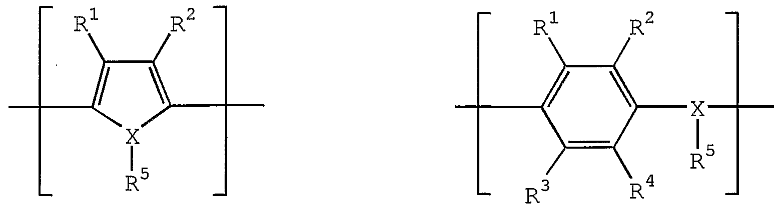
- the organic semiconductor is at least one member selected from an organic semiconductor comprising benzopyrroline tetramer and chloranil, an organic semiconductor mainly comprising tetrathiotetracene, an organic semiconductor mainly comprising tetra- cyanoquinodimethane, and an organic semiconductor mainly comprising an electrically conducting polymer obtained by doping a dopant to a polymer containing a repeating unit represented by the following formula (1) or (2) :
- R 1 to R 4 which may be the same or different, each represents a hydrogen atom, an alkyl group having from 1 to 6 carbon atoms or an alkoxy group having from 1 to 6 carbon atoms
- X represents an oxygen atom, a sulfur atom or a nitrogen atom
- R 5 is present only when X is a nitrogen atom
- each of the pairs R 1 and R 2 , and R 3 and R 4 may combine with each other to form a ring structure.
- (1) is an electrically conducting polymer containing a structure unit represented by the following formula (3) as a repeating unit:
- each of R 6 and R 7 independently represents a hydrogen atom, a linear or branched, saturated or unsaturated alkyl group having from 1 to 6 carbon atoms, or a substituent for forming at least one 5-, 6- or 7-membered saturated hydrocarbon ring structure containing two oxygen atoms when the alkyl groups are combined with each other at an arbitrary position, and the ring structure includes a structure having a vinylene bond which may be substituted, and a phenylene structure which may be substituted.
- a method for producing a solid electrolytic capacitor element comprising a step of electrochemically forming the sintered body electrode described in any one of 1 to 7 above to form a dielectric layer on the surface thereof, and a step of forming the other electrode on the dielectric layer. 19.
- Fig. 1 is a perspective view showing one example of the chip solid electrolytic capacitor of the present invention.
- the sintered body electrode of the present invention comprises at least one member selected from an earth-acid metal, an alloy mainly comprising an earth-acid metal, an oxide of an earth-acid metal, and a mixture of two or more thereof.
- "mainly comprising” means to comprise the component in an amount of 50 mass% or more.
- the sintered body electrode can be usually produced by appropriately shaping a powder (raw material powder) of the above-described metal, alloy, oxide or mixture together with a binder and after removing the binder, sintering the shaped article.
- the production method of the sintered body electrode is not particularly limited, and one example thereof is described below.
- a starting material powder is press-formed into a predetermined shape to obtain a shaped article.
- This shaped article is heated at 500 to 2,000°C under 10 "4 to 10 "1 Pa for several minutes to several hours to obtain a sintered body.
- a part of a metal wire mainly comprising a valve-acting metal such as tantalum, niobium and aluminum may be embedded in the shaped article at the shaping and sintered simultaneously with the shaped article, so that the metal wire in the portion protruded from the sintered body can be used as the anode outgoing wire of the sintered body electrode.
- the metal wire may be connected by welding or the like after sintering and used as the anode outgoing wire.
- the diameter of such a metal wire is usually 1 mm or less.
- the above-described powder may be attached to a valve-acting metal foil such as tantalum and niobium and sintered to produce a sintered body electrode where a part of the valve-acting metal foil is working as the anode part.
- a valve-acting metal foil such as tantalum and niobium
- the earth-acid metal means an element belonging to Group 5 of the Periodic Table, specifically, vanadium, tantalum or niobium.
- the earth- acid metal is preferably tantalum or niobium.
- the alloy mainly comprising an earth-acid metal includes those mainly comprising tantalum and/or niobium and containing, as an alloy component, at least one element selected from the group consisting of elements belonging to Groups 2 to 16 of the Periodic Table.
- the electrically conducting oxide of an earth-acid metal includes tantalum oxide and niobium oxide.
- a representative electrically conducting oxide of an earth-acid metal is niobium monoxide. These may be used individually or as a mixture of two or more thereof.
- a part of the earth-acid metal, alloy or electrically conducting oxide of an earth-acid metal may be subjected to at least one treatment selected from carbidation, phosphation, boronation, nitridation and sulfidation before use .
- the pseudo-closed porosity defined below is 11% or less, preferably 7% or less.
- the capacitor element produced by using a semiconductor layer for the counter electrode can have a higher capacitance appearance factor.
- the pseudo-closed porosity means a value obtained by dividing the difference between the volume of a sintered body measured under atmospheric pressure and the volume measured in a vacuum, which are determined according to the Archimedes method (a method to determine the density of a sample using the principle that the buoyancy which a solid in liquid receives is equal to the mass of liquid having the same volume of the solid (Archimedes' principle)), by the volume measured under atmospheric pressure.
- the weight of a sintered body for electrode after cutting out the lead wire (described later) from the basal end is measured in air and in pure water, the volume of pure water displaced by the sintered body is determined from the difference of the weights measured
- Pseudo-closed porosity (%) ⁇ (volume under atmospheric pressure - volume in a vacuum) / (volume under atmospheric pressure) ⁇ x 100
- the pseudo-closed porosity usually tends to increase when the amount of binder is increased, when the CV value of the starting material powder used is high, when the sintering temperature is elevated, or when the density of the sintered body is high.
- the pseudo-closed porosity decreases when etching is applied.
- binder examples include acrylic resin, polyvinyl alcohol, camphor and iodide.
- the amount of the binder used is usually from 0.1 to 20 parts by mass per 100 parts by mass of the earth-acid metal, alloy and/or electrically conducting oxide.
- the sintered body electrode of the present invention preferably has an entire porosity of 40 to 70 vol%.
- a sintered body having a specific surface area of 1 to 16 m 2 /g before etching is preferably used.
- the specific surface area may increase by about 10% after etching but is usually almost the same before and after etching.
- the sintered body of the present invention When the sintered body of the present invention is electrochemically formed at 80°C and a predetermined voltage for 300 minutes in an aqueous 0.1% phosphoric acid solution, it exhibits a CV value of 50,000 to 340,000 ⁇ F'V/g (a value measured at 120 Hz with a bias of 1.5 V for 30 seconds at room temperature in an aqueous 30% sulfuric acid solution) . If the CV value is less than 50,000 ⁇ F-V/g, a capacitor having a large capacitance cannot be obtained, whereas if it exceeds 340,000 ⁇ F'V/g, the capacitor has a lower capacitance appearance factor even when the pseudo- closed porosity is adjusted.
- the capacitance appearance factor decreases when the volume of the sintered body electrode exceeds 4 mm 3 .
- the capacitor produced using it can advantageously exhibit a good capacitance appearance factor.
- the sintered body electrode of the present invention is not particularly limited in the size and may have, for example, a volume of 4 to 550 mm 2 .
- the volume of the sintered body electrode can be made large and therefore, the capacitor produced using the electrode can be made to have an ultrahigh capacitance comparable with an electric double layer capacitor.
- a solid electrolytic capacitor can be produced from one electrode which is the sintered body electrode of the present invention, the other electrode and a dielectric oxide film layer interposed therebetween.
- the dielectric oxide film layer of the solid electrolytic capacitor examples include a dielectric oxide film layer mainly comprising diniobium pentoxide or ditantalum pentoxide.
- the dielectric oxide film layer mainly comprising diniobium pentoxide can be obtained by electrochemically forming the niobium sintered body electrode used for one electrode in an electrolytic solution.
- the niobium sintered body electrode is electrochemically formed in an electrolytic solution usually by using an aqueous protonic acid solution, for example, an aqueous 0.1% acetic acid solution or an aqueous 0.1% phosphoric acid solution.
- the semiconductor layer formed on the dielectric oxide film layer of the present invention include at least one compound selected from an organic semiconductor and an inorganic semiconductor.
- the organic semiconductor include an organic semiconductor comprising benzopyrroline tetramer and chloranil, an organic semiconductor mainly comprising tetrathiotetracene, an organic semiconductor mainly comprising tetracyanoquinodimethane, and an organic semiconductor mainly comprising an electrically conducting polymer obtained by doping a dopant to a polymer containing a repeating unit represented by the following formula (1) or (2)
- R 1 to R 4 which may be the same or different, each represents a hydrogen atom, an alkyl group having from 1 to 6 carbon atoms or an alkoxy group having from 1 to 6 carbon atoms
- X represents an oxygen atom, a sulfur atom or a nitrogen atom
- R 5 is present only when X is a nitrogen atom
- each of the pairs R 1 and R 2 , and R 3 and R 4 may combine with each other to form a ring structure.
- (1) is preferably an electrically conducting polymer containing a structure unit represented by the following formula (3) as a repeating unit:
- each of R 6 and R 7 independently represents a hydrogen atom, a linear or branched, saturated or unsaturated alkyl group having from 1 to 6 carbon atoms, or a substituent for forming at least one 5-, 6- or 7-membered saturated hydrocarbon ring structure containing two oxygen atoms when the alkyl groups are combined with each other at an arbitrary position, and the ring structure includes a structure having a vinylene bond which may be substituted, and a phenylene structure which may be substituted.
- the electrically, conducting polymer containing such a chemical structure is being electrically charged and a dopant is doped therein.
- a dopant known dopants can be used without limitation.
- the polymer containing a repeating unit represented by formula (1) , (2) or (3) include polyaniline, polyoxyphenylene, polyphenylene sulfide, polythiophene, polyfuran, polypyrrole, polymethylpyrrole, and substitution derivatives and copolymers thereof.
- the inorganic semiconductor include at least one compound selected from molybdenum dioxide, tungsten dioxide, lead dioxide and manganese dioxide.
- an electrically conducting layer is provided on the semiconductor layer formed by the above-described method or the like.
- the electrically conducting layer can be formed, for example, by the solidification of an electrically conducting paste, plating, vapor deposition of metal, or adhesion of a heat-resistant electrically conducting resin film.
- Preferred examples of the electrically conducting paste include silver paste, copper paste, aluminum paste, carbon paste and nickel paste, and these may be used individually or in combination of two or more thereof. In the case of using two or more pastes, the pastes may be mixed or may be superposed one on another as separate layers. The electrically conducting paste applied is then solidified by allowing it to stand in air or under heating.
- Examples of the plating include nickel plating, copper plating, silver plating and aluminum plating.
- Examples of the metal vapor-deposited include aluminum, nickel, copper and silver.
- carbon paste and silver paste are stacked in this order on the sintered body having formed thereon the semiconductor layer.
- a solid electrolytic capacitor element where layers up to the electrically conducting layer are stacked on the sintered body to form the cathode part is produced.
- One or a plurality of the solid electrolytic capacitor element (s) having such a constitution of the present invention is (are) jacketed, for example, by resin mold, resin case, metallic jacket case, resin dipping or laminate film and thereby, can be completed as a capacitor product for various uses.
- the jacketing with resin mold is described. As shown in Fig.
- a part of the cathode part (3) of the solid electrolytic capacitor element (2) is placed on one end part (a) of a separately prepared lead frame (1) having a pair of oppositely disposed end parts (la and lb) , the anode outgoing part (anode part) (4) or anode lead (4a) of the sintered body is placed on the other end part (lb) of the lead frame, each is electrically or mechanically joined, for example, by solidification of an electrically conducting paste for the former and by spot-welding for the latter, the entirety is molded with a resin to form a jacket part (chip molding resin) (5) while leaving outside a part of the end part of the lead frame, and the lead frame is cut and bent at predetermined portions outside the resin mold, thereby producing the solid electrolytic capacitor of the present invention.
- the lead frame is cut as described above and ultimately works out to external terminals of the solid electrolytic capacitor.
- the shape thereof is a foil or plate form and for the construction material of the lead frame, iron, copper, aluminum or an alloy mainly comprising such a metal is predominantly used.
- the lead frame may be partially or entirely plated with solder, tin, titanium or the like. Between the lead frame and the plating, a primer plating such as nickel may be provided.
- a pair of oppositely disposed end parts are present and a gap is provided between these end parts, whereby the anode part and the cathode part of each solid electrolytic capacitor element can be insulated from each other.
- the resin used in molding the solid electrolytic capacitor of the present invention known resins for use in molding a solid electrolytic capacitor, such as epoxy resin, phenol resin and alkyd resin, can be used.
- the production machine used for performing the molding with resin is preferably a transfer machine.
- the solid electrolytic capacitor of the present invention can be preferably used for circuits using a high- capacitance capacitor, such as voltage stabilizing circuit and noise removing circuit. These circuits can be used in various digital devices such as a personal computer, server, camera, game machine, DVD, AV device and cellular phone, and electronic devices such as various power sources.
- the solid electrolytic capacitor produced in the present invention has large capacitance for the constant volume and therefore, by using this solid electrolytic capacitor, electronic circuits and electronic devices having a small size and less fluctuation of voltage can be obtained.
- the protruding lead wire of the sintered body electrode was cut out from the basal end and the sintered body was suspended in air or in pure water and measured on the weight in each state. From the difference of the weights measured (buoyancy) and the density of pure water, the volume of pure water displaced by the sintered body was determined.
- the volume of a sintered body electrode after cutting out the protruded lead wire from the basal end was determined from the outside dimension thereof, the bulk density was calculated from the obtained volume and the mass of the sintered body electrode, and the entire porosity was calculated according to the following formula.
- the true density employed was 16.69 g/cm 3 for tantalum and 8.57 g/cm 3 for niobium (see, The Merck Index, 11th ed.). Equation 3
- a tantalum powder having a CV value of 150,000 ⁇ F'V/g was left standing in a nitrogen atmosphere to provide a partially nitrided tantalum powder having a nitrided amount of 12,000 ppm by mass.
- This tantalum powder (38+3 mg) and an acryl binder (polyhexyl methacrylate, produced by Aldrich) in an amount shown in Table 1 were dissolved in toluene and by using the obtained 10 mass% solution and a tantalum lead wire (0.24 mm ⁇ ) , a shaped article having a size of 4.0x1.0x1.8 mm was produced.
- a part of the lead wire was embedded in parallel to the longitudinal direction of the shaped article and the remaining was protruded from the shaped article.
- the protruded lead wire part works out to the anode part of an element.
- the shaped article produced was sintered at 10 ⁇ 3 to 10 "4 Pa under the conditions shown in Table 1 to obtain a sintered body.
- the bulk density of each sintered body obtained is also shown in Table 1.
- Each sintered body was left standing in 10 mass% hydrofluoric acid for 15 minutes and then the sintered body excluding a part of the anode outgoing wire was dipped in an aqueous 5 mass% tetramethylammonium hydroxide solution and etched at a current density of 0.5 mA/unit by using a carbon electrode for the counter electrode.
- the CV, specific surface area, pseudo-closed porosity and entire porosity of each sintered body obtained were measured. The results are shown in Table 2.
- Each sintered body excluding a part of the lead wire was dipped in an aqueous 0.1% phosphoric acid solution and electrochemically formed at 80°C for 10 hours by applying 9 V between the sintered body and a tantalum plate electrode as the cathode to form a dielectric oxide film layer composed of Ta 2 0 5 .
- a lead frame comprising a 100 ⁇ m-thick copper alloy having a tin-plated surface was separately prepared, where a pair of end parts each in a width of 3.4 mm were present, the end part on which the cathode part was laid had a step of 0.5 mm, and the portion where the cathode part was laid had a length of 4.3 mm (see Fig. 1) .
- the cathode side of the solid electrolytic capacitor element was laid on the end part having a step and connected by the solidification of silver paste and the lead wire as the element anode was electrically and mechanically connected to the other end part by spot welding.
- both end parts of the lead frame and the solid electrolytic capacitor element were molded with epoxy resin by transfer molding to produce a chip solid electrolytic capacitor in a size of 7.3x4.3x1.8 mm.
- both protruded parts outside the mold each was cut at the position of 2.9 mm from the end face of the mold, the frames cut out were removed, and the end parts connected to the chip solid electrolytic capacitor and remaining outside each was bent along the outer circumference of the capacitor and used as the external terminal .
- the capacitor using the sintered body has a large capacitance appearance factor.
- the pseudo-closed porosity of the sintered body can be adjusted by appropriately selecting the amount of binder, the sintering temperature and the density of sintered body.
- Niobium powders having various CV values shown in Table 3 each was left standing in a nitrogen atmosphere to provide a partially nitrided niobium powder having a nitrided amount of 12,000 ppm by mass.
- This niobium powder (81+4 mg) and an acryl binder (polyhexyl methacrylate, produced by Aldrich) in an amount shown in Table 3 were dissolved in toluene and by using the obtained 10 mass% solution and a niobium lead wire (0.29 mm ⁇ ) , a shaped article having a size of 4.0x3.2x1.7 mm was produced.
- a part of the lead wire was embedded in parallel to the longitudinal direction of the shaped article and the remaining was protruded from the shaped article.
- the protruded lead wire part works out to the element anode part.
- the shaped article produced was sintered at 10 "3 to 10 "4 Pa under the conditions shown in Table 3 to obtain a sintered body.
- the bulk density of each sintered body obtained is shown together in Table 3.
- Each sintered body was left standing in 10 mass% hydrofluoric acid for 15 minutes and then the sintered body excluding a part of the anode outgoing wire was dipped in an aqueous 5 mass% potassium hydroxide solution and etched at a current density of 0.5 mA/unit by using a carbon electrode for the counter electrode.
- the CV, specific surface area, pseudo-closed porosity and entire porosity of each sintered body obtained were measured. The results are shown in Table 4.
- Each sintered body excluding a part of the lead wire was dipped in an aqueous 0.1% phosphoric acid solution and electrochemically formed at 80°C for 10 hours by applying 20 V between the sintered body and a tantalum plate electrode as the cathode to form a dielectric oxide film layer comprising Nb 2 0 5 .
- a semiconductor layer comprising polyethylenedioxythiophene was formed (by dipping the sintered body in an aqueous solution containing ethylene- dioxythiophene and anthraquinonesulfonic acid, each dissolved in a trace amount, and performing electrolytic polymerization for 210 hours) .
- carbon paste and silver paste were sequentially stacked to complete the cathode part, thereby producing a solid electrolytic capacitor element.
- a lead frame comprising a 100 ⁇ m-thick copper alloy having a tin-plated surface was separately prepared, where a pair of end parts each in a width of 3.4 mm were present, the end part on which the cathode part was laid had a step of 0.9 mm, and the portion where the cathode part was laid had a length of 4.3 mm (see Fig. 1) .
- the cathode side of the solid electrolytic capacitor element was laid on the end part having a step and connected by the solidification of silver paste and the lead wire as the element anode was electrically and mechanically connected to the other end part by spot welding.
- a solid electrolytic capacitor was produced in the same manner as in Example 10 except that the sintered body was not subjected to a treatment with hydrofluoric acid and a treatment of electrical etching.
- the pseudo-closed porosity and entire porosity of the sintered body produced and the capacitance appearance factor of the solid electrolytic capacitor are shown in Table 5 together with the values of Example 10.
- the pseudo-closed porosity changes according to the presence or absence of etching and when the pseudo-closed porosity exceeds 11%, the capacitance appearance factor decreases .
- a solid electrolytic capacitor was produced in the same manner as in Comparative Example 7 except that the size of the shaped article was changed from 4.0x3.2x1.7 mm
- a niobium powder having a CV value of 130,000 ⁇ F'V/g was left standing in a nitrogen atmosphere to provide a partially nitrided niobium powder having a nitrided amount of 14,000 ppm by mass.
- This niobium powder (654+12 mg) and 50 mg of an acryl binder (polyhexyl methacrylate, produced by Aldrich) were dissolved in toluene and by using the obtained 10 mass% solution and a niobium lead wire (0.33 mm ⁇ ), a shaped article having a size of 9.6x2.1x9.6 mm was produced.
- a part of the lead wire was embedded in the direction perpendicular to the 9.6x2.1 mm face of the shaped article and the remaining was protruded from the shaped article.
- the protruded lead wire part works out to the element anode part.
- the shaped article produced was sintered under the same conditions as in Example 7 (1,280°C, 30 minutes, 10 "3 to 10 "4 Pa) to obtain a sintered body.
- This sintered body was left standing in 10 mass% hydrofluoric acid for 15 minutes and then the sintered body excluding a part of the anode outgoing wire was dipped in an aqueous 5 mass% tetramethylammonium hydroxide solution and etched at a current density of 0.5 mA/unit by using a carbon electrode for the counter electrode.
- the pseudo- closed porosity of the sintered body produced was 8% and the entire porosity was 55.5%.
- This sintered body excluding a part of the lead wire was dipped in an aqueous 0.1% phosphoric acid solution and electrochemically formed at 80°C for 10 hours by applying 20 V between the sintered body and a tantalum plate electrode as the cathode to form a dielectric oxide film layer composed of Nb 2 0 5 .
- a sintered body and then a solid electrolytic capacitor were produced in the same manner as in Example 13 except that the sintering conditions were changed from the same conditions as in Example 7 (1,280°C, 30 minutes, 10 "3 to 10 ⁇ 4 Pa) to the same conditions as in Comparative Example 4 (1,310°C, 30 minutes, 10 "3 to 10 "4 Pa) and the etching treatment was not performed.
- the pseudo-closed porosity and entire porosity of the sintered body produced and the capacitance appearance factor of the solid electrolytic capacitor were 17%, 54.7% and 72%, respectively.
- the results in Example 13 and Comparative Example 8 are shown in Table 7. As seen from the results in Table 7, the pseudo-closed porosity varies depending on the presence or absence of etching and the sintering temperature and when the pseudo-closed porosity exceeds 11%, the capacitance appearance factor decreases. Table 7
- a solid electrolytic capacitor having an excellent capacitance appearance factor can be produced.
- a solid electrolytic capacitor having an excellent capacitance appearance factor can be produced by adjusting the pseudo-closed porosity to 11% or less .
- the pseudo-closed porosity of the sintered body can be easily adjusted to 11% or less without particularly providing a new step by appropriately selecting the amount of binder, the sintering conditions, the density of sintered body, and the like at the time of producing the shaped article, or by selecting the etching conditions.
Abstract
Description


Claims

Priority Applications (6)
| Application Number | Priority Date | Filing Date | Title |
|---|---|---|---|
| AT04727099T ATE482458T1 (en) | 2003-04-14 | 2004-04-13 | SINTERED BODY ELECTRODE AND SOLID ELECTROLYTIC CAPACITOR WITH THE ELECTRODE |
| EP04727099A EP1618574B1 (en) | 2003-04-14 | 2004-04-13 | Sintered body electrode and solid electrolytic capacitor using the electrode |
| DE602004029243T DE602004029243D1 (en) | 2003-04-14 | 2004-04-13 | SINTER BODY ELECTRODE AND FIXED ELECTROLYTIC CAPACITOR WITH THE ELECTRODE |
| KR1020057019691A KR101100100B1 (en) | 2003-04-14 | 2004-04-13 | Sintered body electrode and solid electrolytic capacitor using the electrode |
| US10/552,589 US7423863B2 (en) | 2003-04-14 | 2004-04-13 | Sintered body electrode and solid electrolytic capacitor using the electrode |
| CN2004800101416A CN1774778B (en) | 2003-04-14 | 2004-04-13 | Sintered body electrode and solid electrolytic capacitor using the electrode |
Applications Claiming Priority (4)
| Application Number | Priority Date | Filing Date | Title |
|---|---|---|---|
| JP2003-109146 | 2003-04-14 | ||
| JP2003109146 | 2003-04-14 | ||
| US46410703P | 2003-04-21 | 2003-04-21 | |
| US60/464,107 | 2003-04-21 |
Publications (2)
| Publication Number | Publication Date |
|---|---|
| WO2004093106A2 true WO2004093106A2 (en) | 2004-10-28 |
| WO2004093106A3 WO2004093106A3 (en) | 2005-04-14 |
Family
ID=35501524
Family Applications (1)
| Application Number | Title | Priority Date | Filing Date |
|---|---|---|---|
| PCT/JP2004/005235 WO2004093106A2 (en) | 2003-04-14 | 2004-04-13 | Sintered body electrode and solid electrolytic capacitor using the electrode |
Country Status (9)
| Country | Link |
|---|---|
| US (1) | US7423863B2 (en) |
| EP (1) | EP1618574B1 (en) |
| JP (1) | JP4566593B2 (en) |
| KR (1) | KR101100100B1 (en) |
| CN (1) | CN1774778B (en) |
| AT (1) | ATE482458T1 (en) |
| DE (1) | DE602004029243D1 (en) |
| TW (1) | TW200506985A (en) |
| WO (1) | WO2004093106A2 (en) |
Cited By (1)
| Publication number | Priority date | Publication date | Assignee | Title |
|---|---|---|---|---|
| US10079111B2 (en) | 2013-01-18 | 2018-09-18 | Toyo Aluminium Kabushiki Kaisha | Method for producing electrode material for aluminum electrolytic capacitors, and electrode material for aluminum electrolytic capacitors |
Families Citing this family (13)
| Publication number | Priority date | Publication date | Assignee | Title |
|---|---|---|---|---|
| TWI469163B (en) * | 2004-12-24 | 2015-01-11 | Showa Denko Kk | Solid electrolytic capacitor element, solid electrolytic capacitor and manufacturing method thereof |
| WO2006106703A1 (en) * | 2005-03-30 | 2006-10-12 | Showa Denko K. K. | Solid electrolytic capacitor element, method for manufacturing same, and solid electrolytic capacitor |
| DE102005043828A1 (en) * | 2005-09-13 | 2007-03-22 | H.C. Starck Gmbh | Process for the preparation of electrolytic capacitors |
| US7352563B2 (en) * | 2006-03-13 | 2008-04-01 | Avx Corporation | Capacitor assembly |
| US7724502B2 (en) * | 2007-09-04 | 2010-05-25 | Avx Corporation | Laser-welded solid electrolytic capacitor |
| US7768773B2 (en) * | 2008-01-22 | 2010-08-03 | Avx Corporation | Sintered anode pellet etched with an organic acid for use in an electrolytic capacitor |
| CN102017034B (en) * | 2008-04-22 | 2016-01-27 | 东洋铝株式会社 | For the electrode material of aluminium electrolytic capacitor and the method for this electrode material of manufacture |
| US8974957B2 (en) * | 2008-10-22 | 2015-03-10 | Lg Chem, Ltd. | Cathode active material providing improved efficiency and energy density of electrode |
| JPWO2012161158A1 (en) | 2011-05-26 | 2014-07-31 | 東洋アルミニウム株式会社 | Electrode material for aluminum electrolytic capacitor and method for producing the same |
| JP5769528B2 (en) | 2011-07-15 | 2015-08-26 | 東洋アルミニウム株式会社 | Electrode material for aluminum electrolytic capacitor and method for producing the same |
| KR102079032B1 (en) | 2012-02-10 | 2020-02-19 | 도요 알루미늄 가부시키가이샤 | Method for manufacturing electrode material for aluminium electrolytic capacitor |
| US20170040108A1 (en) * | 2015-08-06 | 2017-02-09 | Murata Manufacturing Co., Ltd. | Capacitor |
| CN112053849B (en) * | 2020-07-23 | 2021-06-15 | 新疆众和股份有限公司 | Preparation method of electrode foil |
Citations (6)
| Publication number | Priority date | Publication date | Assignee | Title |
|---|---|---|---|---|
| JPH02254108A (en) * | 1989-03-29 | 1990-10-12 | Permelec Electrode Ltd | Tantalum sintered body and its production |
| EP0626358A2 (en) * | 1993-05-27 | 1994-11-30 | Kai Yin Dr. Chia | Electrically conductive high strength dense ceramic |
| EP1137021A1 (en) * | 1998-08-05 | 2001-09-26 | Showa Denko Kabushiki Kaisha | Sinter of niobium for capacitor, and method of manufacture thereof |
| JP2001330544A (en) * | 2000-05-22 | 2001-11-30 | Nikko Materials Co Ltd | Method for measuring density of sintered body |
| WO2002092864A2 (en) * | 2001-05-15 | 2002-11-21 | Showa Denko K. K. | Niobium powder, niobium sintered body and capacitor using the sintered body |
| JP2003166002A (en) * | 2001-11-30 | 2003-06-13 | Cabot Supermetal Kk | Niobium powder or tantalum powder, manufacturing method therefor, porous compact using it, and solid electrolytic capacitor |
Family Cites Families (15)
| Publication number | Priority date | Publication date | Assignee | Title |
|---|---|---|---|---|
| US4097911A (en) * | 1975-10-06 | 1978-06-27 | Erie Technological Products, Inc. | Base metal electrode capacitor and method of making the same |
| US4101952A (en) * | 1976-08-17 | 1978-07-18 | Sprague Electric Company | Monolithic base-metal glass-ceramic capacitor |
| JPS55128816A (en) | 1979-03-27 | 1980-10-06 | Marukon Denshi Kk | Tantalum solid electrolytic condenser |
| US5034857A (en) * | 1989-10-06 | 1991-07-23 | Composite Materials Technology, Inc. | Porous electrolytic anode |
| JP2770636B2 (en) * | 1992-03-03 | 1998-07-02 | 日本電気株式会社 | Chip type solid electrolytic capacitor |
| JP3229121B2 (en) * | 1994-05-27 | 2001-11-12 | ローム株式会社 | Structure of solid electrolytic capacitor |
| JPH10149955A (en) * | 1996-11-18 | 1998-06-02 | Rohm Co Ltd | Manufacture of porous chip body for capacitor element of solid-state electrolytic capacitor |
| JP3343496B2 (en) * | 1997-04-28 | 2002-11-11 | マルコン電子株式会社 | Solid capacitor and manufacturing method thereof |
| JPH11283874A (en) * | 1998-01-28 | 1999-10-15 | Matsushita Electric Ind Co Ltd | Electrolytic capacitor |
| MXPA01002547A (en) * | 1998-09-10 | 2004-06-03 | Starck H C Gmbh | Paste for producing sintered refractory metal layers, notably earth acid metal electrolytic capacitors or anodes. |
| DE19847012A1 (en) * | 1998-10-13 | 2000-04-20 | Starck H C Gmbh Co Kg | Niobium powder and process for its manufacture |
| JP2001172701A (en) * | 1999-12-14 | 2001-06-26 | Showa Kyabotto Super Metal Kk | Niobium powder, producing method therefor, porous sintered body using same niobium powder and solid electrolytic capacitor |
| JP4160223B2 (en) * | 1999-12-14 | 2008-10-01 | ローム株式会社 | Solid electrolytic capacitor |
| JP4647744B2 (en) * | 2000-04-21 | 2011-03-09 | 昭和電工株式会社 | Niobium powder for capacitor, sintered body using the same, and capacitor using the same |
| CN100351963C (en) * | 2001-11-08 | 2007-11-28 | 松下电器产业株式会社 | Capacitor and production method therefor |
-
2004
- 2004-03-25 JP JP2004088547A patent/JP4566593B2/en not_active Expired - Lifetime
- 2004-04-13 CN CN2004800101416A patent/CN1774778B/en not_active Expired - Lifetime
- 2004-04-13 AT AT04727099T patent/ATE482458T1/en not_active IP Right Cessation
- 2004-04-13 KR KR1020057019691A patent/KR101100100B1/en active IP Right Grant
- 2004-04-13 EP EP04727099A patent/EP1618574B1/en not_active Expired - Lifetime
- 2004-04-13 DE DE602004029243T patent/DE602004029243D1/en not_active Expired - Lifetime
- 2004-04-13 US US10/552,589 patent/US7423863B2/en active Active
- 2004-04-13 WO PCT/JP2004/005235 patent/WO2004093106A2/en active Application Filing
- 2004-04-14 TW TW093110378A patent/TW200506985A/en unknown
Patent Citations (6)
| Publication number | Priority date | Publication date | Assignee | Title |
|---|---|---|---|---|
| JPH02254108A (en) * | 1989-03-29 | 1990-10-12 | Permelec Electrode Ltd | Tantalum sintered body and its production |
| EP0626358A2 (en) * | 1993-05-27 | 1994-11-30 | Kai Yin Dr. Chia | Electrically conductive high strength dense ceramic |
| EP1137021A1 (en) * | 1998-08-05 | 2001-09-26 | Showa Denko Kabushiki Kaisha | Sinter of niobium for capacitor, and method of manufacture thereof |
| JP2001330544A (en) * | 2000-05-22 | 2001-11-30 | Nikko Materials Co Ltd | Method for measuring density of sintered body |
| WO2002092864A2 (en) * | 2001-05-15 | 2002-11-21 | Showa Denko K. K. | Niobium powder, niobium sintered body and capacitor using the sintered body |
| JP2003166002A (en) * | 2001-11-30 | 2003-06-13 | Cabot Supermetal Kk | Niobium powder or tantalum powder, manufacturing method therefor, porous compact using it, and solid electrolytic capacitor |
Non-Patent Citations (3)
| Title |
|---|
| PATENT ABSTRACTS OF JAPAN vol. 015, no. 002 (M-1065), 7 January 1991 (1991-01-07) & JP 02 254108 A (PERMELEC ELECTRODE LTD), 12 October 1990 (1990-10-12) * |
| PATENT ABSTRACTS OF JAPAN vol. 2002, no. 03, 3 April 2002 (2002-04-03) & JP 2001 330544 A (NIKKO MATERIALS CO LTD), 30 November 2001 (2001-11-30) * |
| PATENT ABSTRACTS OF JAPAN vol. 2003, no. 10, 8 October 2003 (2003-10-08) & JP 2003 166002 A (CABOT SUPERMETAL KK), 13 June 2003 (2003-06-13) * |
Cited By (1)
| Publication number | Priority date | Publication date | Assignee | Title |
|---|---|---|---|---|
| US10079111B2 (en) | 2013-01-18 | 2018-09-18 | Toyo Aluminium Kabushiki Kaisha | Method for producing electrode material for aluminum electrolytic capacitors, and electrode material for aluminum electrolytic capacitors |
Also Published As
| Publication number | Publication date |
|---|---|
| EP1618574B1 (en) | 2010-09-22 |
| CN1774778A (en) | 2006-05-17 |
| KR101100100B1 (en) | 2011-12-29 |
| TWI331350B (en) | 2010-10-01 |
| KR20060005370A (en) | 2006-01-17 |
| DE602004029243D1 (en) | 2010-11-04 |
| US20060204735A1 (en) | 2006-09-14 |
| WO2004093106A3 (en) | 2005-04-14 |
| TW200506985A (en) | 2005-02-16 |
| EP1618574A2 (en) | 2006-01-25 |
| ATE482458T1 (en) | 2010-10-15 |
| US7423863B2 (en) | 2008-09-09 |
| JP4566593B2 (en) | 2010-10-20 |
| CN1774778B (en) | 2010-06-16 |
| JP2004336018A (en) | 2004-11-25 |
Similar Documents
| Publication | Publication Date | Title |
|---|---|---|
| KR101554049B1 (en) | Solid Electrolytic Capacitor and Method of Manufacturing thereof | |
| JP4596543B2 (en) | Manufacturing method of solid electrolytic capacitor | |
| US7423863B2 (en) | Sintered body electrode and solid electrolytic capacitor using the electrode | |
| US7522404B2 (en) | Solid electrolytic capacitor and the use thereof | |
| WO2001082318A2 (en) | Niobium sintered body, production method therefor, and capacitor using the same | |
| JP4809463B2 (en) | Method for manufacturing sintered tantalum and method for manufacturing capacitor | |
| JPWO2003008673A1 (en) | Metal foil made of an earth metal alloy and a capacitor having the same | |
| US7218505B2 (en) | Chip solid electrolyte capacitor | |
| US6855184B2 (en) | Niobium powder, sintered body thereof and capacitor using the same | |
| EP1435102A2 (en) | Tantalum capacitor with niobium alloy lead wire | |
| US7355842B2 (en) | Chip solid electrolyte capacitor and production method of the same | |
| EP1264321A4 (en) | Niobium powder for capacitor, sintered body thereof and capacitor using the sintered body | |
| JP4260443B2 (en) | Capacitor powder, sintered body using the same, and capacitor using the same |
Legal Events
| Date | Code | Title | Description |
|---|---|---|---|
| AK | Designated states |
Kind code of ref document: A2 Designated state(s): AE AG AL AM AT AU AZ BA BB BG BR BW BY BZ CA CH CN CO CR CU CZ DE DK DM DZ EC EE EG ES FI GB GD GE GH GM HR HU ID IL IN IS KE KG KP KR KZ LC LK LR LS LT LU LV MA MD MG MK MN MW MX MZ NA NI NO NZ OM PG PH PL PT RO RU SC SD SE SG SK SL SY TJ TM TN TR TT TZ UA UG US UZ VC VN YU ZA ZM ZW |
|
| AL | Designated countries for regional patents |
Kind code of ref document: A2 Designated state(s): BW GH GM KE LS MW MZ SD SL SZ TZ UG ZM ZW AM AZ BY KG KZ MD RU TJ TM AT BE BG CH CY CZ DE DK EE ES FI FR GB GR HU IE IT LU MC NL PL PT RO SE SI SK TR BF BJ CF CG CI CM GA GN GQ GW ML MR NE SN TD TG |
|
| 121 | Ep: the epo has been informed by wipo that ep was designated in this application | ||
| WWE | Wipo information: entry into national phase |
Ref document number: 10552589 Country of ref document: US |
|
| WWE | Wipo information: entry into national phase |
Ref document number: 20048101416 Country of ref document: CN Ref document number: 1020057019691 Country of ref document: KR |
|
| WWE | Wipo information: entry into national phase |
Ref document number: 2004727099 Country of ref document: EP |
|
| WWP | Wipo information: published in national office |
Ref document number: 1020057019691 Country of ref document: KR |
|
| WWP | Wipo information: published in national office |
Ref document number: 2004727099 Country of ref document: EP |
|
| WWP | Wipo information: published in national office |
Ref document number: 10552589 Country of ref document: US |