WO2004016822A2 - Method for obtaining a thin, stabilized fluorine-doped silica layer, resulting thin layer and use thereof in ophthalmic optics - Google Patents
Method for obtaining a thin, stabilized fluorine-doped silica layer, resulting thin layer and use thereof in ophthalmic optics Download PDFInfo
- Publication number
- WO2004016822A2 WO2004016822A2 PCT/FR2003/002487 FR0302487W WO2004016822A2 WO 2004016822 A2 WO2004016822 A2 WO 2004016822A2 FR 0302487 W FR0302487 W FR 0302487W WO 2004016822 A2 WO2004016822 A2 WO 2004016822A2
- Authority
- WO
- WIPO (PCT)
- Prior art keywords
- layer
- sio
- silicon
- layers
- thin
- Prior art date
Links
Classifications
-
- G—PHYSICS
- G02—OPTICS
- G02B—OPTICAL ELEMENTS, SYSTEMS OR APPARATUS
- G02B1/00—Optical elements characterised by the material of which they are made; Optical coatings for optical elements
- G02B1/10—Optical coatings produced by application to, or surface treatment of, optical elements
- G02B1/11—Anti-reflection coatings
- G02B1/111—Anti-reflection coatings using layers comprising organic materials
-
- C—CHEMISTRY; METALLURGY
- C23—COATING METALLIC MATERIAL; COATING MATERIAL WITH METALLIC MATERIAL; CHEMICAL SURFACE TREATMENT; DIFFUSION TREATMENT OF METALLIC MATERIAL; COATING BY VACUUM EVAPORATION, BY SPUTTERING, BY ION IMPLANTATION OR BY CHEMICAL VAPOUR DEPOSITION, IN GENERAL; INHIBITING CORROSION OF METALLIC MATERIAL OR INCRUSTATION IN GENERAL
- C23C—COATING METALLIC MATERIAL; COATING MATERIAL WITH METALLIC MATERIAL; SURFACE TREATMENT OF METALLIC MATERIAL BY DIFFUSION INTO THE SURFACE, BY CHEMICAL CONVERSION OR SUBSTITUTION; COATING BY VACUUM EVAPORATION, BY SPUTTERING, BY ION IMPLANTATION OR BY CHEMICAL VAPOUR DEPOSITION, IN GENERAL
- C23C14/00—Coating by vacuum evaporation, by sputtering or by ion implantation of the coating forming material
- C23C14/06—Coating by vacuum evaporation, by sputtering or by ion implantation of the coating forming material characterised by the coating material
- C23C14/10—Glass or silica
-
- C—CHEMISTRY; METALLURGY
- C23—COATING METALLIC MATERIAL; COATING MATERIAL WITH METALLIC MATERIAL; CHEMICAL SURFACE TREATMENT; DIFFUSION TREATMENT OF METALLIC MATERIAL; COATING BY VACUUM EVAPORATION, BY SPUTTERING, BY ION IMPLANTATION OR BY CHEMICAL VAPOUR DEPOSITION, IN GENERAL; INHIBITING CORROSION OF METALLIC MATERIAL OR INCRUSTATION IN GENERAL
- C23C—COATING METALLIC MATERIAL; COATING MATERIAL WITH METALLIC MATERIAL; SURFACE TREATMENT OF METALLIC MATERIAL BY DIFFUSION INTO THE SURFACE, BY CHEMICAL CONVERSION OR SUBSTITUTION; COATING BY VACUUM EVAPORATION, BY SPUTTERING, BY ION IMPLANTATION OR BY CHEMICAL VAPOUR DEPOSITION, IN GENERAL
- C23C14/00—Coating by vacuum evaporation, by sputtering or by ion implantation of the coating forming material
- C23C14/22—Coating by vacuum evaporation, by sputtering or by ion implantation of the coating forming material characterised by the process of coating
-
- G—PHYSICS
- G02—OPTICS
- G02B—OPTICAL ELEMENTS, SYSTEMS OR APPARATUS
- G02B1/00—Optical elements characterised by the material of which they are made; Optical coatings for optical elements
- G02B1/10—Optical coatings produced by application to, or surface treatment of, optical elements
-
- G02B1/105—
-
- G—PHYSICS
- G02—OPTICS
- G02B—OPTICAL ELEMENTS, SYSTEMS OR APPARATUS
- G02B1/00—Optical elements characterised by the material of which they are made; Optical coatings for optical elements
- G02B1/10—Optical coatings produced by application to, or surface treatment of, optical elements
- G02B1/11—Anti-reflection coatings
-
- G—PHYSICS
- G02—OPTICS
- G02B—OPTICAL ELEMENTS, SYSTEMS OR APPARATUS
- G02B1/00—Optical elements characterised by the material of which they are made; Optical coatings for optical elements
- G02B1/10—Optical coatings produced by application to, or surface treatment of, optical elements
- G02B1/14—Protective coatings, e.g. hard coatings
-
- G—PHYSICS
- G02—OPTICS
- G02B—OPTICAL ELEMENTS, SYSTEMS OR APPARATUS
- G02B1/00—Optical elements characterised by the material of which they are made; Optical coatings for optical elements
- G02B1/10—Optical coatings produced by application to, or surface treatment of, optical elements
- G02B1/18—Coatings for keeping optical surfaces clean, e.g. hydrophobic or photo-catalytic films
Definitions
- the invention relates generally to a process for obtaining a thin layer of silica doped with fluorine SiO x F y , stabilized, such a thin layer and their application in ophthalmic optics, in particular for obtaining a coating multilayer anti-reflective for ophthalmic lenses.
- Thin layers based on Si ⁇ 2 silica are widely used in optics and more particularly in the field of ophthalmic optics. Such thin layers based on silica are used in particular in anti-reflective coatings. These anti-reflective coatings conventionally consist of a multilayer stack of inorganic materials. These multilayer antireflection stacks generally comprise one or more layer (s) having a low refractive index which are constituted by a thin layer based on silica. The techniques for depositing such thin layers based on silica are very diverse, but deposition by vacuum evaporation is one of the most widely used techniques. These thin layers based on Si0 2 have entirely satisfactory mechanical properties and refractive indices generally of the order of 1.48, for a wavelength close to 630 nm.
- the layers thus obtained have non-mechanical properties. satisfactory and degraded compared to a thin layer of conventional silica.
- the layers obtained are obtained by chemical vapor deposition assisted by plasma on silicon wafers.
- Patent application EP-0.975.017 describes semiconductors comprising mixed layers Si ⁇ 2 / SiO x F y coated with a layer of silicon oxynitride SiON, intended to prevent the diffusion of fluorine out of these layers mixed.
- This patent application mentions in particular that the deposition of a single layer of SiO 2 on mixed layers SiO 2 / SiO x F y , does not prevent the diffusion of fluorine outside said mixed layer, this diffusion being able to have takes place in the silica layer to a depth of several hundred nanometers.
- the properties of the fluorine-doped silica layer are modified and problems of adhesion at the interface of the two layers can arise.
- the present invention therefore relates to a process for obtaining a thin layer of silica doped with fluorine SiO x F y , stabilized, in particular which has a low refractive index, stable over time and having mechanical properties at less comparable to the layers of the prior art.
- the invention also relates to a stabilized fluorine doped silica layer, in particular as defined above.
- the subject of the invention is also a multilayer antireflection coating having at least one layer of low refractive index constituted by a layer of stabilized fluorine doped silica.
- the invention finally relates to an ophthalmic lens provided with an anti-reflection coating as defined above.
- obtaining a stabilized thin layer of SiO x F y consists in coating the thin layer of SiO x F y with a protective layer of silica and / or a metal oxide by vapor deposition. , under ionic assistance or by cathodic sputtering of a layer of metal or silicon followed by a step of oxidation of the layer of metal or silicon.
- ionic assistance is meant the bombardment of the layer of silica SiO 2 and / or metal oxide, during its formation, by a beam of positive ions formed from a rare gas, oxygen, or alternatively d '' a mixture of two or more of these gases.
- metal oxides which can be used in the context of the present invention as a material for the protective layer are:
- the preferred protective layer in the context of the invention is a layer of silica and / or alumina, preferably silica SiO 2 .
- the protective layer has a thickness of 2 to 40 nm, preferably from 5 to 30 nm and better still from 5 to 20 nm. If very thin layers are used for the protective layer, it is possible to use a protective layer with a higher index.
- the index of the material constituting the protective layer is preferably less than 1.65. If the protective layer has a thickness of 10 to 15 nm, it is possible to use as material constituting the protective layer a material whose index can reach 2.
- the index of the material constituting the protective layer is less than or equal to 1.50.
- the indices mentioned above are the refractive indices to
- SiO x F y layer deposits of silica and / or metal oxide of very small thicknesses, generally less than 40 nm, and typically of the order of 10 nm or less.
- the gases used for ionic assistance are preferably argon, xenon and oxygen, better argon and xenon.
- the layer of silicon oxyfluoride SiO x F y can be obtained by any known method. A process is described in the article “Characteristics of SiO x F y
- Thin Films Prepared by Ion Beam Assisted Deposition (thin films Features SiO x F y prepared by assisted deposition ion beam), "FJ Lee and CK Hwangbo described particularly discriminôi thin films of SiO x F y thick about 600 nm on glass and silicon substrates.
- the basic vacuum pressure is 1.2 ⁇ 10 ⁇ 4 Pa and the temperature of the substrate is approximately 150 ° C.
- the silicon is evaporated by means of an electron beam in the presence of oxygen in the chamber and the silicon oxide deposit is bombarded during its formation by a polyfluorocarbon ion beam formed by means of an ion gun from CF 4 gas.
- This process consists in evaporating silicon and / or silicon oxide and in depositing the silicon and / or silicon oxide evaporated on a surface of a substrate to form a layer of silicon oxide, to bombard, during its formation, the oxide layer of silicon by a beam of positive ions formed from a polyfluorocarbon compound or a mixture of such compounds and also bombarding the layer of silicon oxide, during its formation, with a beam of positive ions formed at from a rare gas or a mixture of rare gases.
- silicon oxide of formula SiO x with x ⁇ 2, Si0 2 or a mixture
- SiO x / SiO 2 Preferably, SiO 2 is used.
- the ambient medium When using SiOx with x ⁇ 2 or a SiO x / SiO 2 mixture, the ambient medium must contain oxygen O 2 .
- the polyfluorocarbon compound can be a linear, branched or cyclic perfluorocarbon compound, preferably linear or cyclic.
- linear perfluorocarbon compounds mention may be made of CF 4 , C 2 F 6 , C 3 Fs and C F ⁇ 0 ; among the cyclic perfluorocarbon compounds, mention may be made of C 3 F ⁇ and C 4 Fs: the preferred linear perfluorocarbon compound is CF 4 and the cyclic compound C F ⁇ .
- the polyfluorocarbon compound can also be a hydrogen fluorocarbon, preferably chosen from CHF 3 , CH 2 F 2 , C 2 FH 2 .
- the hydrogen fluorocarbon can also be linear, branched or cyclic.
- the rare gas is preferably chosen from xenon, krypton and their mixtures.
- the preferred rare gas is xenon. Where appropriate, oxygen can be used to co-assist.
- the substrate is generally at a temperature below 150 ° C, preferably less than or equal to 120 ° C and better still from 30 ° C to 100 ° C.
- the temperature of the substrate varies from 50 to 90 ° C.
- the deposition of the layer SiO x F y is carried out in an empty chamber at a pressure of 10 "2 to 10 " 3 Pa.
- gas oxygen can be introduced into the vacuum chamber when the layer is deposited.
- the deposition of the silicon oxyfluoride layer can also be done by sputtering of a silicon layer followed by oxidation in the presence of a fluorinated gas of the silicon layer, for example by means of a plasma d oxygen in the presence of a fluorinated gas such as CF 4 .
- the vapor deposition process is preferred over sputtering.
- the fluorine-doped silicon oxide layers generally have a thickness of 5 to 300 nm, preferably 30 to 160 nm, and better still 30 to 100 nm.
- the deposition of the SiO x F y layer takes place without ionic co-assistance.
- the layers deposited under ionic assistance with rare gases or oxygen generally present within them significant constraints which can be detrimental to their mechanical properties, and when these are part of a stack, to the overall properties thereof. .
- the very small thicknesses of the protective layer minimize this effect and it has been found that the anti-reflection stacks comprising the SiO x F y layer stabilized by the protective layer have entirely acceptable mechanical properties comparable to classic anti-glare.
- the invention therefore also relates to multilayer antireflection coatings comprising at least one thin SiO x F y layer stabilized according to the invention.
- Conventional antireflections consist of a monolayer stack of low refractive index (B1) or multilayer; for example high index (Hl) / low index (B1) bilayer, three-layer (BI / HI / BI), four-layer (HI / BI / HI / BI) whose indices and thicknesses are chosen suitably, to obtain the anti-reflection effect, as is well known to those skilled in the art.
- the low index layers are based on silica Si0 2 .
- the material with a high refractive index (Hl) used is a material whose refractive index is greater than or equal to 1.55, preferably greater than or equal to 1.60 and better still greater than or equal to 1.65.
- the material with low refractive index (B1) used preferably has a refractive index less than or equal to 1.52, preferably less than or equal to 1.50.
- the refractive indices to which reference is also made are the indices at 550 nm wavelength and at 25 ° C., unless otherwise stated.
- the different layers of the anti-reflection stack can also be produced by sputtering of a metal or silicon followed by an oxidation of the metal or silicon.
- sputtering allows with the same device to produce the set of layers of the stack and also of the SiOxFy layer and the protective layer of SiO 2 or metal oxide by simply changing the sprayed metal and introducing a gas fluorine precursor in oxygen during the oxidation step when necessary.
- the bilayer SiO x F y / SiO 2 and / or stabilized metal oxide is used as low index layer.
- At least one of the low index layers consists of the bilayer SiO x F y / SiO 2 and / or metal oxide according to the invention.
- the bilayer SiO x F y / Si0 2 and / or metal oxide according to the invention is used for the low index layers in the upper position in the stack, that is to say those closest to air, because it is in this case that the anti-reflective improvements are most notable.
- the thicknesses of said layers preferably vary in the following respective order, from the surface of the substrate:
- Hl from 10 to 40 nm
- Bl from 10 to 55 nm, preferably from 10 to 45 nm
- Hl from 30 to 155 nm, preferably from 40 to 150 nm, and better still from 120 to 150 nm
- Protective layer from 2 to 50 nm.
- the anti-reflective coatings according to the invention can also comprise 6 layers, in the following respective order, from the surface of the substrate: HI / BI / HI / BI / HI / BI.
- the thicknesses of said layers preferably vary in the following respective order, from the surface of the substrate:
- Hl from 10 to 30 nm
- Bl from 10 to 55 nm, preferably from 10 to 45 nm
- Hl from 10 to 160 nm
- Bl from 70 to 95 nm protective layer: from 2 to 40 nm.
- the anti-reflective coatings according to the invention make it possible to obtain reflection coefficients Rm (average of the reflection between 400 and 700 nm) lower than the coatings of the prior art, with comparable stacking.
- the anti-reflective coatings according to the invention generally have an Rm of less than 0.6%, preferably less than 0.5%, and better still less than or equal to 0.4% (per face of substrate coated with said anti-reflection coating),
- Anti-reflective coatings with an Rm of less than 0.3% can be obtained.
- the definitions of the reflection coefficients (p) at a given wavelength and Rm (average of the reflection between 400 and 700 nm) are known to those skilled in the art and are mentioned in the ISO / WD standard document. 8980-4 (specification and test method for anti-reflective coatings).
- the SiO x F y / SiO 2 and / or metal oxide bilayer according to the invention, as well as the anti-reflective coatings comprising such a bilayer, can be deposited on any suitable substrate such as silicon substrates, mineral glass, organic glass, for example organic glass lenses, these substrates possibly being able to be coated with abrasion-resistant, shock-resistant or other films conventionally used.
- the anti-reflective coatings according to the invention may include coatings making it possible to modify their surface properties, such as hydrophobic anti-fouling coatings. These are generally materials of the fluorosilane type, a few nanometers thick.
- Figure 1 a schematic view of a device for implementing the method of the invention
- Figure 2 a schematic top view of the device of Figure 1.
- FIG. 3 a graph of the reflection coefficient as a function of the wavelength after deposition of anti-reflective coatings according to the invention and of the trade;
- Figure 4 a graph of the reflection coefficient as a function of the wavelength of an antireflection coating according to the invention and its evolution over time.
- Figure 5 a block diagram of the Metamode ® process applied to the deposition of a metal oxide layer
- Figure 6 a top view of the Applied Vision spraying device for the implementation of the Metamode ® process .
- the thin film ion beam deposition device of FIGS. 1 and 2 is a conventional device.
- This device comprises a vacuum chamber 1, a first end 2 of which is joined to one or more several vacuum pumps and the other opposite end has a door 3.
- a cold trap 4 can be placed in the chamber near the end 2 connected to the vacuum pumps.
- the substrates to be coated A are placed on a support near a quartz microbalance 9.
- An oxygen gas supply to the chamber 10 can optionally be provided.
- the pressure in the chamber can be measured by means of a hot cathode pressure gauge 8.
- the supply line 11 of the ion gun 7 is connected to three gas supply control devices making it possible to supply simultaneously or independently the ion gun with the desired gases and flow rates.
- the vacuum chamber is a Leybold Heraeus chamber capable of reaching a basic vacuum of 5.10 "5 Pa
- the ion gun is a MARK II Commonwealth gun
- the electron gun is a Leybold ESV gun.
- a BROOKS mass flow control device for argon gas is used, itself controlled by the MARK II control device.
- mass flow control devices are used such as the multigas control device MKS 647 B in which the nature and the flow rate of the gases can be programmed.
- the same device can also be used for depositing SiO x F y without ionic co-assistance.
- the deposition on the substrates of the stabilized fluorine-doped silica layer according to the invention can be implemented as follows:
- Chamber 1 is placed under a vacuum of 2.10 "3 Pa (measured with the hot cathode gauge 8).
- the ion gun 7 is primed with Ar gas, then CF 4 gas (and possibly a rare gas such as that Xe) at the chosen flow rate, and the flow of Ar is interrupted (or adjusted at the chosen flow rate.)
- the silica grains (SiO 2 ) placed in the crucible 6 are preheated by the electron beam gun 5.
- gas oxygen is used in chamber 1, it is introduced with a regulated flow rate.
- the electron beam gun 5 and the ion gun 7 are equipped with a shutter, and the two shutters of the electron beam gun and the ion gun are open simultaneously.
- the thickness of the deposit is adjusted by the quartz microbalance 9 near the sample substrates, when the desired thickness of the layer of SiO x F y is obtained, the two shutters are closed, the emission of the beam barrel electrons 5 is reduced, gas Ar or Xe (or O 2 ) is introduced at the flow rate chosen in the ion gun 7, then the flow of CF 4 is stopped.
- the two shutters are open, and a layer of SiO 2 is deposited, with ionic assistance (SiO 2 IAD).
- the two shutters are closed, the electron beam 5 and ion 7 guns are cut, the supply of the various gases stopped, and the vacuum in chamber 1 broken.
- an Ar / CF 4 or Xe / CF 4 or 0 2 / CF 4 mixture is used for the deposition of the SiOxFy layer: when the desired thickness of the SiO x F layer y is obtained, the flow of CF is stopped , and the chosen flow rate is adjusted from Ar or Xe or 0 2 . In this way, a layer of SiO 2 IAD is deposited.
- the two shutters are closed, the electron beam and ion guns are cut, the supply of the various gases stopped, and the vacuum of the chamber broken.
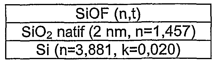
- the refractive index at 25 ° C of the SiO x F y layers obtained for ⁇ 632 nm was determined from the ellipsometric spectra;
- the presence or absence of water in the SiO x Fy layer was also determined by the presence or absence of a peak between 3400 and 3600 cm ⁇ 1 in the infrared spectra of this layer.
- the index increases from 1.40 to 1.46 (Si ⁇ 2 index) over 1 month, while for the protected layers according to the invention the index does not change during at least several months.
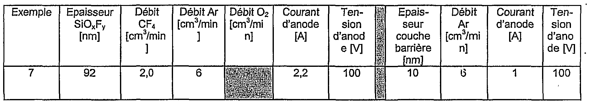
- Example 7 is an example of an anti-reflective coating which it is possible to produce with the layers of SiO x F y / Si ⁇ 2 of the invention.
- the substrate on which this antireflection coating has been produced is an Orma® substrate (material based on diallyl carbonate of diethylene glycol) coated with an abrasion-resistant varnish of the epoxysilane hydrolyzate type.
- the abrasion-resistant varnish used was obtained by dropping 80.5 parts of 0.1 N HCl drop by drop into a solution containing 224 parts of ⁇ -glycidoxypropyltrimethoxysilane and 120 parts of dimethyldiethoxysilane. The hydrolyzed solution is stirred for 24 hours at room temperature and then 718 parts of colloidal silica at 30% in methanol, 15 parts of aluminum acetylacetonate and 44 parts of ethylcellosolve are added.
- the substrate coated with varnish is subjected to a precooking for 15 minutes at 60 ° C. and then is passed through an oven at 100 ° C. for 3 hours.
- Example 7 consists of a stack of layers, starting from the upper layer up to the lower layer in contact with the substrate, which comprises:
- This coating has an Rm of 0.5 and an Rv (as defined in ISO WD 8930-4 cited above) of 0.4.
- SiO x F y and SiO 2 IAD layers were produced as described previously with the following operating conditions.
- the other layers of the stack are deposited in the vapor phase, under conditions conventional for those skilled in the art.
- FIG. 4 is a graph of the coefficient of reflection of the surface of the substrate as a function of the wavelength, after deposition of the coating of Example 7 and of a commercial CRIZAL® anti-reflection coating formed on an identical substrate.
- FIG. 5 is a graph of the reflection coefficient as a function of the wavelength of the coating of Example 7, after deposition, 20 days after deposition and 3 months after deposition.
- the curve in solid lines represents the reflection coefficient as a function of the wavelength of a coating similar to that of Example 7, but obtained by modeling according to conventional techniques known to those skilled in the art. 'art.
- the anti-reflective coating according to the invention has excellent stability over time, comparable to that of conventional coatings.
- nx10 stroke test is described in patent application WO / 9949097. Briefly, a fabric is applied to the surface of the anti-reflective treated glass and an eraser is pressed against the fabric. The rubber and the substrate are then moved relative to each other in a reciprocating movement, a cycle represents 10 reciprocating movements. The result represents the number of cycles that an anti-reflective glass can withstand before a defect appears.
- the refractive index is measured by ellipsometry on flat silicon disks.
- a SENTECH SE 400 ellipsometer was used, which is calibrated by the company SENTECH.
- the measurements were carried out with a wavelength of 632.8 nm at an angle of incidence of 70 °.
- the refractive index and the thickness are calculated from tan ⁇ and cos ⁇ by a two-dimensional Newton method, using the following model:
- a SOPRA GESP 5 VASE variable angle ellipsometer is used, the device is calibrated according to the procedure recommended by SOPRA.
- the tan ⁇ and cos ⁇ spectra are measured between 300 and 850 nm, for 3 angles of incidence, 65 °, 70 ° and 75 °.
- Levenberg-Marquardt regression method we make a global adaptation on 3 spectra using the following model:
- optical performances are determined by the commercial software FILM STAR DESIGN from FTG Software Associates - Princetown New Jersey and are given below.
- the optical performance of these stacks can also be determined without the contribution of the above software, by simple calculation, by following the basic principles of thin film optics, known to those skilled in the art and more particularly explained in the book "Thin film optical filters” Adam Higer Ltd - Bristol 1969 HA Me Loed - Professor of Optical Sciences - University of Arizona - Tuckson.
- the thicknesses of the layers are, in the absence of an indication to the contrary, mentioned in nanometers (nm).
- the refractive indices are the indices at 550 nm, 25 ° C.
- Examples 8 to 10 illustrate three stacks antireflection according to the invention deposited on a glass ORMA ®, based CR39 ®.
- Stacks are described starting from the lower layer, in contact with the substrate up to the upper layer (B1 - protective layer).
- Examples 18 to 24 illustrate the anti-reflection stacks of the same type as those described in Examples 11 to 17, but using as layer low index, last layer deposited a layer of SiOxFy of lower index (layer N).
- the thickness of the barrier layer is varied.
- Examples 29 to 31 describe anti-reflection stacks comprising 6 layers and a protective layer, the last layer of the deposit.
- another mode of deposition of the protective layer of metal oxide or of silicon oxide or also of the SiOxFy layer is a sputtering or sputtering deposition followed by an oxidation or oxidation in the presence of a fluorinated gas.
- the metal oxide or silicon layer is deposited by successively carrying out:
- steps 1) of deposition and 2) of oxidation are carried out in two locally distinct treatment zones.
- the technique of spraying the thin metallic or silicon layer [step 1)] is generally a continuous discharge (sputtering) and is carried out under vacuum.
- the target, or cathode, composed of the material (metal or silicon) to be deposited is supplied by a DC generator of several kV.
- the substrate to be coated is placed on an anode, facing the target cooled by circulation of water.
- a gas most often Argon
- a negative voltage is applied to the target to prime the plasma.
- the impact of the ions also causes the ejection of a few electrons called secondary electrons which are accelerated and collide with the atoms of the gas, which makes it possible to maintain the plasma.
- the atoms of the target once ejected will deposit on the substrate and thus create a thin layer.
- a magnetron cathode is used.
- These cathodes are diode type cathodes in which a magnetic field constitutes an electron trap. Electronic currents move in a direction that is both perpendicular to the electric field and the magnetic field along paths that are cycloidal. They therefore acquire greater energy, and above all travel much greater distances than in the continuous diode technique. The ionizing collisions will therefore be more numerous, therefore the ion current densities on the target also greater.
- magnetrons are more particularly described in the book “Handbook of deposition technologies for films and coatings” Science, Technology and Applications, Rointan F. Bunshah 2 nd Edition 1994 pp 280-292.
- an oxygen plasma or an oxygen-fluorinated gas mixture for example CF
- the oxygen plasma dissociates the molecules into oxygen atoms which are very reactive.
- the creation of reactive oxygen promotes the oxidation of the substrate.
- An example of a preferred sputtering process is OCLI's Metamode TM process, which combines all of the features described above, and the block diagram of which is shown in Figure 5. Referring to Figure 5, l obtaining a layer of metal oxide by the Metamode ® process is done in two separate chambers, namely a cathode sputtering chamber 1 or the metal of the cathode 3 is sprayed on the lens 4 placed on a plate 5 placed on a turntable 6. The deposition of the metal layer is done as described above.
- the lens 4 coated with a metal layer is brought into the oxidation chamber 2.
- an oxygen (or oxygen) plasma is created and a fluorinated gas such as CF if we want to obtain an oxyfluoride such as SiOxFy) to produce the layer of metal oxide or silicon.
- the metal sputtering / oxidation sputtering cycle is repeated as many times as necessary to obtain the desired thickness for the final layer of metal oxide or of SiO 2 .
- the sputtering of metal / oxidation sputtering cycle can be repeated by changing the nature of the sputtered metal so as to produce a stack of layers of metal oxides of different natures, for example for making an anti-reflection stack.
- the Metamode ® process can be implemented with a spraying device such as the Applied Vision RFX10 device shown diagrammatically, in view from below, in FIG. 6.
- the apparatus comprises two cathode sputtering chambers 1, 2 each provided with an inert gas inlet, for example argon, and a reaction chamber 3 (oxidation or oxyfluorination) provided with a gas supply (oxygen or mixture of oxygen and a fluorinated gas such as CF).
- the chambers are connected to a vacuum system (not visible in Figure 6).
- the substrates to be coated are placed on trays and are brought to the rotating plate 4 of the device via a loading airlock 5.
- the device also includes vacuum control means 6, such as that a Penning gauge and control and command means 7 of the sputtering and oxidation conditions.
- the substrates to be coated introduced by the loading lock, are brought by means of the turntable 4 into the sputtering chamber 1 or 2 where they are coated with a layer of metal or silicon as described above. After deposition of the metal or silicon layer, the substrates are brought into the reaction chamber 3 to carry out the oxidation or oxyfluorination of the metal or silicon layer. At the end of the treatment, the coated substrates are discharged through the airlock 5.
- Plasma gun power oxygen plasma: 100 W
- Ar flow (for Si sputtering): 12 sccm Flow 0 2 : 4 sccm
- CF flow 2 sccm P: 3m Tor (0.4 Pa)
- Ar flow (for Si spraying): 12 sccm Flow 0 2 : 4 sccm CF 4 flow: -
- the deposition is stopped for -30 s to ensure that there is no longer any CF 4 in the system.
Abstract
Description


Claims
Priority Applications (5)
| Application Number | Priority Date | Filing Date | Title |
|---|---|---|---|
| DE60326959T DE60326959D1 (en) | 2002-08-08 | 2003-08-07 | METHOD FOR THE PRODUCTION OF A THIN LAYER OF STABILIZED FLUOROUS SILICA, SUBSTRATE COATED THEREFOR, AND OPHTHALMIC LENS THUS OBTAINED THEREFOR |
| AU2003285355A AU2003285355B2 (en) | 2002-08-08 | 2003-08-07 | Method for obtaining a thin, stabilized fluorine-doped silica layer, resulting thin layer and use thereof in ophthalmic optics |
| JP2004528590A JP4434949B2 (en) | 2002-08-08 | 2003-08-07 | Methods for obtaining thin, stable, fluorine-doped silica layers, the resulting thin layers, and their application in ophthalmic optics |
| US10/523,951 US20060023311A1 (en) | 2002-08-08 | 2003-08-07 | Method for obtaining a thin, stabilized fluorine-doped silica layer, resulting thin layer, and use thereof in ophthalmic optics |
| EP03756536A EP1529124B1 (en) | 2002-08-08 | 2003-08-07 | Method for obtaining a thin, stabilized fluorine-doped silica layer, resulting coated substrat and ophthalmic lensoptics thus obtained |
Applications Claiming Priority (4)
| Application Number | Priority Date | Filing Date | Title |
|---|---|---|---|
| FR0210110 | 2002-08-08 | ||
| FR0210112A FR2843407B1 (en) | 2002-08-08 | 2002-08-08 | PROCESS FOR OBTAINING A THIN, STABILIZED, FLUORINE DOPED SILICA LAYER, THIN LAYER OBTAINED AND THEIR APPLICATION IN OPTICAL OPTICS |
| FR0210112 | 2002-08-08 | ||
| FR0210110A FR2843406A1 (en) | 2002-08-08 | 2002-08-08 | Production of a stabilized thin layer of silica doped with silica oxyfluoride for ophthalmic applications by vapor phase deposition of a protective layer of silica or metal oxide with ionic bombardment |
Publications (2)
| Publication Number | Publication Date |
|---|---|
| WO2004016822A2 true WO2004016822A2 (en) | 2004-02-26 |
| WO2004016822A3 WO2004016822A3 (en) | 2004-04-08 |
Family
ID=31889633
Family Applications (1)
| Application Number | Title | Priority Date | Filing Date |
|---|---|---|---|
| PCT/FR2003/002487 WO2004016822A2 (en) | 2002-08-08 | 2003-08-07 | Method for obtaining a thin, stabilized fluorine-doped silica layer, resulting thin layer and use thereof in ophthalmic optics |
Country Status (7)
| Country | Link |
|---|---|
| US (1) | US20060023311A1 (en) |
| EP (1) | EP1529124B1 (en) |
| JP (1) | JP4434949B2 (en) |
| KR (1) | KR101151813B1 (en) |
| AT (1) | ATE427367T1 (en) |
| DE (1) | DE60326959D1 (en) |
| WO (1) | WO2004016822A2 (en) |
Cited By (3)
| Publication number | Priority date | Publication date | Assignee | Title |
|---|---|---|---|---|
| JP2007041292A (en) * | 2005-08-03 | 2007-02-15 | Konica Minolta Opto Inc | Optical element |
| FR2965820A1 (en) * | 2010-10-12 | 2012-04-13 | Essilor Int | ARTICLE COMPRISING A MESOPOROUS LAYER PROTECTED BY A SEBUM BARRIER COATING AND METHOD OF MANUFACTURE |
| US9488852B2 (en) | 2010-12-10 | 2016-11-08 | Essilor International (Compagnie Generale D'optique) | Optical article comprising an antireflective coating with a low reflection both in the ultraviolet region and in the visible region |
Families Citing this family (16)
| Publication number | Priority date | Publication date | Assignee | Title |
|---|---|---|---|---|
| US6355580B1 (en) | 1998-09-03 | 2002-03-12 | Micron Technology, Inc. | Ion-assisted oxidation methods and the resulting structures |
| FR2859487B1 (en) * | 2003-09-04 | 2006-12-15 | Essilor Int | METHOD FOR DEPOSITING AN AMORPHOUS LAYER CONTAINING MAJORITARILY FLUORINE AND CARBON AND DEVICE SUITABLE FOR ITS IMPLEMENTATION |
| RU2455387C2 (en) * | 2006-03-31 | 2012-07-10 | Хойа Корпорейшн | Ion gun system, vapour deposition apparatus and method of making lens |
| FR2917510B1 (en) | 2007-06-13 | 2012-01-27 | Essilor Int | OPTICAL ARTICLE COATED WITH ANTIREFLECTIVE COATING COMPRISING A PARTIALLY FORMED UNDER-LAYER WITH ION ASSISTANCE AND METHOD OF MANUFACTURE |
| WO2009062140A2 (en) * | 2007-11-08 | 2009-05-14 | Sager Brian M | Improved anti-reflective coating |
| CN102084025B (en) * | 2008-09-05 | 2013-12-04 | 新柯隆株式会社 | Film-forming method and oil repellent base |
| JP4688230B2 (en) * | 2008-10-09 | 2011-05-25 | 株式会社シンクロン | Deposition method |
| CA2793855A1 (en) * | 2010-03-22 | 2011-09-29 | Luxottica Us Holdings Corporation | Ion beam assisted deposition of ophthalmic lens coatings |
| KR20130061683A (en) | 2010-04-29 | 2013-06-11 | 바텔리 메모리얼 인스티튜트 | High refractive index composition |
| WO2013152031A1 (en) * | 2012-04-04 | 2013-10-10 | Kla-Tencor Corporation | Protective fluorine-doped silicon oxide film for optical components |
| US20140272295A1 (en) * | 2013-03-14 | 2014-09-18 | Sdc Technologies, Inc. | Anti-fog nanotextured surfaces and articles containing the same |
| AU2013393576B2 (en) * | 2013-07-05 | 2018-10-04 | Essilor International | Optical article comprising an antireflective coating with a very low reflection in the visible region |
| TWI559026B (en) * | 2015-06-24 | 2016-11-21 | 財團法人工業技術研究院 | Anti-reflection strcuture and method of forming the same |
| FR3045672B1 (en) * | 2015-12-18 | 2018-03-16 | Corporation De L'ecole Polytechnique De Montreal | ARTICLE COMPRISING AN ORGANIC-INORGANIC LAYER OF LOW REFRACTIVE INDEX |
| JP2019015764A (en) * | 2017-07-03 | 2019-01-31 | 東海光学株式会社 | Plastic optical product, plastic spectacle lens and spectacles |
| EP3693765B1 (en) * | 2019-02-05 | 2023-04-19 | Essilor International | Article coated with an antireflective coating having improved optical properties |
Citations (2)
| Publication number | Priority date | Publication date | Assignee | Title |
|---|---|---|---|---|
| EP0975017A2 (en) * | 1998-07-22 | 2000-01-26 | Siemens Aktiengesellschaft | Silicon oxynitride cap for fluorinated silicate glass film in intermetal dielectric semiconductor fabrication |
| WO2002011195A1 (en) * | 2000-08-01 | 2002-02-07 | Essilor International Compagnie Generale D'optique | Method for depositing a fluorine-doped silica film |
Family Cites Families (8)
| Publication number | Priority date | Publication date | Assignee | Title |
|---|---|---|---|---|
| JPH03202461A (en) * | 1989-12-29 | 1991-09-04 | Nissin Electric Co Ltd | Formation of highly insulating thin silicon oxide film |
| JPH05215929A (en) * | 1992-02-03 | 1993-08-27 | Hitachi Cable Ltd | Manufacture of glass waveguide |
| US5719705A (en) * | 1995-06-07 | 1998-02-17 | Sola International, Inc. | Anti-static anti-reflection coating |
| US6001728A (en) * | 1996-03-15 | 1999-12-14 | Applied Materials, Inc. | Method and apparatus for improving film stability of halogen-doped silicon oxide films |
| JP3836214B2 (en) * | 1997-05-12 | 2006-10-25 | 凸版印刷株式会社 | Antireflection material and optical member |
| JPH11264903A (en) * | 1998-03-17 | 1999-09-28 | Canon Inc | Antireflection film and its production |
| US6165915A (en) * | 1999-08-11 | 2000-12-26 | Taiwan Semiconductor Manufacturing Company | Forming halogen doped glass dielectric layer with enhanced stability |
| US6511923B1 (en) * | 2000-05-19 | 2003-01-28 | Applied Materials, Inc. | Deposition of stable dielectric films |
-
2003
- 2003-08-07 EP EP03756536A patent/EP1529124B1/en not_active Expired - Lifetime
- 2003-08-07 US US10/523,951 patent/US20060023311A1/en not_active Abandoned
- 2003-08-07 AT AT03756536T patent/ATE427367T1/en not_active IP Right Cessation
- 2003-08-07 JP JP2004528590A patent/JP4434949B2/en not_active Expired - Fee Related
- 2003-08-07 WO PCT/FR2003/002487 patent/WO2004016822A2/en not_active Application Discontinuation
- 2003-08-07 DE DE60326959T patent/DE60326959D1/en not_active Expired - Lifetime
- 2003-08-07 KR KR1020057002555A patent/KR101151813B1/en active IP Right Grant
Patent Citations (2)
| Publication number | Priority date | Publication date | Assignee | Title |
|---|---|---|---|---|
| EP0975017A2 (en) * | 1998-07-22 | 2000-01-26 | Siemens Aktiengesellschaft | Silicon oxynitride cap for fluorinated silicate glass film in intermetal dielectric semiconductor fabrication |
| WO2002011195A1 (en) * | 2000-08-01 | 2002-02-07 | Essilor International Compagnie Generale D'optique | Method for depositing a fluorine-doped silica film |
Non-Patent Citations (3)
| Title |
|---|
| LEE J H ET AL: "INHOMOGENEOUS REFRACTIVE INDEX OF SIOXFY THIN FILMS PREPARED BY IONBEAM ASSISTED DEPOSITION" SURFACE AND COATINGS TECHNOLOGY, ELSEVIER, AMSTERDAM, NL, vol. 128/129, juin 2000 (2000-06), pages 280-285, XP000997583 ISSN: 0257-8972 * |
| PATENT ABSTRACTS OF JAPAN vol. 017, no. 654 (P-1653), 3 décembre 1993 (1993-12-03) & JP 05 215929 A (HITACHI CABLE LTD), 27 août 1993 (1993-08-27) * |
| PATENT ABSTRACTS OF JAPAN vol. 1999, no. 14, 22 décembre 1999 (1999-12-22) & JP 11 264903 A (CANON INC), 28 septembre 1999 (1999-09-28) * |
Cited By (7)
| Publication number | Priority date | Publication date | Assignee | Title |
|---|---|---|---|---|
| JP2007041292A (en) * | 2005-08-03 | 2007-02-15 | Konica Minolta Opto Inc | Optical element |
| FR2965820A1 (en) * | 2010-10-12 | 2012-04-13 | Essilor Int | ARTICLE COMPRISING A MESOPOROUS LAYER PROTECTED BY A SEBUM BARRIER COATING AND METHOD OF MANUFACTURE |
| WO2012049420A2 (en) | 2010-10-12 | 2012-04-19 | Essilor International (Compagnie Generale D'optique) | Item comprising a mesoporous layer protected by a coating acting as a barrier to the sebum, and production method |
| WO2012049420A3 (en) * | 2010-10-12 | 2012-08-30 | Essilor International (Compagnie Generale D'optique) | Item comprising a mesoporous layer protected by a coating acting as a barrier to the sebum, and production method |
| US9488852B2 (en) | 2010-12-10 | 2016-11-08 | Essilor International (Compagnie Generale D'optique) | Optical article comprising an antireflective coating with a low reflection both in the ultraviolet region and in the visible region |
| US10073279B2 (en) | 2010-12-10 | 2018-09-11 | Essilor International | Optical article comprising an antireflective coating with a low reflection both in the ultraviolet region and in the visible region |
| US10649232B2 (en) | 2010-12-10 | 2020-05-12 | Essilor International | Optical article comprising an antireflective coating with a low reflection both in the ultraviolet region and in the visible region |
Also Published As
| Publication number | Publication date |
|---|---|
| KR101151813B1 (en) | 2012-06-01 |
| EP1529124A2 (en) | 2005-05-11 |
| WO2004016822A3 (en) | 2004-04-08 |
| US20060023311A1 (en) | 2006-02-02 |
| ATE427367T1 (en) | 2009-04-15 |
| JP4434949B2 (en) | 2010-03-17 |
| KR20050062535A (en) | 2005-06-23 |
| JP2005534995A (en) | 2005-11-17 |
| DE60326959D1 (en) | 2009-05-14 |
| AU2003285355A1 (en) | 2004-03-03 |
| EP1529124B1 (en) | 2009-04-01 |
Similar Documents
| Publication | Publication Date | Title |
|---|---|---|
| EP1529124B1 (en) | Method for obtaining a thin, stabilized fluorine-doped silica layer, resulting coated substrat and ophthalmic lensoptics thus obtained | |
| US8263172B2 (en) | Method for producing optical element having multi-layered film | |
| EP0601928B1 (en) | Process for the treatment of metal oxide or nitride thin films | |
| EP1641720A2 (en) | Dielectric-layer-coated substrate and installation for production thereof | |
| EP1232407A2 (en) | Heat-absorbing filter and method for making same | |
| JP6381687B2 (en) | Method for forming durable MgO-MgF2 composite film for infrared light antireflection coating | |
| EP1135335A1 (en) | Thin hafnium oxide film and method for depositing same | |
| EP1307907B1 (en) | Method for depositing a fluorine-doped silica film | |
| Wolfe et al. | Deposition of durable wideband silver mirror coatings using long-throw low-pressure DC-pulsed magnetron sputtering | |
| JP2005133131A (en) | Method for forming refractive-index-changing layer | |
| FR2843406A1 (en) | Production of a stabilized thin layer of silica doped with silica oxyfluoride for ophthalmic applications by vapor phase deposition of a protective layer of silica or metal oxide with ionic bombardment | |
| EP2744760B1 (en) | Antireflection glazing unit equipped with a porous coating and method of making | |
| EP2045352A1 (en) | Method of obtaining a hard surface on the nanometric scale | |
| Devasahayam et al. | Material properties of ion beam deposited oxides for the optoelectronic industry | |
| JP5665751B2 (en) | Hafnium oxide-coating | |
| FR2843407A1 (en) | Production of a stabilized thin layer of silica doped with silica oxyfluoride for ophthalmic applications, by vapor phase deposition of a protective layer of silica or metal oxide with ionic bombardment | |
| Volpian et al. | Nanogradient optical coatings | |
| EP0963457A1 (en) | Method for preparing thin films of fluorinated compounds | |
| CN114196924A (en) | Coating method of vacuum ultraviolet aluminum reflector on surface of copper substrate | |
| JP2001108802A (en) | Antireflection film | |
| Lee et al. | Optimization of high and anti-reflective facet coating for near infrared high power laser diode | |
| Abromavičius et al. | Optimization of HfO2, Al2O3 and SiO2 deposition leading to advanced UV optical coatings with low extinction | |
| FR3009563A1 (en) | MAGNETRON CATHODIC SPRAY METHOD COMPRISING A PRIOR IN SITU ABRASION STEP |
Legal Events
| Date | Code | Title | Description |
|---|---|---|---|
| AK | Designated states |
Kind code of ref document: A2 Designated state(s): AE AG AL AM AT AU AZ BA BB BG BR BY BZ CA CH CN CO CR CU CZ DE DK DM DZ EC EE ES FI GB GD GE GH GM HR HU ID IL IN IS JP KE KG KP KR KZ LC LK LR LS LT LU LV MA MD MG MK MN MW MX MZ NI NO NZ OM PG PH PL PT RO RU SC SD SE SG SK SL SY TJ TM TN TR TT TZ UA UG US UZ VC VN YU ZA ZM ZW |
|
| AL | Designated countries for regional patents |
Kind code of ref document: A2 Designated state(s): GH GM KE LS MW MZ SD SL SZ TZ UG ZM ZW AM AZ BY KG KZ MD RU TJ TM AT BE BG CH CY CZ DE DK EE ES FI FR GB GR HU IE IT LU MC NL PT RO SE SI SK TR BF BJ CF CG CI CM GA GN GQ GW ML MR NE SN TD TG |
|
| 121 | Ep: the epo has been informed by wipo that ep was designated in this application | ||
| WWE | Wipo information: entry into national phase |
Ref document number: 2003756536 Country of ref document: EP |
|
| ENP | Entry into the national phase |
Ref document number: 2006023311 Country of ref document: US Kind code of ref document: A1 |
|
| WWE | Wipo information: entry into national phase |
Ref document number: 10523951 Country of ref document: US Ref document number: 2004528590 Country of ref document: JP |
|
| WWE | Wipo information: entry into national phase |
Ref document number: 1020057002390 Country of ref document: KR |
|
| WWE | Wipo information: entry into national phase |
Ref document number: 1020057002555 Country of ref document: KR |
|
| WWE | Wipo information: entry into national phase |
Ref document number: 2003285355 Country of ref document: AU |
|
| WWE | Wipo information: entry into national phase |
Ref document number: 20038239000 Country of ref document: CN |
|
| WWP | Wipo information: published in national office |
Ref document number: 2003756536 Country of ref document: EP |
|
| WWR | Wipo information: refused in national office |
Ref document number: 1020057002390 Country of ref document: KR |
|
| WWW | Wipo information: withdrawn in national office |
Ref document number: 1020057002390 Country of ref document: KR |
|
| WWP | Wipo information: published in national office |
Ref document number: 1020057002555 Country of ref document: KR |
|
| WWP | Wipo information: published in national office |
Ref document number: 10523951 Country of ref document: US |