WO1998022779A2 - Backscatter error reducer for interferometric fiber optic gyroscope - Google Patents
Backscatter error reducer for interferometric fiber optic gyroscope Download PDFInfo
- Publication number
- WO1998022779A2 WO1998022779A2 PCT/US1997/019260 US9719260W WO9822779A2 WO 1998022779 A2 WO1998022779 A2 WO 1998022779A2 US 9719260 W US9719260 W US 9719260W WO 9822779 A2 WO9822779 A2 WO 9822779A2
- Authority
- WO
- WIPO (PCT)
- Prior art keywords
- light
- waves
- backscatter
- modulation signal
- error
- Prior art date
Links
Classifications
-
- G—PHYSICS
- G01—MEASURING; TESTING
- G01C—MEASURING DISTANCES, LEVELS OR BEARINGS; SURVEYING; NAVIGATION; GYROSCOPIC INSTRUMENTS; PHOTOGRAMMETRY OR VIDEOGRAMMETRY
- G01C19/00—Gyroscopes; Turn-sensitive devices using vibrating masses; Turn-sensitive devices without moving masses; Measuring angular rate using gyroscopic effects
- G01C19/58—Turn-sensitive devices without moving masses
- G01C19/64—Gyrometers using the Sagnac effect, i.e. rotation-induced shifts between counter-rotating electromagnetic beams
- G01C19/72—Gyrometers using the Sagnac effect, i.e. rotation-induced shifts between counter-rotating electromagnetic beams with counter-rotating light beams in a passive ring, e.g. fibre laser gyrometers
Definitions
- the present invention pertains to interferometric fiber optic gyroscopes (IFOGs), and particularly to IFOGs having backscatter error sources in the optical fiber sensing loop and in the integrated optical circuit (IOC) which incorporates a light beam splitter and combiner, and at least one phase modulator. More particularly, the present invention pertains to the reduction of one kind of backscatter error.
- IFOGs interferometric fiber optic gyroscopes
- IOC integrated optical circuit
- Two types of backscatter error mechanisms are interference between the primary wave and backscattered wave and interference between the two counter-propagating backscattered waves or secondary waves at the gyroscope output at the photodetector.
- the former has been considered the fundamental IFOG backscatter error mechanism, and therefore has been studied in some detail.
- many commonly employed design features i.e., short coherence light sources, bias modulation at the proper frequency, loop coupler having a near 50/50 splitting ratio and a demodulator having good quadrature rejection
- the latter backscatter error mechanism has been considered a second order effect, which is of significant concern in high accuracy IFOGs, and thus has not been rigorously dealt with to date.
- the present invention is a solution to the second order backscatter error problems in an interferometric fiber optic gyroscope.
- the solution is a backscatter error reducer for an interferometric fiber optic gyroscope having at least one phase modulator for receiving at least two phase modulation signals.
- One signal is the bias phase modulation and the other is a carrier suppression phase modulation.
- the bias modulation signal is for normal operation.
- the carrier phase modulation signal has an amplitude such that the modulator generates at least one radian of phase difference between the two sets of secondary waves to reduce the interference between the two sets of backscatter or secondary waves of light originating in the Sagnac loop of the gyroscope.
- BRIEF DESCRIPTION OF THE DRAWING Figure 1 shows a basic interferometric gyroscope and the Rayleigh backscatter wave paths.
- Figure 2 is a graph that shows how much backscatter contributes to net error of the gyroscope rotation rate indication, relative to location in the Sagnac loop where the backscatter originates.
- Figure 3 where the rotation rate error depends on the absolute value of the Bessel function, reveals a graph of the Bessel function relative to amplitude difference of the at least two phase modulations of the light beams in the gyroscope.
- Figure 4 shows a plot of backscatter error for the situations where no carrier suppression modulation is applied, one carrier suppression modulation frequency is eight times the proper frequency, and two carrier suppression modulations have frequencies at eight and ten times the proper frequency, respectively.
- Figure 5 is a plot of backscatter error reduction versus suppression modulation depth.
- Figure 6 shows plots of relative quadrature versus position for no suppression modulation and for two suppression modulation and for two suppression modulations.
- Figure 7 is a plot of the unwanted sinusoidal rate signal of a gyroscope using carrier suppression at frequencies 10 Hz off of even multiples of the proper frequency.
- Figure 8 shows the Rayleigh backscatter wave paths in an integrated optics circuit.
- Figure 9 plots the net error signal due to backscatter in the waveguides of the integrated optic circuit.
- Figure 10 shows an integrated optic circuit having carrier suppression modulators.
- Figure 11 is a plot that indicates that carrier suppression cannot be achieved simultaneously at all points along the suppression modulator.
- Figure 12 is a plot of relative backscatter as a function of carrier suppression modulation amplitude.
- Figure 13 is a configuration of an integrated optics circuit and modulators involving square wave bias modulation.
- Figures 14a, 14b and 14c reveal the interaction of the carrier suppression phase modulation signal with the bias phase modulation signal.
- Figure 15 shows a sinusoidal optical signal produced by phase modulation for carrier suppression of backscatter in an open loop gyroscope under no rotation.
- Figure 16 is a plot of rotation error versus the difference in frequencies of the carrier suppression phase modulation and the bias phase modulation.
- Figure 17 shows plots of rotation rate error and angle random walk, respectively, versus the difference in frequencies of the carrier suppression phase modulation and the bias phase modulation.
- Eb' s p W are assumed to originate from a pair of fiber sections 16 and 18 having a length equal to the coherence length L c of a light source 14 and at a location in the fiber loop 12 having an index p .
- the scattered fields ⁇ bs,l,p ⁇ and ⁇ bs,2,p ⁇ at the y-junction input/output are: i[ ⁇ t+ ⁇ (.))
- a is the lumped optical loss from the input/output to scattering section 16 or 18, ⁇ is the angular frequency of source 14, ⁇ m is the amplitude of the bias phase modulation from generator 23, applied to one of the primary waves, ⁇ m is the bias modulation frequency, and p is the transit time from the scattering sections 16 and 18 to y-j unction 20.
- the amplitude E bs of the scattered fields is assumed to be constant with time and the same for all scattering sections like those of sections 16 and 18.
- the intensity ⁇ bs,p ⁇ of the interfering scattered waves is
- I bs , p (t) 2aI bs ⁇ + co ⁇ 2 ⁇ m cos( ⁇ m ⁇ p ) sm( ⁇ m t - ⁇ m ⁇ p ) + A ⁇ p (t) ⁇ . (6)
- Equation 7 Expanding the terms in Equation 7 as a series of Bessel functions and using Equation 6, we find that the second term in Equation 7 represents in-phase and quadrature error signals that are synchronous with the bias modulation and have the frequency ⁇ m .
- the amplitude of the in-phase error signal is
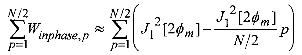
- Equation 8 represents the error signal due to light scattering from only one pair of scattering sections 16 and 18. To find the net error I e rr,si g due to all scattering section pairs, one takes the root-sum-square of the peak amplitudes of for all p.
- the peak amplitude (denoted by ybs,sig,p ) ) is
- N is the number of pairs of scattering sections that fit within fiber loop 12 of length L
- Equation 11 Using Equations 8, 10 and 12, one can rewrite Equation 11 as
- Equation 14 determines how much a particular pair of scattering sections contribute to the net error I e rr,si g ⁇
- a plot 24 of this function shown in Figure 2 shows that backscatter originating near IOC 21 contributes more to the net error then backscatter originating from the center of fiber loop 12.
- This error model does not include weighting effects associated with distributed optical loss in the fiber, which will reduce W inphase p s a function of p . If these effects were included, then curve 24 in Figure 2 would be asymmetric about the center of fiber loop 12 and the area under the right-hand-side of curve 24 would be less than the area under the left-hand-side of curve 24.
- a plot of a linear function 25 is also shown in Figure 2 a plot of a linear function 25. The area under linear curve 25 approximates the area under W inphase p . The value of the summation in Equation 13 is proportional to the area under "actual" curve 24 in Figure 2.
- Equation 17 The summation in Equation 17 can be written as
- Equation 13 Equation 13
- the electric fields of the primary waves emanating from IOC 21 input/output are:
- Equation 29 shows that ⁇ err, fiber decreases with longer fiber lengths and sources with shorter coherence lengths.
- the rotation rate error is _ 1.55 x 10 ⁇ 6 x 3 x 10* m - s ⁇ l x 6.3 x lO "8 ⁇ "1 err 'f' ber ⁇ 2 ⁇ /2 ⁇ X 0.15m
- Equations 30 and 31 show that the rotation rate error due to Rayleigh backscatter from loop fiber 12 is more significant for a navigation grade IFOG operating at a source wavelength of 0.83 ⁇ m.
- the Rayleigh backscatter is significantly higher at this wavelength than at longer wavelengths.
- the present invention incorporates carrier suppression modulation to suppress backscatter errors in IFOGs.
- a sinusoidal phase modulation to one of two optical waves that is producing the backscatter
- the interference between the backscatter waves is "scrambled".
- the amplitude of the phase modulation is adjusted such that the carrier of the optical wave (optical energy occurring at the source, or baseband, frequency) is suppressed. Therefore, interference between the two backscatter waves will have frequency components at multiple integers of the carrier suppression modulation frequency and no interference will occur at the baseband frequency.
- the final result is that backscatter errors will be frequency shifted from baseband to multiple integers of the carrier suppression modulation frequency and will average to zero over time.
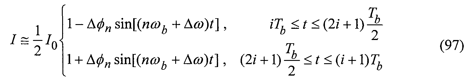
- the intensity ⁇ bs, p ⁇ due to the scattered waves is
- Equation 34 By expressing the terms in Equation 34 as a series of Bessel functions, one finds that the fourth term is the only term that has a signal that is synchronous with the bias modulation. From Equation 34 the in-phase error signal is found to be
- the frequency of the carrier suppression modulation can be set very low relative to the proper frequency or can be set near multiple integers of twice the proper frequency. If one considers the case where the carrier suppression modulation is at a frequency much less than the proper frequency then ⁇ s « ⁇ m . (37)
- the rotation rate error corresponding to low frequency carrier suppression is
- Equation 39 shows that ⁇ e r, fiber depends on the absolute value of the Bessel function
- Figure 4 shows numerical calculations of the function W inphase p V s. p for three cases: plot 28 for no carrier suppression modulation employed; plot 29 for one carrier suppression modulation employed at 8 times the proper frequency; and plot 30 for two carrier suppression modulations employed at 8 and 10 times the proper frequency.
- the bias modulation amplitude 2 ⁇ m was assumed to be 1.8 radians and the suppression modulation amplitude 2 ⁇ s was assumed to be 2.4 radians.
- the areas under curves 28, 29 and 30 are proportional to the backscatter error. The degree of relative error reduction is found by normalizing the areas under curves 29 and 30 to the area corresponding to no carrier suppression.
- FIG. 5 is a plot 31 of calculated backscatter error reduction vs. suppression modulation depth. Carrier suppression modulation frequency was assumed to be 8 times the proper frequency. Solid curve 31 shows that the backscatter error can not be reduced to near zero at a modulation amplitude of 2.4 radians. To obtain an error reduction factor of 3 or more, either a larger modulation depth must be used or two modulations must be employed.
- Figure 6 shows calculations of the quadrature backscatter error vs. position in the loop for two cases: a curve 32 for no carrier suppression modulation and a curve 33 for two carrier suppression modulations operating at 8 and 10 times the proper frequency.
- This plot shows that the quadrature error is less in magnitude than the in-phase error. Since this error is in quadrature, it is mostly rejected by the phase sensitive detector (PSD) that demodulates the rate signal, and is therefore insignificant compared to the in- phase error.
- PSD phase sensitive detector
- the plot also shows that the same suppression modulation used to reduce the in-phase error will also reduce the quadrature error. Since the quadrature error appears to be insignificant, it will no longer be considered in this analysis.
- a side effect of carrier suppression modulation an AC rate output error. Since the carrier suppression modulation produces a sinusoidal non-reciprocal phase modulation between the two main waves in the loop, it will generate an unwanted sinusoidal rate signal (AC rate).
- the frequency of the most significant AC rate signal, generated by a suppression modulation operating well below the proper frequency, will be mainly at the suppression modulation frequency.
- the frequency of the AC rate is not obvious.
- the amplitude of the AC rate corresponding to suppression modulation operating at low frequency will be calculated first.
- the electric fields of the main waves or primary waves at the input/output port ofIOC 21 are:
- the carrier suppression frequency is assumed to be much less than the bias modulation frequency ⁇ s « ⁇ m , (42) and therefore the following approximations are made:
- Equation 45 The cosine function in Equation 45 can be written as
- Equation 48 The second term on the right-hand side (RHS) of Equation 48 can be written as a series of Bessel functions
- Equation 49 shows that many AC rate signals are generated at odd multiple integers of the suppression modulation frequency. Since the amplitude of the AC rate signals diminishes for the higher frequencies, the most significant unwanted signal (represented by the first term on the RHS of Equation 49) occurs at the suppression modulation frequency. Using the first term on the RHS of Equation 49 and Equations 45 and 48, the AC intensity signal is found to be
- the AC rate at 10Hz is about
- the AC rate at 10Hz is about
- the random bias fluctuation (at an integration time of 2.8 x 10 hr ) of a high performance IFOG operating at a source wavelength of 1.55 ⁇ m is
- a comparison of the AC rate amplitude and the random bias fluctuations shows that the employment of low frequency carrier suppression modulation will cause the gyro to be out of bias specification at integration times of approximately one-half the AC rate period. Since the AC rate is induced by an applied phase modulation, it could be partially removed from the gyro output. However, the amplitude of the AC rate will depend on the optical and electrical gains of the system, and therefore will not be constant over time. To reduce the AC rate below the level of normal bias fluctuations would be an aggressive task. Furthermore for a closed loop system, the main feedback loop will cancel out an externally applied phase modulation. Therefore the carrier suppression modulation must be produced by "forcing" the main feedback loop to generate the phase modulation. This would greatly increase the complexity of the main feedback loop electronics.
- the AC rate amplitude is calculated for a relatively high suppression modulation frequency.
- the intensity due to the interference of the main waves is the intensity due to the interference of the main waves.
- Equation 61 represents an amplitude modulated signal that is synchronous with the bias modulation and has an envelope that occurs at the frequency ⁇ ⁇ when k - q - ⁇ .
- the amplitude-modulated signal is demodulated by the gyro electronics producing an unwanted AC output with an amplitude that is proportional to
- Equation 62 and 63 the AC rate is found to be ⁇ s ⁇ s ⁇ c J k _ ⁇ ( 2 ⁇ m ) ⁇ m 4LD J ⁇ (2 ⁇ m )
- the AC rate for the case of carrier suppression at high frequency is similar to the case of carrier suppression at low frequency except a factor of 1/2 and the ratio which can significantly reduce the AC rate.
- Figure 7 shows a plot 34 of calculated AC rate for a high performance IFOG employing carrier suppression at frequencies 10 Hz off even multiples of the proper frequency and at an amplitude of 2.4 radians.
- the index k refers to an even harmonic of the proper frequency.
- Plot 34 shows that the preferred operating frequency for the suppression modulation is near 8 times the proper frequency or greater. At these frequencies, the unwanted AC rate signal is reduce to levels below the normal bias fluctuations of the gyro output. Furthermore, by employing the carrier suppression modulation frequencies well above the bandwidth of the main feedback loop, the main loop is unaffected by the suppression modulation.
- FIG. 8 shows a diagram of integrated optics chip 21 and how the backscatter is modulated by bias modulation generator 23 and modulator 35.
- the backscatter wave traveling through bias modulator 35 is phase modulated with an amplitude ⁇ m i x p) that depends on the distance L mod traveled through the modulator 35.
- the electric fields of the scattered waves are:
- the net error signal I e rr,sig is the root-sum-square of the peak amplitudes corresponding to all backscattering pairs of IOC 21 waveguide sections 36 and 37.
- the net signal is
- L m is the length of the phase modulator 35.
- the amplitude of the backscatter phase modulation is assumed to be a linear function with p
- ⁇ m ,max is the amplitude of phase modulation for an optical wave making one full pass through phase modulator 35.
- the net error signal due to backscatter in IOC 21 waveguides 36 and 37 can be written as
- a plot of the function shows that the area under curve 40 can be approximated by the area under a linear function or fit curve 41.
- Equation 76 The approximation to the summation in Equation 76 is
- the value of backscatter per unit length of the fiber of coil 12 was obtained from experimental measurements made with a 1.55 ⁇ m Er-doped fiber light source 14. To estimate ⁇ chi p , the capture factor associated with fiber 12 is assumed to be the same for
- the electric fields associated with the scattered waves are: , , 1/2 ⁇ > ⁇ s( x p) s TM(a> s t)+ ⁇ ⁇ B (*
- the first term on the RHS of Equation 91 represents a signal that is synchronous with the bias modulation 23.
- the net error signal due to backscatter from all pairs of IOC 21 waveguide (36 and 37) sections is
- ⁇ s,max is the amplitude of carrier suppression phase modulation 45 for an optical wave making one full pass through phase modulator 42.
- p curve is numerically calculated and then normalized to the area of function associated with no carrier suppression.
- a plot 47 in Figure 12 shows that the backscatter error can not be reduced to zero at carrier suppression modulation 45 amplitude of about 2.4 radians when the modulation at ⁇ s is applied to phase modulator 42 located opposite to bias modulation 23 on modulator 43.
- a larger modulation depth can be used, or two carrier suppression modulations can be employed.
- Another IOC 21 design enhancement that will allow for greater reductions in backscatter error is a carrier suppression modulator 44 that is placed before the bias phase modulator 43, as shown by plot 48. In this case, the phase modulation amplitude of the scattered waves (that will coherently interfere with the scattered waves from the bias phase modulator
- the rotation rate error is then which can be eliminated when the modulation amplitude 2 ⁇ Sfinax is set to about 2.4 radians.
- An optical design change of the IFOG can also significantly reduce the error associated with backscatter in IOC 21.
- This change involves replacing the IOC Y- junction 20 with a fiber coupler, and placing IOC 21 phase modulators 42 and 44 such that the backscatter from IOC 21 waveguide 36 will only coherently interfere with backscattered light from fiber on the opposite side of the sensing loop 12. Since the backscattered light from a short section of fiber 12 is significantly less than the backscatter from IOC 21 waveguide 36, the amplitude of the interference between these two waves will be significantly smaller than the amplitude of the interference between two waves that are both backscattered in IOC 21 waveguide 36.
- carrier suppression modulation which involves applying one or more sinusoidal phase modulations to the light propagating through the integrated optics chip 21 of the IFOG.
- This technique is based on an IFOG sensor employing sinusoidal bias modulation.
- a high performance IFOG will most likely employ a square-wave bias modulation 50 of figure 13, an analog-to-digital converter (ADC) to sample the photodetector signal, and square-wave demodulation.
- ADC analog-to-digital converter
- Figures 14a, 14b and 14c show how the carrier suppression phase modulation 45 interacts with the bias phase modulation 50 while being converted into a optical intensity signal (intensity modulation) by the sagnac interferometer.
- the IFOG interferogram (Fig. 14b) shows how the intensity / (detected at the photodetector) varies with the phase difference A ⁇ between the counter-propagating light waves emanating from the Sagnac interferometer.
- the total phase modulation (Fig.
- optical intensity signal 54 shown between points b and c of Fig. 14c is not exactly a sign inverted version of optical intensity signal 55 shown between points a and b of Fig. 14c.
- a simple method of square demodulation consist of: (i) finding the average value for optical intensity signal 55 shown between points a and b of Fig. 14c and the average value for optical intensity signal 54 shown between points b and c of Fig. 14c, then (ii) finding the difference between the two average values. Under no rotation, the difference between the two average values should be zero. However, the sinusoidal part of the optical signals 54 and 55 do not have the same average, therefore will result in a non-zero demodulator output, which is a false indication of rotation.
- Sinusoidal signals 56 and 57 shown between points c and e of Fig. 14c
- Figure 15 illustrates how the demodulation process is modeled to quantitatively determine the rotation sensing error due to carrier suppression modulation.
- the typical demodulation process employed in IFOGs consist of sampling the photodetector signal with an analog-to-digital converter (ADC), then performing the signal processing with digital electronics. Not all of the samples are used in the demodulation process.
- the bias modulation 50 transitions between ⁇ ⁇ /2 causes sharp glitches (not shown in Fig. 15) in optical intensity signal 58 at times i b , iT b + T b /2 ⁇ iT b + T b , etc.
- samples 59 that occur during a gating time tg are not used in the demodulation process.
- Samples 60 between i b + t g and i b + T b j2 are summed to produce a value that is proportional to the average value of the signal corresponding to the first half cycle of the i bias modulation cycle.
- the demodulated signal (which is proportional to the rotation rate) is the difference between the two summed values.
- the demodulation process is performed for successive bias modulation cycles.
- the bias modulation is represented by the values ⁇ /2 and - ⁇ /2.
- a n is the amplitude of the sinusoidal phase modulation difference between the counter-propagating light waves, and the angular frequency of the sinusoidal modulation ( n ⁇ b + ⁇ ⁇ ) is shown to be some small difference A ⁇ away from the n harmonic (where n is even) of the bias modulation angular frequency a> b
- T b is the period of bias modulation 50 and i refers to which bias modulation cycle is being considered.
- the bias modulation 50 frequency is set exactly to the eigen frequency of the Sagnac interferometer.
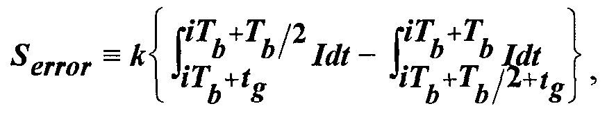
- the intensity signal is integrated piecewise for a part of each half period of the bias modulation 50. Since one assumes that there is no rotation, the demodulated signal is an error signal S error ,
- k is a constant that represents the gain of the photodetector and electronics up to and including the ADC.
- the integration limits include the partial sampling technique
- the first integral in Eq. 98 corresponds to the first half of the i* bias modulation cycle and the second integral corresponds to the second half of the i ⁇ bias modulation cycle.
- the time dependence of the error signal S error is found by using the index to model an arbitrary bias modulation 50 cycle.
- the intensity signal is integrated piecewise for a part of each half period of the bias modulation 50. Since one assumes that there is no rotation, the demodulated signal is an error signal S error ,
- & is a constant that represents the gain of the photodetector and electronics up to and including the ADC.
- the integration limits include the partial sampling technique (not using all the samples of the entire waveform) or gating time t g .
- the first integral in Eq. 98 corresponds to the first half of the / bias modulation cycle and the second integral corresponds to the second half of the bias modulation cycle.
- the time dependence of the error signal S error is found by using the index i to model an arbitrary bias modulation 50 cycle.
- the sampling ratio R s is defined as the number of samples taken (or used) during a half bias modulation 50 period, after the gating time tg , divided by the total possible number of samples that could be taken (or used) during a full half period of the bias modulation 50 cycle.
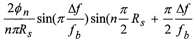
- Equation 102 shows that S error is an sinusoidal error signal that varies at a frequency of Af .
- the amplitude of the error signal is
- phase difference amplitude A ⁇ n due to a carrier suppression modulation 45 is a function of the suppression modulation 45 frequency and the eigen frequency f e ,
- ⁇ n is the phase modulation amplitude of the light wave making a single pass through phase modulator 42.
- the bias modulation 50 frequency was set to the eigen frequency.
- ⁇ rotation is the phase difference caused by the rotation.
- the demodulated signal is found by performing the following integration.
- Equation 110 shows how much rotation signal S rotation is generated by a phase difference A ⁇ rotation caused by rotation.
- the open-loop scale factor is all the coefficients within the brackets in Eq. 110.
- phase difference due to a rotation is given by
- Eq. 117 The design constraint shown in Eq. 117 can be satisfied by first setting R s by other design constraints, then setting n to satisfy Eq. 117 by choosing the appropriate carrier suppression frequency. If this is done, then Eq. 118 shows that ⁇ rotat i on error will approach zero very quickly when Af is adjusted towards zero.
- ARW angle random walk
- ARWC angle random walk coefficient
- ⁇ integration time for a cluster analysis.
- Cluster analysis is a common method used for determining the various types of error coefficients of a gyro.
- ⁇ rotat wn er ro r s insignificant if it is always less than AR W - F° r a cluster analysis, a sinusoidal error will have a maximum effect when the integration time is approximately 1/2 the period of the sinusoidal error.
- Figure 17 shows plots 63 and 64, respectively of ⁇ rot ⁇ t i o err o r n ⁇ ARW. max vs Af . Plots 63 and 64 show that ⁇ rotation error ⁇ ⁇ ARW, ax when Af ⁇ lSHz .
- Point 65 shows that Af should be less than 18 Hz so that ⁇ r0tat ion err o r 1S l ess m n the gyro noise output ⁇ AR W , max ⁇ Therefore, for this example, if carrier suppression frequency 45 is set to 16 times the bias modulation frequency 50 (which is at the eigen frequency) plus or minus 18Hz or less, then the sinusoidal rate error caused by carrier suppression modulation 45 will be less than the rate noise output of the IFOG. If one reduces Af to about 1Hz, then the sinusoidal error is about 100 times less than the rate noise output of the IFOG. At this level, the sinusoidal error should be insignificant for all systems using an IFOG employing carrier suppression modulation.
- Rayleigh backscatter from IOC 21 waveguides 36 and 37 may cause significant rotation sensing errors in IFOGs operating at all source 14 wavelengths.
- Navigation grade IFOGs operating near source 14 wavelengths of 0.83 ⁇ m may have significant rotation sensing errors due to backscatter from loop fiber 12.
- the backscatter error can be substantially reduced by applying a carrier suppression phase modulation 45 to one of the primary waves in loop 12. The manner in which the suppression modulation 45 is applied greatly determines overall performance of the error reduction technique.
- Suppression modulation 45 at a frequency much less than the proper frequency will generate an unwanted AC signal at the gyro output. Even though this signal could be subtracted from the output, it would be very difficult to reduce the AC signal below the level of normal random fluctuations of the gyro output. Suppression modulation 45 at a frequency that is near even multiple integers of the proper frequency will also generate an unwanted AC signal. However, the amplitude of the unwanted AC signal can be reduced below the level of normal gyro output fluctuations if the frequency of the suppression modulation 45 is set near even multiple integers of 8 or greater of the proper frequency.
- phase modulators 42, 43, 44, used for bias 23, 50 and suppression 45 modulation have a significant impact on the level of backscatter error reduction obtained with suppression modulation 45. If phase modulators 42 and 43 are on separate waveguides 36 and 37 and are placed opposite to each other, then suppression modulation 45 will reduce the backscatter error by about a factor of 10. To reduce the backscatter error by more than a factor of 10, two design enhancements can be employed: an additional suppression modulation at a different frequency can be applied, and/or a suppression phase modulator 44 can be placed before bias phase modulator 43.
- Optical time delays associated with the long loop 12 lengths also have a significant effect on the level of reduction of errors associated with backscatter from loop fiber 12. If the frequency of the suppression modulation 45 is set greater than the proper frequency, then suppression modulation 45 will reduce the backscatter error by about a factor of 5. To obtain a higher error reduction factor, multiple carrier suppression modulations at different frequencies can be used. Further, bias modulation 50 signal may be a square wave rather than a sine wave.
- the design criterion for an IFOG employing square-wave modulation/demodulation and carrier suppression modulation is that the ratio (nR s )/2 must be an integer and that Af must be small enough such that the sinusoidal rate error produced by the carrier suppression modulation 45 is less than the gyro random noise output at an integration time where the sinusoidal error has a maximum effect.
Abstract
Description


Claims
Priority Applications (4)
| Application Number | Priority Date | Filing Date | Title |
|---|---|---|---|
| CA002265594A CA2265594A1 (en) | 1996-10-31 | 1997-10-27 | Backscatter error reducer for interferometric fiber optic gyroscope |
| EP97954891A EP0935738B1 (en) | 1996-10-31 | 1997-10-27 | Backscatter error reducer for interferometric fiber optic gyroscope |
| JP52366198A JP4052676B2 (en) | 1996-10-31 | 1997-10-27 | Backscattering error reduction device for interference optical fiber gyroscope |
| DE69728416T DE69728416T2 (en) | 1996-10-31 | 1997-10-27 | RETURN CONTROL ERROR REDUCTION IN INTERFEROMETRIC OPTICAL GLASS FIBER GYROSCOPES |
Applications Claiming Priority (2)
| Application Number | Priority Date | Filing Date | Title |
|---|---|---|---|
| US08/741,464 US5781300A (en) | 1996-10-31 | 1996-10-31 | Backscatter error reducer for interferometric fiber optic gyroscope |
| US08/741,464 | 1996-10-31 |
Publications (2)
| Publication Number | Publication Date |
|---|---|
| WO1998022779A2 true WO1998022779A2 (en) | 1998-05-28 |
| WO1998022779A3 WO1998022779A3 (en) | 1998-08-20 |
Family
ID=24980823
Family Applications (1)
| Application Number | Title | Priority Date | Filing Date |
|---|---|---|---|
| PCT/US1997/019260 WO1998022779A2 (en) | 1996-10-31 | 1997-10-27 | Backscatter error reducer for interferometric fiber optic gyroscope |
Country Status (6)
| Country | Link |
|---|---|
| US (1) | US5781300A (en) |
| EP (1) | EP0935738B1 (en) |
| JP (1) | JP4052676B2 (en) |
| CA (1) | CA2265594A1 (en) |
| DE (1) | DE69728416T2 (en) |
| WO (1) | WO1998022779A2 (en) |
Families Citing this family (20)
| Publication number | Priority date | Publication date | Assignee | Title |
|---|---|---|---|---|
| US6175410B1 (en) * | 1998-12-17 | 2001-01-16 | Honeywell Inc. | Fiber optic gyroscope having modulated suppression of co-propagating and counter-propagating polarization errors |
| WO2000045532A1 (en) * | 1999-01-28 | 2000-08-03 | The University Of Melbourne | Noise suppression in lightwave communication systems |
| US6765678B2 (en) * | 2002-01-08 | 2004-07-20 | Honeywell International Inc. | Relative intensity noise controller with maximum gain at frequencies at or above the bias modulation frequency or with second order feedback for fiber light sources |
| US7038783B2 (en) * | 2003-05-23 | 2006-05-02 | Honeywell International Inc. | Eigen frequency detector for Sagnac interferometers |
| JP4331211B2 (en) * | 2004-02-04 | 2009-09-16 | アトランティック・イナーシャル・システムズ・リミテッド | Method to reduce bias error in vibrating structure gyroscope |
| US7369624B2 (en) * | 2004-06-01 | 2008-05-06 | Orbital Sciences Corp. | Carrier suppression type modulator with encoded modulating signals |
| US7872758B2 (en) * | 2007-01-22 | 2011-01-18 | The Charles Stark Draper Laboratory, Inc. | Determining and compensating for modulator dynamics in interferometric fiber-optic gyroscopes |
| US7817284B2 (en) * | 2007-08-08 | 2010-10-19 | The Charles Stark Draper Laboratory, Inc. | Interferometric fiber optic gyroscope with off-frequency modulation signals |
| US8259301B2 (en) * | 2009-03-06 | 2012-09-04 | Honeywell International Inc. | Cavity length modulation in resonator fiber optic gyroscopes |
| US8085407B2 (en) * | 2009-08-12 | 2011-12-27 | Honeywell International Inc. | Resonator optical gyroscope having input beam modulation optimized for high sensitivity and low bias |
| US8223341B2 (en) | 2010-05-28 | 2012-07-17 | Honeywell International Inc. | System and method for enhancing signal-to-noise ratio of a resonator fiber optic gyroscope |
| US8213019B2 (en) | 2010-09-07 | 2012-07-03 | Honeywell International Inc. | RFOG with optical heterodyning for optical signal discrimination |
| US8717575B2 (en) | 2011-08-17 | 2014-05-06 | Honeywell International Inc. | Systems and methods for environmentally insensitive high-performance fiber-optic gyroscopes |
| US8908187B2 (en) | 2011-11-02 | 2014-12-09 | Honeywell International Inc. | System and method for reducing errors in a resonator fiber optic gyroscope |
| US8830479B2 (en) | 2013-01-28 | 2014-09-09 | Honeywell International Inc. | RFOG with optical heterodyning for optical signal discrimination |
| US8947671B2 (en) | 2013-02-22 | 2015-02-03 | Honeywell International Inc. | Method and system for detecting optical ring resonator resonance frequencies and free spectral range to reduce the number of lasers in a resonator fiber optic gyroscope |
| US9001336B1 (en) | 2013-10-07 | 2015-04-07 | Honeywell International Inc. | Methods and apparatus of tracking/locking resonator free spectral range and its application in resonator fiber optic gyroscope |
| US9121708B1 (en) * | 2014-05-08 | 2015-09-01 | Honeywell International Inc. | Resonator fiber optic gyroscope without frequency overlap in sideband-heterodyne-detection modulations |
| US10746550B2 (en) | 2018-08-01 | 2020-08-18 | Honeywell International Inc. | Resonator fiber-optic gyro with quadrature error reducer |
| US11624614B1 (en) * | 2020-08-04 | 2023-04-11 | Honeywell International Inc. | Reducing rotation sensing errors from laser source signal and modulation cross-talk |
Citations (3)
| Publication number | Priority date | Publication date | Assignee | Title |
|---|---|---|---|---|
| US4728192A (en) * | 1984-02-17 | 1988-03-01 | Stanford University | Gated fiber optic rotation sensor with extended dynamic range |
| US4869592A (en) * | 1988-01-27 | 1989-09-26 | Bergh Ralph A | Method and apparatus for obtaining a digital measure of absolute rotation |
| EP0409375A1 (en) * | 1989-05-24 | 1991-01-23 | Litton Systems, Inc. | Phase modulation method and device for a rotation sensor |
Family Cites Families (1)
| Publication number | Priority date | Publication date | Assignee | Title |
|---|---|---|---|---|
| DE3418288A1 (en) * | 1984-05-17 | 1985-11-28 | Standard Elektrik Lorenz Ag, 7000 Stuttgart | DEVICE FOR MEASURING THE SPEED |
-
1996
- 1996-10-31 US US08/741,464 patent/US5781300A/en not_active Expired - Lifetime
-
1997
- 1997-10-27 JP JP52366198A patent/JP4052676B2/en not_active Expired - Fee Related
- 1997-10-27 DE DE69728416T patent/DE69728416T2/en not_active Expired - Lifetime
- 1997-10-27 EP EP97954891A patent/EP0935738B1/en not_active Expired - Lifetime
- 1997-10-27 WO PCT/US1997/019260 patent/WO1998022779A2/en active IP Right Grant
- 1997-10-27 CA CA002265594A patent/CA2265594A1/en not_active Abandoned
Patent Citations (3)
| Publication number | Priority date | Publication date | Assignee | Title |
|---|---|---|---|---|
| US4728192A (en) * | 1984-02-17 | 1988-03-01 | Stanford University | Gated fiber optic rotation sensor with extended dynamic range |
| US4869592A (en) * | 1988-01-27 | 1989-09-26 | Bergh Ralph A | Method and apparatus for obtaining a digital measure of absolute rotation |
| EP0409375A1 (en) * | 1989-05-24 | 1991-01-23 | Litton Systems, Inc. | Phase modulation method and device for a rotation sensor |
Also Published As
| Publication number | Publication date |
|---|---|
| DE69728416D1 (en) | 2004-05-06 |
| JP2001503869A (en) | 2001-03-21 |
| EP0935738A2 (en) | 1999-08-18 |
| DE69728416T2 (en) | 2004-12-30 |
| JP4052676B2 (en) | 2008-02-27 |
| WO1998022779A3 (en) | 1998-08-20 |
| US5781300A (en) | 1998-07-14 |
| EP0935738B1 (en) | 2004-03-31 |
| CA2265594A1 (en) | 1998-05-28 |
Similar Documents
| Publication | Publication Date | Title |
|---|---|---|
| WO1998022779A2 (en) | Backscatter error reducer for interferometric fiber optic gyroscope | |
| EP0830570B1 (en) | Proper frequency tracker for fiber optic sensing coil | |
| US8085407B2 (en) | Resonator optical gyroscope having input beam modulation optimized for high sensitivity and low bias | |
| US5420684A (en) | Resonant interferometer fiber optic gyroscope | |
| US7038783B2 (en) | Eigen frequency detector for Sagnac interferometers | |
| EP0730725A1 (en) | Reduction of optical noise | |
| JPH10300479A (en) | Method and device for suppressing cross coupling in optical fiber gyroscope adapting overmodulation | |
| JP5026882B2 (en) | High resolution IOC drive and method for driving a fiber optic gyroscope | |
| JP4052801B2 (en) | Optical fiber gyroscope and method for suppressing polarization error | |
| US4869592A (en) | Method and apparatus for obtaining a digital measure of absolute rotation | |
| JP2587104B2 (en) | Signal processor for optical fiber gyro | |
| US5627644A (en) | Kerr effect compensation by optical power balancing in interferometric fiber optic gyroscopes | |
| EP0830569A1 (en) | Optical power balancing in an interferometric fiber optic gyroscope | |
| US4573797A (en) | Analog fiber gyro with extended linear range | |
| EP0935121B1 (en) | Method for improving the performance of fiber-optic gyros | |
| JP4520560B2 (en) | Method and apparatus for determining the number of fringes of an optical fiber gyro | |
| US5438411A (en) | Electronic phase-tracking open-loop fiber optic gyroscope | |
| Nasiri-Avanaki et al. | Comparative Assessment on the performance of Open-loop and Closed-loop IFOGs | |
| US20230314140A1 (en) | Systems and methods for sagnac interferometry | |
| EP0809788B1 (en) | Method for reducing random walk in fiber optic gyroscopes | |
| JPH06129861A (en) | Optical fiber gyro | |
| JP3271019B2 (en) | Fiber optic gyro | |
| JPS6280512A (en) | Optical fiber gyro | |
| Xulin et al. | An Open2Loop Test of a Resonator Fiber Optic Gyro3 | |
| Zhang et al. | Back-Reflection Model in Resonator Fiber-Optic Gyro |
Legal Events
| Date | Code | Title | Description |
|---|---|---|---|
| AK | Designated states |
Kind code of ref document: A2 Designated state(s): CA JP |
|
| AL | Designated countries for regional patents |
Kind code of ref document: A2 Designated state(s): AT BE CH DE DK ES FI FR GB GR IE IT LU MC NL PT SE |
|
| DFPE | Request for preliminary examination filed prior to expiration of 19th month from priority date (pct application filed before 20040101) | ||
| AK | Designated states |
Kind code of ref document: A3 Designated state(s): CA JP |
|
| AL | Designated countries for regional patents |
Kind code of ref document: A3 Designated state(s): AT BE CH DE DK ES FI FR GB GR IE IT LU MC NL PT SE |
|
| 121 | Ep: the epo has been informed by wipo that ep was designated in this application | ||
| ENP | Entry into the national phase |
Ref document number: 2265594 Country of ref document: CA Ref country code: CA Ref document number: 2265594 Kind code of ref document: A Format of ref document f/p: F |
|
| WWE | Wipo information: entry into national phase |
Ref document number: 1997954891 Country of ref document: EP |
|
| ENP | Entry into the national phase |
Ref country code: JP Ref document number: 1998 523661 Kind code of ref document: A Format of ref document f/p: F |
|
| WWP | Wipo information: published in national office |
Ref document number: 1997954891 Country of ref document: EP |
|
| WWG | Wipo information: grant in national office |
Ref document number: 1997954891 Country of ref document: EP |