WO1986000433A1 - Method and apparatus for a bit field instruction - Google Patents
Method and apparatus for a bit field instruction Download PDFInfo
- Publication number
- WO1986000433A1 WO1986000433A1 PCT/US1985/000719 US8500719W WO8600433A1 WO 1986000433 A1 WO1986000433 A1 WO 1986000433A1 US 8500719 W US8500719 W US 8500719W WO 8600433 A1 WO8600433 A1 WO 8600433A1
- Authority
- WO
- WIPO (PCT)
- Prior art keywords
- bit field
- register
- bus
- memory
- bit
- Prior art date
Links
- 238000000034 method Methods 0.000 title claims description 12
- 238000003780 insertion Methods 0.000 claims description 10
- 230000037431 insertion Effects 0.000 claims description 10
- 238000012546 transfer Methods 0.000 description 17
- 238000010586 diagram Methods 0.000 description 11
- 230000006870 function Effects 0.000 description 8
- 230000008859 change Effects 0.000 description 7
- 230000000694 effects Effects 0.000 description 7
- 230000004044 response Effects 0.000 description 7
- 238000006467 substitution reaction Methods 0.000 description 5
- 230000004913 activation Effects 0.000 description 3
- 239000000872 buffer Substances 0.000 description 3
- 238000010977 unit operation Methods 0.000 description 3
- 101000599568 Mamestra brassicae Antennal odorant-binding protein Proteins 0.000 description 2
- 230000000295 complement effect Effects 0.000 description 2
- 238000012545 processing Methods 0.000 description 2
- 238000013519 translation Methods 0.000 description 2
- 102100032303 26S proteasome non-ATPase regulatory subunit 2 Human genes 0.000 description 1
- 101100041125 Arabidopsis thaliana RST1 gene Proteins 0.000 description 1
- VOVIALXJUBGFJZ-KWVAZRHASA-N Budesonide Chemical compound C1CC2=CC(=O)C=C[C@]2(C)[C@@H]2[C@@H]1[C@@H]1C[C@H]3OC(CCC)O[C@@]3(C(=O)CO)[C@@]1(C)C[C@@H]2O VOVIALXJUBGFJZ-KWVAZRHASA-N 0.000 description 1
- 101100328886 Caenorhabditis elegans col-2 gene Proteins 0.000 description 1
- 101100328884 Caenorhabditis elegans sqt-3 gene Proteins 0.000 description 1
- 102100028043 Fibroblast growth factor 3 Human genes 0.000 description 1
- 101000590272 Homo sapiens 26S proteasome non-ATPase regulatory subunit 2 Proteins 0.000 description 1
- 108050002021 Integrator complex subunit 2 Proteins 0.000 description 1
- 101100496105 Mus musculus Clec2e gene Proteins 0.000 description 1
- 240000007320 Pinus strobus Species 0.000 description 1
- 101100443250 Saccharomyces cerevisiae (strain ATCC 204508 / S288c) DIG1 gene Proteins 0.000 description 1
- 101100443251 Saccharomyces cerevisiae (strain ATCC 204508 / S288c) DIG2 gene Proteins 0.000 description 1
- 101100041128 Schizosaccharomyces pombe (strain 972 / ATCC 24843) rst2 gene Proteins 0.000 description 1
- 102000003563 TRPV Human genes 0.000 description 1
- 108060008564 TRPV Proteins 0.000 description 1
- 101100108191 Vibrio parahaemolyticus serotype O3:K6 (strain RIMD 2210633) add gene Proteins 0.000 description 1
- 230000009471 action Effects 0.000 description 1
- 238000012937 correction Methods 0.000 description 1
- 238000001514 detection method Methods 0.000 description 1
- 230000003292 diminished effect Effects 0.000 description 1
- 230000007246 mechanism Effects 0.000 description 1
- 239000003607 modifier Substances 0.000 description 1
- 230000008520 organization Effects 0.000 description 1
- 230000008569 process Effects 0.000 description 1
- 238000012163 sequencing technique Methods 0.000 description 1
- 238000012360 testing method Methods 0.000 description 1
Classifications
-
- G—PHYSICS
- G06—COMPUTING; CALCULATING OR COUNTING
- G06F—ELECTRIC DIGITAL DATA PROCESSING
- G06F5/00—Methods or arrangements for data conversion without changing the order or content of the data handled
-
- G—PHYSICS
- G06—COMPUTING; CALCULATING OR COUNTING
- G06F—ELECTRIC DIGITAL DATA PROCESSING
- G06F9/00—Arrangements for program control, e.g. control units
- G06F9/06—Arrangements for program control, e.g. control units using stored programs, i.e. using an internal store of processing equipment to receive or retain programs
- G06F9/30—Arrangements for executing machine instructions, e.g. instruction decode
- G06F9/30003—Arrangements for executing specific machine instructions
- G06F9/30007—Arrangements for executing specific machine instructions to perform operations on data operands
- G06F9/30018—Bit or string instructions
Definitions
- the present invention relates to data processor instructions, and more particularly, to bit field instructions.
- bit fields Certain areas of memory may be dedicated to a certain operation or category of data. It may be known that such data will never require more than 5 bits. This leaves 3 unused bits in each byte which is part of this dedicated area of memory. Because memory is typically addressed in byte form, these 3 bits are wasted unless they can be used as part of another operation or category of data. There are not many categories of data which are no more than 3 bits. Consequently, for the 3 bits to truly be useful, there must exist the capability for data to be stored in more than one byte when one of the bytes is only partially used. This is known as crossing a byte boundary. Of course information is frequently used which is more than one byte. The difference is that the information or operand in the partially used byte situation does not begin at a byte boundary. Such information so stored is called a bit field.
- Each data processor has a bus of a predetermined width, typically in byte increments.
- buses which are as wide as 32 bits, or 4 bytes.
- a bit field in order to fit on the bus in the prior art, could be contained in no more bytes than the bus was wide. For example, if the bus was 32 bits wide, the bit field could be contained in no more than 4 bytes. This had the effect of limiting bit fields to 7 bits less than the width of the bus. In the case of a 32 bit bus, a bit field of 26 bits could be contained in 5 bytes. Consequently, only bit fields of 25 or fewer bits were allowed.
- Another object of the invention is provide a bit field instruction in which a bit field can be the same width as a bus of a data processor.
- Yet another object of the invention is to provide a bit field instruction which can be contained in one more byte than a bus of a data processor is wide.
- a data processor is designed to perform operations on operands of a predetermined size which coincides with an interal bus size for carrying addresses, instructions, and other information. Because memory is addressed in bytes, a bit field which overlaps 5 bytes is in more than one operand space.
- a bit field instruction disclosed herein provides for the accessing of a bit field which is contained in portions of a pair of operands. The accessing is done in a manner which supports operations of the data processor. One way this is achieved is by right justifying the bit field so that it is then contained in a single operand. The bit field can be no wider than said predetermined size.
- FIG. 1 is a block diagram of a data processing system having a data processor useful for the present invention
- FIG. 2 is a block diagram of the data processor of FIG. 1.
- FIG. 3 is a block diagram of a data processor useful for implementing the invention.
- FIG. 4 is a block diagram of a shifter for implementing the invention.
- FIG. 5 is a block diagram of a control circuit for implementing the invention.
- FIG. 6 is a portion of memory containing a bit field at a stage in a bit field instruction according to a preferred embodiment of the invention.
- FIG. 7 is a portion of the bit field at a stage in the bit field instruction according to a preferred embodiment of the invention.
- FIG. 8 is a portion of the bit field at a stage in the bit field instruction according to a preferred embodiment of the invention.
- FIG. 9 is a portion of the bit field at a stage in the bit field instruction according to a preferred embodiment of the invention.
- FIG. 10 is a portion of the bit field at a stage in the bit field instruction according to a preferred embodiment 9of the invention.
- FIG. 11 is the bit field at a stage in the bit field instruction according to a preferred embodiment of the invention.
- FIG.s 12A and 12B comprise a micro-control flow diagram for showing a bit field extract instruction according to preferred embodiment of the invention
- FIG.s 13A and 13B comprise a micro-control flow diagram for showing a bit field clear instruction according to preferred embodiment of the invention.
- FIG. 1 Shown in Figure 1 is a data processing system 10 wherein logical addresses (LADDR) issued by a data processor (DP) 12 are mapped by a memory management unit (MMU) 14 to a corresponding physical address (PADDR) for output on a physical bus (PBUS) 16. Simultaneously, the various logical access control signals (LCNTL) provided by DP 12 to control the access are converted to appropriately timed physical access control signals (PCNTL) by a modifier unit 18 under the control of MMU 14.
- DP 12 is an example of a data processor which can implement the present invention relating to bit field instructions.
- memory 20 In response to a particular range of physical addresses (PADDR), memory 20 will cooperate with an error detection and correction circuit (EDAC) 22 to exchange data (DATA) with DP 12 in synchronization with the physical access control signals (PCNTL) on PBUS 16.
- EDAC error detection and correction circuit
- PCNTL physical access control signals
- EDAC 22 Upon detecting an error in the data, EDAC 22 will either signal a bus error (BERR) or request DP 12 to retry (RETRY) the exchange, depending upon the type of error.
- BERR bus error
- RETRY request DP 12 to retry
- mass storage interface 24 In response to a different physical address, mass storage interface 24 will cooperate with MP 12 to transfer data to or from mass storage 26. If an error occurs during the transfer, interface 24 may signal a bus error (BERR) or, if appropriate, request a retry (RETRY).
- BERR bus error
- RETRY request a retry
- a watchdog timer 28 may be provided to signal a bus error (BERR) if no physical device has responded to a physical address (PADDR) within a suitable time period relative to the physical access control signals (PCNTL). If, during a data access bus cycle, a RETRY is requested, OR gates 30 and 32 will respectively activate the BERR and HALT inputs of DP 12. In response to the simultaneous activation of both the BERR and HALT inputs thereof during a DP-controlled bus cycle, DP 12 will abort the current bus cycle and, upon the termination of the RETRY signal, retry the cycle.
- BERR bus error
- PCNTL physical access control signals
- operation of DP 12 may be externally controlled by judicious use of a HALT signal.
- DP 12 In response to the activation of only the HALT input thereof via OR gate 32, DP 12 will halt at the end of the current bus cycle, and will resume operation only upon the termination of the HALT signal.
- DP 12 In response to the activation of only the BERR input thereof during a processor-controlled bus cycle, DP 12 will abort the current bus cycle, internally save the contents of the status register, enter the supervisor state, turn off the trace state if on, and generate a bus error vector number. DP 12 will then stack into a supervisor stack area in memory 20 a block of information which reflects the current internal context of the processor, and then use the vector number to branch to an error handling portion of the supervisor program.
- DP 12 differs from the MC68000 in the amount of information which is stacked in response to the assertion of BERR.
- the information stacked by the MC68000 consists of: the saved status register, the current contents of the program counter, the contents of the instruction register which is usually the first word of the currently executing instruction, the logical address which was being accessed by the aborted bus cycle, and the characteristics of the aborted bus cycle, i.e. read/write, instruction/data and function code.
- DP 12 is constructed to stack much more information about the internal machine state.
- the last instruction thereof will return control of DP 12 to the aborted program.
- the additional stacked information is retrieved and loaded into the appropriate portions of DP 12 to restore the state which existed at the time the bus error occurred.
- DP 12 The preferred operation of DP 12 will be described with reference to Figure 2 which illustrates the internal organization of a microprogrammable embodiment of DP 12. Since the illustrated form of DP 12 is very similar to the Motorola MC68000 microprocessor described in detail in the several U.S. Patents cited hereafter, the common operation aspects will be described rather broadly. Once a general understanding of the internal architecture of DP 12 is established, the discussion will focus on the unique bit field feature of the present invention.
- the DP 12 is a pipelined, microprogrammed data processor.
- each instruction is typically fetched during the execution of the preceding instruction, and the interpretation of the fetched instruction usually begins before the end of the preceding instruction.
- each instruction is typically fetched during the execution of the preceding instruction, and the interpretation of the fetched instruction usually begins before the end of the preceding instruction.
- each instruction is executed as a sequence of microinstructions which perform small pieces of the operation defined by the instruction. If desired, user instructions may be thought of as macroinstructions to avoid confusion with the microinstructions.
- each microinstruction comprises a microword which controls microinstruction sequencing and function code generation, and a corresponding nanoword which controls the actual routing of information between functional units and the actuation of special function units within DP 12.
- a prefetch microinstruction will be executed.
- the microword portion thereof will, upon being loaded from micro ROM 34 into micro ROM output latch 36, enable function code buffers 38 to output a function code (FC) portion of the logical address (LADDR) indicating an instruction cycle.
- FC function code
- LADDR logical address
- the corresponding nanoword requests bus controller 44 to perform an instruction fetch bus cycle, and instructs execution unit 46 to provide the logical address of the first word of the next instruction to address buffers 48.
- bus controller 44 Upon obtaining control of the PBUS 16, bus controller 44 will enable address buffers 48 to output the address portion of the logical address (LADDR).
- bus controller 44 will provide appropriate data strobes (some of the LCNTL signals) to activate memory 20.
- bus controller 44 enables instruction register capture (IRC) 50 to input the first word of the next instruction from PBUS 16.
- IRC instruction register capture
- another microinstruction will be executed to transfer the first word of the next instruction from IRC 50 into instruction register (IR) 52, and to load the next word from memory 20 into IRC 50.
- the word in IRC 50 may be immediate data, the address of an operand, or the first word of a subsequent instruction. Details of the instruction set and the microinstruction sequences thereof are setforth fully in U.S. Patent No. 4,325,121 entitled "Two Level Control Store for Microprogrammed Data Processor” issued 13 April 1982 to Gunter et al, and which is hereby incorporated by reference.
- address 1 decoder 54 begins decoding certain control fields in the instruction to determine the micro address of the first microinstruction in the initial microsequence of the particular instruction in IR 52.
- illegal instruction decoder 56 will begin examining the format of the instruction in IR 52. If the format is determined to be incorrect, illegal instruction decoder 56 will provide the micro address of the first microinstruction of an illegal instruction micro-sequence. In response to the format error, exception logic 58 will force multiplexor 60 to substitute the micro address provided by illegal instruction decoder 56 for the micro address provide by address 1 decoder 54.
- the microword portion thereof may enable multiplexor 60 to provide to an appropriate micro address to micro address latch 62, while the nanoword portion thereof enables instruction register decoder (IRD) 64 to load the first word of the next instruction from IR 52.
- instruction register decoder ILD
- micro ROM 34 Upon the selected micro address being loaded into micro address latch 62, micro ROM 34 will output a respective microword to micro ROM output latch 36 and nano ROM 40 will output a corresponding nanoword to nano ROM output latch 42.
- micro ROM output latch 36 specifies the micro address of the next microinstruction to be executed, while another portion determines which of the alternative micro addresses will be selected by multiplexor 60 for input to micro address latch 62.
- more than one microsequence must be executed to accomplish the specified operation. These tasks, such as indirect address resolution, are generally specified using additional control fields within the instruction.
- the micro addresses of the first microinstructions for these additional microsequences are developed by address 2/3 decoder 66 using control information in IR 52.
- the first microsequence will typically perform some preparatory task and then enable multiplexor 60 to select the micro address of the microsequence which will perform the actual operation as developed by the address 3 portion of address 2/3 decoder 66.
- the first microsequence will perform the first preparatory task and then will enable multiplexor 60 to select the micro address of the next preparatory microsequence as developed by the address 2 portion of address 2/3 decoder 66.
- the second microsequence Upon performing this additional preparatory task, the second microsequence then enables multiplexor 60 to select the micro address of the microsequence which will perform the actual operation as developed by the address 3 portion of address 2/3 decoder
- the nanowords which are loaded into nano ROM output latch 42 indirectly control the routing of operands into and, if necessary, between the several registers in the execution unit 46 by exercising control over register control (high) 68 and register control (low and data) 70.
- the nanoword enables field translation unit 72 to extract particular bit fields from the instruction in IRD 64 for input to the execution unit 46.
- the nanowords also indirectly control effective address calculations and actual operand calculations within the execution unit 46 by exercising control over AU control 74 and ALU control 76.
- ALU control 76 to store into status register (SR) 78 the condition codes which result from each operand calculation by execution unit 46.
- SR status register
- FIG. 3 Shown in FIG. 3 is a data processor 300 which comprises DP12, a shifter circuit 400, and a control circuit 500 for performing a bit field instruction according to a preferred embodiment of the invention.
- Shifter control 400 comprises a register A, a switch 401, a barrel shifter 402, a register B, a start register 403, an end register 404, a shift count register 405, and a fill register 406.
- Register A is coupled to switch 401 by a 32 bit bus 407.
- Register A is similarly coupled to a DB bus 407 and an AB bus 408 which are each 32 bit buses.
- Register B is also coupled to DB bus 408 and AB bus 409.
- Register B is also coupled to barrel shifter 402 by a 32 bit bus 411.
- Barrel shifter 402 is coupled to switch 401 by a 32 bit bus 412.
- Switch 401 selects certain bits from 32 bits to transfer. The possible 32 bit positions are designated from 0 to 31.
- Start register 403 contains five bits which indicate which of the 0 to 31 bit locations is the starting bit to be transferred by switch 401.
- End register 404 contains 5 bits which indicate which of the 0 to 31 bit locations is the last bit to be transferred by switch 401.
- End register 404 must contain a value greater than or equal to that contained in start register 403.
- Fill register 406 indicates what is to happen to the untransferred bits.
- the untransferred bits can be sign extended, zero filled, or X entended. Sign extend is primarily for signed numbers. This is achieved by making all of the untransferred bits the same as the most significant bit (MSB) of the transferred bit.
- MSB most significant bit
- the MSB of the transferred bits is the bit indicated by end register 404.
- the X fill option is for putting some selectable bit into all of the untransferred bit locations. Of course zero fill means putting zeros in the untransferred bit locations.
- Barrel shifter 402 rotates 32 bits by the amount indicated by shift count register 405.
- the bits loaded into shift count register 405 are decoded by a decoder PLA 413 which in turn provides the direct control of barrel shifter 402. If the transfer is from register A to register B, the rotate by barrel shifter 402 is to the right by the amount indicated by shift count register 405. If the transfer is from register B to register A, the rotate is to the left by the amount indicated by shift count register 405.
- a register A to register B transfer effects a complete rewrite of register B. For every transfer, or shifter control instruction, from register A to register B or register B to register A, start, end, and shift count registers 403, 404, and 405 are loaded with selected values.
- control circuit 500 used in the bit field instruction, such as concatenate, add, invert, etc.
- FIG. 5 Shown in FIG. 5 is a block diagram of a particularly efficient hardware embodiment of control 500. Any conventional hardware which performs the needed functions for control circuit 500, however, is sufficient to practice the subject invention. The functional requirements of control circuit 500 will be clear by the description of the bit field instruction.
- bit field 601 Shown in FIG. 6 is a portion of a memory 600 comprising 7 bytes 1-7.
- bit field 601 In a cross-hatched area in bytes 3-7 is a bit field 601 of width W.
- bit field 601 is less than 32 bits, it is located in five different bytes.
- MSB most significant bit
- LSB least significant bit
- the object is for all of bit field 601 to be formatted, in this case right justified, so that it can be placed on a 32 bit bus with bit 603 in the 0 position of the 32 bit bus and all of the bits in excess of width W being sign extended.
- bit field 601 cannot be accessed with a single address. Consequently several steps are required to format bit field 601 into the desired form.
- An offset OS indicates how many bits the beginning of bit field 601 is away from a byte boundary 605 which is at the byte boundary of byte 1.
- a long word is 32 bits. Consequently, DP12 is configured for performing operations with operands which can be as large as a long word. A bit fold which overlaps 5 bytes is thus present in two operands in memory as viewed by DP12.
- Bytes 3-6 are loaded into register A.
- Start register 403 is loaded with a value of zero and end register 404 is loaded with a value equal to the number of bits, which are in bytes 3 to 6 that are part of bit field 601, minus 1.
- the "minus 1" is due to the manner that the bit positions are designated. For example, if the width is 28, the value loaded into end register 404 should be 27. This will cause 28 bits to pass.
- Fill register 406 is set for sign extend. The sign extended bits are the same as the amount of an offset OS3 from a byte boundary 604 at the left of byte 3. Offset OS3 is comprised of the 3 least significant bits of offset OS.
- the contents of register A as adjusted by switch 401 are then received by barrel shifter 402.
- Barrel shifter 402 receives bytes 3-6 except that the non-bit field bits are sign extended for a sign extend extract instruction. This is shown in FIG. 7 with the sign extended bits shown with upper left to lower right cross-hatching. Zero extend is another alternative, but not shown for the current example. In this condition a left rotate of an amount equal to the number of bits E which extend into byte seven is desired. A rotate left is not available from register A to register B, but the desired result can be achieved by a rotate right. To obtain a left rotate of E, a right rotate of 32 minus E can be used. Accordingly, a value of 32-E is placed in shift count register 405. The result after this shift, shown in FIG. 8, is loaded into register B. The result in register B is loaded into register A and byte 7 is loaded into register B. Byte 7 of FIG. 6 as loaded into register B is shown in FIG. 9.
- register B The contents of register B need to be shifted to the right by an amount equal to 8 minus E and inserted into the contents of register A. Because in a transfer from register B to register A only a left rotate is available, the contents of register B must be rotated to the left by an amount equivalent to a right rotate of 8-E. Equivalent rotate is 32 minus the desired right rotate which is 32-(8-E) which equals 24+E. Accordingly, a value of 24+E is loaded into shift count register 405. The result of this rotate performed by barrel shifter 402 is shown in FIG. 10. In order to insert the bit field portion of the contents of register B into register A, switch 401 must also be properly set. Start register 403 is loaded with zero, and end register 404 is loaded with value E minus 1.
- Bit field 601 is thus in the desired format for placing to be usable as a single operand on a 32 bit bus such as DB bus 408 or AB bus 409.
- DP 12 is thus able to use bit field 601 as it would any other operand in support of some desired operation.
- a bit field which overlaps 5 bytes can, by using the above described technique, thus be brought onto a 32 bit bus in proper format, it should be done in an efficient manner. Otherwise, the value of doing such an instruction is substantially diminished. Consequently, it is highly desirable that the calculation of the values to be inserted into start register 403, end register 404, and shift count register 405 be done as efficiently as possible.
- the offset value is the value OS shown in FIG. 6 from byte 1 to the MSB 602 of bit field 601 and the 5 least significant bits are loaded into an offset register.
- the value OS3 is the three least significant bits of OS.
- the width W is loaded into a width register. All of the values to be inserted into the start, end, and shift count registers 403, 404, and 405 must be derived from OS and W.
- start register 403 is loaded with a zero. This of course does not require a special calculation.
- End register 404 is loaded with the value equal to the number of bits in bit field 602 contained in bytes 3 to 6. This a achieved by concatenating the bits 11 with the inverse of OS3. This is equivalent to adding 24 to the result of substracting OSR from 8. Since OSR is known to have 3 bits, concatenating the bits 11 thereto is the equivalent of adding 24 thereto. As an example, assume that offset OS has a value of 22 so that its bit designation is 10110, and that width W has a value of 28 so that its bit designation is 11100.
- OS3 has a value of 6 with a bit designation of 110.
- the inverse then of OS3 is 001.
- Concatenating 11 with 001 results in 11001, which is a value of 25 loaded into end register 404.
- bits between bit positions 0 and 25 inclusive, a total of 26 bits, will be transferred by switch 401.
- the desired rotate is 2 bits to the left, which is equivalent to a rotate of 32-2, or 30, to the right.
- the values for loading start, end, and shift count registers 403, 404, and 405 for obtaining the result shown in FIG. 11 are calculated somewhat differently.
- the value loaded into start register 403 is still zero.
- the value loaded into end register 404 is to be one, with a bit designation of 00001. There are only two bits that are part of bit field 601 which are in the fifth byte which in this case is byte 7 of FIG. 6. These values for registers 403 and 404 will allow the two desired bits to be inserted into the rest of bit field 601 which is already present in register A.
- This value for end register 404 is obtained by concatenating the bits 00 with the sum of OS3 and width W minus one. As before, to sum OS3 with W-1 is to sum 110 with 011, which results in 001.
- the technique for performing an extract of a bit field which overlaps 5 bytes in memory does require 2 shifter control instructions after the bit field has been addressed. If the addressed bit field is contained in 4 bytes or less, only one shifter control instruction is required. Consequently, the extra felexibility of being able to handle bit field overlapping 5 bytes, does not slow down the previously available capability of handling 4-byte bit fields. If the bit field is contained in 4 bytes of memory or less, the whole bit field is loaded into register A. Start register 403 is loaded with 00 concatenated with the inverse of the sum of the three least significant bits of the offset and the width minus one. The value for the end register 404 is also efficiently calculated.
- the sum of the three least significant bits of the offset and the width minus one, which is calculated for start register 403, is used. Instead of using only the three least significant bits, however, the fourth and fifth bits are used. The fourth and fifth bits of this sum are concatenated with the inverse of the three least significant bits of the offset to obtain the value loaded into end register 404. The value loaded into shift count register 405 is the same as that loaded into start register 403. The properly formatted result will then appear in register B.
- Inserting a bit field which, when inserted into memory, overlaps 5 bytes is similar to that for extracting a bit field which overlaps 5 bytes. There is a different consideration, however, that is important.
- the bits in the 2 bytes which are only partially filled with bit field, but which are not part of the bit field, must not be changed during the insertion of the bit field.
- bit field 601 in FIG. 6 as an example, bytes 3 and 7 contain bits which are not part of bit field 601 and which cannot be altered by the insertion of a bit field. Because the memory is byte addressable, any writing into memory will result in writing into an entire byte.
- bit field 601 as shown in FIG. 11 is to be written into a portion of memory 600 as shown in FIG. 6, more is required than simply reversing the procedure for extracting a bit field.
- the primary difference in procedure is consecutively loading the contents of bytes 3-6 and byte 7 into register A while inserting selected portions of bit field 601 which is loaded into register B.
- Register A is loaded with bytes 3-6 and register B is loaded with bit field 601 as shown in FIG. 11.
- the value loaded into start register 403 is zero.
- the value loaded into end register 404 is obtained by concatenating the bits 11 with the inverse of the three least significant bits of the offset.
- the value loaded into shift count register 405 is obtained by concatenating the bits 11 with the inverse of the sum of the three least significnat bits of the offset and the width minus 1. These values are the same as for the first shifter control instruction for extracting a bit field.
- the contents of register A after a shift from register B to register A via switch 401 and barrel shifter 402 is then loaded in memory as bytes 3-6.
- Register A is then loaded with the contents of byte 7 and 3 bytes following byte 7 if desired.
- Register B still contains bit field 601.
- Start register 403 is loaded with the bits 00 concatenated with the inverse of the sum of the three least significant bits of the offset and the width minus 1.
- End register 404 is loaded with the value 7.
- condition codes for use by processor DP12.
- the condition codes are for informing DP12 of the status of various operations.
- a portion of the condition codes are set by the contents of registers 403, 404, and register A.
- Switch 401 has 3 outputs, AllZEROS, AllONES, and END, for providing information for setting condition codes.
- This aspect of setting condition codes can be used for other bit field operations than extracting a bit field from memory. Merely loading information into registers 403, 404, and A, concerning a bit field may generate sufficient information via the condition codes. This may be sufficient, for example, for a test of the bit field.
- the shifter circuit 400 is advantageously put to another use.
- the offset there are three bits which indicate which bit in the byte contains the first bit in the bit field. These are the three bits which comprise OS3. These three bits, however, are not useful for addressing memory. Since a bit offset can be large and since memory is byte-addressable, it is necessary to be able to convert this bit offset into a byte offset when the bit field is an operand in memory. Byte offset is then added to a base address to form the byte address of the operand. Consequently, the three bits which comprise 0S3 must be removed. This is achieved by loading the bit address into register A, and setting start register 403 to 3, end register to 31, and shift count register 405 to 3.
- Transferring the contents of register A to register B via switch 401 and barrel shifter 402 has the effect of loading register B with a byte offset.
- the byte offset is then added to a base address to form a byte address of the bit field.
- the first bytes which contain the bit field can then be addressed and loaded into register A to begin an extract operation on the bit field as described for bit field 601. This can also be done in other situations. Any time the address is a bit address, but a byte address is desired, this can be used.
- FIG.s 12A and 12B Shown in FIG.s 12A and 12B, configured top to bottom, is a micro-control flow diagram which illustrates the preferred implementation of the bit field extract instruction.
- FIGoS 13A and 13B Shown in FIGoS 13A and 13B, configured top to bottom, is a micro-control flow diagram which illustrates a preferred implementation of a bit field clear instruction.
- a bit field clear instruction writes all zeros into the bit field space.
- a bit field set instruction is the same as the bit field clear instruction except that all ones are written into the bit field space instead of all zeros.
- Another instruction is the bit field complement which complements the contents in the bit field. This is similar to an insert.
- the clear, set, insert, and complement bit field instructions are all very similar.
- the microcode for achieving the various bit field instructions is shown in appendices I and II. APPENDIX I
- A1A - use the A1 PLA sample interrupts, do not sample trace A1B - use the A1 PLA do not sample interrupts or trace A2 - use the A2 PLA
- the latch in which this value is held has the following encoding
- RX is a general register pointer. It is used to point at either special purpose registers or user registers. RX generally is used to translate a register pointer field within an instruction into the control required to select the the appropriate register.
- ry ry/dbin This is a conditional substitution ry/dob for the normal ry selection (which includes the residual substitutions like dt) with dbin or dob. The substitution is made based on residual control defined in opmap (about 2 ird lines) which selects the dbin/dob and inhibits all action to ry (or the residually defined ry). Depending upon the direction to/from the rails dbin or dob is selected. If the transfer is to the rails then dbin is substituted while if the transfer is from the rails dob is substituted.
- ror value in rega is rotated right by value in shift count register into regb.
- sxtd value in rega defined by start and end registers is sign extended to fill the undefined bits and that value is rotated right by the value in the shift count register.
- the result is in regb.
- xxtd value in rega defined by start and end registers is PSWX extended to fill the undefined bits and that value is rotated right by the value in the shift count register.
- the result is in regb.
- zxtd value in rega defined by start and end registers is zero extended to fill the undefined bits and that value is rotated right by the value in the shift count register.
- the result is in regb.
- This value however should be shifted by 3 bits such that osr[4:3] are loaded onto regb[l:0] with zero zero extension of the remaining bits.
- 3- LDCR load the control register from regb.
- the register is selected by the value in ar[l:0], this can be gated onto the rx bus.
- 4- DPSW load the psw with the value in regb. Either the ccr or the psw is loaded depending upon size. If size a byte then only load the ccr portion.
- 14- CLRFP clear the f-trace pending latch.
- 17- LDSH2 load the contents of the shifter control registers from regb. These include wr,osr,count.
- 19- LDSWB load the internal bus register from regb. This is composed of bus controller state information which must be accessed by the user in fault situations.
- 21- LDSWI load the first word of sswi (internal status word) from regb. This is composed of tpend, fpend1, fpend2, ar latch 23- LDSH1 load the contents of the shifter control registers from regb. These include st,en,sc. 25- LDUPC load micro pc into A4 from regb and check validity of rev #.
- the output is then gated onto the BC bus where it is sign extended to an 8-bit value. It does not hurt anytning in the BFFFO case to load the other latch (i.e. BFFFO can load the AR latch). For BFFFO it does not matter if a bit is cleared.
- 34- STCR store the control register in regb. The register is selected by the value in ar[1:0], this can be gated onto the rx bus.
- Tpend and Fpend are cleared.
- the whole psw is stored in regb.
- 39- 1PSWS store the psw in regb then set the supervisor bit and clear both trace bits in the psw.
- the whole psw is stored in regb.
- 40- STINST store IRD decoded information onto the BC bus and into regb. This data can be latched from the BC bus into other latches (i.e. wr & osr) by other control.
- 41- STIRD store the ird in regb.
- 43- STINL store the new interrupt level in pswi and regb. The three bits are loaded into the corresponding pswi bits.
- 50- STSWB store the internal bus register in regb. composed of bus contro ller State information which must be accessed by the user in fault situations.
- 52- STSWI store sswi (internal, status word) in regb, The sswi is composed of tpend, ar latch, fpendl, fpend2
- 54- STSHl store the contents of the shifter control registers into regb. These include st,en,sc.
- 56- STUPC store the micro pc in regb.
Abstract
In a data processor (10) bit fields are used advantageously for efficient use for memory. A bit field instruction is used which can handle bit field widths which are as great as the width of the internal bus of the data processor. In the example explained the internal bus (16) is 32 bits. Furthermore then, the bit field instruction can not only handle bit fields which are contained in 4 bytes or less, but also 5 bytes even though the bus is only 4 bytes wide. This is achieved by accessing four bytes and manipulating it with a switch (401) which has selectable start and end points and with a barrel shifter (402) which has a selectable shift. The portion of the bit field in the remaining fifth byte is also manipulated by the switch (401) and the barrel shifter (402). The end, start, and shift values are derived from offset and width characteristics of the bit field. These two bit field portions are merged to a proper 32 bit format.
Description
METHOD AND APPARATUS FOR A BIT FIELD INSTRUCTION
Field of the Invention
The present invention relates to data processor instructions, and more particularly, to bit field instructions.
Background of the Invention
In a data processor, efficient use of memory is important. A technique for increasing memory efficiency has been the use of bit fields. Certain areas of memory may be dedicated to a certain operation or category of data. It may be known that such data will never require more than 5 bits. This leaves 3 unused bits in each byte which is part of this dedicated area of memory. Because memory is typically addressed in byte form, these 3 bits are wasted unless they can be used as part of another operation or category of data. There are not many categories of data which are no more than 3 bits. Consequently, for the 3 bits to truly be useful, there must exist the capability for data to be stored in more than one byte when one of the bytes is only partially used. This is known as crossing a byte boundary. Of course information is frequently used which is more than one byte. The difference is that the information or operand in the partially used byte situation does not begin at a byte boundary. Such information so stored is called a bit field.
Each data processor has a bus of a predetermined width, typically in byte increments. In integrated circuit microprocessors, there are buses which are as wide as 32 bits, or 4 bytes. A bit field, in order to fit on the bus in the
prior art, could be contained in no more bytes than the bus was wide. For example, if the bus was 32 bits wide, the bit field could be contained in no more than 4 bytes. This had the effect of limiting bit fields to 7 bits less than the width of the bus. In the case of a 32 bit bus, a bit field of 26 bits could be contained in 5 bytes. Consequently, only bit fields of 25 or fewer bits were allowed.
This is disadvantageous because many operands are wider than this constraint. The constraint then causes a limit on which operands can be in a bit field. In operations where many of the operands are at or near the same width as that of the bus, but in which using bit fields would increase memory use efficiency, the constraint on width has a particularly disadvantageous effect.
Summary of the Invention
An object of the present invention is to provide an improved bit field instruction
Another object of the invention is provide a bit field instruction in which a bit field can be the same width as a bus of a data processor.
Yet another object of the invention is to provide a bit field instruction which can be contained in one more byte than a bus of a data processor is wide.
A data processor is designed to perform operations on operands of a predetermined size which coincides with an interal bus size for carrying addresses, instructions, and other information. Because memory is addressed in bytes, a bit field which overlaps 5 bytes is in more than one operand space. A bit field instruction disclosed herein provides for the accessing of a bit field which is contained in portions of a pair of operands. The accessing is done in a manner which supports operations of the data processor. One way this is
achieved is by right justifying the bit field so that it is then contained in a single operand. The bit field can be no wider than said predetermined size.
Brief Description of the Drawings
FIG. 1 is a block diagram of a data processing system having a data processor useful for the present invention;
FIG. 2 is a block diagram of the data processor of FIG. 1.
FIG. 3 is a block diagram of a data processor useful for implementing the invention;
FIG. 4 is a block diagram of a shifter for implementing the invention;
FIG. 5 is a block diagram of a control circuit for implementing the invention;
FIG. 6 is a portion of memory containing a bit field at a stage in a bit field instruction according to a preferred embodiment of the invention;
FIG. 7 is a portion of the bit field at a stage in the bit field instruction according to a preferred embodiment of the invention;
FIG. 8 is a portion of the bit field at a stage in the bit field instruction according to a preferred embodiment of the invention;
FIG. 9 is a portion of the bit field at a stage in the bit field instruction according to a preferred embodiment of the invention;
FIG. 10 is a portion of the bit field at a stage in the bit field instruction according to a preferred embodiment 9of the invention;
FIG. 11 is the bit field at a stage in the bit field instruction according to a preferred embodiment of the invention;
FIG.s 12A and 12B comprise a micro-control flow diagram for showing a bit field extract instruction according to preferred embodiment of the invention; and
FIG.s 13A and 13B comprise a micro-control flow diagram for showing a bit field clear instruction according to preferred embodiment of the invention.
Description of the Invention
Shown in Figure 1 is a data processing system 10 wherein logical addresses (LADDR) issued by a data processor (DP) 12 are mapped by a memory management unit (MMU) 14 to a corresponding physical address (PADDR) for output on a physical bus (PBUS) 16. Simultaneously, the various logical access control signals (LCNTL) provided by DP 12 to control the access are converted to appropriately timed physical access control signals (PCNTL) by a modifier unit 18 under the control of MMU 14. DP 12 is an example of a data processor which can implement the present invention relating to bit field instructions.
In response to a particular range of physical addresses (PADDR), memory 20 will cooperate with an error detection and correction circuit (EDAC) 22 to exchange data (DATA) with DP 12 in synchronization with the physical access control signals (PCNTL) on PBUS 16. Upon detecting an error in the data, EDAC 22 will either signal a bus error (BERR) or request DP 12 to retry (RETRY) the exchange, depending upon the type of error.
In response to a different physical address, mass storage interface 24 will cooperate with MP 12 to transfer data to or from mass storage 26. If an error occurs during the transfer, interface 24 may signal a bus error (BERR) or, if appropriate, request a retry (RETRY).
In the event that the MMU 14 is unable to map a particular logic address (LADDR) into a corresponding physical address (PADDR), the MMU 14 will signal an access fault (FAULT). As a check for MMU 14, a watchdog timer 28 may be provided to signal a bus error (BERR) if no physical device has responded to a physical address (PADDR) within a suitable time period relative to the physical access control signals (PCNTL).
If, during a data access bus cycle, a RETRY is requested, OR gates 30 and 32 will respectively activate the BERR and HALT inputs of DP 12. In response to the simultaneous activation of both the BERR and HALT inputs thereof during a DP-controlled bus cycle, DP 12 will abort the current bus cycle and, upon the termination of the RETRY signal, retry the cycle.
If desired, operation of DP 12 may be externally controlled by judicious use of a HALT signal. In response to the activation of only the HALT input thereof via OR gate 32, DP 12 will halt at the end of the current bus cycle, and will resume operation only upon the termination of the HALT signal.
In response to the activation of only the BERR input thereof during a processor-controlled bus cycle, DP 12 will abort the current bus cycle, internally save the contents of the status register, enter the supervisor state, turn off the trace state if on, and generate a bus error vector number. DP 12 will then stack into a supervisor stack area in memory 20 a block of information which reflects the current internal context of the processor, and then use the vector number to branch to an error handling portion of the supervisor program.
Up to this point, the operation of DP 12 is identical to the operation of Motorola's MC68000 microprocessor. However, DP 12 differs from the MC68000 in the amount of information which is stacked in response to the assertion of BERR. The information stacked by the MC68000 consists of: the saved status register, the current contents of the program counter, the contents of the instruction register which is usually the first word of the currently executing instruction, the logical address which was being accessed by the aborted bus cycle, and the characteristics of the aborted bus cycle, i.e. read/write, instruction/data and function code. In addition to the above information, DP 12 is constructed to stack much more information about the internal machine state. If the exception handler is successful in resolving the error, the last instruction thereof will return control of DP 12 to the aborted program. During the execution of this instruction,
the additional stacked information is retrieved and loaded into the appropriate portions of DP 12 to restore the state which existed at the time the bus error occurred.
The preferred operation of DP 12 will be described with reference to Figure 2 which illustrates the internal organization of a microprogrammable embodiment of DP 12. Since the illustrated form of DP 12 is very similar to the Motorola MC68000 microprocessor described in detail in the several U.S. Patents cited hereafter, the common operation aspects will be described rather broadly. Once a general understanding of the internal architecture of DP 12 is established, the discussion will focus on the unique bit field feature of the present invention.
The DP 12, like the MC68000, is a pipelined, microprogrammed data processor. In a pipelined processor, each instruction is typically fetched during the execution of the preceding instruction, and the interpretation of the fetched instruction usually begins before the end of the preceding instruction. In a microprogrammed data processor, each instruction is typically fetched during the execution of the preceding instruction, and the interpretation of the fetched instruction usually begins before the end of the preceding instruction. In a microprogrammed data processor, each instruction is executed as a sequence of microinstructions which perform small pieces of the operation defined by the instruction. If desired, user instructions may be thought of as macroinstructions to avoid confusion with the microinstructions. In the MC68000 and DP 12, each microinstruction comprises a microword which controls microinstruction sequencing and function code generation, and a corresponding nanoword which controls the actual routing of information between functional units and the actuation of special function units within DP 12. With this in mind, a typical instruction execution cycle will be described.
At an appropriate time during the execution of each instruction, a prefetch microinstruction will be executed. The microword portion thereof will, upon being loaded from
micro ROM 34 into micro ROM output latch 36, enable function code buffers 38 to output a function code (FC) portion of the logical address (LADDR) indicating an instruction cycle. Upon being simultaneously loaded from nano ROM 40 into nano ROM output latch 42, the corresponding nanoword requests bus controller 44 to perform an instruction fetch bus cycle, and instructs execution unit 46 to provide the logical address of the first word of the next instruction to address buffers 48. Upon obtaining control of the PBUS 16, bus controller 44 will enable address buffers 48 to output the address portion of the logical address (LADDR). Shortly thereafter, bus controller 44 will provide appropriate data strobes (some of the LCNTL signals) to activate memory 20. When the memory 20 has provided the requested information, bus controller 44 enables instruction register capture (IRC) 50 to input the first word of the next instruction from PBUS 16. At a later point in the execution of the current instruction, another microinstruction will be executed to transfer the first word of the next instruction from IRC 50 into instruction register (IR) 52, and to load the next word from memory 20 into IRC 50. Depending upon the type of instruction in IR 52, the word in IRC 50 may be immediate data, the address of an operand, or the first word of a subsequent instruction. Details of the instruction set and the microinstruction sequences thereof are setforth fully in U.S. Patent No. 4,325,121 entitled "Two Level Control Store for Microprogrammed Data Processor" issued 13 April 1982 to Gunter et al, and which is hereby incorporated by reference.
As soon as the first word of the next instruction has been loaded into IR 52, address 1 decoder 54 begins decoding certain control fields in the instruction to determine the micro address of the first microinstruction in the initial microsequence of the particular instruction in IR 52. Simultaneously, illegal instruction decoder 56 will begin examining the format of the instruction in IR 52. If the format is determined to be incorrect, illegal instruction decoder 56 will provide the micro address of the first
microinstruction of an illegal instruction micro-sequence. In response to the format error, exception logic 58 will force multiplexor 60 to substitute the micro address provided by illegal instruction decoder 56 for the micro address provide by address 1 decoder 54. Thus, upon execution of the last microinstruction of the currently executing instruction, the microword portion thereof may enable multiplexor 60 to provide to an appropriate micro address to micro address latch 62, while the nanoword portion thereof enables instruction register decoder (IRD) 64 to load the first word of the next instruction from IR 52. Upon the selected micro address being loaded into micro address latch 62, micro ROM 34 will output a respective microword to micro ROM output latch 36 and nano ROM 40 will output a corresponding nanoword to nano ROM output latch 42.
Generally, a portion of each microword which is loaded into micro ROM output latch 36 specifies the micro address of the next microinstruction to be executed, while another portion determines which of the alternative micro addresses will be selected by multiplexor 60 for input to micro address latch 62. In certain instructions, more than one microsequence must be executed to accomplish the specified operation. These tasks, such as indirect address resolution, are generally specified using additional control fields within the instruction. The micro addresses of the first microinstructions for these additional microsequences are developed by address 2/3 decoder 66 using control information in IR 52. In the simpler form of such instructions, the first microsequence will typically perform some preparatory task and then enable multiplexor 60 to select the micro address of the microsequence which will perform the actual operation as developed by the address 3 portion of address 2/3 decoder 66. In more complex forms of such instructions, the first microsequence will perform the first preparatory task and then will enable multiplexor 60 to select the micro address of the next preparatory microsequence as developed by the address 2 portion of address 2/3 decoder 66. Upon performing this
additional preparatory task, the second microsequence then enables multiplexor 60 to select the micro address of the microsequence which will perform the actual operation as developed by the address 3 portion of address 2/3 decoder
66. In any event, the last microinstruction in the last microsequence of each instruction will enable multiplexor
60 to select the micro address of the first microinstruction of the next instruction as developed by address 1 decoder 54. In this manner, execution of each instruction will process through an appropriate sequence of microinstructions. A more thorough explanation of the micro address sequence selection mechanism is given in U.S.
Patent No. 4,342, 078 entitled "Instruction Register
Sequence Decoder for Microprogrammed Data Processor" issued
27 July 1982 to Tredennick et al, and which is hereby incorporated by reference.
In contrast to the microwords, the nanowords which are loaded into nano ROM output latch 42 indirectly control the routing of operands into and, if necessary, between the several registers in the execution unit 46 by exercising control over register control (high) 68 and register control (low and data) 70. In certain circumstances, the nanoword enables field translation unit 72 to extract particular bit fields from the instruction in IRD 64 for input to the execution unit 46. The nanowords also indirectly control effective address calculations and actual operand calculations within the execution unit 46 by exercising control over AU control 74 and ALU control 76.
In appropriate circumstances, the nanowords enable ALU control 76 to store into status register (SR) 78 the condition codes which result from each operand calculation by execution unit 46. A more detailed explanation of ALU control 76 is given in U.S. Patent No. 4,312,034 entitled
"ALU and Condition Code Control Unit for Data Processor" issued 19 January 1982 to Gunter, et al, and which is hereby incorporated by reference.
Shown in FIG. 3 is a data processor 300 which comprises DP12, a shifter circuit 400, and a control circuit 500 for performing a bit field instruction according to a preferred embodiment of the invention.
Shown in FIG. 4 is a block diagram of a shifter circuit 400 useful for implementing the bit field instruction of the subject invention. Shifter control 400 comprises a register A, a switch 401, a barrel shifter 402, a register B, a start register 403, an end register 404, a shift count register 405, and a fill register 406. Register A is coupled to switch 401 by a 32 bit bus 407. Register A is similarly coupled to a DB bus 407 and an AB bus 408 which are each 32 bit buses. Register B is also coupled to DB bus 408 and AB bus 409. Register B is also coupled to barrel shifter 402 by a 32 bit bus 411. Barrel shifter 402 is coupled to switch 401 by a 32 bit bus 412.
Switch 401 selects certain bits from 32 bits to transfer. The possible 32 bit positions are designated from 0 to 31. Start register 403 contains five bits which indicate which of the 0 to 31 bit locations is the starting bit to be transferred by switch 401. End register 404 contains 5 bits which indicate which of the 0 to 31 bit locations is the last bit to be transferred by switch 401. End register 404 must contain a value greater than or equal to that contained in start register 403. Fill register 406 indicates what is to happen to the untransferred bits. The untransferred bits can be sign extended, zero filled, or X entended. Sign extend is primarily for signed numbers. This is achieved by making all of the untransferred bits the same as the most significant bit (MSB) of the transferred bit. The MSB of the transferred bits is the bit indicated by end register 404. The X fill option is for putting some selectable bit into all of the untransferred bit locations. Of course zero fill means putting zeros in the untransferred bit locations. Barrel shifter 402 rotates 32 bits by the amount indicated by shift count register 405. The bits loaded into shift count register 405 are decoded by a decoder PLA 413 which in turn provides
the direct control of barrel shifter 402. If the transfer is from register A to register B, the rotate by barrel shifter 402 is to the right by the amount indicated by shift count register 405. If the transfer is from register B to register A, the rotate is to the left by the amount indicated by shift count register 405. Even though the rotate is limited to one direction, an effective rotate in the opposite direction can still be obtained. If an opposite direction rotate is desired, the amount of the desired rotate is subtracted from 32 and the result placed in shift count register 405. For example, if in transferring from register A to register B, a left shift of 3 is desired, this can be achieved by shifting to the right by an amount equal to 32 minus 3, or 29. When transferring from register A to register B, the entire 32 bits manipulated by switch 401 and barrel shifter 402 is written into register B. Whereas when the transfer is from register B to register A, only the inclusive bits selected by start register 403 and end register 404 are written into register A. A register B to register A transfer effects an insertion of selected bits into the value present in register A. A register A to register B transfer effects a complete rewrite of register B. For every transfer, or shifter control instruction, from register A to register B or register B to register A, start, end, and shift count registers 403, 404, and 405 are loaded with selected values.
Various bit manipulation functions performed by control circuit 500 used in the bit field instruction, such as concatenate, add, invert, etc., have well known hardware embodiments. Shown in FIG. 5 is a block diagram of a particularly efficient hardware embodiment of control 500. Any conventional hardware which performs the needed functions for control circuit 500, however, is sufficient to practice the subject invention. The functional requirements of control circuit 500 will be clear by the description of the bit field instruction.
Shown in FIG. 6 is a portion of a memory 600 comprising 7 bytes 1-7. In a cross-hatched area in bytes 3-7 is a bit
field 601 of width W. Although bit field 601 is less than 32 bits, it is located in five different bytes. At a bit location 602 in byte 3 is the most significant bit (MSB) of bit field 601. At a bit location 603 in byte 7 is the least significant bit (LSB) of bit field 601. In extracting bit field 601 from memory portion 600, the object is for all of bit field 601 to be formatted, in this case right justified, so that it can be placed on a 32 bit bus with bit 603 in the 0 position of the 32 bit bus and all of the bits in excess of width W being sign extended. Because the available buses are limited to 32 bits and memory portion 600 is addressed in byte form, bit field 601 cannot be accessed with a single address. Consequently several steps are required to format bit field 601 into the desired form. An offset OS indicates how many bits the beginning of bit field 601 is away from a byte boundary 605 which is at the byte boundary of byte 1. A long word is 32 bits. Consequently, DP12 is configured for performing operations with operands which can be as large as a long word. A bit fold which overlaps 5 bytes is thus present in two operands in memory as viewed by DP12.
Bytes 3-6 are loaded into register A. Start register 403 is loaded with a value of zero and end register 404 is loaded with a value equal to the number of bits, which are in bytes 3 to 6 that are part of bit field 601, minus 1. The "minus 1" is due to the manner that the bit positions are designated. For example, if the width is 28, the value loaded into end register 404 should be 27. This will cause 28 bits to pass. Fill register 406 is set for sign extend. The sign extended bits are the same as the amount of an offset OS3 from a byte boundary 604 at the left of byte 3. Offset OS3 is comprised of the 3 least significant bits of offset OS. The contents of register A as adjusted by switch 401 are then received by barrel shifter 402. Barrel shifter 402 receives bytes 3-6 except that the non-bit field bits are sign extended for a sign extend extract instruction. This is shown in FIG. 7 with the sign extended bits shown with upper left to lower right cross-hatching. Zero extend is another alternative, but not
shown for the current example. In this condition a left rotate of an amount equal to the number of bits E which extend into byte seven is desired. A rotate left is not available from register A to register B, but the desired result can be achieved by a rotate right. To obtain a left rotate of E, a right rotate of 32 minus E can be used. Accordingly, a value of 32-E is placed in shift count register 405. The result after this shift, shown in FIG. 8, is loaded into register B. The result in register B is loaded into register A and byte 7 is loaded into register B. Byte 7 of FIG. 6 as loaded into register B is shown in FIG. 9.
The contents of register B need to be shifted to the right by an amount equal to 8 minus E and inserted into the contents of register A. Because in a transfer from register B to register A only a left rotate is available, the contents of register B must be rotated to the left by an amount equivalent to a right rotate of 8-E. Equivalent rotate is 32 minus the desired right rotate which is 32-(8-E) which equals 24+E. Accordingly, a value of 24+E is loaded into shift count register 405. The result of this rotate performed by barrel shifter 402 is shown in FIG. 10. In order to insert the bit field portion of the contents of register B into register A, switch 401 must also be properly set. Start register 403 is loaded with zero, and end register 404 is loaded with value E minus 1. The result after the insertion into register A is shown in FIG. 11. Bit field 601 is thus in the desired format for placing to be usable as a single operand on a 32 bit bus such as DB bus 408 or AB bus 409. DP 12 is thus able to use bit field 601 as it would any other operand in support of some desired operation. Although a bit field which overlaps 5 bytes can, by using the above described technique, thus be brought onto a 32 bit bus in proper format, it should be done in an efficient manner. Otherwise, the value of doing such an instruction is substantially diminished. Consequently, it is highly desirable that the calculation of the values to be inserted into start register 403, end register 404, and shift count
register 405 be done as efficiently as possible. With this in mind unique techniques were developed in order to efficiently obtain the desired values. For each bit field an offset and a width are given. The offset value is the value OS shown in FIG. 6 from byte 1 to the MSB 602 of bit field 601 and the 5 least significant bits are loaded into an offset register. The value OS3 is the three least significant bits of OS. The width W is loaded into a width register. All of the values to be inserted into the start, end, and shift count registers 403, 404, and 405 must be derived from OS and W.
In order for the operation on bit field 601 to result in that shown in FIG. 8, which is obtained in one shift control instruction, start register 403 is loaded with a zero. This of course does not require a special calculation. End register 404 is loaded with the value equal to the number of bits in bit field 602 contained in bytes 3 to 6. This a achieved by concatenating the bits 11 with the inverse of OS3. This is equivalent to adding 24 to the result of substracting OSR from 8. Since OSR is known to have 3 bits, concatenating the bits 11 thereto is the equivalent of adding 24 thereto. As an example, assume that offset OS has a value of 22 so that its bit designation is 10110, and that width W has a value of 28 so that its bit designation is 11100. This implies that OS3 has a value of 6 with a bit designation of 110. The inverse then of OS3 is 001. Concatenating 11 with 001 results in 11001, which is a value of 25 loaded into end register 404. This means that bits between bit positions 0 and 25 inclusive, a total of 26 bits, will be transferred by switch 401. For this example with 2 bits in byte 3 and 2 bits in byte 7, the desired rotate is 2 bits to the left, which is equivalent to a rotate of 32-2, or 30, to the right. This is achieved by concatenating the bits 11 with the inverse of the sum of OS3 and width W minus 1. In this case the width W has a bit designation of 11100 so that W-1 results in a bit designation 0f 11011. Only the 3 least significant bits are going to be concatenated with 11 so that the relevant portion of w-1 is 011. To sum OS3 with W-1 is thus to sum 110 with
011, which results in 001, or a value of 1. Inverting 001 results in 110. Concatenating 11 to this results in 11110, or 30, the desired result. This completes the requirements for loading start, end, and shift count register 403, 404 and 405 for a shift control instruction to obtain the result shown in FIG. 8. which is present in register B after completion of this shifter control instruction. The contents of register B are loaded into register A via one of buses 408 and 409.
The values for loading start, end, and shift count registers 403, 404, and 405 for obtaining the result shown in FIG. 11 are calculated somewhat differently. The value loaded into start register 403 is still zero. The value loaded into end register 404 is to be one, with a bit designation of 00001. There are only two bits that are part of bit field 601 which are in the fifth byte which in this case is byte 7 of FIG. 6. These values for registers 403 and 404 will allow the two desired bits to be inserted into the rest of bit field 601 which is already present in register A. This value for end register 404 is obtained by concatenating the bits 00 with the sum of OS3 and width W minus one. As before, to sum OS3 with W-1 is to sum 110 with 011, which results in 001. Concatenating 00 with 001 results in 00001, the desired result. In order to move the two bits of field 601 into the desired 00000 and 00001 locations, a rotate of 6 to the right is required. A rotate of 6 to the right is equivalent to a rotate 26 to the left. Consequently, a value of 26 is to be entered into register 405. This is calculated by adding 25 to the value inserted into end register 404. The value entered into end register 404 was calculated as 00001, or simply 1. Consequently, the value entered into shift count register 405 is 25+1 which equals 26, the desired value. This completes the procedure for obtaining the values needed for providing a bit field, which is stored in memory in 5 bytes, in proper 32 bit format.
The technique for performing an extract of a bit field which overlaps 5 bytes in memory does require 2 shifter control instructions after the bit field has been addressed.
If the addressed bit field is contained in 4 bytes or less, only one shifter control instruction is required. Consequently, the extra felexibility of being able to handle bit field overlapping 5 bytes, does not slow down the previously available capability of handling 4-byte bit fields. If the bit field is contained in 4 bytes of memory or less, the whole bit field is loaded into register A. Start register 403 is loaded with 00 concatenated with the inverse of the sum of the three least significant bits of the offset and the width minus one. The value for the end register 404 is also efficiently calculated. The sum of the three least significant bits of the offset and the width minus one, which is calculated for start register 403, is used. Instead of using only the three least significant bits, however, the fourth and fifth bits are used. The fourth and fifth bits of this sum are concatenated with the inverse of the three least significant bits of the offset to obtain the value loaded into end register 404. The value loaded into shift count register 405 is the same as that loaded into start register 403. The properly formatted result will then appear in register B.
Inserting a bit field which, when inserted into memory, overlaps 5 bytes is similar to that for extracting a bit field which overlaps 5 bytes. There is a different consideration, however, that is important. The bits in the 2 bytes which are only partially filled with bit field, but which are not part of the bit field, must not be changed during the insertion of the bit field. Using bit field 601 in FIG. 6 as an example, bytes 3 and 7 contain bits which are not part of bit field 601 and which cannot be altered by the insertion of a bit field. Because the memory is byte addressable, any writing into memory will result in writing into an entire byte.
Consequently, assuming bit field 601 as shown in FIG. 11 is to be written into a portion of memory 600 as shown in FIG. 6, more is required than simply reversing the procedure for extracting a bit field. The primary difference in procedure is consecutively loading the contents of bytes 3-6 and byte 7 into register A while inserting selected portions of bit field
601 which is loaded into register B. Register A is loaded with bytes 3-6 and register B is loaded with bit field 601 as shown in FIG. 11. The value loaded into start register 403 is zero. The value loaded into end register 404 is obtained by concatenating the bits 11 with the inverse of the three least significant bits of the offset. The value loaded into shift count register 405 is obtained by concatenating the bits 11 with the inverse of the sum of the three least significnat bits of the offset and the width minus 1. These values are the same as for the first shifter control instruction for extracting a bit field. The contents of register A after a shift from register B to register A via switch 401 and barrel shifter 402 is then loaded in memory as bytes 3-6. Register A is then loaded with the contents of byte 7 and 3 bytes following byte 7 if desired. Register B still contains bit field 601. Start register 403 is loaded with the bits 00 concatenated with the inverse of the sum of the three least significant bits of the offset and the width minus 1. End register 404 is loaded with the value 7. Shift count register
405 is loaded with the value 00 concatenated with the inverse of the sum of the three least significant bits and the width minus one. After a 11 rotate from register B to register A, the contents of register A are written into byte 7 of memory
600 to complete an insertion of a bit field which overlaps 5 bytes.
Another feature which is available is the generation of condition codes for use by processor DP12. The condition codes are for informing DP12 of the status of various operations. A portion of the condition codes are set by the contents of registers 403, 404, and register A. Switch 401 has 3 outputs, AllZEROS, AllONES, and END, for providing information for setting condition codes. This aspect of setting condition codes can be used for other bit field operations than extracting a bit field from memory. Merely loading information into registers 403, 404, and A, concerning a bit field may generate sufficient information via the condition codes. This may be sufficient, for example, for a test of the bit field.
The shifter circuit 400 is advantageously put to another use. In the offset there are three bits which indicate which bit in the byte contains the first bit in the bit field. These are the three bits which comprise OS3. These three bits, however, are not useful for addressing memory. Since a bit offset can be large and since memory is byte-addressable, it is necessary to be able to convert this bit offset into a byte offset when the bit field is an operand in memory. Byte offset is then added to a base address to form the byte address of the operand. Consequently, the three bits which comprise 0S3 must be removed. This is achieved by loading the bit address into register A, and setting start register 403 to 3, end register to 31, and shift count register 405 to 3. Transferring the contents of register A to register B via switch 401 and barrel shifter 402 has the effect of loading register B with a byte offset. The byte offset is then added to a base address to form a byte address of the bit field. The first bytes which contain the bit field can then be addressed and loaded into register A to begin an extract operation on the bit field as described for bit field 601. This can also be done in other situations. Any time the address is a bit address, but a byte address is desired, this can be used.
Shown in FIG.s 12A and 12B, configured top to bottom, is a micro-control flow diagram which illustrates the preferred implementation of the bit field extract instruction. Shown in FIGoS 13A and 13B, configured top to bottom, is a micro-control flow diagram which illustrates a preferred implementation of a bit field clear instruction. A bit field clear instruction writes all zeros into the bit field space. A bit field set instruction is the same as the bit field clear instruction except that all ones are written into the bit field space instead of all zeros. Another instruction is the bit field complement which complements the contents in the bit field. This is similar to an insert. The clear, set, insert, and complement bit field instructions are all very similar. The microcode for achieving the various bit field instructions is shown in appendices I and II.
APPENDIX I
MICROINSTRUCTION LISTING


ORIGIN: if shared, co-ordinate of origin if origin, # of boxes sharing with this box
DATA ACCESS INFORMATION:
R/W TIME
. - no access X - no timing associated
<w> - write T1 - write to aob in T1
<> - read T3 - write to aob in T3
SPC - special signal T0 - aob writen before T1
EXL - latch exception
TYPE
.,<>,<W> on R/W . - normal access UNK - program/data access CNORM - conditional normal CUNK - conditional prog/data AS - alternate address space CPU1 - cpu access - different bus error CPD2 - cpu access - normal bus error RMC - read-modify-write access
SPC on R/W
RST1 - restore stage 1 RST2 - restore stage 2 HALT - halt pin active RSET - reset pin active SYNC - synchronize machine
EXL on R/W
BERR - bus error PRIV - privilege viol. AERR - address error TRAC - trace
LlNA line a TRAP - trap
LINF - line f COP - protocol viol,
ILL - illegal FORE - fomat error
DVBZ - divide by zero INT - interrupt 1st stack
BDCK - bad check INT2 - interrupt 2nd stack
TRPV - trap on overflow NOEX - no exception
MICRO SEQUENCER INFORMATION:
DB - direct branch - next microaddress in microword
BC - conditional branch
A1 - use the A1 PLA sample interrupts and trace
A1A - use the A1 PLA sample interrupts, do not sample trace A1B - use the A1 PLA do not sample interrupts or trace A2 - use the A2 PLA
A7 - functional conditional branch (DB or A2 PLA) A4 - use the A4 latch as next micro address A5 - use the A5 PLA A6 - use the A6 PLA
SIZE: size = byte nano specified constant value size = word nano specified constant value size = long nano specified constant value size = ircsz irc[11]=0/1 => word/long size = irsz ird decode of the instruction size (byte/word/long). Need to have file specifying residual control size = ssize shifter control generates a size value. The latch in which this value is held has the following encoding
000 = byte
001 = word
010 = 3-byte
011 = long
100 = 5-byte *** must act as long sized
RXS - RX SUBSTITUTIONS:
RX is a general register pointer. It is used to point at either special purpose registers or user registers. RX generally is used to translate a register pointer field within an instruction into the control required to select the the appropriate register. rx - rz2d/rxd conditionally substitute rz2d use rz2d and force rx[3]=0 mul.1 0100 110 000 xxx xxx div.1 0100 110 001 xxx xxx
rx = rx ird [ 11 : 9 ] muxed onto rx [2 : 0] rx [3] = 0 (data reg . )
(unless residual points) rxa then rx[3] = 1
(residual defined in opmap) rx = rz2 irc2[15:12] muxed onto rx[3:0] rx[3] is forced to 0 by residual control div.1 0100 110 001 xxx xxx bit field reg 1110 1xx 111 xxx xxx rx = rp rx[3:0] = ar[3:0]
The value in the ar latch must be inverted before going onto the rx bus for movem rl,-(ry) 0100 100 01x 100 xxx rx = rz irc[15:12] muxed onto rx[3:0]
(cannot use residual control) rx = ro2 rx[2:0] = irc2[8:6] rx[3] = 0 (data reg.)
Used in Bit Field, always data reg rx = car points @ cache address register rx = vbr points @ vector base register rx = vatl points @ vatl rx = dt points @ dt rx = crp rx[3:0] = ar[3:0] The value in ar points at a control register (i.e. not an element of the user visible register array) rx = usp rx[3:0] = F force effect of psws to be negated (0) rx = sp rx[2:0] = F, if psws=0 then address usp if psws=1 & pswra=0 then isp if psws=1 & pswm=1 then msp
RYS - RY SUBSTITUTIONS: ry = ry ird[2:0] muxed onto ry[2:0] ry[3] = 1 (addr reg.) unless residual points ryd then ry[3] = 0. (residual defined in opmap) ry = ry/dbin This is a conditional substitution ry/dob for the normal ry selection (which
includes the residual substitutions like dt) with dbin or dob. The substitution is made based on residual control defined in opmap (about 2 ird lines) which selects the dbin/dob and inhibits all action to ry (or the residually defined ry). Depending upon the direction to/from the rails dbin or dob is selected. If the transfer is to the rails then dbin is substituted while if the transfer is from the rails dob is substituted.
Special case: IRD = 0100 0xx øss 000 xxx
(clr,neg,negx,not) where if driven onto the a-bus will also drive onto the d-bus. ry = rw2 irc2[3:0] muxed onto ry[3:0] use rw2 movem ea,rl 0100 110 01x xxx xxx div.1 0100 110 001 xxx xxx bfield 1110 xxx xxx xxx xxx cop 1111 xxx xxx xxx xxx do not allow register to be written to div.w 1000 xxx x11 xxx xxx force ry[3] = 0 div.1 0100 110 001 xxx xxx bfield 1110 1xx x11 xxx xxx ry = rw2/dt conditionally substitute rw2 or dt use rw2 and force ry[3]=0 mul.1 0100 110 000 xxx xxx and irc2[10] = 1 div.1 0100 110 001 xxx xxx and irc2[10] = 1 ry = vdt1 points @ virtual data temporary ry = vat2 points @ virtual address temporary 2 ry = dty points @ dt AU - ARITHMETIC UNIT OPERATIONS: 0- ASDEC add/sub add/sub based on residual control sub if ird = xxxx xxx xxx 100 xxx 1- ASXS add/sub add/sub based on residual (use alu add/sub). Do not extend db entry add if ird = 1101 xxx xxx xxx xxx add
or 0101 xxx øxx xxx xxx addq
2- SUB sub subtract AB from DB
3- DIV add/sub do add if aut[31] = 1, sub if aut[31] = 0; take db (part ten) shift by 1 shifting in alut[31] then do the add/sub.
4- NIL
6- SUBZX sub zero extend DB according to size then sub AB
8- ADDX8 add sign extend DB 8 -> 32 bits then add to AB
9- ADDX6 add sign extend DB 16 -> 32 bits then add to AB 10- ADD add add AB to DB 11- MULT add shift DB by 2 then add constant sign/zero extend based on residual and previous aluop muls = always sxtd mulu = sxtd when sub in previous aluop 12- ADDXS add sign extend DB based on size then add to AB 13- ADDSE add sign extend DB based on size then shift the extended result by 0,1,2,3 bits depending upon irc[10:9]. Finally add this to AB 14- ADDZX add zero extend DB according to size then add to AB 15- ADDSZ add zero extend DB according to size, shift by 2, then add
CONSTANTS 0,1 1 selected by:
(div * allzero) + (mult * alu carry = 0)
1,2,3,4 selected by size byte = 1 word = 2 3-by = 3 long = 4
If (Rx=SP or Ry=SP) and (Ry=Ry or Rx=Rx) and (Rx or Ry is a source and destination) and (au constant = 1,2,3,4) and (size = byte) then constant = 2 rather than one.
ALU - ARITHMETIC AND LOGIC UNIT OPERATIONS: col0 = X,nil col1 = and col2 = alul,div,mult,or col3 = alu2,sub

(if 0 then add/sub 0)) control for add/sub and shift amount comes from regb. Don't assert atrue for mult cin = 0 div build part. quot and advance part. remain.1 ab (pr.1:pq) shifted by 1, add0, value shifted in = au carry (quot bit) cin = 0 must assert atrue for div
 The condition codes are updated during late T3 based upon the data in alut and/or rega. These registers can be written to during T3. In the case of rega, there are times when the value to be tested is the result of an insertion from regb. C - CONDITION CODE UPDATE CONTROL:

(alut[31] ^ -irc2[10]) z = (alut=0 ^ shift allzero ^ irc2[10]) v
(alut=0 ^ -irc2[10]) v = ~irc2[10] ^ ((irc2[11] ^ (-allzero ^
~alut[31]) v (-allone ^ alut[31])) v ("irc2[11] ^ -allzero)) rotat c = shiftend - (sc=0 - 0 sc<>0 - end) rox.1 c = shiftend = (sc=0 - pswx sc<>0 - end) ! can do this in two steps as knz0c where ! c=pswx and cnz0c where c=shiftend (not ! with share row with shift) rox.3 v = shift overflow = ((-allzero ^ sc>sz) v
(~(allzero v allones) ^ sc<=sz))
! can simplify this if we don't share ! rows but it will cost another box sub.1 c = ~cout v = vout sub.2 c = ~cout v = vout subx.1 c = ~cout z = pswz ^ locz v = vout subx.2 c = ~cout subx.3 c = ~cout v pswc z = pswz ^ locz
The meaning and source of signals which are used to set the condition codes is listed below: allzero = every bit in rega field = 0 where the field is defined as starting at the bit pointed to by start and ending (including) at the bit pointed to by end. (see shift control) allone = every bit in rega field = 1 where the field is defined as starting at the bit pointed to by start and ending (including) at the bit pointed to by end. (see shift control) shiftend = the bit in rega pointed to by end = 1. (see shift control) locz = all alut for the applicable size = 0,
SHFTO - SHIFTER OPERATIONS: ror value in rega is rotated right by value in shift count register into regb. sxtd value in rega defined by start and end registers is sign extended to fill the undefined bits and that value is rotated right by the value in the shift count register. The result is in regb. xxtd value in rega defined by start and end registers is PSWX extended to fill the undefined bits and that value is rotated right by the value in the shift count register. The result is in regb. zxtd value in rega defined by start and end registers is zero extended to fill the undefined bits and that value is rotated right by the value in the shift count register. The result is in regb.
ins the value in regb is rotated left by the value in shift count register and then inserted into the field defined by the start and end register in rega. Bits in rega that are not defined by start and end are not modified. boffs provides the byte offset in regb. If irc2[11]=1 then the offset is contained in RO and as such rega should be sign extended from rega to regb using the values established in start, end, and shift count of 3, 31,3 respectively. If irc2[11]=0 then the offset is contained in the immediate field and should be loaded from irc2[10:6] or probably more conveniently osr [4:0]. This value however should be shifted by 3 bits such that osr[4:3] are loaded onto regb[l:0] with zero zero extension of the remaining bits. offs provides the offset in regb. If irc2[11]=1 then the offset is contained in RO and as such DB>REGB should be allowed to take place. If irc2[11]=0 then the offset is contained in the immediate field and osr [4:0] should be loaded onto regb [4:0] with zero extension of the remaining bits.
SHFTC - SHIFTER CONTROL:


*1* loaded based on ird[5] - if ird[5] = 0 then wr value comes from BC bus else value is loaded from regc.
FTU - FIELD TRANSLATION UNIT OPERATIONS:
3- LDCR load the control register from regb. The register is selected by the value in ar[l:0], this can be gated onto the rx bus.
4- DPSW load the psw with the value in regb. Either the ccr or the psw is loaded depending upon size. If size a byte then only load the ccr portion.
14- CLRFP clear the f-trace pending latch. (fpend2 only) 17- LDSH2 load the contents of the shifter control registers from regb. These include wr,osr,count.
19- LDSWB load the internal bus register from regb. This is composed of bus controller state information which must be accessed by the user in fault situations. 21- LDSWI load the first word of sswi (internal status word) from regb. This is composed of tpend, fpend1, fpend2, ar latch 23- LDSH1 load the contents of the shifter control registers from regb. These include st,en,sc. 25- LDUPC load micro pc into A4 from regb and check validity of rev #. 26- LDPER load per with the value on the a-bus. (should be a T3 load). ab>per 28- LDARL load the ar latch from regb. May be able to share with ldswi or ldswj 29- 0PSWM clear the psw master bit. 33- RPER load output of per into ar latch and onto be bus. There are two operations which use this function, MOVEM and BFFFO. MOVEM requires the least significant bit of the lower word (16-bits only) that is a one to be encoded and latched into the AR latch and onto the BC BUS (inverted) so that it can be used to point at a register. If no bits are one then the end signal should be active which is routed to the branch pla. After doing the encoding, the least significant bit should be cleared.
For BFFFO it is necessary to find the most significant bit of a long word that is a one. This value is encoded into 6 bits where the most significant bit is the 32-bit all zero signal. Thus the following bits would yield the corresponding encoding. most sig bit set per out onto be bus
31 0 11111 1110 0000
16 0 10000 1110 1111
0 0 00000 1111 1111
NONE 1 11111 0000 0000
The output is then gated onto the BC bus where it is sign extended to an 8-bit
value. It does not hurt anytning in the BFFFO case to load the other latch (i.e. BFFFO can load the AR latch). For BFFFO it does not matter if a bit is cleared. 34- STCR store the control register in regb. The register is selected by the value in ar[1:0], this can be gated onto the rx bus. 37- STPSW store the psw or the ccr in regb based on size. If size = byte then store ccr only with bits 8 - 15 as zeros. 38- 0PEND store the psw in regb then set the supervisor bit and clear the trace bit in the psw. Tpend and Fpend are cleared. The whole psw is stored in regb. 39- 1PSWS store the psw in regb then set the supervisor bit and clear both trace bits in the psw. The whole psw is stored in regb. 40- STINST store IRD decoded information onto the BC bus and into regb. This data can be latched from the BC bus into other latches (i.e. wr & osr) by other control. 41- STIRD store the ird in regb. 43- STINL store the new interrupt level in pswi and regb. The three bits are loaded into the corresponding pswi bits. The same three bits are loaded onto be bus [3:1] with be bus [31:4] = 1 and [0] = 1, which is loaded into regb. Clear IPEND the following T1. 44- STV# store the format & vector number associated with the exception in regb.

50- STSWB store the internal bus register in regb.
composed of bus contro ller State information which must be accessed by the user in fault situations. 52- STSWI store sswi (internal, status word) in regb, The sswi is composed of tpend, ar latch, fpendl, fpend2 54- STSHl store the contents of the shifter control registers into regb. These include st,en,sc. 56- STUPC store the micro pc in regb.
0
 62- NONE 63- STPER store the per onto the a-bus. (should be a
T1 transfer). per>ab PC - PC SECTION OPERATIONS:
AOBP[1] 0 1
31 - 3PFI EV3FI OD3FI 30 - 3PFF
 TPF EV3FI

 0- NF aobpt>db>sas tp2>ab>sas 1- TPF aobpt>db>tp1 aobpt>db>aup>aobp*,aobpt
+2>aup tp1>tp2 tp2>ab>sas 2- PCR tp2>ab>a-sect
(if ry=pc then connect pc and address section) aobpt>db>sas 3- PCRF aobpt>db>tp1 aobpt>db>aup>aobp*,aobpt
+2>aup tp1>tp2 tp2>ab>a-sect
(if ty=p c then connect pc and address section) 4- JMP1 tp2>db>a-sect a-sect>ab>aobpt 5- BOB aobρt>db>tp1 tp1>tp2 tp2>ab>sas
- EV3FI aobpt>db>tp1* aobpt>db>aup>aobpt +4>aup tp2>ab>sas
- OD3FI aobpt>db>aup>aobpt,tp2
+2>aup tp2>ab>sas 7- TRAP tp2>db>a-sect pc>ab>sas 8- TRAP2 tp2>ab>a-sect aobρt>db>sas 9- JMP2 a-sect>ab>aobpt aobpt>db>sas 10- PCOUT pc>ab>a-sect aobpt>db>sas 11- NPC Conditional update based on cc=t/f tp2>db>aup,a-sect a-sect>ab>aup>aobpt 12- LDTP2 a-sect>ab>tp2 aobpt>db>sas 13- SAVE1 pad>aobp aobpt>db>sas tp2>ab>sas 15- SAVE2 aobp>db>tp1 tp2>ab>sas
14- FIX aobpt>db>tp1 tp2>ab>aobpt tp1>tp2
16- LDPC tp2>pc aobpt>db>sas tp2>ab>sas
PIPE - PIPE OPERATIONS:
Description of bit encodings. [6] = use ire [5] = change of flow [4] = fetch instruction [3:0] = previously defined pipe control functionality.
AOBP[1] 0 1
0 1 1 3 - 3UDI EV3Fa OD3F 1 0 1 7 - 3UDF TUD
 EV3Fb
EV3Fb


- EV3Fa chr1>irb chrh>pb>imh,iml,irc change of flow fetch instr
- EV3Fb chrl>irb chrh>pb>imh,iml,irc irc>ir ! implies use irc use pipe fetch instr
- OD3F chrl>pb>irc
! force miss regardless of whether odd or even change of flow fetch instr
0 0 0 0 - NUD x
1 0 0 0 - UPIPE use pipe
0 0 1 1- FIX2 Always transfer irb up pipe
chr>irb to irc, im and if lrb needs irb>pb>imh,iml,irc to be replaced, do access and transfer chr to irb. ! force miss regardless of whether odd or even change of flow, fetch instr db>ird else load irb from d-bus. irb>pb>imh,iml,ire change of flow fetch instr 0 00 2 - IRAD ira>db 0 00 4 - IRTOD ir>ird. 0 01 5 - FIX1 chr>irb if ire needs to be replaced, do access and transfer chr to irb, else no activity.
! force miss regardless of whether odd or even change of flow fetch instr 1 00 6 - 2TOC irc2>irc irc>ir use pipe 0 00 8 - CLRA clear irc2[14] ira>ab zxtd 8 -> 32 0 00 9 - STIRA db>>ra ira>pb>irc2 0 00 11 - ATOC db»ira ira>pb>irc 0 01 13 - EUD chr>irb irb>pb>imh,iml fetch instr 1 00 14 - CTOD irc>ir,ird irb>irc use pipe 1 01 15 - TUD
chr>irb irb>pb>imh,iml,ire irc>ir use pipe fetch instr 0 1 1 15 - TOAD chr>irb irb>pb>imh,iml,irc irc>ir change of flow fetch instr


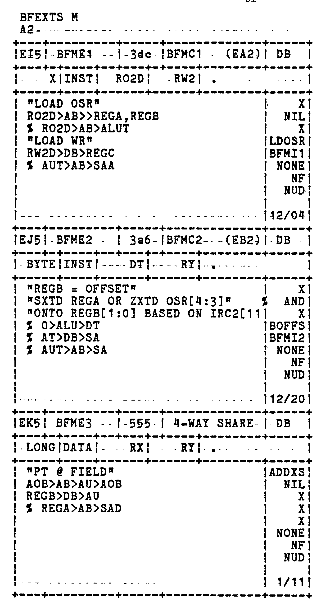
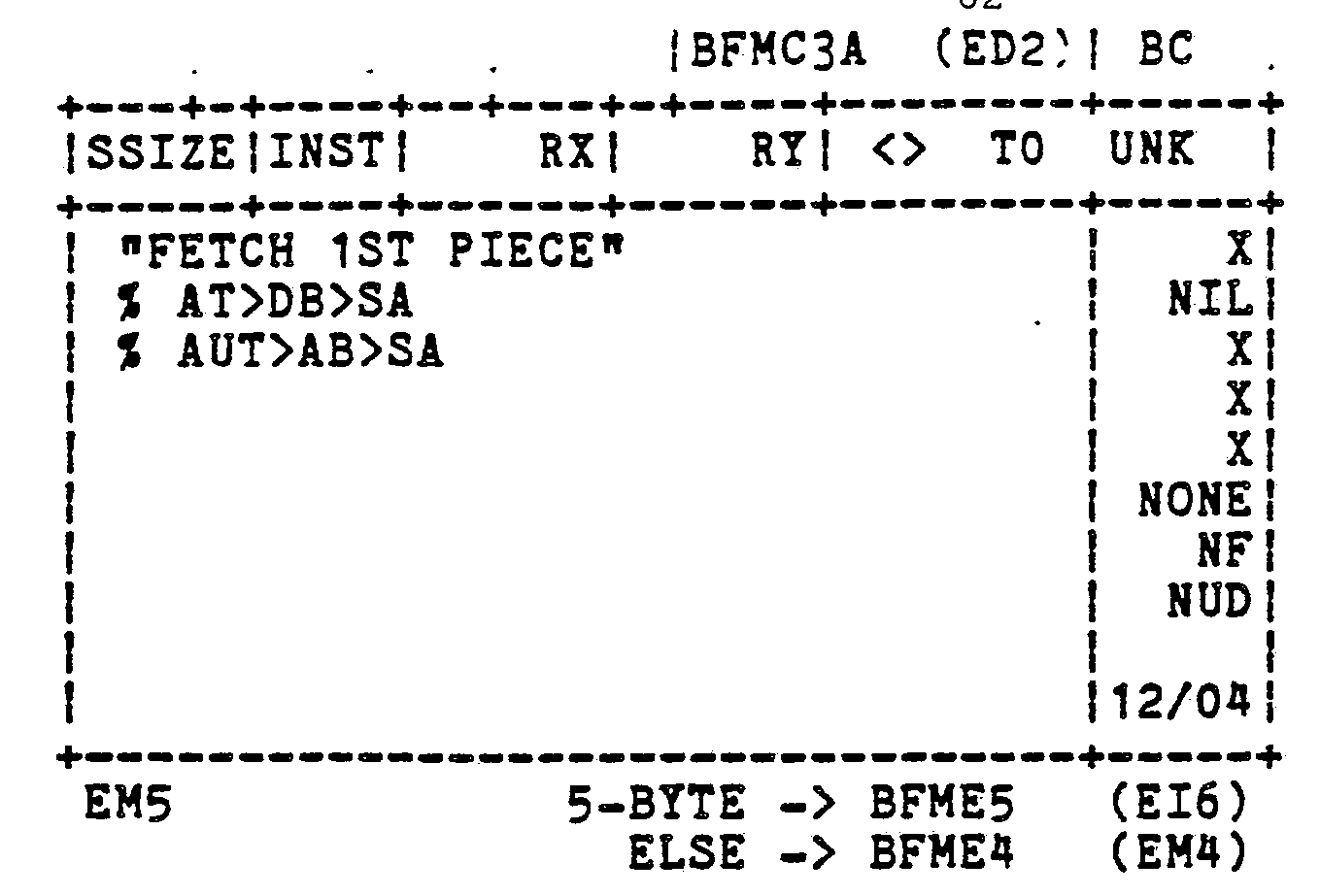


Claims
1. In a data processor adapted to perform operations upon operands having a predetermined size, including a selected operation upon a bit field having up to said predetermined size, the improvement comprising: first means for detecting that said bit field comprises portions of a pair of said operands; and second means for accessing said bit field within said pair of operands in support of said selected operations.
2. In a data processor having a bus of a predetermined width onto which a predetermined maximum number of bytes can be placed, said bus for carrying operands to support operations performed by the data processor, said data processor accessing memory on byte boundaries wherein an access is limited to the maximum number of bytes which can be placed on the bus, the improvement comprising: first means for detecting a bit field in memory which ovelaps more bytes than the predetermined number of bytes which can be placed on said bus, said bit field having a width no greater than the bus size; and second means for providing said bit field on said bus as an operand.
3. The data processor of claim 2 wherein the second means provides said bit field on said bus by: accessing a first portion of memory which contains a first portion of the bit field; rotating the first portion of the bit field a selected amount; loading said rotated first portion into a register coupled to said bus; accessing a second portion of memory which contains the remaining portion of the bit field; rotating the remaining portion of the bit field a selected amount; and
inserting said rotated remaining portion of the bit field into the register; whereby the bit field can be coupled to the bus.
4. In a data processor having a bus of a predetermined width onto which a predetermined maximum number of bytes can be placed, said bus for carrying operands to support operations performed by the data processor, said data processor accessing memory on byte boundaries wherein an access is limited to the maximum number of bytes which can be placed on the bus, the improvement comprising: first means for detecting a bit field space in memory which overlaps more bytes than the predetermined number of bytes which can be placed on said bus, said bit field having a width no greater than the bus size; and second means for inserting an operand into said bit field space.
5. The data processor of claim 5 wherein the second means inserts the operand into the bit field space by: loading a first portion of memory which contains a first portion of the bit field space into a register; rotating the operand a first selected amount; inserting selected portions of the operand rotated the first selected amount into the register; and loading the contents of the register into the first portion of memory after said insertion of the selected portions of the operand rotated the first selected amount; loading a second portion of memory which contains the remaining portion of the bit field space into the register; rotating the operand a second selected amount; inserting selected portions of the operand rotated the second selected amount into the register; and
loading the contents of the register into the second portion of memory after said insertion of the selected portions of the operand rotated the second selected amount; whereby said operand is loaded into the bit field space.
6. In a data processor having a bus of a predetermined width for carrying operands to support operations performed by the data processor, a method for inserting an operand into a bit field space in memory, comprising the steps of: loading a first portion of memory which contains a first portion of the bit field space into a register; rotating the operand a first selected amount; inserting selected portions of the operand rotated the first selected amount into the register; loading the contents of the register into the first portion of memory after said insertion of the selected portions of the operand rotated the first selected amount; loading a second portion of memory which contains the remaining portion of the bit field space into the register; rotating the operand a second selected amount; inserting selected portions of the operand rotated the second selected amount into the register; and loading the contents of the register into the second portion of memory after said insertion of the selected portions of the operand rotated the second selected amount; whereby said operand is loaded into the bit field space.
7. In a data processor having a bus of a predetermined width for carrying operands to support operations performed by the data processor, a method for providing the data processor access to a bit field, comprising the steps of: accessing a first portion of memory which contains a first portion of the bit field;
rotating the first portion of the bit field a selected amount; loading said rotated first portion into a register coupled to said bus; accessing a second portion of memory which contains the remaining portion of the bit field; rotating the remaining portion of the bit field a selected amount; and inserting the said rotated remaining portion of the bit field into the register; whereby the bit field can be coupled to the bus.
Priority Applications (1)
| Application Number | Priority Date | Filing Date | Title |
|---|---|---|---|
| KR1019860700118A KR860700163A (en) | 1984-06-27 | 1986-02-26 | Bitfield command method and device |
Applications Claiming Priority (2)
| Application Number | Priority Date | Filing Date | Title |
|---|---|---|---|
| US62506384A | 1984-06-27 | 1984-06-27 | |
| US625,063 | 1984-06-27 |
Publications (1)
| Publication Number | Publication Date |
|---|---|
| WO1986000433A1 true WO1986000433A1 (en) | 1986-01-16 |
Family
ID=24504422
Family Applications (1)
| Application Number | Title | Priority Date | Filing Date |
|---|---|---|---|
| PCT/US1985/000719 WO1986000433A1 (en) | 1984-06-27 | 1985-04-22 | Method and apparatus for a bit field instruction |
Country Status (4)
| Country | Link |
|---|---|
| EP (1) | EP0187762A4 (en) |
| JP (1) | JPS61502566A (en) |
| KR (1) | KR860700163A (en) |
| WO (1) | WO1986000433A1 (en) |
Cited By (1)
| Publication number | Priority date | Publication date | Assignee | Title |
|---|---|---|---|---|
| EP0465322A2 (en) * | 1990-06-29 | 1992-01-08 | Digital Equipment Corporation | In-register data manipulation in reduced instruction set processor |
Citations (6)
| Publication number | Priority date | Publication date | Assignee | Title |
|---|---|---|---|---|
| US3916388A (en) * | 1974-05-30 | 1975-10-28 | Ibm | Shifting apparatus for automatic data alignment |
| US4103329A (en) * | 1976-12-28 | 1978-07-25 | International Business Machines Corporation | Data processing system with improved bit field handling |
| US4135242A (en) * | 1977-11-07 | 1979-01-16 | Ncr Corporation | Method and processor having bit-addressable scratch pad memory |
| US4189772A (en) * | 1978-03-16 | 1980-02-19 | International Business Machines Corporation | Operand alignment controls for VFL instructions |
| US4219874A (en) * | 1978-03-17 | 1980-08-26 | Gusev Valery | Data processing device for variable length multibyte data fields |
| US4520439A (en) * | 1981-01-05 | 1985-05-28 | Sperry Corporation | Variable field partial write data merge |
Family Cites Families (2)
| Publication number | Priority date | Publication date | Assignee | Title |
|---|---|---|---|---|
| DE3138897A1 (en) * | 1981-09-30 | 1983-04-14 | Siemens AG, 1000 Berlin und 8000 München | CIRCUIT FOR THE PROCESSING OF STORAGE OPERANDS FOR DECIMAL AND LOGICAL COMMANDS |
| US4500958A (en) * | 1982-04-21 | 1985-02-19 | Digital Equipment Corporation | Memory controller with data rotation arrangement |
-
1985
- 1985-04-22 EP EP19850902326 patent/EP0187762A4/en not_active Withdrawn
- 1985-04-22 JP JP60501965A patent/JPS61502566A/en active Pending
- 1985-04-22 WO PCT/US1985/000719 patent/WO1986000433A1/en not_active Application Discontinuation
-
1986
- 1986-02-26 KR KR1019860700118A patent/KR860700163A/en not_active Application Discontinuation
Patent Citations (6)
| Publication number | Priority date | Publication date | Assignee | Title |
|---|---|---|---|---|
| US3916388A (en) * | 1974-05-30 | 1975-10-28 | Ibm | Shifting apparatus for automatic data alignment |
| US4103329A (en) * | 1976-12-28 | 1978-07-25 | International Business Machines Corporation | Data processing system with improved bit field handling |
| US4135242A (en) * | 1977-11-07 | 1979-01-16 | Ncr Corporation | Method and processor having bit-addressable scratch pad memory |
| US4189772A (en) * | 1978-03-16 | 1980-02-19 | International Business Machines Corporation | Operand alignment controls for VFL instructions |
| US4219874A (en) * | 1978-03-17 | 1980-08-26 | Gusev Valery | Data processing device for variable length multibyte data fields |
| US4520439A (en) * | 1981-01-05 | 1985-05-28 | Sperry Corporation | Variable field partial write data merge |
Non-Patent Citations (1)
| Title |
|---|
| See also references of EP0187762A4 * |
Cited By (3)
| Publication number | Priority date | Publication date | Assignee | Title |
|---|---|---|---|---|
| EP0465322A2 (en) * | 1990-06-29 | 1992-01-08 | Digital Equipment Corporation | In-register data manipulation in reduced instruction set processor |
| EP0465322A3 (en) * | 1990-06-29 | 1992-11-19 | Digital Equipment Corporation | In-register data manipulation in reduced instruction set processor |
| US5367705A (en) * | 1990-06-29 | 1994-11-22 | Digital Equipment Corp. | In-register data manipulation using data shift in reduced instruction set processor |
Also Published As
| Publication number | Publication date |
|---|---|
| JPS61502566A (en) | 1986-11-06 |
| EP0187762A4 (en) | 1987-10-19 |
| EP0187762A1 (en) | 1986-07-23 |
| KR860700163A (en) | 1986-03-31 |
Similar Documents
| Publication | Publication Date | Title |
|---|---|---|
| WO1986000434A1 (en) | Method and apparatus for a compare and swap instruction | |
| JP2796590B2 (en) | Memory device and data processing device using the same | |
| EP0375950B1 (en) | Method and hardware implementation of complex data transfer instructions | |
| JP2539199B2 (en) | Digital processor controller | |
| US4591972A (en) | Data processing system with unique microcode control | |
| AU632559B2 (en) | Control of multiple function units with parallel operation in a microcoded execution unit | |
| US4569018A (en) | Digital data processing system having dual-purpose scratchpad and address translation memory | |
| US5347636A (en) | Data processor which efficiently accesses main memory and input/output devices | |
| JPH05173837A (en) | Data processing system wherein static masking and dynamic masking of information in operand are both provided | |
| US4584666A (en) | Method and apparatus for signed and unsigned bounds check | |
| US4597041A (en) | Method and apparatus for enhancing the operation of a data processing system | |
| JPS61114353A (en) | Access collation structural body for digital data processingsystem having demand time paging memory | |
| WO1981000631A1 (en) | Microcomputer arranged for direct memory access | |
| US5179671A (en) | Apparatus for generating first and second selection signals for aligning words of an operand and bytes within these words respectively | |
| AU628458B2 (en) | Apparatus and method for address translation of non-aligned double word virtual addresses | |
| WO1986000433A1 (en) | Method and apparatus for a bit field instruction | |
| US6108761A (en) | Method of and apparatus for saving time performing certain transfer instructions | |
| US4737908A (en) | Buffer memory control system | |
| EP0177712B1 (en) | Masked data fetch and modifying device | |
| EP0110613B1 (en) | Digital data processing system | |
| EP0312183A2 (en) | Digital data processing system | |
| EP0229253A2 (en) | Data processor with virtual memory management | |
| EP0149858A2 (en) | Data processing system | |
| WO1986000435A1 (en) | Three word instruction pipeline | |
| CA1204216A (en) | Digital data processing system with vertical and horizontal microcode control |
Legal Events
| Date | Code | Title | Description |
|---|---|---|---|
| AK | Designated states |
Designated state(s): JP KR |
|
| AL | Designated countries for regional patents |
Designated state(s): DE FR GB IT NL |
|
| WWE | Wipo information: entry into national phase |
Ref document number: 1985902326 Country of ref document: EP |
|
| WWP | Wipo information: published in national office |
Ref document number: 1985902326 Country of ref document: EP |
|
| WWW | Wipo information: withdrawn in national office |
Ref document number: 1985902326 Country of ref document: EP |