US9966356B2 - Laser-induced forming and transfer of shaped metallic interconnects - Google Patents
Laser-induced forming and transfer of shaped metallic interconnects Download PDFInfo
- Publication number
- US9966356B2 US9966356B2 US15/489,958 US201715489958A US9966356B2 US 9966356 B2 US9966356 B2 US 9966356B2 US 201715489958 A US201715489958 A US 201715489958A US 9966356 B2 US9966356 B2 US 9966356B2
- Authority
- US
- United States
- Prior art keywords
- laser
- interconnects
- metallic interconnects
- shaped metallic
- forming
- Prior art date
- Legal status (The legal status is an assumption and is not a legal conclusion. Google has not performed a legal analysis and makes no representation as to the accuracy of the status listed.)
- Active
Links
Images


Classifications
-
- H01L24/48—
-
- H—ELECTRICITY
- H10—SEMICONDUCTOR DEVICES; ELECTRIC SOLID-STATE DEVICES NOT OTHERWISE PROVIDED FOR
- H10W—GENERIC PACKAGES, INTERCONNECTIONS, CONNECTORS OR OTHER CONSTRUCTIONAL DETAILS OF DEVICES COVERED BY CLASS H10
- H10W70/00—Package substrates; Interposers; Redistribution layers [RDL]
- H10W70/01—Manufacture or treatment
- H10W70/04—Manufacture or treatment of leadframes
- H10W70/042—Etching
-
- H—ELECTRICITY
- H10—SEMICONDUCTOR DEVICES; ELECTRIC SOLID-STATE DEVICES NOT OTHERWISE PROVIDED FOR
- H10W—GENERIC PACKAGES, INTERCONNECTIONS, CONNECTORS OR OTHER CONSTRUCTIONAL DETAILS OF DEVICES COVERED BY CLASS H10
- H10W72/00—Interconnections or connectors in packages
- H10W72/071—Connecting or disconnecting
- H10W72/075—Connecting or disconnecting of bond wires
-
- H01L21/4828—
-
- H01L21/76885—
-
- H01L24/05—
-
- H01L24/43—
-
- H01L24/85—
-
- H—ELECTRICITY
- H10—SEMICONDUCTOR DEVICES; ELECTRIC SOLID-STATE DEVICES NOT OTHERWISE PROVIDED FOR
- H10W—GENERIC PACKAGES, INTERCONNECTIONS, CONNECTORS OR OTHER CONSTRUCTIONAL DETAILS OF DEVICES COVERED BY CLASS H10
- H10W20/00—Interconnections in chips, wafers or substrates
- H10W20/01—Manufacture or treatment
- H10W20/031—Manufacture or treatment of conductive parts of the interconnections
- H10W20/063—Manufacture or treatment of conductive parts of the interconnections by forming conductive members before forming protective insulating material
-
- H—ELECTRICITY
- H10—SEMICONDUCTOR DEVICES; ELECTRIC SOLID-STATE DEVICES NOT OTHERWISE PROVIDED FOR
- H10W—GENERIC PACKAGES, INTERCONNECTIONS, CONNECTORS OR OTHER CONSTRUCTIONAL DETAILS OF DEVICES COVERED BY CLASS H10
- H10W72/00—Interconnections or connectors in packages
- H10W72/90—Bond pads, in general
-
- H—ELECTRICITY
- H01—ELECTRIC ELEMENTS
- H01G—CAPACITORS; CAPACITORS, RECTIFIERS, DETECTORS, SWITCHING DEVICES, LIGHT-SENSITIVE OR TEMPERATURE-SENSITIVE DEVICES OF THE ELECTROLYTIC TYPE
- H01G4/00—Fixed capacitors; Processes of their manufacture
- H01G4/38—Multiple capacitors, i.e. structural combinations of fixed capacitors
-
- H01L2224/04042—
-
- H01L2224/29147—
-
- H01L2224/435—
-
- H01L2224/45014—
-
- H01L2224/4805—
-
- H01L2224/48101—
-
- H01L2224/4814—
-
- H01L2224/48472—
-
- H01L2224/8585—
-
- H—ELECTRICITY
- H10—SEMICONDUCTOR DEVICES; ELECTRIC SOLID-STATE DEVICES NOT OTHERWISE PROVIDED FOR
- H10W—GENERIC PACKAGES, INTERCONNECTIONS, CONNECTORS OR OTHER CONSTRUCTIONAL DETAILS OF DEVICES COVERED BY CLASS H10
- H10W72/00—Interconnections or connectors in packages
- H10W72/01—Manufacture or treatment
- H10W72/015—Manufacture or treatment of bond wires
- H10W72/01504—Manufacture or treatment of bond wires using temporary auxiliary members, e.g. using sacrificial coatings or handle substrates
-
- H—ELECTRICITY
- H10—SEMICONDUCTOR DEVICES; ELECTRIC SOLID-STATE DEVICES NOT OTHERWISE PROVIDED FOR
- H10W—GENERIC PACKAGES, INTERCONNECTIONS, CONNECTORS OR OTHER CONSTRUCTIONAL DETAILS OF DEVICES COVERED BY CLASS H10
- H10W72/00—Interconnections or connectors in packages
- H10W72/01—Manufacture or treatment
- H10W72/015—Manufacture or treatment of bond wires
- H10W72/01551—Changing the shapes of bond wires
-
- H—ELECTRICITY
- H10—SEMICONDUCTOR DEVICES; ELECTRIC SOLID-STATE DEVICES NOT OTHERWISE PROVIDED FOR
- H10W—GENERIC PACKAGES, INTERCONNECTIONS, CONNECTORS OR OTHER CONSTRUCTIONAL DETAILS OF DEVICES COVERED BY CLASS H10
- H10W72/00—Interconnections or connectors in packages
- H10W72/01—Manufacture or treatment
- H10W72/015—Manufacture or treatment of bond wires
- H10W72/01561—Chemical or physical modification, e.g. by sintering or anodisation
-
- H—ELECTRICITY
- H10—SEMICONDUCTOR DEVICES; ELECTRIC SOLID-STATE DEVICES NOT OTHERWISE PROVIDED FOR
- H10W—GENERIC PACKAGES, INTERCONNECTIONS, CONNECTORS OR OTHER CONSTRUCTIONAL DETAILS OF DEVICES COVERED BY CLASS H10
- H10W72/00—Interconnections or connectors in packages
- H10W72/01—Manufacture or treatment
- H10W72/016—Manufacture or treatment of strap connectors
- H10W72/01651—Changing the shapes of strap connectors
-
- H—ELECTRICITY
- H10—SEMICONDUCTOR DEVICES; ELECTRIC SOLID-STATE DEVICES NOT OTHERWISE PROVIDED FOR
- H10W—GENERIC PACKAGES, INTERCONNECTIONS, CONNECTORS OR OTHER CONSTRUCTIONAL DETAILS OF DEVICES COVERED BY CLASS H10
- H10W72/00—Interconnections or connectors in packages
- H10W72/071—Connecting or disconnecting
- H10W72/075—Connecting or disconnecting of bond wires
- H10W72/07502—Connecting or disconnecting of bond wires using an auxiliary member
- H10W72/07504—Connecting or disconnecting of bond wires using an auxiliary member the auxiliary member being temporary, e.g. a sacrificial coating
- H10W72/07507—Connecting or disconnecting of bond wires using an auxiliary member the auxiliary member being temporary, e.g. a sacrificial coating the auxiliary member being a temporary substrate, e.g. a removable substrate
-
- H—ELECTRICITY
- H10—SEMICONDUCTOR DEVICES; ELECTRIC SOLID-STATE DEVICES NOT OTHERWISE PROVIDED FOR
- H10W—GENERIC PACKAGES, INTERCONNECTIONS, CONNECTORS OR OTHER CONSTRUCTIONAL DETAILS OF DEVICES COVERED BY CLASS H10
- H10W72/00—Interconnections or connectors in packages
- H10W72/071—Connecting or disconnecting
- H10W72/075—Connecting or disconnecting of bond wires
- H10W72/07511—Treating the bonding area before connecting, e.g. by applying flux or cleaning
-
- H—ELECTRICITY
- H10—SEMICONDUCTOR DEVICES; ELECTRIC SOLID-STATE DEVICES NOT OTHERWISE PROVIDED FOR
- H10W—GENERIC PACKAGES, INTERCONNECTIONS, CONNECTORS OR OTHER CONSTRUCTIONAL DETAILS OF DEVICES COVERED BY CLASS H10
- H10W72/00—Interconnections or connectors in packages
- H10W72/071—Connecting or disconnecting
- H10W72/075—Connecting or disconnecting of bond wires
- H10W72/07531—Techniques
- H10W72/07537—Techniques using a polymer adhesive, e.g. an adhesive based on silicone or epoxy
-
- H—ELECTRICITY
- H10—SEMICONDUCTOR DEVICES; ELECTRIC SOLID-STATE DEVICES NOT OTHERWISE PROVIDED FOR
- H10W—GENERIC PACKAGES, INTERCONNECTIONS, CONNECTORS OR OTHER CONSTRUCTIONAL DETAILS OF DEVICES COVERED BY CLASS H10
- H10W72/00—Interconnections or connectors in packages
- H10W72/071—Connecting or disconnecting
- H10W72/075—Connecting or disconnecting of bond wires
- H10W72/07551—Connecting or disconnecting of bond wires characterised by changes in properties of the bond wires during the connecting
- H10W72/07553—Connecting or disconnecting of bond wires characterised by changes in properties of the bond wires during the connecting changes in shapes
-
- H—ELECTRICITY
- H10—SEMICONDUCTOR DEVICES; ELECTRIC SOLID-STATE DEVICES NOT OTHERWISE PROVIDED FOR
- H10W—GENERIC PACKAGES, INTERCONNECTIONS, CONNECTORS OR OTHER CONSTRUCTIONAL DETAILS OF DEVICES COVERED BY CLASS H10
- H10W72/00—Interconnections or connectors in packages
- H10W72/071—Connecting or disconnecting
- H10W72/075—Connecting or disconnecting of bond wires
- H10W72/07551—Connecting or disconnecting of bond wires characterised by changes in properties of the bond wires during the connecting
- H10W72/07554—Connecting or disconnecting of bond wires characterised by changes in properties of the bond wires during the connecting changes in dispositions
-
- H—ELECTRICITY
- H10—SEMICONDUCTOR DEVICES; ELECTRIC SOLID-STATE DEVICES NOT OTHERWISE PROVIDED FOR
- H10W—GENERIC PACKAGES, INTERCONNECTIONS, CONNECTORS OR OTHER CONSTRUCTIONAL DETAILS OF DEVICES COVERED BY CLASS H10
- H10W72/00—Interconnections or connectors in packages
- H10W72/071—Connecting or disconnecting
- H10W72/076—Connecting or disconnecting of strap connectors
- H10W72/07602—Connecting or disconnecting of strap connectors using an auxiliary member
- H10W72/07604—Connecting or disconnecting of strap connectors using an auxiliary member the auxiliary member being temporary, e.g. a sacrificial coating
- H10W72/07607—Connecting or disconnecting of strap connectors using an auxiliary member the auxiliary member being temporary, e.g. a sacrificial coating the auxiliary member being a temporary substrate, e.g. a removable substrate
-
- H—ELECTRICITY
- H10—SEMICONDUCTOR DEVICES; ELECTRIC SOLID-STATE DEVICES NOT OTHERWISE PROVIDED FOR
- H10W—GENERIC PACKAGES, INTERCONNECTIONS, CONNECTORS OR OTHER CONSTRUCTIONAL DETAILS OF DEVICES COVERED BY CLASS H10
- H10W72/00—Interconnections or connectors in packages
- H10W72/071—Connecting or disconnecting
- H10W72/076—Connecting or disconnecting of strap connectors
- H10W72/07611—Treating the bonding area before connecting, e.g. by applying flux or cleaning
-
- H—ELECTRICITY
- H10—SEMICONDUCTOR DEVICES; ELECTRIC SOLID-STATE DEVICES NOT OTHERWISE PROVIDED FOR
- H10W—GENERIC PACKAGES, INTERCONNECTIONS, CONNECTORS OR OTHER CONSTRUCTIONAL DETAILS OF DEVICES COVERED BY CLASS H10
- H10W72/00—Interconnections or connectors in packages
- H10W72/071—Connecting or disconnecting
- H10W72/076—Connecting or disconnecting of strap connectors
- H10W72/07631—Techniques
- H10W72/07637—Techniques using a polymer adhesive, e.g. an adhesive based on silicone or epoxy
-
- H—ELECTRICITY
- H10—SEMICONDUCTOR DEVICES; ELECTRIC SOLID-STATE DEVICES NOT OTHERWISE PROVIDED FOR
- H10W—GENERIC PACKAGES, INTERCONNECTIONS, CONNECTORS OR OTHER CONSTRUCTIONAL DETAILS OF DEVICES COVERED BY CLASS H10
- H10W72/00—Interconnections or connectors in packages
- H10W72/30—Die-attach connectors
- H10W72/351—Materials of die-attach connectors
- H10W72/352—Materials of die-attach connectors comprising metals or metalloids, e.g. solders
-
- H—ELECTRICITY
- H10—SEMICONDUCTOR DEVICES; ELECTRIC SOLID-STATE DEVICES NOT OTHERWISE PROVIDED FOR
- H10W—GENERIC PACKAGES, INTERCONNECTIONS, CONNECTORS OR OTHER CONSTRUCTIONAL DETAILS OF DEVICES COVERED BY CLASS H10
- H10W72/00—Interconnections or connectors in packages
- H10W72/50—Bond wires
- H10W72/531—Shapes of wire connectors
- H10W72/533—Cross-sectional shape
- H10W72/534—Cross-sectional shape being rectangular
-
- H—ELECTRICITY
- H10—SEMICONDUCTOR DEVICES; ELECTRIC SOLID-STATE DEVICES NOT OTHERWISE PROVIDED FOR
- H10W—GENERIC PACKAGES, INTERCONNECTIONS, CONNECTORS OR OTHER CONSTRUCTIONAL DETAILS OF DEVICES COVERED BY CLASS H10
- H10W72/00—Interconnections or connectors in packages
- H10W72/50—Bond wires
- H10W72/531—Shapes of wire connectors
- H10W72/5363—Shapes of wire connectors the connected ends being wedge-shaped
-
- H—ELECTRICITY
- H10—SEMICONDUCTOR DEVICES; ELECTRIC SOLID-STATE DEVICES NOT OTHERWISE PROVIDED FOR
- H10W—GENERIC PACKAGES, INTERCONNECTIONS, CONNECTORS OR OTHER CONSTRUCTIONAL DETAILS OF DEVICES COVERED BY CLASS H10
- H10W72/00—Interconnections or connectors in packages
- H10W72/50—Bond wires
- H10W72/541—Dispositions of bond wires
- H10W72/5434—Dispositions of bond wires the connected ends being on auxiliary connecting means on bond pads, e.g. on other bond wires
-
- H—ELECTRICITY
- H10—SEMICONDUCTOR DEVICES; ELECTRIC SOLID-STATE DEVICES NOT OTHERWISE PROVIDED FOR
- H10W—GENERIC PACKAGES, INTERCONNECTIONS, CONNECTORS OR OTHER CONSTRUCTIONAL DETAILS OF DEVICES COVERED BY CLASS H10
- H10W72/00—Interconnections or connectors in packages
- H10W72/50—Bond wires
- H10W72/551—Materials of bond wires
- H10W72/552—Materials of bond wires comprising metals or metalloids, e.g. silver
- H10W72/5525—Materials of bond wires comprising metals or metalloids, e.g. silver comprising copper [Cu]
-
- H—ELECTRICITY
- H10—SEMICONDUCTOR DEVICES; ELECTRIC SOLID-STATE DEVICES NOT OTHERWISE PROVIDED FOR
- H10W—GENERIC PACKAGES, INTERCONNECTIONS, CONNECTORS OR OTHER CONSTRUCTIONAL DETAILS OF DEVICES COVERED BY CLASS H10
- H10W72/00—Interconnections or connectors in packages
- H10W72/50—Bond wires
- H10W72/59—Bond pads specially adapted therefor
-
- H—ELECTRICITY
- H10—SEMICONDUCTOR DEVICES; ELECTRIC SOLID-STATE DEVICES NOT OTHERWISE PROVIDED FOR
- H10W—GENERIC PACKAGES, INTERCONNECTIONS, CONNECTORS OR OTHER CONSTRUCTIONAL DETAILS OF DEVICES COVERED BY CLASS H10
- H10W72/00—Interconnections or connectors in packages
- H10W72/60—Strap connectors, e.g. thick copper clips for grounding of power devices
- H10W72/631—Shapes of strap connectors
- H10W72/634—Cross-sectional shape
-
- H—ELECTRICITY
- H10—SEMICONDUCTOR DEVICES; ELECTRIC SOLID-STATE DEVICES NOT OTHERWISE PROVIDED FOR
- H10W—GENERIC PACKAGES, INTERCONNECTIONS, CONNECTORS OR OTHER CONSTRUCTIONAL DETAILS OF DEVICES COVERED BY CLASS H10
- H10W72/00—Interconnections or connectors in packages
- H10W72/60—Strap connectors, e.g. thick copper clips for grounding of power devices
- H10W72/641—Dispositions of strap connectors
- H10W72/646—Dispositions of strap connectors the connected ends being on auxiliary connecting means on bond pads, e.g. on a bump connector
-
- H—ELECTRICITY
- H10—SEMICONDUCTOR DEVICES; ELECTRIC SOLID-STATE DEVICES NOT OTHERWISE PROVIDED FOR
- H10W—GENERIC PACKAGES, INTERCONNECTIONS, CONNECTORS OR OTHER CONSTRUCTIONAL DETAILS OF DEVICES COVERED BY CLASS H10
- H10W72/00—Interconnections or connectors in packages
- H10W72/60—Strap connectors, e.g. thick copper clips for grounding of power devices
- H10W72/651—Materials of strap connectors
- H10W72/652—Materials of strap connectors comprising metals or metalloids, e.g. silver
-
- H—ELECTRICITY
- H10—SEMICONDUCTOR DEVICES; ELECTRIC SOLID-STATE DEVICES NOT OTHERWISE PROVIDED FOR
- H10W—GENERIC PACKAGES, INTERCONNECTIONS, CONNECTORS OR OTHER CONSTRUCTIONAL DETAILS OF DEVICES COVERED BY CLASS H10
- H10W90/00—Package configurations
- H10W90/701—Package configurations characterised by the relative positions of pads or connectors relative to package parts
- H10W90/751—Package configurations characterised by the relative positions of pads or connectors relative to package parts of bond wires
- H10W90/753—Package configurations characterised by the relative positions of pads or connectors relative to package parts of bond wires between laterally-adjacent chips
Definitions
- Conformal circuits are needed to place electronics in three-dimensional (3D) configurations rather than standard planar or 2D, a requirement that is becoming more urgent as 3D printed electronics mature and become more reliable.
- Flexible circuits require the integration of components into substrates or packages that are mechanically compliant so that they can conform, bend, stretch or fold to a level pre-designed without causing the circuit to fail.
- hybrid circuits are comprised of distinct discrete components integrated into single or multilayer architectures assembled on non-traditional substrates as opposed to printed circuit boards. Examples of such components include logic, communication, memory, sensing and power elements all integrated into a functional system or module.
- the overarching challenge is to move away from traditional printed circuit fabrication techniques, which limit the ability to produce conformal, flexible and hybrid designs.
- One of the most difficult obstacles toward this goal is to replace the way the interconnects on a circuit are currently generated using soldering of packaged components, which are bulky and of limited use in a conformal and/or flexible design, and wire-bonding of unpackaged devices (incompatible with the low profile requirements of most conformal and hybrid designs).
- Processing techniques such as laser direct-write (LDW) offer a viable alternative for the fabrication of low profile yet compliant, and robust, yet electrically conductive interconnects.
- LDW laser direct-write
- These techniques allow the patterning of customizable electrically conductive metallic beams, which can be shaped or formed via laser folding to accommodate misalignment and strains between components.
- the same techniques then enable the non-contact laser-transfer of these shaped beams placing them precisely across the devices to electrically connect them across a gap.
- the ability to shape and print low profile, electrically conductive and free-standing interconnects across a gap for wiring the components required for the fabrication of conformal, flexible and hybrid electronics becomes possible for the first time through the application of this invention.
- this invention extends our previous work on the laser-induced forward transfer (LIFT) of discrete devices to include the transfer of metallic interconnects and commercial solder pastes.
- LIFT laser-induced forward transfer
- this invention incorporates the laser-induced bending and/or shaping of these interconnects in order to create structures that are capable of accommodating very large strains.
- a LIFT process is also used to print conductive adhesives or solder pastes, resulting in low-profile interconnects that are both mechanically and electrically attached to the device and surrounding circuit and are capable of withstanding deformation and strains that would result in the failure of a traditionally inkjet printed metallic trace.
- This invention allows for the implementation of reliable low-profile interconnects able to conduct high current loads (>1 Amp) for printed electronic applications.
- This invention utilizes laser forming or shaping of electrically conductive metal beams, followed by laser transfer of these beams over the device pads to form robust, free-standing interconnects between discrete devices or components.
- the methods disclosed in this invention can be used to generate all kinds of electrical interconnects between discrete devices and other components such as chip carriers, flexible substrates and external connectors found in all types of electronic circuit and systems.
- This invention is related to traditional wire bonding, however, significant advantages are taught herein that result in laser-shaped and transferred interconnects occupying a fraction of the volume due to their low profile, as shown schematically in FIG. 1 .
- This invention solves long-standing problems and allows for embedded and flexible electronic circuits and systems.
- FIG. 1 is a schematic diagram showing the typical profiles of (a) wire-bonded interconnects vs. (b) laser transferred shaped interconnects.
- FIG. 2 is a schematic diagram illustrating the process required for the laser transfer of flat interconnects. The limitations of this configuration when subjected to strain are shown in (d). a) shows the donor substrate with patterned flat copper beams. b) shows flat copper beams during laser-transfer. c) shows typical dimensions of transferred copper interconnects. d) shows interconnect fails due to strain from thermal expansion.
- FIG. 3 is a schematic illustrating the process required for the laser forming/shaping and subsequent laser transfer to form electrically conductive and mechanically compliant interconnects.
- a) shows the donor substrate with flat copper beam.
- b) shows the donor substrate with flat copper beam and stencil.
- c) shows copper beam during laser-shaping.
- d) shows shaped copper beam during laser-transfer.
- e) shows typical dimensions of shaped transferred copper interconnects.
- f) shows interconnects stretch without failing under strain from thermal expansion.
- FIG. 4 illustrates the steps for the preparation of the donor substrate comprising: (a) Quartz disc (5 cm dia), (b) coated with a wax release layer, (c) onto which a 12.5 ⁇ m thick copper foil is attached and then (d) laser patterned into an array of beams.
- FIG. 5 illustrates a patterned donor substrate showing array of copper beams (a) before and (b) after laser patterning. Higher magnification images of the laser-shaped beams are shown in (c) and (d).
- FIG. 6 illustrates photographs showing an electrically functional circuit comprising of four silicon capacitors connected in parallel using a series of laser transferred flat beams as interconnects.
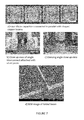
- FIG. 7 illustrates photographs showing an electrically functional circuit comprising of four silicon capacitors connected in parallel using a series of laser-shaped and then laser transferred beams as interconnects.
- This invention allows for the implementation of reliable low-profile interconnects able to conduct high current loads (>1 Amp) for printed electronic applications.
- This invention utilizes laser forming or shaping of electrically conductive metal beams, followed by laser transfer of these beams over the device pads to form robust, free-standing interconnects between discrete devices or components.
- the methods disclosed in this invention concerning laser shaping and transferring, generate all kinds of electrical interconnects between discrete devices and other components.
- Examples include chip carriers, flexible substrates and external connectors found in all types of electronic circuit and systems.
- This invention solves long-standing problems and allows for embedded and flexible electronic circuits and systems that are superior to the prior art.
- the invention herein describes a novel laser-based method for the fabrication of low-profile, free-standing, compliant and electrically conductive interconnects.
- FIG. 2 A schematic of the process is shown in FIG. 2 for the fabrication of flat interconnects and in FIG. 3 for the fabrication of shaped interconnects.
- the elements involved in the method of this invention comprise of a laser system, beam preparation and laser transfer of beams to form interconnects. Those elements are described in the following sections with example embodiments.
- a 10 watt, 355 nm, solid-state, Q-switched laser with a 30-40 nsec pulse width is used for the patterning, shaping and transfer of the metal interconnects.
- the laser pulses are delivered to the sample through a 10 ⁇ UV microscope objective or a galvanometric beam scanner with 100 mm focal length telecentric lens.
- the full Gaussian beam is used for laser shaping operations.
- the laser beam is directed through an aperture and imaged onto the sample in order to achieve “top hat” illumination over a well defined spot size. The illuminated spot size is varied by changing the aperture.
- An acousto-optic modulator is used as a fast shutter to deliver laser pulses on demand and control the delivered energy.
- Two independent translation stages allow the movement of the donor substrate with respect to the receive substrate for alignment and focusing purposes.
- An adhesion/release layer is formed on a 5 cm dia. quartz disc by dissolving a low temperature wax (Apiezon-W) in toluene and spin coating the solution at room temperature.
- a copper foil (12.5 microns thick) is laid over the wax layer and bonded using a heated press at approximately 80° C.
- Conventional photoresist is applied by spin coating and laser exposed along the desired interconnect pattern.
- This donor substrate, combined with the release layer and the patterned copper is referred to as the ribbon.
- the patterned copper interconnects can be transferred directly or laser-bent and subsequently transferred onto a receiving substrate. Bending of the copper beams is achieved by placing a thin metal stencil (400 micron steel) over the ribbon and firing the laser through the glass slide, into the open regions of the stencil. The laser pulse pushes the copper beam away from the ribbon by as much as several hundred microns. In the regions covered by the stencil, the copper beam is confined to the surface of the ribbon. The copper beam is thereby plastically deformed into a shape defined by the stencil and the laser pulse.
- the measured lase fluence during the bending of the copper beams is around 1.1 J/cm 2 for 12.5 ⁇ m thick beams.
- FIG. 3 The laser initiated bending of the copper beams is shown schematically in FIG. 3 .
- FIG. 4 shows photographs illustrating the steps in the preparation of the donor substrate and the resulting array of copper beams after laser patterning. Images showing the beams on the donor substrate before and after laser-shaping can be seen in FIG. 5 .
- a conductive epoxy is used to attach the copper beam to the device.
- Initial results were achieved by manually placing small quantities of the conductive epoxy H20E on the device pads with a hypodermic needle.
- H20E is a two-part silver-filed epoxy with relatively long curing time ( ⁇ 2.5 days).
- Subsequent results used a LIFT process to laser transfer the conductive epoxy in the form of voxels ⁇ 10 ⁇ m thick onto the device or onto the copper beam.
- the ribbon was positioned approximately 10-30 ⁇ m above the receiving device. The laser was then fired with an appropriate energy and spot size so as to release the copper in a controlled fashion.
- the laser transferred flat interconnects work relatively well except when the circuit is mechanically strained, for example due to expansion or contraction during heating or cooling, as shown schematically in FIG. 2( d ) .
- Examples of interconnected devices in this case individual silicon capacitors mounted on a flat substrate are shown with flat interconnects ( FIG. 6 ) and with laser-shaped interconnects ( FIG. 7 ).
- the circuits are electrically functional, i.e. the capacitors connected in parallel for these examples exhibited the expected value for their total capacitance.
- the measured capacitance of the individual devices was 3.27 ⁇ F, and the calculated capacitance of four of them connected in parallel was expected to be 13.08 ⁇ F.
- the overarching challenge is to move away from traditional printed circuit fabrication techniques, which limit the ability to produce conformal, flexible and hybrid designs.
- One of the most difficult obstacles toward this goal is to replace the way the interconnects on a circuit are currently generated using soldering of packaged components (bulky and of limited use in a conformal and/or flexible design) and wire-bonding of unpackaged devices (incompatible with the low profile requirements of most conformal and hybrid designs).
- the solution to these problems calls for the development of processes and techniques that allow the printing of low profile, yet robust interconnects between discrete components at low temperatures.
- the low profile requirement eliminates the possibility of using wire-bonding since attachment of the wire to the pads requires that it extends high above the device surface to accommodate strains during the bonding process.
- laser-shaped and laser-transferred interconnects address all the challenges above mentioned by providing a method for the fabrication of arbitrary size and shape beams made from bulk metal and directly placed across the contacts of discrete devices to provide electrical connections that can withstand typical strains and deformations encountered during the operation of electronic circuits.
- the resulting laser-shaped and laser-transferred interconnects are fully compatible with the design requirements of next generation conformal, flexible and hybrid circuit designs.
- This invention provides a method that can be scaled to achieve high throughput rates for the fabrication and placement of shaped interconnects with customizable lengths and shapes, making it compatible with the fabrication of both circuit designs for mission specific applications requiring low production quantities as well as commercial high volume products.
- This invention allows for a smaller and more robust device.
- the approach described herein is unique and offers capabilities that cannot be realized with current processes or technologies.
Landscapes
- Engineering & Computer Science (AREA)
- Manufacturing & Machinery (AREA)
- Manufacturing Of Printed Wiring (AREA)
Abstract
Description
-
- a. Fabrication of array of isolated copper foils with the desired dimensions by laser patterning.
- b. Laser decomposition of polymer backing layer resulting in the release and transfer of one or more copper foils.
- c. Landing of the foil(s) precisely over the contact pads on the devices and curing of the conductive paste for mechanical attachment and electrical conduction.
Claims (8)
Priority Applications (2)
| Application Number | Priority Date | Filing Date | Title |
|---|---|---|---|
| US15/489,958 US9966356B2 (en) | 2015-10-08 | 2017-04-18 | Laser-induced forming and transfer of shaped metallic interconnects |
| US15/962,736 US10297565B2 (en) | 2015-10-08 | 2018-04-25 | Electronic device by laser-induced forming and transfer of shaped metallic interconnects |
Applications Claiming Priority (3)
| Application Number | Priority Date | Filing Date | Title |
|---|---|---|---|
| US201562238892P | 2015-10-08 | 2015-10-08 | |
| US15/178,930 US9685349B2 (en) | 2015-10-08 | 2016-06-10 | Laser-induced forming and transfer of shaped metallic interconnects |
| US15/489,958 US9966356B2 (en) | 2015-10-08 | 2017-04-18 | Laser-induced forming and transfer of shaped metallic interconnects |
Related Parent Applications (1)
| Application Number | Title | Priority Date | Filing Date |
|---|---|---|---|
| US15/178,930 Continuation US9685349B2 (en) | 2015-10-08 | 2016-06-10 | Laser-induced forming and transfer of shaped metallic interconnects |
Related Child Applications (1)
| Application Number | Title | Priority Date | Filing Date |
|---|---|---|---|
| US15/962,736 Continuation US10297565B2 (en) | 2015-10-08 | 2018-04-25 | Electronic device by laser-induced forming and transfer of shaped metallic interconnects |
Publications (2)
| Publication Number | Publication Date |
|---|---|
| US20170221851A1 US20170221851A1 (en) | 2017-08-03 |
| US9966356B2 true US9966356B2 (en) | 2018-05-08 |
Family
ID=58499879
Family Applications (3)
| Application Number | Title | Priority Date | Filing Date |
|---|---|---|---|
| US15/178,930 Active US9685349B2 (en) | 2015-10-08 | 2016-06-10 | Laser-induced forming and transfer of shaped metallic interconnects |
| US15/489,958 Active US9966356B2 (en) | 2015-10-08 | 2017-04-18 | Laser-induced forming and transfer of shaped metallic interconnects |
| US15/962,736 Active US10297565B2 (en) | 2015-10-08 | 2018-04-25 | Electronic device by laser-induced forming and transfer of shaped metallic interconnects |
Family Applications Before (1)
| Application Number | Title | Priority Date | Filing Date |
|---|---|---|---|
| US15/178,930 Active US9685349B2 (en) | 2015-10-08 | 2016-06-10 | Laser-induced forming and transfer of shaped metallic interconnects |
Family Applications After (1)
| Application Number | Title | Priority Date | Filing Date |
|---|---|---|---|
| US15/962,736 Active US10297565B2 (en) | 2015-10-08 | 2018-04-25 | Electronic device by laser-induced forming and transfer of shaped metallic interconnects |
Country Status (1)
| Country | Link |
|---|---|
| US (3) | US9685349B2 (en) |
Families Citing this family (3)
| Publication number | Priority date | Publication date | Assignee | Title |
|---|---|---|---|---|
| US10181449B1 (en) * | 2017-09-28 | 2019-01-15 | Taiwan Semiconductor Manufacturing Co., Ltd. | Semiconductor structure |
| CN111360106B (en) * | 2020-02-20 | 2022-02-08 | 上海航天精密机械研究所 | Flexible loading platform suitable for laser bending forming of plate |
| WO2021202741A1 (en) * | 2020-03-31 | 2021-10-07 | Rashid Mavliev | Methods and systems of forming metal interconnect layers |
Citations (3)
| Publication number | Priority date | Publication date | Assignee | Title |
|---|---|---|---|---|
| US20090075214A1 (en) * | 2007-09-13 | 2009-03-19 | Semiconductor Energy Laboratory Co., Ltd. | Manufacturing method of light emitting device, and evaporation donor substrate |
| US7919340B2 (en) * | 2008-06-04 | 2011-04-05 | Semiconductor Energy Laboratory Co., Ltd. | Method for manufacturing light-emitting device |
| US8153201B2 (en) * | 2007-10-23 | 2012-04-10 | Semiconductor Energy Laboratory Co., Ltd. | Method of manufacturing light-emitting device, and evaporation donor substrate |
-
2016
- 2016-06-10 US US15/178,930 patent/US9685349B2/en active Active
-
2017
- 2017-04-18 US US15/489,958 patent/US9966356B2/en active Active
-
2018
- 2018-04-25 US US15/962,736 patent/US10297565B2/en active Active
Patent Citations (3)
| Publication number | Priority date | Publication date | Assignee | Title |
|---|---|---|---|---|
| US20090075214A1 (en) * | 2007-09-13 | 2009-03-19 | Semiconductor Energy Laboratory Co., Ltd. | Manufacturing method of light emitting device, and evaporation donor substrate |
| US8153201B2 (en) * | 2007-10-23 | 2012-04-10 | Semiconductor Energy Laboratory Co., Ltd. | Method of manufacturing light-emitting device, and evaporation donor substrate |
| US7919340B2 (en) * | 2008-06-04 | 2011-04-05 | Semiconductor Energy Laboratory Co., Ltd. | Method for manufacturing light-emitting device |
Non-Patent Citations (1)
| Title |
|---|
| Laser Direct-Write Techniques for Printing of Complex Materials, MRS Bulletin 30.01 (2007), 23.-31. * |
Also Published As
| Publication number | Publication date |
|---|---|
| US20180240772A1 (en) | 2018-08-23 |
| US9685349B2 (en) | 2017-06-20 |
| US10297565B2 (en) | 2019-05-21 |
| US20170221851A1 (en) | 2017-08-03 |
| US20170103902A1 (en) | 2017-04-13 |
Similar Documents
| Publication | Publication Date | Title |
|---|---|---|
| US11881414B2 (en) | Method for manufacturing glass device, and glass device | |
| CN104854686B (en) | Method for bonding bare chip dies | |
| US10297565B2 (en) | Electronic device by laser-induced forming and transfer of shaped metallic interconnects | |
| CN102017142B (en) | Three-dimensionally mounted semiconductor device and manufacturing method thereof | |
| JP2022531153A5 (en) | ||
| JP2022531153A (en) | How to electrically connect the chip to the top connector using 3D printing | |
| Kim et al. | Laser printing of conformal and multi-level 3D interconnects | |
| US20150016116A1 (en) | Flexible led light bar and manufacturing method thereof | |
| US11877398B2 (en) | PCB production by laser systems | |
| US20070105395A1 (en) | Laser functionalization and patterning of thick-film inks | |
| US12238862B2 (en) | PCB production by laser systems | |
| Auyeung et al. | Laser additive manufacturing of embedded electronics | |
| US8039762B2 (en) | Printed circuit board having a buried solder bump and a circuit layer flush with an insulating layer | |
| US7358114B2 (en) | Semiconductor device substrate, semiconductor device, and manufacturing method thereof | |
| CN102904082A (en) | Connector structure and manufacturing method thereof | |
| EP2943048B1 (en) | Board integrated interconnect | |
| JP2008277757A (en) | Solder connection between semiconductor chip and substrate and its manufacture | |
| KR20110088196A (en) | Preheating device for metal core PCB and soldering method for metal core PCB | |
| Beniam et al. | Laser printing of 3D metallic interconnects | |
| Mathews et al. | Laser induced forward transfer (lift) for direct-write fabrication and assembly of microelectronics | |
| JP2003059969A (en) | How to attach components to a welded connection support that does not require additional material | |
| Charipar et al. | Low-profile interconnects via laser-induced forward transfer | |
| US6806179B1 (en) | Connection substrate, a method of manufacturing the connection substrate, a semiconductor device, and a method of manufacturing the semiconductor device | |
| US20230240022A1 (en) | Hybrid process for pcb production by lad system | |
| JPS58169996A (en) | Electrically connecting device |
Legal Events
| Date | Code | Title | Description |
|---|---|---|---|
| AS | Assignment |
Owner name: THE GOVERNMENT OF THE UNITED STATES OF AMERICA, AS Free format text: ASSIGNMENT OF ASSIGNORS INTEREST;ASSIGNORS:MATHEWS, SCOTT A;BENIAM, IYOEL;PIQUE, ALBERTO;REEL/FRAME:042068/0408 Effective date: 20160509 |
|
| STCF | Information on status: patent grant |
Free format text: PATENTED CASE |
|
| FEPP | Fee payment procedure |
Free format text: MAINTENANCE FEE REMINDER MAILED (ORIGINAL EVENT CODE: REM.); ENTITY STATUS OF PATENT OWNER: LARGE ENTITY |
|
| FEPP | Fee payment procedure |
Free format text: SURCHARGE FOR LATE PAYMENT, LARGE ENTITY (ORIGINAL EVENT CODE: M1554); ENTITY STATUS OF PATENT OWNER: LARGE ENTITY |
|
| MAFP | Maintenance fee payment |
Free format text: PAYMENT OF MAINTENANCE FEE, 4TH YEAR, LARGE ENTITY (ORIGINAL EVENT CODE: M1551); ENTITY STATUS OF PATENT OWNER: LARGE ENTITY Year of fee payment: 4 |
|
| FEPP | Fee payment procedure |
Free format text: 7.5 YR SURCHARGE - LATE PMT W/IN 6 MO, LARGE ENTITY (ORIGINAL EVENT CODE: M1555); ENTITY STATUS OF PATENT OWNER: LARGE ENTITY |
|
| MAFP | Maintenance fee payment |
Free format text: PAYMENT OF MAINTENANCE FEE, 8TH YEAR, LARGE ENTITY (ORIGINAL EVENT CODE: M1552); ENTITY STATUS OF PATENT OWNER: LARGE ENTITY Year of fee payment: 8 |