US9947407B2 - Techniques for programming of select gates in NAND memory - Google Patents
Techniques for programming of select gates in NAND memory Download PDFInfo
- Publication number
- US9947407B2 US9947407B2 US15/599,850 US201715599850A US9947407B2 US 9947407 B2 US9947407 B2 US 9947407B2 US 201715599850 A US201715599850 A US 201715599850A US 9947407 B2 US9947407 B2 US 9947407B2
- Authority
- US
- United States
- Prior art keywords
- drain select
- select transistors
- source
- coupled
- memory
- Prior art date
- Legal status (The legal status is an assumption and is not a legal conclusion. Google has not performed a legal analysis and makes no representation as to the accuracy of the status listed.)
- Active
Links
Images


Classifications
-
- G—PHYSICS
- G11—INFORMATION STORAGE
- G11C—STATIC STORES
- G11C16/00—Erasable programmable read-only memories
- G11C16/02—Erasable programmable read-only memories electrically programmable
- G11C16/04—Erasable programmable read-only memories electrically programmable using variable threshold transistors, e.g. FAMOS
- G11C16/0483—Erasable programmable read-only memories electrically programmable using variable threshold transistors, e.g. FAMOS comprising cells having several storage transistors connected in series
-
- G—PHYSICS
- G11—INFORMATION STORAGE
- G11C—STATIC STORES
- G11C11/00—Digital stores characterised by the use of particular electric or magnetic storage elements; Storage elements therefor
- G11C11/56—Digital stores characterised by the use of particular electric or magnetic storage elements; Storage elements therefor using storage elements with more than two stable states represented by steps, e.g. of voltage, current, phase, frequency
- G11C11/5621—Digital stores characterised by the use of particular electric or magnetic storage elements; Storage elements therefor using storage elements with more than two stable states represented by steps, e.g. of voltage, current, phase, frequency using charge storage in a floating gate
- G11C11/5628—Programming or writing circuits; Data input circuits
-
- G—PHYSICS
- G11—INFORMATION STORAGE
- G11C—STATIC STORES
- G11C16/00—Erasable programmable read-only memories
- G11C16/02—Erasable programmable read-only memories electrically programmable
- G11C16/06—Auxiliary circuits, e.g. for writing into memory
- G11C16/08—Address circuits; Decoders; Word-line control circuits
-
- G—PHYSICS
- G11—INFORMATION STORAGE
- G11C—STATIC STORES
- G11C16/00—Erasable programmable read-only memories
- G11C16/02—Erasable programmable read-only memories electrically programmable
- G11C16/06—Auxiliary circuits, e.g. for writing into memory
- G11C16/10—Programming or data input circuits
- G11C16/20—Initialising; Data preset; Chip identification
-
- G—PHYSICS
- G11—INFORMATION STORAGE
- G11C—STATIC STORES
- G11C16/00—Erasable programmable read-only memories
- G11C16/02—Erasable programmable read-only memories electrically programmable
- G11C16/06—Auxiliary circuits, e.g. for writing into memory
- G11C16/24—Bit-line control circuits
-
- G—PHYSICS
- G11—INFORMATION STORAGE
- G11C—STATIC STORES
- G11C16/00—Erasable programmable read-only memories
- G11C16/02—Erasable programmable read-only memories electrically programmable
- G11C16/06—Auxiliary circuits, e.g. for writing into memory
- G11C16/26—Sensing or reading circuits; Data output circuits
-
- G—PHYSICS
- G11—INFORMATION STORAGE
- G11C—STATIC STORES
- G11C16/00—Erasable programmable read-only memories
- G11C16/02—Erasable programmable read-only memories electrically programmable
- G11C16/06—Auxiliary circuits, e.g. for writing into memory
- G11C16/34—Determination of programming status, e.g. threshold voltage, overprogramming or underprogramming, retention
- G11C16/3418—Disturbance prevention or evaluation; Refreshing of disturbed memory data
- G11C16/3427—Circuits or methods to prevent or reduce disturbance of the state of a memory cell when neighbouring cells are read or written
-
- G—PHYSICS
- G11—INFORMATION STORAGE
- G11C—STATIC STORES
- G11C16/00—Erasable programmable read-only memories
- G11C16/02—Erasable programmable read-only memories electrically programmable
- G11C16/06—Auxiliary circuits, e.g. for writing into memory
- G11C16/34—Determination of programming status, e.g. threshold voltage, overprogramming or underprogramming, retention
- G11C16/3436—Arrangements for verifying correct programming or erasure
- G11C16/3454—Arrangements for verifying correct programming or for detecting overprogrammed cells
- G11C16/3459—Circuits or methods to verify correct programming of nonvolatile memory cells
-
- H01L27/11556—
-
- H01L27/11582—
-
- H—ELECTRICITY
- H10—SEMICONDUCTOR DEVICES; ELECTRIC SOLID-STATE DEVICES NOT OTHERWISE PROVIDED FOR
- H10B—ELECTRONIC MEMORY DEVICES
- H10B41/00—Electrically erasable-and-programmable ROM [EEPROM] devices comprising floating gates
- H10B41/20—Electrically erasable-and-programmable ROM [EEPROM] devices comprising floating gates characterised by three-dimensional [3D] arrangements, e.g. with cells on different height levels
- H10B41/23—Electrically erasable-and-programmable ROM [EEPROM] devices comprising floating gates characterised by three-dimensional [3D] arrangements, e.g. with cells on different height levels with source and drain on different levels, e.g. with sloping channels
- H10B41/27—Electrically erasable-and-programmable ROM [EEPROM] devices comprising floating gates characterised by three-dimensional [3D] arrangements, e.g. with cells on different height levels with source and drain on different levels, e.g. with sloping channels the channels comprising vertical portions, e.g. U-shaped channels
-
- H—ELECTRICITY
- H10—SEMICONDUCTOR DEVICES; ELECTRIC SOLID-STATE DEVICES NOT OTHERWISE PROVIDED FOR
- H10B—ELECTRONIC MEMORY DEVICES
- H10B43/00—EEPROM devices comprising charge-trapping gate insulators
- H10B43/20—EEPROM devices comprising charge-trapping gate insulators characterised by three-dimensional [3D] arrangements, e.g. with cells on different height levels
- H10B43/23—EEPROM devices comprising charge-trapping gate insulators characterised by three-dimensional [3D] arrangements, e.g. with cells on different height levels with source and drain on different levels, e.g. with sloping channels
- H10B43/27—EEPROM devices comprising charge-trapping gate insulators characterised by three-dimensional [3D] arrangements, e.g. with cells on different height levels with source and drain on different levels, e.g. with sloping channels the channels comprising vertical portions, e.g. U-shaped channels
-
- G—PHYSICS
- G11—INFORMATION STORAGE
- G11C—STATIC STORES
- G11C13/00—Digital stores characterised by the use of storage elements not covered by groups G11C11/00, G11C23/00, or G11C25/00
- G11C13/0002—Digital stores characterised by the use of storage elements not covered by groups G11C11/00, G11C23/00, or G11C25/00 using resistive RAM [RRAM] elements
- G11C13/0021—Auxiliary circuits
- G11C13/0069—Writing or programming circuits or methods
-
- G—PHYSICS
- G11—INFORMATION STORAGE
- G11C—STATIC STORES
- G11C2213/00—Indexing scheme relating to G11C13/00 for features not covered by this group
- G11C2213/70—Resistive array aspects
- G11C2213/75—Array having a NAND structure comprising, for example, memory cells in series or memory elements in series, a memory element being a memory cell in parallel with an access transistor
Definitions
- This application relates to the operation of re-programmable non-volatile memory systems such as semiconductor flash memory that record data using charge stored in charge storage elements of memory cells.
- Solid-state memory capable of nonvolatile storage of charge, particularly in the form of EEPROM and flash EEPROM packaged as a small form factor card, has recently become the storage of choice in a variety of mobile and handheld devices, notably information appliances and consumer electronics products.
- RAM random access memory
- flash memory is non-volatile, and retains its stored data even after power is turned off.
- ROM read only memory
- flash memory is rewritable similar to a disk storage device. In spite of the higher cost, flash memory is increasingly being used in mass storage applications.
- Flash EEPROM is similar to EEPROM (electrically erasable and programmable read-only memory) in that it is a non-volatile memory that can be erased and have new data written or “programmed” into their memory cells. Both utilize a floating (unconnected) conductive gate, in a field effect transistor structure, positioned over a channel region in a semiconductor substrate, between source and drain regions. A control gate is then provided over the floating gate. The threshold voltage characteristic of the transistor is controlled by the amount of charge that is retained on the floating gate. That is, for a given level of charge on the floating gate, there is a corresponding voltage (threshold) that must be applied to the control gate before the transistor is turned “on” to permit conduction between its source and drain regions. Flash memory such as Flash EEPROM allows entire blocks of memory cells to be erased at the same time.
- the floating gate can hold a range of charges and therefore can be programmed to any threshold voltage level within a threshold voltage window.
- the size of the threshold voltage window is delimited by the minimum and maximum threshold levels of the device, which in turn correspond to the range of the charges that can be programmed onto the floating gate.
- the threshold window generally depends on the memory device's characteristics, operating conditions and history. Each distinct, resolvable threshold voltage level range within the window may, in principle, be used to designate a definite memory state of the cell.
- a “page” of memory elements are read or programmed together.
- a row typically contains several interleaved pages or it may constitute one page. All memory elements of a page are read or programmed together.
- Nonvolatile memory devices are also manufactured from memory cells with a dielectric layer for storing charge. Instead of the conductive floating gate elements described earlier, a dielectric layer is used. Such memory devices utilizing dielectric storage element have been described by Eitan et al., “NROM: A Novel Localized Trapping, 2-Bit Nonvolatile Memory Cell,” IEEE Electron Device Letters, vol. 21, no. 11, November 2000, pp. 543-545.
- An ONO dielectric layer extends across the channel between source and drain diffusions. The charge for one data bit is localized in the dielectric layer adjacent to the drain, and the charge for the other data bit is localized in the dielectric layer adjacent to the source.
- U.S. Pat. Nos. 5,768,192 and 6,011,725 disclose a nonvolatile memory cell having a trapping dielectric sandwiched between two silicon dioxide layers. Multi-state data storage is implemented by separately reading the binary states of the spatially separated charge storage regions within the dielectric.
- a non-volatile semiconductor memory device has a memory array structure that includes a first bit line, a source line, and a first NAND string.
- the first NAND string includes: a plurality of non-volatile memory cells connected in series between the source line and the first bit line; one or more serially connected source select transistors through which the memory cells are connected to the source line; and a plurality of serially connected drain select transistors through which the memory cells are connected to the first bit line, wherein the serially connected drain select transistors include a first drain select transistor and one or more second drain select transistors, wherein the second drain select transistors have a programmable threshold level and are connected to the first bit line through the first select drain transistor.
- the memory array structure also includes read/write circuitry connectable to the first bit line, the source line, and the control gates of the memory cells, and the control gates of the source and drain select transistors.
- the second drain select transistors are programmed by applying a sequence of one or more common programming pulses concurrently to the control gates of the second drain select transistors while the first bit line is initially set to a program enable level, the source line is set high, the control gates of the memory cells are set at a pass level, one or more of the source select transistors are turned off, and the first drain select transistor is turned on.
- a non-volatile semiconductor memory device has a memory array structure that includes a first bit line, a source line, and a first NAND string.
- the first NAND string includes: a plurality of non-volatile memory cells connected in series between the source line and the first bit line; one or more serially connected drain select transistors through which the memory cells are connected to the first bit line; and a plurality of serially connected source select transistors through which the memory cells are connected to the source line, wherein the serially connected source select transistors include a source drain select transistor and one or more second source select transistors, wherein the second source select transistors have a programmable threshold level and are connected to the source line through the first source drain transistor.
- the memory array structure also includes read/write circuitry connectable to the first bit line, the source line, and the control gates of the memory cells, and the control gates of the source and drain select transistors.
- the second source select transistors are programmed by applying a sequence of one or more common programming pulses concurrently to the control gates of the second source select transistors while the first bit line is initially set to a program enable level, the source line is set high, the control gates of the memory cells are set at a pass level, the first source select transistor is turned off, and the drain select transistors are turned on.
- FIG. 1 illustrates schematically the main hardware components of a memory system suitable for implementing the present invention.
- FIG. 2 illustrates schematically a non-volatile memory cell.
- FIG. 3 illustrates the relation between the source-drain current I D and the control gate voltage V CG for four different charges Q 1 -Q 4 that the floating gate may be selectively storing at any one time at fixed drain voltage.
- FIG. 4 illustrates schematically a string of memory cells organized into a NAND string.
- FIG. 5 illustrates an example of a NAND array 210 of memory cells, constituted from NAND strings 50 such as that shown in FIG. 4 .
- FIG. 6 illustrates a page of memory cells, organized in the NAND configuration, being sensed or programmed in parallel.
- FIGS. 7A-7C illustrate an example of programming a population of memory cells.
- FIG. 8 shows an example of a physical structure of a 3-D NAND string.
- FIGS. 9-12 look at a particular monolithic three dimensional (3D) memory array of the NAND type (more specifically of the “BiCS” type).
- FIG. 13 shows a typical set of bias waveforms for programming selected memory cells in a NAND type memory.
- FIGS. 14A and 14B schematically illustrate the effects on the programming of a string of memory cells when the selected gates respectively have positive and negative threshold voltages.
- FIG. 15 shows an exemplary set of bias voltages for sensing operation.
- FIG. 16 illustrates the mechanism whereby an unselected NAND string having select gates with negative thresholds can affect a sensing operation in the 3D context.
- FIG. 17 is a two dimensional projection of a block of a typical BiCS type structure, showing one NAND string sharing a common bit line for each of four finger, to illustrate some of the structure on how the select gates and memory cells are arranged.
- FIG. 18 illustrates an exemplary topology for the control gate connections of drain side select gates and bias levels for their programming.
- FIG. 19 represents the resultant channel boosting from the biasing shown in FIG. 18 .
- FIG. 20 illustrates an exemplary topology for the control gate connections of source side select gates and bias levels for their programming.
- FIG. 21 represents the resultant channel boosting from the biasing shown in FIG. 20 .
- FIG. 1 illustrates schematically the main hardware components of a memory system suitable for implementing the present invention.
- the memory system 90 typically operates with a host 80 through a host interface.
- the memory system may be in the form of a removable memory such as a memory card, or may be in the form of an embedded memory system.
- the memory system 90 includes a memory 102 whose operations are controlled by a controller 100 .
- the memory 102 comprises one or more array of non-volatile memory cells distributed over one or more integrated circuit chip.
- the controller 100 may include interface circuits 110 , a processor 120 , ROM (read-only-memory) 122 , RAM (random access memory) 130 , programmable nonvolatile memory 124 , and additional components.
- the controller is typically formed as an ASIC (application specific integrated circuit) and the components included in such an ASIC generally depend on the particular application.
- ASIC application specific integrated circuit
- semiconductor memory devices include volatile memory devices, such as dynamic random access memory (“DRAM”) or static random access memory (“SRAM”) devices, non-volatile memory devices, such as resistive random access memory (“ReRAM”), electrically erasable programmable read only memory (“EEPROM”), flash memory (which can also be considered a subset of EEPROM), ferroelectric random access memory (“FRAM”), and magnetoresistive random access memory (“MRAM”), and other semiconductor elements capable of storing information.
- volatile memory devices such as dynamic random access memory (“DRAM”) or static random access memory (“SRAM”) devices
- non-volatile memory devices such as resistive random access memory (“ReRAM”), electrically erasable programmable read only memory (“EEPROM”), flash memory (which can also be considered a subset of EEPROM), ferroelectric random access memory (“FRAM”), and magnetoresistive random access memory (“MRAM”), and other semiconductor elements capable of storing information.
- ReRAM resistive random access memory
- EEPROM electrically erasable programmable
- the memory devices can be formed from passive and/or active elements, in any combinations.
- passive semiconductor memory elements include ReRAM device elements, which in some embodiments include a resistivity switching storage element, such as an anti-fuse, phase change material, etc., and optionally a steering element, such as a diode, etc.
- active semiconductor memory elements include EEPROM and flash memory device elements, which in some embodiments include elements containing a charge storage region, such as a floating gate, conductive nanoparticles, or a charge storage dielectric material.
- Multiple memory elements may be configured so that they are connected in series or so that each element is individually accessible.
- flash memory devices in a NAND configuration typically contain memory elements connected in series.
- a NAND memory array may be configured so that the array is composed of multiple strings of memory in which a string is composed of multiple memory elements sharing a single bit line and accessed as a group.
- memory elements may be configured so that each element is individually accessible, e.g., a NOR memory array.
- NAND and NOR memory configurations are exemplary, and memory elements may be otherwise configured.
- the semiconductor memory elements located within and/or over a substrate may be arranged in two or three dimensions, such as a two dimensional memory structure or a three dimensional memory structure.
- the semiconductor memory elements are arranged in a single plane or a single memory device level.
- memory elements are arranged in a plane (e.g., in an x-z direction plane) which extends substantially parallel to a major surface of a substrate that supports the memory elements.
- the substrate may be a wafer over or in which the layer of the memory elements are formed or it may be a carrier substrate which is attached to the memory elements after they are formed.
- the substrate may include a semiconductor such as silicon.
- the memory elements may be arranged in the single memory device level in an ordered array, such as in a plurality of rows and/or columns. However, the memory elements may be arrayed in non-regular or non-orthogonal configurations.
- the memory elements may each have two or more electrodes or contact lines, such as bit lines and word lines.
- a three dimensional memory array is arranged so that memory elements occupy multiple planes or multiple memory device levels, thereby forming a structure in three dimensions (i.e., in the x, y and z directions, where the y direction is substantially perpendicular and the x and z directions are substantially parallel to the major surface of the substrate).
- a three dimensional memory structure may be vertically arranged as a stack of multiple two dimensional memory device levels.
- a three dimensional memory array may be arranged as multiple vertical columns (e.g., columns extending substantially perpendicular to the major surface of the substrate, i.e., in the y direction) with each column having multiple memory elements in each column.
- the columns may be arranged in a two dimensional configuration, e.g., in an x-z plane, resulting in a three dimensional arrangement of memory elements with elements on multiple vertically stacked memory planes.
- Other configurations of memory elements in three dimensions can also constitute a three dimensional memory array.
- the memory elements may be coupled together to form a NAND string within a single horizontal (e.g., x-z) memory device levels.
- the memory elements may be coupled together to form a vertical NAND string that traverses across multiple horizontal memory device levels.
- Other three dimensional configurations can be envisioned wherein some NAND strings contain memory elements in a single memory level while other strings contain memory elements which span through multiple memory levels.
- Three dimensional memory arrays may also be designed in a NOR configuration and in a ReRAM configuration.
- a monolithic three dimensional memory array typically, one or more memory device levels are formed above a single substrate.
- the monolithic three dimensional memory array may also have one or more memory layers at least partially within the single substrate.
- the substrate may include a semiconductor such as silicon.
- the layers constituting each memory device level of the array are typically formed on the layers of the underlying memory device levels of the array.
- layers of adjacent memory device levels of a monolithic three dimensional memory array may be shared or have intervening layers between memory device levels.
- non-monolithic stacked memories can be constructed by forming memory levels on separate substrates and then stacking the memory levels atop each other. The substrates may be thinned or removed from the memory device levels before stacking, but as the memory device levels are initially formed over separate substrates, the resulting memory arrays are not monolithic three dimensional memory arrays. Further, multiple two dimensional memory arrays or three dimensional memory arrays (monolithic or non-monolithic) may be formed on separate chips and then packaged together to form a stacked-chip memory device.
- Associated circuitry is typically required for operation of the memory elements and for communication with the memory elements.
- memory devices may have circuitry used for controlling and driving memory elements to accomplish functions such as programming and reading.
- This associated circuitry may be on the same substrate as the memory elements and/or on a separate substrate.
- a controller for memory read-write operations may be located on a separate controller chip and/or on the same substrate as the memory elements.
- FIG. 2 illustrates schematically a non-volatile memory cell.
- the memory cell 10 can be implemented by a field-effect transistor having a charge storage unit 20 , such as a floating gate or a charge trapping (dielectric) layer.
- the memory cell 10 also includes a source 14 , a drain 16 , and a control gate 30 .
- non-volatile solid-state memory devices There are many commercially successful non-volatile solid-state memory devices being used today. These memory devices may employ different types of memory cells, each type having one or more charge storage element.
- Typical non-volatile memory cells include EEPROM and flash EEPROM. Examples of EEPROM cells and methods of manufacturing them are given in U.S. Pat. No. 5,595,924. Examples of flash EEPROM cells, their uses in memory systems and methods of manufacturing them are given in U.S. Pat. Nos. 5,070,032, 5,095,344, 5,315,541, 5,343,063, 5,661,053, 5,313,421 and 6,222,762. In particular, examples of memory devices with NAND cell structures are described in U.S. Pat. Nos. 5,570,315, 5,903,495, 6,046,935.
- the memory state of a cell is usually read by sensing the conduction current across the source and drain electrodes of the cell when a reference voltage is applied to the control gate.
- a corresponding conduction current with respect to a fixed reference control gate voltage may be detected.
- the range of charge programmable onto the floating gate defines a corresponding threshold voltage window or a corresponding conduction current window.
- the threshold voltage for a given memory state under test at the control gate and detect if the conduction current is lower or higher than a threshold current (cell-read reference current).
- the detection of the conduction current relative to a threshold current is accomplished by examining the rate the conduction current is discharging through the capacitance of the bit line.
- FIG. 3 illustrates the relation between the source-drain current I D and the control gate voltage V CG for four different charges Q 1 -Q 4 that the floating gate may be selectively storing at any one time.
- the four solid I D versus V CG curves represent four of seven possible charge levels that can be programmed on a floating gate of a memory cell, respectively corresponding to four possible memory states.
- the threshold voltage window of a population of cells may range from 0.5V to 3.5V. Seven possible programmed memory states “0”, “1”, “2”, “3”, “4”, “5”, “6”, and an erased state (not shown) may be demarcated by partitioning the threshold window into regions in intervals of 0.5V each.
- Q 4 is in a memory state “5”.
- a memory device may have memory cells having a threshold window that ranges from ⁇ 1.5V to 5V. This provides a maximum width of 6.5V. If the memory cell is to store 16 states, each state may occupy from 200 mV to 300 mV in the threshold window. This will require higher precision in programming and reading operations in order to be able to achieve the required resolution.
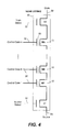
- FIG. 4 illustrates schematically a string of memory cells organized into a NAND string.
- a pair of select transistors S 1 , S 2 controls the memory transistor chain's connection to the external world via the NAND string's source terminal 54 and drain terminal 56 respectively.
- the source select transistor 51 when the source select transistor 51 is turned on, the source terminal is coupled to a source line (see FIG. 5 ).
- the drain select transistor S 2 is turned on, the drain terminal of the NAND string is coupled to a bit line of the memory array.
- Each memory transistor 10 in the chain acts as a memory cell. It has a charge storage element 20 to store a given amount of charge so as to represent an intended memory state.
- a control gate 30 of each memory transistor allows control over read and write operations. As will be seen in FIG. 5 , the control gates 30 of corresponding memory transistors of a row of NAND string are all connected to the same word line. Similarly, a control gate 32 of each of the select transistors S 1 , S 2 provides control access to the NAND string via its source terminal 54 and drain terminal 56 respectively. Likewise, the control gates 32 of corresponding select transistors of a row of NAND string are all connected to the same select line.
- FIG. 5 illustrates an example of a NAND array 210 of memory cells, constituted from NAND strings 50 such as that shown in FIG. 4 .
- a bit line such as bit line 36 is coupled to the drain terminal 56 of each NAND string.
- a source line such as source line 34 is coupled to the source terminals 54 of each NAND string.
- the control gates along a row of memory cells in a bank of NAND strings are connected to a word line such as word line 42 .
- the control gates along a row of select transistors in a bank of NAND strings are connected to a select line such as select line 44 .
- An entire row of memory cells in a bank of NAND strings can be addressed by appropriate voltages on the word lines and select lines of the bank of NAND strings.
- FIG. 6 illustrates a page of memory cells, organized in the NAND configuration, being sensed or programmed in parallel.
- FIG. 6 essentially shows a bank of NAND strings 50 in the memory array 210 of FIG. 5 , where the detail of each NAND string is shown explicitly as in FIG. 4 .
- a physical page such as the page 60 , is a group of memory cells enabled to be sensed or programmed in parallel. This is accomplished by a corresponding page of sense amplifiers 212 . The sensed results are latched in a corresponding set of latches 214 .
- Each sense amplifier can be coupled to a NAND string via a bit line.
- the page is enabled by the control gates of the cells of the page connected in common to a word line 42 and each cell accessible by a sense amplifier accessible via a bit line 36 .
- a sensing voltage or a programming voltage is respectively applied to the common word line WL 3 together with appropriate voltages on the bit lines.
- flash memory One important difference between flash memory and other of types of memory is that a cell must be programmed from the erased state. That is the floating gate must first be emptied of charge. Programming then adds a desired amount of charge back to the floating gate. It does not support removing a portion of the charge from the floating gate to go from a more programmed state to a lesser one. This means that updated data cannot overwrite existing data and must be written to a previous unwritten location.
- the array of memory cells is divided into a large number of blocks of memory cells.
- the block is the unit of erase. That is, each block contains the minimum number of memory cells that are erased together. While aggregating a large number of cells in a block to be erased in parallel will improve erase performance, a large size block also entails dealing with a larger number of update and obsolete data.
- Each block is typically divided into a number of physical pages.
- a logical page is a unit of programming or reading that contains a number of bits equal to the number of cells in a physical page.
- one physical page stores one logical page of data.
- a physical page stores two logical pages. The number of logical pages stored in a physical page thus reflects the number of bits stored per cell.
- the individual pages may be divided into segments and the segments may contain the fewest number of cells that are written at one time as a basic programming operation.
- One or more logical pages of data are typically stored in one row of memory cells.
- a page can store one or more sectors.
- a sector includes user data and overhead data.
- FIGS. 7A-7C illustrate an example of programming a population of 4-state memory cells.
- FIG. 7A illustrates the population of memory cells programmable into four distinct distributions of threshold voltages respectively representing memory states “0”, “1”, “2” and “3”.
- FIG. 7B illustrates the initial distribution of “erased” threshold voltages for an erased memory.
- FIG. 7C illustrates an example of the memory after many of the memory cells have been programmed. Essentially, a cell initially has an “erased” threshold voltage and programming will move it to a higher value into one of the three zones demarcated by verify levels vV 1 , vV 2 and vV 3 .
- each memory cell can be programmed to one of the three programmed states “1”, “2” and “3” or remain un-programmed in the “erased” state.
- the initial distribution of the “erased” state as shown in FIG. 7B will become narrower and the erased state is represented by the “0” state.
- a 2-bit code having a lower bit and an upper bit can be used to represent each of the four memory states.
- the “0”, “1”, “2” and “3” states are respectively represented by “11”, “01”, “00” and ‘10”.
- the 2-bit data may be read from the memory by sensing in “full-sequence” mode where the two bits are sensed together by sensing relative to the read demarcation threshold values rV 1 , rV 2 and rV 3 in three sub-passes respectively.
- An alternative arrangement to a conventional two-dimensional (2-D) NAND array is a three-dimensional (3-D) array.
- 3-D arrays extend up from the wafer surface and generally include stacks, or columns, of memory cells extending upwards.
- Various 3-D arrangements are possible.
- a NAND string is formed vertically with one end (e.g. source) at the wafer surface and the other end (e.g. drain) on top.
- a NAND string is formed in a U-shape so that both ends of the NAND string are accessible on top, thus facilitating connections between such strings. Examples of such NAND strings and their formation are described in U.S. Patent Publication Number 2012/0220088 and in U.S. Patent Publication Number 2013/0107628, which are hereby incorporated by reference in their entirety.
- FIG. 8 shows a first example of a NAND string 701 that extends in a vertical direction, i.e. extending in the z-direction, perpendicular to the x-y plane of the substrate.
- Memory cells are formed where a vertical bit line (local bit line) 703 passes through a word line (e.g. WL 0 , WL 1 , etc.).
- a charge trapping layer between the local bit line and the word line stores charge, which affects the threshold voltage of the transistor formed by the word line (gate) coupled to the vertical bit line (channel) that it encircles.
- Such memory cells may be formed by forming stacks of word lines and then etching memory holes where memory cells are to be formed. Memory holes are then lined with a charge trapping layer and filled with a suitable local bit line/channel material (with suitable dielectric layers for isolation).
- select gates 705 , 707 are located at either end of the string to allow the NAND string to be selectively connected to, or isolated from, external elements 709 , 711 .
- external elements are generally conductive lines such as common source lines or bit lines that serve large numbers of NAND strings.
- Vertical NAND strings may be operated in a similar manner to planar NAND strings and both SLC and MLC operation is possible. While FIG. 8 shows an example of a NAND string that has 32 cells ( 0 - 31 ) connected in series, the number of cells in a NAND string may be any suitable number. Not all cells are shown for clarity. It will be understood that additional cells are formed where word lines 3 - 29 (not shown) intersect the local vertical bit line.
- a 3D NAND array can, loosely speaking, be formed tilting up the respective structures 50 and 210 of FIGS. 5 and 6 to be perpendicular to the x-y plane.
- each y-z plane corresponds to the page structure of FIG. 6 , with m such plane at differing x locations.
- the (global) bit lines, BL 1 - m each run across the top to an associated sense amp SA 1 - m .
- the word lines, WL 1 - n , and source and select lines SSL 1 - n and DSL 1 - n then run in x direction, with the NAND string connected at bottom to a common source line CSL.
- FIGS. 9-12 look at a particular monolithic three dimensional (3D) memory array of the NAND type (more specifically of the “BiCS” type), where one or more memory device levels are formed above a single substrate, in more detail.
- FIG. 9 is an oblique projection of part of such a structure, showing a portion corresponding to two of the page structures in FIG. 5 , where, depending on the embodiment, each of these could correspond to a separate block or be different “fingers” of the same block.
- the NAND strings lying in a common y-z plane they are squashed together in the y direction, so that the NAND strings are somewhat staggered in the x direction.
- the NAND strings are connected along global bit lines (BL) spanning multiple such sub-divisions of the array that run in the x direction.
- global common source lines also run across multiple such structures in the x direction and are connect to the sources at the bottoms of the NAND string, which are connected by a local interconnect (LI) that serves as the local common source line of the individual finger.
- LI local interconnect
- the global source lines can span the whole, or just a portion, of the array structure.
- variations can include the NAND string being formed in a U type structure, where part of the string itself runs back up, such as is described in U.S.
- FIG. 9 To the right of FIG. 9 is a representation of the elements of one of the vertical NAND strings from the structure to the left.
- Multiple memory cells are connected through a drain select gate SGD to the associated bit line BL at the top and connected through the associated source select gate SDS to the associated local source line LI to a global source line SL.
- a select gate with a greater length than that of memory cells, where this can alternately be achieved by having several select gates in series (as described in U.S. patent application Ser. No. 13/925,662, filed on Jun. 24, 2013), making for more uniform processing of layers.
- the select gates are programmable to have their threshold levels adjusted, aspects of which are described in US patent publication number 2014-0169095.
- This exemplary embodiment also includes several dummy cells at the ends that are not used to store user data, as their proximity to the select gates makes them more prone to disturbs.
- FIG. 10 shows a top view of the structure for two blocks in the exemplary embodiment.
- Two blocks (BLK 0 above, BLK 1 below) are shown, each having four fingers that run left to right.
- the word lines and select gate lines of each level also run left to right, with the word lines of the different fingers of the same block being commonly connected at a “terrace” and then on to receive their various voltage level through the word line select gates at WLTr.
- the word lines of a given layer in a block can also be commonly connected on the far side from the terrace.
- the selected gate lines can be individual for each level, rather common, allowing the fingers to be individually selected.
- the bit lines are shown running up and down the page and connect on to the sense amp circuits, where, depending on the embodiment, each sense amp can correspond to a single bit line or be multiplexed to several bit lines.
- FIG. 11 shows a side view of one block, again with four fingers.
- the select gates SGD and SGS at either end of the NAND strings are formed of four layers, with the word lines WL in-between, all formed over a CPWELL.
- a given finger is selected by setting its select gates to a level VSG and the word lines are biased according to the operation, such as a read voltage (VCGRV) for the selected word lines and the read-pass voltage (VREAD) for the non-selected word lines.
- the non-selected fingers can then be cut off by setting their select gates accordingly.
- FIG. 12 illustrates some detail of an individual cell.
- a dielectric core runs in the vertical direction and is surrounded by a channel silicon layer, that is in turn surrounded a tunnel dielectric (TNL) and then the charge trapping dielectric layer (CTL).
- TNL tunnel dielectric
- CTL charge trapping dielectric layer
- the gate of the cell is here framed of tungsten with which is surrounded by a metal barrier and is separated from the charge trapping layer by blocking (BLK) oxide and a high K layer.
- BLK blocking
- the sort of memory structure described with respect to FIGS. 9-12 present a memory structure having a NAND type of architecture in which the select gates are programmable.
- This section considers techniques for programming these select gates.
- the select gates differ from the memory cells, among other ways, in that they are directly connected to either the bit line on the one end of the NAND string or to the source line on the other, whereas the memory cells have these select gates separating them from these lines to be used to control the bias levels to the memory cells.
- Vt threshold voltage
- the select gates differ in that they have their Vt programmed in order allow them to properly perform their function, as opposed to storing data values.
- FIG. 13 shows a typical set of bias waveforms for programming selected memory cells in a NAND type memory.
- the source (SGS) and drain (SGD) side select gates are set low to ground (VSS), as are the bit lines (BL) corresponding to cells to be programmed, while program disabled bit lines are set to a VBL level (2V in this example) and the source line is set at VSL (here 1.5V).
- the non-selected word lines are then taken to VPASS and the selected word lines up to the full program voltage of VPGM.
- FIG. 13 shows a typical set of bias waveforms for programming selected memory cells in a NAND type memory.
- the source (SGS) and drain (SGD) side select gates are set low to ground (VSS), as are the bit lines (BL) corresponding to cells to be programmed, while program disabled bit lines are set to a VBL level (2V in this example) and the source line is set at VSL (here 1.5V).
- VSL here 1.5V
- the select gates are off, the channel is boosted, and programming occurs. If, instead, the selects were to have a negative threshold voltage (SG Vt ⁇ 0V) as illustrated in FIG. 14B , they will conduct even though their gates are at 0V, and the selected memory cells will not program properly.
- SG Vt ⁇ 0V negative threshold voltage
- FIG. 15 shows an exemplary set of bias voltages for selected and unselected word line, source and drain select gates, bit lines and source lines for a selected string in a selected block (top), an unselected string in a selected block (middle), and unselected string from unselected blocks (bottom).
- both source and drain selects should be on (at VSG) so the selected cells can be read; but for unselected strings in both selected and unselected blocks, the select gates are set biased at VSS so that they are turned off and will not contributed to the result of the sensing operation.
- FIG. 16 illustrates the mechanism in the BiCS context: here, the string at the left of the left most finger is selected, with any current flowing off to the source line CELSR, as indicated by the arrow. However, if the strings along the same bit line of the other fingers are not fully cut off by their select gates, they may also have some current flowing, as indicated at the lighter arrows, affecting the sensing result.
- FIG. 17 is a two dimensional projection of a block of a typical BiCS type structure, showing one NAND string sharing a common bit line for each of four finger, to illustrate some of the structure on how the select gates and memory cells are arranged.
- Each finger has its individually controllable set of drain select gates, SCG 0 - 3 , and source select gates, SGS 0 - 3 , along with the common source gate.
- the word lines WL 0 - n then run across all four fingers.
- the select gates can then be programmed similarly to the process for memory cells, but with some differences.
- programming pulses are applied to the control gates (now by way of the select lines, rather than word lines) with intervening verify operations, but where these are a collective verify for the commonly controlled sets of select gates; that is, the four select gates all controlled by SGD 0 would be verified as a unit, where they are being programmed to tune their threshold voltage as opposed to storing a data value.
- a difficulty in programming these sets of select gates is that, unlike the memory cells along the word lines, they are not separated from the bit line BL by a separate select gate on the drain end nor are they separated from the source line on the other end.
- This lack of a “select gate for the select gates” make it difficult to set the proper bias levels allowing the select gates to be programmed in the same way as the memory cells. For instance, on the drain side this means that the bit line needs to be biased to higher level that is typically provided by the sense amp in order to inhibit programming, requiring an elevated level from a charge pump. And the common SGC line and CELSRC level does not allow for inhibiting the source side selected transistors of individual fingers. Also, due the amount of coupling due to the density of the BiCS structure, it is often difficult to program along all of the bit lines, whether for word lines or select gates together, so that only every other or even every fourth bit line is done concurrently.
- the exemplary embodiment uses a modified structure for the select gates.
- the end select gate connected to the bit line is separately controllable from the other drain side select gates, allowing to be used more typically like a drain side select gate during the programming of the other drain side select gates, which can still be commonly controlled.
- the end select gate connected to the local common source line is also controllable separately from the other source side select gates, allowing it to be biased separately for programming of the other source select gates.
- FIG. 18 which can be compared to FIG. 17 . The levels shown are for programming the three drain select transistors on the right most NAND string.
- FIG. 18 four NAND strings, one each from four fingers of a block, are shown.
- the three select gates adjacent to the word lines in each finger again have commonly connected control gates.
- the end most drain select gate, through which the finger connects to the bit line BL, is controlled separately.
- the end select gates of the four fingers are all connected along the same control line SGD 4 .
- a similar structure is used along the bottom, with the bottom transistors of the four fingers, through which each NAND strings connects to the local source line, commonly connected along control line SGS 4 , which also controls the transistors between the NAND strings and the source line inter-connect columns.
- each NAND string has four select gates on either end of each NAND string, where the end-most of each set is controlled independently of the other three, which are commonly controlled, but the techniques of the is section are more generally applicable.
- one or more end-most select transistors can serve a more or less standard select gate function while programming of one or more additional select transistors with adjustable thresholds to the inside, where this can be implemented independently on either the source or drain sides. Consequently, the threshold tuning of select gates' threshold becomes similar to the programming of memory cells, but where (when there is more than one of such adjustable Vt select gates) the verify is a combined verify and rather than being written to a data state they are having there thresholds set to a well-defined level to allow proper operation of the NAND string.
- all of the word lines are treated as unselected and set at the programming pass level VPASS (typically on the order of 10V), as are the levels SGD 0 - 2 on the drain side select gates of non-selected fingers.
- the source side select gate level SGS 0 - 3 are set to VSGS, a level sufficient to turn them on.
- the end source side select gate line SGS 4 is set to VSS (0V) to shut off the NAND string on the source end and also the gates between local source line interconnects.
- the end most drain side select gate control line SGD 4 is then set at VSGD, a value so that it either conducts or is off based on whether the bit line is program inhibited or program enabled; for example, something like 4V.
- the bit line BL is set at VSS and to program inhibit the bit line is raised to a high level from the sense amp, here a level VDDSA used for pre-charging bit lines that can be in the 2.5V-4V range.
- CELSRC is set high (such as VDDSA) to shut off the transistors, and once verified or if non-selected CELSRC can be set at the threshold voltage of a depleted device, Vtd (.about.1V), to turn on the transistors.
- the bit line is set to the program enable level (VSS).
- VSS program enable level
- the VBOOST does not need to be particularly large in SGD programming (.about.3 v to 4 v range) and a largely conventional programming process can be used.
- an all bit line program can be done for the select gates to improve performance, whereas for the memory cells only every other or every fourth bit line are programmed concurrently in the BiCS type structure due to the amount of capacitive coupling the results from high density structure.
- the others can be programmed without need of a charge pump to pre-charge bit lines to a higher than standard level, saving on power.
- FIG. 20 is similar to FIG. 18 , but for programming of the source side select gates.
- the biasing is largely as before, except that now on the selected (right most) NAND string, the commonly connected drain side select gates are also now at VPASS to provide channel boosting.
- FIG. 21 that is source side equivalent of FIG. 19 .
- the commonly connected gates of the source select gates then receive the programming pulses, alternated with a common verify operation. This can provide the same advantages as for the drain side process in terms of speed, power and accuracy, allowing for the individual programming of each finger's source side select gates.
Landscapes
- Engineering & Computer Science (AREA)
- Microelectronics & Electronic Packaging (AREA)
- Computer Hardware Design (AREA)
- Semiconductor Memories (AREA)
- Read Only Memory (AREA)
- Non-Volatile Memory (AREA)
Abstract
Description
Claims (20)
Priority Applications (1)
| Application Number | Priority Date | Filing Date | Title |
|---|---|---|---|
| US15/599,850 US9947407B2 (en) | 2014-08-20 | 2017-05-19 | Techniques for programming of select gates in NAND memory |
Applications Claiming Priority (3)
| Application Number | Priority Date | Filing Date | Title |
|---|---|---|---|
| US14/464,122 US9305648B2 (en) | 2014-08-20 | 2014-08-20 | Techniques for programming of select gates in NAND memory |
| US15/062,987 US9659656B2 (en) | 2014-08-20 | 2016-03-07 | Techniques for programming of select gates in NAND memory |
| US15/599,850 US9947407B2 (en) | 2014-08-20 | 2017-05-19 | Techniques for programming of select gates in NAND memory |
Related Parent Applications (1)
| Application Number | Title | Priority Date | Filing Date |
|---|---|---|---|
| US15/062,987 Continuation US9659656B2 (en) | 2014-08-20 | 2016-03-07 | Techniques for programming of select gates in NAND memory |
Publications (2)
| Publication Number | Publication Date |
|---|---|
| US20170256317A1 US20170256317A1 (en) | 2017-09-07 |
| US9947407B2 true US9947407B2 (en) | 2018-04-17 |
Family
ID=55348833
Family Applications (3)
| Application Number | Title | Priority Date | Filing Date |
|---|---|---|---|
| US14/464,122 Expired - Fee Related US9305648B2 (en) | 2014-08-20 | 2014-08-20 | Techniques for programming of select gates in NAND memory |
| US15/062,987 Active US9659656B2 (en) | 2014-08-20 | 2016-03-07 | Techniques for programming of select gates in NAND memory |
| US15/599,850 Active US9947407B2 (en) | 2014-08-20 | 2017-05-19 | Techniques for programming of select gates in NAND memory |
Family Applications Before (2)
| Application Number | Title | Priority Date | Filing Date |
|---|---|---|---|
| US14/464,122 Expired - Fee Related US9305648B2 (en) | 2014-08-20 | 2014-08-20 | Techniques for programming of select gates in NAND memory |
| US15/062,987 Active US9659656B2 (en) | 2014-08-20 | 2016-03-07 | Techniques for programming of select gates in NAND memory |
Country Status (1)
| Country | Link |
|---|---|
| US (3) | US9305648B2 (en) |
Cited By (4)
| Publication number | Priority date | Publication date | Assignee | Title |
|---|---|---|---|---|
| US20170162257A1 (en) * | 2015-12-04 | 2017-06-08 | Kabushiki Kaisha Toshiba | Memory device |
| US10896711B2 (en) | 2018-12-21 | 2021-01-19 | Samsung Electronics Co., Ltd. | Memory device with memory cell structure including ferroelectric data storage layer, and a first gate and a second gate |
| US12046294B2 (en) | 2022-06-23 | 2024-07-23 | Sandisk Technologies Llc | Non-volatile memory with short prevention |
| US12154630B2 (en) | 2022-06-03 | 2024-11-26 | Sandisk Technologies Llc | Non-volatile memory with tuning of erase process |
Families Citing this family (26)
| Publication number | Priority date | Publication date | Assignee | Title |
|---|---|---|---|---|
| KR20150047285A (en) * | 2013-10-24 | 2015-05-04 | 에스케이하이닉스 주식회사 | Semiconductor device, manufacturing method and operating method thereof |
| US9305648B2 (en) | 2014-08-20 | 2016-04-05 | SanDisk Technologies, Inc. | Techniques for programming of select gates in NAND memory |
| KR102272238B1 (en) * | 2014-09-02 | 2021-07-06 | 삼성전자주식회사 | Nonvolatile memory device and programming method thereof |
| US9356074B1 (en) * | 2014-11-17 | 2016-05-31 | Sandisk Technologies Inc. | Memory array having divided apart bit lines and partially divided bit line selector switches |
| KR20160062498A (en) * | 2014-11-25 | 2016-06-02 | 에스케이하이닉스 주식회사 | Semiconductor memory device and operating method thereof |
| JP6470146B2 (en) * | 2015-08-27 | 2019-02-13 | 東芝メモリ株式会社 | Semiconductor memory device |
| KR102320830B1 (en) * | 2015-09-24 | 2021-11-03 | 에스케이하이닉스 주식회사 | Semiconductor memory device including three-dimensional array structure |
| JP6581019B2 (en) | 2016-03-02 | 2019-09-25 | 東芝メモリ株式会社 | Semiconductor memory device |
| TWI765122B (en) * | 2016-08-18 | 2022-05-21 | 日商鎧俠股份有限公司 | semiconductor device |
| US9972641B1 (en) * | 2016-11-17 | 2018-05-15 | Sandisk Technologies Llc | Three-dimensional memory device having a multilevel drain select gate electrode and method of making thereof |
| US10083982B2 (en) * | 2016-11-17 | 2018-09-25 | Sandisk Technologies Llc | Three-dimensional memory device having select gate electrode that is thicker than word lines and method of making thereof |
| US9842657B1 (en) * | 2017-05-18 | 2017-12-12 | Sandisk Technologies Llc | Multi-state program using controlled weak boosting for non-volatile memory |
| US10573388B2 (en) | 2018-04-04 | 2020-02-25 | Western Digital Technologies, Inc. | Non-volatile storage system with adjustable select gates as a function of temperature |
| US10566059B2 (en) * | 2018-04-30 | 2020-02-18 | Sandisk Technologies Llc | Three dimensional NAND memory device with drain select gate electrode shared between multiple strings |
| US10978152B1 (en) * | 2019-11-13 | 2021-04-13 | Sandisk Technologies Llc | Adaptive VPASS for 3D flash memory with pair string structure |
| EP3832721A1 (en) * | 2019-12-06 | 2021-06-09 | Imec VZW | A method for fabricating a 3d ferroelectric memory |
| US11489043B2 (en) | 2020-04-27 | 2022-11-01 | Sandisk Technologies Llc | Three-dimensional memory device employing thinned insulating layers and methods for forming the same |
| WO2021221738A1 (en) * | 2020-04-27 | 2021-11-04 | Sandisk Technologies Llc | Three-dimensional memory device employing thinned insulating layers and methods for forming the same |
| DE102021106752B4 (en) * | 2020-05-29 | 2023-10-26 | Taiwan Semiconductor Manufacturing Company, Ltd. | MEMORY DEVICE, INTEGRATED CIRCUIT DEVICE AND METHOD |
| JP7404203B2 (en) | 2020-09-17 | 2023-12-25 | キオクシア株式会社 | semiconductor storage device |
| WO2022178426A1 (en) * | 2021-02-21 | 2022-08-25 | The Regents Of The University Of California | Roll-to-roll based 3d printing through computed axial lithography |
| DE102022102588A1 (en) * | 2021-06-28 | 2022-12-29 | Sandisk Technologies Llc | SIMULTANEOUS PROGRAMMING OF MULTIPLE CELLS FOR NON-VOLATILE STORAGE DEVICES |
| US12080351B2 (en) * | 2021-10-07 | 2024-09-03 | Micron Technology, Inc. | Using non-segregated cells as drain-side select gates for sub-blocks in a memory device |
| US12014785B2 (en) * | 2021-10-27 | 2024-06-18 | Sandisk Technologies Llc | Adaptive semi-circle select gate bias |
| KR20240048176A (en) * | 2022-10-06 | 2024-04-15 | 에스케이하이닉스 주식회사 | Nonvolatile memory device including selection transistors and operation method thereof |
| CN119785854B (en) * | 2023-10-08 | 2025-11-11 | 长江存储科技有限责任公司 | Memory device, operation method thereof and memory system |
Citations (36)
| Publication number | Priority date | Publication date | Assignee | Title |
|---|---|---|---|---|
| US5070032A (en) | 1989-03-15 | 1991-12-03 | Sundisk Corporation | Method of making dense flash eeprom semiconductor memory structures |
| US5095344A (en) | 1988-06-08 | 1992-03-10 | Eliyahou Harari | Highly compact eprom and flash eeprom devices |
| US5313421A (en) | 1992-01-14 | 1994-05-17 | Sundisk Corporation | EEPROM with split gate source side injection |
| US5315541A (en) | 1992-07-24 | 1994-05-24 | Sundisk Corporation | Segmented column memory array |
| US5332917A (en) * | 1992-12-28 | 1994-07-26 | Samsung Electronics Co., Ltd. | Semiconductor memory NAND with wide space between selection lines |
| US5343063A (en) | 1990-12-18 | 1994-08-30 | Sundisk Corporation | Dense vertical programmable read only memory cell structure and processes for making them |
| US5570315A (en) | 1993-09-21 | 1996-10-29 | Kabushiki Kaisha Toshiba | Multi-state EEPROM having write-verify control circuit |
| US5602789A (en) | 1991-03-12 | 1997-02-11 | Kabushiki Kaisha Toshiba | Electrically erasable and programmable non-volatile and multi-level memory systemn with write-verify controller |
| US5661053A (en) | 1994-05-25 | 1997-08-26 | Sandisk Corporation | Method of making dense flash EEPROM cell array and peripheral supporting circuits formed in deposited field oxide with the use of spacers |
| US5673222A (en) | 1995-06-20 | 1997-09-30 | Sharp Kabushiki Kaisha | Nonvolatile semiconductor memory device |
| US5768192A (en) | 1996-07-23 | 1998-06-16 | Saifun Semiconductors, Ltd. | Non-volatile semiconductor memory cell utilizing asymmetrical charge trapping |
| US5903495A (en) | 1996-03-18 | 1999-05-11 | Kabushiki Kaisha Toshiba | Semiconductor device and memory system |
| US6011725A (en) | 1997-08-01 | 2000-01-04 | Saifun Semiconductors, Ltd. | Two bit non-volatile electrically erasable and programmable semiconductor memory cell utilizing asymmetrical charge trapping |
| US6222762B1 (en) | 1992-01-14 | 2001-04-24 | Sandisk Corporation | Multi-state memory |
| US20060279992A1 (en) | 2005-05-11 | 2006-12-14 | Samsung Electronics Co., Ltd. | NAND flash memory devices having shielding lines between wordlines and selection lines |
| US7433231B2 (en) | 2006-04-26 | 2008-10-07 | Micron Technology, Inc. | Multiple select gates with non-volatile memory cells |
| US7470948B2 (en) * | 2006-03-07 | 2008-12-30 | Samsung Electronics Co., Ltd. | Memory cell array structures in NAND flash memory devices |
| US20100002516A1 (en) * | 2008-07-02 | 2010-01-07 | Samsung Electronics Co., Ltd. | Integrated Circuit Memory Devices Having Vertically Arranged Strings of Memory Cells Therein and Methods of Operating Same |
| US20100315875A1 (en) | 2009-02-02 | 2010-12-16 | Samsung Electronics Co., Ltd. | Non-volatile memory device having vertical structure and method of operating the same |
| US20140003157A1 (en) | 2012-06-28 | 2014-01-02 | Sandisk Technologies Inc. | Compact High Speed Sense Amplifier for Non-Volatile Memory and Hybrid Lockout |
| US20140169095A1 (en) | 2012-12-18 | 2014-06-19 | Sandisk Technologies Inc. | Select Transistor Tuning |
| US20140293702A1 (en) | 2013-04-02 | 2014-10-02 | Sandisk Technologies Inc. | Select Gate Materials Having Different Work Functions In Non-Volatile Memory |
| US8933516B1 (en) | 2013-06-24 | 2015-01-13 | Sandisk 3D Llc | High capacity select switches for three-dimensional structures |
| US9053796B2 (en) | 2013-10-24 | 2015-06-09 | SK Hynix Inc. | Semiconductor device and methods of manufacturing and operating the same |
| US9099202B2 (en) | 2012-11-06 | 2015-08-04 | Sandisk Technologies Inc. | 3D stacked non-volatile storage programming to conductive state |
| US20150228352A1 (en) * | 2014-02-07 | 2015-08-13 | SK Hynix Inc. | Semiconductor memory device and memory system including the same |
| US9147471B2 (en) * | 2011-11-08 | 2015-09-29 | Samsung Electronics Co., Ltd. | Nonvolatile memory device and driving method thereof |
| US9196365B2 (en) * | 2013-12-19 | 2015-11-24 | SK Hynix Inc. | Semiconductor memory device and operating method thereof |
| US9230656B2 (en) | 2013-06-26 | 2016-01-05 | Sandisk Technologies Inc. | System for maintaining back gate threshold voltage in three dimensional NAND memory |
| US9275743B1 (en) * | 2014-08-20 | 2016-03-01 | SK Hynix Inc. | Semiconductor memory device and operating method thereof |
| US9305648B2 (en) | 2014-08-20 | 2016-04-05 | SanDisk Technologies, Inc. | Techniques for programming of select gates in NAND memory |
| US20160099060A1 (en) * | 2014-10-02 | 2016-04-07 | SK Hynix Inc. | Semiconductor memory device including a dummy memory cell and method of programming the same |
| US9318201B2 (en) * | 2014-07-10 | 2016-04-19 | SK Hynix Inc. | Semiconductor memory device including three-dimensional array structure |
| US9384841B2 (en) * | 2014-05-26 | 2016-07-05 | SK Hynix Inc. | Semiconductor device, semiconductor system having the same and operating method thereof |
| US9396799B2 (en) * | 2014-11-19 | 2016-07-19 | SK Hynix Inc. | Semiconductor memory device improving threshold voltage of unselected memory block and method of operating the same |
| US9767906B2 (en) * | 2015-09-24 | 2017-09-19 | SK Hynix Inc. | Semiconductor memory device including three-dimensional array structure and memory system including the same |
-
2014
- 2014-08-20 US US14/464,122 patent/US9305648B2/en not_active Expired - Fee Related
-
2016
- 2016-03-07 US US15/062,987 patent/US9659656B2/en active Active
-
2017
- 2017-05-19 US US15/599,850 patent/US9947407B2/en active Active
Patent Citations (43)
| Publication number | Priority date | Publication date | Assignee | Title |
|---|---|---|---|---|
| US5095344A (en) | 1988-06-08 | 1992-03-10 | Eliyahou Harari | Highly compact eprom and flash eeprom devices |
| US5070032A (en) | 1989-03-15 | 1991-12-03 | Sundisk Corporation | Method of making dense flash eeprom semiconductor memory structures |
| US5343063A (en) | 1990-12-18 | 1994-08-30 | Sundisk Corporation | Dense vertical programmable read only memory cell structure and processes for making them |
| US5602789A (en) | 1991-03-12 | 1997-02-11 | Kabushiki Kaisha Toshiba | Electrically erasable and programmable non-volatile and multi-level memory systemn with write-verify controller |
| US6222762B1 (en) | 1992-01-14 | 2001-04-24 | Sandisk Corporation | Multi-state memory |
| US5313421A (en) | 1992-01-14 | 1994-05-17 | Sundisk Corporation | EEPROM with split gate source side injection |
| US5315541A (en) | 1992-07-24 | 1994-05-24 | Sundisk Corporation | Segmented column memory array |
| US5332917A (en) * | 1992-12-28 | 1994-07-26 | Samsung Electronics Co., Ltd. | Semiconductor memory NAND with wide space between selection lines |
| US5570315A (en) | 1993-09-21 | 1996-10-29 | Kabushiki Kaisha Toshiba | Multi-state EEPROM having write-verify control circuit |
| US5661053A (en) | 1994-05-25 | 1997-08-26 | Sandisk Corporation | Method of making dense flash EEPROM cell array and peripheral supporting circuits formed in deposited field oxide with the use of spacers |
| US5673222A (en) | 1995-06-20 | 1997-09-30 | Sharp Kabushiki Kaisha | Nonvolatile semiconductor memory device |
| US5903495A (en) | 1996-03-18 | 1999-05-11 | Kabushiki Kaisha Toshiba | Semiconductor device and memory system |
| US6046935A (en) | 1996-03-18 | 2000-04-04 | Kabushiki Kaisha Toshiba | Semiconductor device and memory system |
| US5768192A (en) | 1996-07-23 | 1998-06-16 | Saifun Semiconductors, Ltd. | Non-volatile semiconductor memory cell utilizing asymmetrical charge trapping |
| US6011725A (en) | 1997-08-01 | 2000-01-04 | Saifun Semiconductors, Ltd. | Two bit non-volatile electrically erasable and programmable semiconductor memory cell utilizing asymmetrical charge trapping |
| US20060279992A1 (en) | 2005-05-11 | 2006-12-14 | Samsung Electronics Co., Ltd. | NAND flash memory devices having shielding lines between wordlines and selection lines |
| US7470948B2 (en) * | 2006-03-07 | 2008-12-30 | Samsung Electronics Co., Ltd. | Memory cell array structures in NAND flash memory devices |
| US7433231B2 (en) | 2006-04-26 | 2008-10-07 | Micron Technology, Inc. | Multiple select gates with non-volatile memory cells |
| US20100002516A1 (en) * | 2008-07-02 | 2010-01-07 | Samsung Electronics Co., Ltd. | Integrated Circuit Memory Devices Having Vertically Arranged Strings of Memory Cells Therein and Methods of Operating Same |
| US8488381B2 (en) * | 2009-02-02 | 2013-07-16 | Samsung Electronics Co., Ltd. | Non-volatile memory device having vertical structure and method of operating the same |
| US20100315875A1 (en) | 2009-02-02 | 2010-12-16 | Samsung Electronics Co., Ltd. | Non-volatile memory device having vertical structure and method of operating the same |
| US9601208B2 (en) * | 2011-11-08 | 2017-03-21 | Samsung Electronics Co., Ltd. | Nonvolatile memory device and driving method thereof |
| US9147471B2 (en) * | 2011-11-08 | 2015-09-29 | Samsung Electronics Co., Ltd. | Nonvolatile memory device and driving method thereof |
| US20140003157A1 (en) | 2012-06-28 | 2014-01-02 | Sandisk Technologies Inc. | Compact High Speed Sense Amplifier for Non-Volatile Memory and Hybrid Lockout |
| US9099202B2 (en) | 2012-11-06 | 2015-08-04 | Sandisk Technologies Inc. | 3D stacked non-volatile storage programming to conductive state |
| US20140169095A1 (en) | 2012-12-18 | 2014-06-19 | Sandisk Technologies Inc. | Select Transistor Tuning |
| US9123425B2 (en) * | 2013-04-02 | 2015-09-01 | Sandisk Technologies Inc. | Adjusting control gate overdrive of select gate transistors during programming of non-volatile memory |
| US20140293702A1 (en) | 2013-04-02 | 2014-10-02 | Sandisk Technologies Inc. | Select Gate Materials Having Different Work Functions In Non-Volatile Memory |
| US20140293701A1 (en) | 2013-04-02 | 2014-10-02 | Sandisk Technologies Inc. | Adjusting Control Gate Overdrive Of Select Gate Transistors During Programming Of Non-Volatile Memory |
| US8964473B2 (en) * | 2013-04-02 | 2015-02-24 | Sandisk Technologies Inc. | Select gate materials having different work functions in non-volatile memory |
| US8933516B1 (en) | 2013-06-24 | 2015-01-13 | Sandisk 3D Llc | High capacity select switches for three-dimensional structures |
| US9230656B2 (en) | 2013-06-26 | 2016-01-05 | Sandisk Technologies Inc. | System for maintaining back gate threshold voltage in three dimensional NAND memory |
| US9053796B2 (en) | 2013-10-24 | 2015-06-09 | SK Hynix Inc. | Semiconductor device and methods of manufacturing and operating the same |
| US9196365B2 (en) * | 2013-12-19 | 2015-11-24 | SK Hynix Inc. | Semiconductor memory device and operating method thereof |
| US20150228352A1 (en) * | 2014-02-07 | 2015-08-13 | SK Hynix Inc. | Semiconductor memory device and memory system including the same |
| US9384841B2 (en) * | 2014-05-26 | 2016-07-05 | SK Hynix Inc. | Semiconductor device, semiconductor system having the same and operating method thereof |
| US9318201B2 (en) * | 2014-07-10 | 2016-04-19 | SK Hynix Inc. | Semiconductor memory device including three-dimensional array structure |
| US9275743B1 (en) * | 2014-08-20 | 2016-03-01 | SK Hynix Inc. | Semiconductor memory device and operating method thereof |
| US9305648B2 (en) | 2014-08-20 | 2016-04-05 | SanDisk Technologies, Inc. | Techniques for programming of select gates in NAND memory |
| US20160189778A1 (en) | 2014-08-20 | 2016-06-30 | SanDisk Technologies, Inc. | Techniques for programming of select gates in nand memory |
| US20160099060A1 (en) * | 2014-10-02 | 2016-04-07 | SK Hynix Inc. | Semiconductor memory device including a dummy memory cell and method of programming the same |
| US9396799B2 (en) * | 2014-11-19 | 2016-07-19 | SK Hynix Inc. | Semiconductor memory device improving threshold voltage of unselected memory block and method of operating the same |
| US9767906B2 (en) * | 2015-09-24 | 2017-09-19 | SK Hynix Inc. | Semiconductor memory device including three-dimensional array structure and memory system including the same |
Non-Patent Citations (8)
| Title |
|---|
| Amendment under 37 CFR 1.312 dated Feb. 12, 2016, U.S. Appl. No. 14/464,122, filed Aug. 20, 2014. |
| Eitan, et al., "NROM: A Novel Localized Trapping, 2-Bit Nonvolatile Memory Cell," IEEE Electron Device Letters, vol. 21, No. 11, Nov. 2000, pp. 543-545. |
| Ex Parte Quayle dated Aug. 6, 2015, U.S. Appl. No. 14/464,122, filed Aug. 20, 2014. |
| Non-final Office Action dated Jun. 29, 2016, U.S. Appl. No. 15/062,987, filed Mar. 7, 2016. |
| Notice of Allowance dated Jan. 18, 2017, U.S. Appl. No. 15/062,987, filed Mar. 7, 2016. |
| Notice of Allowance dated Nov. 16, 2015, U.S. Appl. No. 14/464,122, filed Aug. 20, 2014. |
| Response to Ex Parte Quayle dated Sep. 10, 2015, U.S. Appl. No. 14/464,122, filed Aug. 20, 2014. |
| Response to Office Action dated Oct. 28, 2016, U.S. Appl. No. 15/062,987, filed Mar. 7, 2016. |
Cited By (5)
| Publication number | Priority date | Publication date | Assignee | Title |
|---|---|---|---|---|
| US20170162257A1 (en) * | 2015-12-04 | 2017-06-08 | Kabushiki Kaisha Toshiba | Memory device |
| US10096356B2 (en) * | 2015-12-04 | 2018-10-09 | Toshiba Memory Corporation | Method of operation of non-volatile memory device |
| US10896711B2 (en) | 2018-12-21 | 2021-01-19 | Samsung Electronics Co., Ltd. | Memory device with memory cell structure including ferroelectric data storage layer, and a first gate and a second gate |
| US12154630B2 (en) | 2022-06-03 | 2024-11-26 | Sandisk Technologies Llc | Non-volatile memory with tuning of erase process |
| US12046294B2 (en) | 2022-06-23 | 2024-07-23 | Sandisk Technologies Llc | Non-volatile memory with short prevention |
Also Published As
| Publication number | Publication date |
|---|---|
| US9659656B2 (en) | 2017-05-23 |
| US9305648B2 (en) | 2016-04-05 |
| US20160189778A1 (en) | 2016-06-30 |
| US20170256317A1 (en) | 2017-09-07 |
| US20160055911A1 (en) | 2016-02-25 |
Similar Documents
| Publication | Publication Date | Title |
|---|---|---|
| US9947407B2 (en) | Techniques for programming of select gates in NAND memory | |
| US9218874B1 (en) | Multi-pulse programming cycle of non-volatile memory for enhanced de-trapping | |
| US9449700B2 (en) | Boundary word line search and open block read methods with reduced read disturb | |
| US9899077B2 (en) | Write abort detection for multi-state memories | |
| US9978456B2 (en) | Techniques for reducing read disturb in partially written blocks of non-volatile memory | |
| US9633742B2 (en) | Segmentation of blocks for faster bit line settling/recovery in non-volatile memory devices | |
| US9236128B1 (en) | Voltage kick to non-selected word line during programming | |
| US9312026B2 (en) | Zoned erase verify in three dimensional nonvolatile memory | |
| US9318204B1 (en) | Non-volatile memory and method with adjusted timing for individual programming pulses | |
| US9318209B1 (en) | Digitally controlled source side select gate offset in 3D NAND memory erase | |
| US9595338B2 (en) | Utilizing NAND strings in dummy blocks for faster bit line precharge | |
| US9324441B1 (en) | Fast adaptive trimming of operating parameters for non-volatile memory devices | |
| US9349458B2 (en) | Biasing of unselected blocks of non-volatile memory to reduce loading | |
| US9269446B1 (en) | Methods to improve programming of slow cells | |
| US9947395B2 (en) | Programming techniques for non-volatile memories with charge trapping layers | |
| US9330776B2 (en) | High voltage step down regulator with breakdown protection | |
| US9564219B2 (en) | Current based detection and recording of memory hole-interconnect spacing defects | |
| US9490020B2 (en) | Time domain ramp rate control for erase inhibit in flash memory | |
| US9305651B1 (en) | Efficient wide range bit counter | |
| US20160124664A1 (en) | Block Level Local Column Redundancy Methods for Higher Yield | |
| US9224491B1 (en) | Average voltage band detection and use for tuning of voltages in ASICS |
Legal Events
| Date | Code | Title | Description |
|---|---|---|---|
| AS | Assignment |
Owner name: SANDISK TECHNOLOGIES LLC, TEXAS Free format text: ENTITY CONVERSION;ASSIGNOR:SANDISK TECHNOLOGIES INC.;REEL/FRAME:042503/0147 Effective date: 20160516 Owner name: SANDISK TECHNOLOGIES, INC., TEXAS Free format text: ASSIGNMENT OF ASSIGNORS INTEREST;ASSIGNORS:NGUYEN, HAO THAI;MUI, MAN LUNG;NGUYEN, KHANH;AND OTHERS;SIGNING DATES FROM 20140812 TO 20140819;REEL/FRAME:042441/0478 |
|
| STCF | Information on status: patent grant |
Free format text: PATENTED CASE |
|
| MAFP | Maintenance fee payment |
Free format text: PAYMENT OF MAINTENANCE FEE, 4TH YEAR, LARGE ENTITY (ORIGINAL EVENT CODE: M1551); ENTITY STATUS OF PATENT OWNER: LARGE ENTITY Year of fee payment: 4 |
|
| AS | Assignment |
Owner name: SANDISK TECHNOLOGIES, INC., CALIFORNIA Free format text: ASSIGNMENT OF ASSIGNORS INTEREST;ASSIGNOR:SANDISK TECHNOLOGIES LLC;REEL/FRAME:069796/0423 Effective date: 20241227 |
|
| AS | Assignment |
Owner name: SANDISK TECHNOLOGIES, INC., CALIFORNIA Free format text: PARTIAL RELEASE OF SECURITY INTERESTS;ASSIGNOR:JPMORGAN CHASE BANK, N.A., AS AGENT;REEL/FRAME:071382/0001 Effective date: 20250424 Owner name: JPMORGAN CHASE BANK, N.A., AS COLLATERAL AGENT, ILLINOIS Free format text: SECURITY AGREEMENT;ASSIGNOR:SANDISK TECHNOLOGIES, INC.;REEL/FRAME:071050/0001 Effective date: 20250424 |
|
| MAFP | Maintenance fee payment |
Free format text: PAYMENT OF MAINTENANCE FEE, 8TH YEAR, LARGE ENTITY (ORIGINAL EVENT CODE: M1552); ENTITY STATUS OF PATENT OWNER: LARGE ENTITY Year of fee payment: 8 |