US9946475B2 - Joint rewriting and error correction in write-once memories - Google Patents
Joint rewriting and error correction in write-once memories Download PDFInfo
- Publication number
- US9946475B2 US9946475B2 US14/443,349 US201314443349A US9946475B2 US 9946475 B2 US9946475 B2 US 9946475B2 US 201314443349 A US201314443349 A US 201314443349A US 9946475 B2 US9946475 B2 US 9946475B2
- Authority
- US
- United States
- Prior art keywords
- dataset
- cell charge
- data
- memory
- bits
- Prior art date
- Legal status (The legal status is an assumption and is not a legal conclusion. Google has not performed a legal analysis and makes no representation as to the accuracy of the status listed.)
- Active, expires
Links
- 230000015654 memory Effects 0.000 title claims abstract description 129
- 238000012937 correction Methods 0.000 title claims abstract description 67
- 238000000034 method Methods 0.000 claims description 105
- 239000013598 vector Substances 0.000 claims description 65
- 239000011159 matrix material Substances 0.000 claims description 33
- 230000006870 function Effects 0.000 claims description 19
- 230000009466 transformation Effects 0.000 claims description 17
- 238000011084 recovery Methods 0.000 claims 5
- 238000004364 calculation method Methods 0.000 claims 4
- 238000010276 construction Methods 0.000 abstract description 22
- 241000169170 Boreogadus saida Species 0.000 abstract description 10
- 238000005516 engineering process Methods 0.000 abstract description 5
- 238000004891 communication Methods 0.000 description 15
- 238000010586 diagram Methods 0.000 description 13
- 238000013500 data storage Methods 0.000 description 12
- 230000008569 process Effects 0.000 description 11
- 230000008859 change Effects 0.000 description 9
- 238000004458 analytical method Methods 0.000 description 6
- 238000013507 mapping Methods 0.000 description 6
- 238000012545 processing Methods 0.000 description 6
- 230000009471 action Effects 0.000 description 5
- 230000005540 biological transmission Effects 0.000 description 4
- 230000000593 degrading effect Effects 0.000 description 4
- 238000007667 floating Methods 0.000 description 3
- 230000002093 peripheral effect Effects 0.000 description 3
- 230000007704 transition Effects 0.000 description 3
- 238000013459 approach Methods 0.000 description 2
- 238000012986 modification Methods 0.000 description 2
- 230000004048 modification Effects 0.000 description 2
- 230000003287 optical effect Effects 0.000 description 2
- 230000010287 polarization Effects 0.000 description 2
- 239000007787 solid Substances 0.000 description 2
- 241000219000 Populus Species 0.000 description 1
- 230000008901 benefit Effects 0.000 description 1
- 238000004590 computer program Methods 0.000 description 1
- 230000003247 decreasing effect Effects 0.000 description 1
- 238000013461 design Methods 0.000 description 1
- 230000003467 diminishing effect Effects 0.000 description 1
- 238000009826 distribution Methods 0.000 description 1
- 230000010365 information processing Effects 0.000 description 1
- 239000000463 material Substances 0.000 description 1
- 239000003607 modifier Substances 0.000 description 1
- 238000005192 partition Methods 0.000 description 1
- 238000004321 preservation Methods 0.000 description 1
- 238000012827 research and development Methods 0.000 description 1
- 238000010845 search algorithm Methods 0.000 description 1
- 210000003813 thumb Anatomy 0.000 description 1
- 238000012546 transfer Methods 0.000 description 1
- 230000007723 transport mechanism Effects 0.000 description 1
- 238000009827 uniform distribution Methods 0.000 description 1
Images
Classifications
-
- G—PHYSICS
- G06—COMPUTING; CALCULATING OR COUNTING
- G06F—ELECTRIC DIGITAL DATA PROCESSING
- G06F3/00—Input arrangements for transferring data to be processed into a form capable of being handled by the computer; Output arrangements for transferring data from processing unit to output unit, e.g. interface arrangements
- G06F3/06—Digital input from, or digital output to, record carriers, e.g. RAID, emulated record carriers or networked record carriers
- G06F3/0601—Interfaces specially adapted for storage systems
- G06F3/0602—Interfaces specially adapted for storage systems specifically adapted to achieve a particular effect
- G06F3/0614—Improving the reliability of storage systems
- G06F3/0619—Improving the reliability of storage systems in relation to data integrity, e.g. data losses, bit errors
-
- G—PHYSICS
- G06—COMPUTING; CALCULATING OR COUNTING
- G06F—ELECTRIC DIGITAL DATA PROCESSING
- G06F11/00—Error detection; Error correction; Monitoring
- G06F11/07—Responding to the occurrence of a fault, e.g. fault tolerance
- G06F11/08—Error detection or correction by redundancy in data representation, e.g. by using checking codes
- G06F11/10—Adding special bits or symbols to the coded information, e.g. parity check, casting out 9's or 11's
- G06F11/1008—Adding special bits or symbols to the coded information, e.g. parity check, casting out 9's or 11's in individual solid state devices
- G06F11/1012—Adding special bits or symbols to the coded information, e.g. parity check, casting out 9's or 11's in individual solid state devices using codes or arrangements adapted for a specific type of error
-
- G—PHYSICS
- G06—COMPUTING; CALCULATING OR COUNTING
- G06F—ELECTRIC DIGITAL DATA PROCESSING
- G06F3/00—Input arrangements for transferring data to be processed into a form capable of being handled by the computer; Output arrangements for transferring data from processing unit to output unit, e.g. interface arrangements
- G06F3/06—Digital input from, or digital output to, record carriers, e.g. RAID, emulated record carriers or networked record carriers
- G06F3/0601—Interfaces specially adapted for storage systems
- G06F3/0628—Interfaces specially adapted for storage systems making use of a particular technique
- G06F3/0638—Organizing or formatting or addressing of data
- G06F3/064—Management of blocks
-
- G—PHYSICS
- G06—COMPUTING; CALCULATING OR COUNTING
- G06F—ELECTRIC DIGITAL DATA PROCESSING
- G06F3/00—Input arrangements for transferring data to be processed into a form capable of being handled by the computer; Output arrangements for transferring data from processing unit to output unit, e.g. interface arrangements
- G06F3/06—Digital input from, or digital output to, record carriers, e.g. RAID, emulated record carriers or networked record carriers
- G06F3/0601—Interfaces specially adapted for storage systems
- G06F3/0668—Interfaces specially adapted for storage systems adopting a particular infrastructure
- G06F3/0671—In-line storage system
- G06F3/0673—Single storage device
- G06F3/0679—Non-volatile semiconductor memory device, e.g. flash memory, one time programmable memory [OTP]
-
- H—ELECTRICITY
- H03—ELECTRONIC CIRCUITRY
- H03M—CODING; DECODING; CODE CONVERSION IN GENERAL
- H03M13/00—Coding, decoding or code conversion, for error detection or error correction; Coding theory basic assumptions; Coding bounds; Error probability evaluation methods; Channel models; Simulation or testing of codes
- H03M13/03—Error detection or forward error correction by redundancy in data representation, i.e. code words containing more digits than the source words
- H03M13/05—Error detection or forward error correction by redundancy in data representation, i.e. code words containing more digits than the source words using block codes, i.e. a predetermined number of check bits joined to a predetermined number of information bits
- H03M13/13—Linear codes
-
- G—PHYSICS
- G06—COMPUTING; CALCULATING OR COUNTING
- G06F—ELECTRIC DIGITAL DATA PROCESSING
- G06F11/00—Error detection; Error correction; Monitoring
- G06F11/07—Responding to the occurrence of a fault, e.g. fault tolerance
- G06F11/08—Error detection or correction by redundancy in data representation, e.g. by using checking codes
- G06F11/10—Adding special bits or symbols to the coded information, e.g. parity check, casting out 9's or 11's
- G06F11/1008—Adding special bits or symbols to the coded information, e.g. parity check, casting out 9's or 11's in individual solid state devices
- G06F11/1068—Adding special bits or symbols to the coded information, e.g. parity check, casting out 9's or 11's in individual solid state devices in sector programmable memories, e.g. flash disk
-
- G—PHYSICS
- G06—COMPUTING; CALCULATING OR COUNTING
- G06F—ELECTRIC DIGITAL DATA PROCESSING
- G06F12/00—Accessing, addressing or allocating within memory systems or architectures
- G06F12/02—Addressing or allocation; Relocation
- G06F12/0223—User address space allocation, e.g. contiguous or non contiguous base addressing
- G06F12/023—Free address space management
- G06F12/0238—Memory management in non-volatile memory, e.g. resistive RAM or ferroelectric memory
- G06F12/0246—Memory management in non-volatile memory, e.g. resistive RAM or ferroelectric memory in block erasable memory, e.g. flash memory
-
- G—PHYSICS
- G11—INFORMATION STORAGE
- G11C—STATIC STORES
- G11C11/00—Digital stores characterised by the use of particular electric or magnetic storage elements; Storage elements therefor
- G11C11/56—Digital stores characterised by the use of particular electric or magnetic storage elements; Storage elements therefor using storage elements with more than two stable states represented by steps, e.g. of voltage, current, phase, frequency
- G11C11/5621—Digital stores characterised by the use of particular electric or magnetic storage elements; Storage elements therefor using storage elements with more than two stable states represented by steps, e.g. of voltage, current, phase, frequency using charge storage in a floating gate
- G11C11/5628—Programming or writing circuits; Data input circuits
-
- G—PHYSICS
- G11—INFORMATION STORAGE
- G11C—STATIC STORES
- G11C11/00—Digital stores characterised by the use of particular electric or magnetic storage elements; Storage elements therefor
- G11C11/56—Digital stores characterised by the use of particular electric or magnetic storage elements; Storage elements therefor using storage elements with more than two stable states represented by steps, e.g. of voltage, current, phase, frequency
- G11C11/5621—Digital stores characterised by the use of particular electric or magnetic storage elements; Storage elements therefor using storage elements with more than two stable states represented by steps, e.g. of voltage, current, phase, frequency using charge storage in a floating gate
- G11C11/5642—Sensing or reading circuits; Data output circuits
-
- G—PHYSICS
- G11—INFORMATION STORAGE
- G11C—STATIC STORES
- G11C17/00—Read-only memories programmable only once; Semi-permanent stores, e.g. manually-replaceable information cards
- G11C17/14—Read-only memories programmable only once; Semi-permanent stores, e.g. manually-replaceable information cards in which contents are determined by selectively establishing, breaking or modifying connecting links by permanently altering the state of coupling elements, e.g. PROM
- G11C17/146—Write once memory, i.e. allowing changing of memory content by writing additional bits
-
- G—PHYSICS
- G11—INFORMATION STORAGE
- G11C—STATIC STORES
- G11C29/00—Checking stores for correct operation ; Subsequent repair; Testing stores during standby or offline operation
- G11C29/04—Detection or location of defective memory elements, e.g. cell constructio details, timing of test signals
- G11C2029/0411—Online error correction
Definitions
- the field generally relates to unidirectional or write only memories (WOM), which have cells which may be individually changed in a single direction, but are erased as a group, and more specifically but not exclusively to rewriting write only memories with error correction.
- WOM write only memories
- Coding for rewriting is a technology used for flash memories. Coding has the potential to substantially increase the longevity, speed, and power efficiency of flash memories. Coding for rewriting has been proposed recently. See, e.g. V. Bohossian, A. Jiang, and J. Bruck, “Buffer coding for asymmetric multi-level memory,” in Proc. IEEE Internatio. Nal Symposium on Information Theory , June 2007, pp. 1186-1190, and A. Jiang, V. Bohossian, and J. Bruck, “Floating codes for joint information storage in write asymmetric memories,” in Proc. IEEE International Symposium on Information Theory , June 2007, pp. 1166-1170, which are incorporated herein by reference. Since the time coding was initially proposed, many works have appeared in this area.
- a model for rewriting is a write-once memory (WOM) model.
- WOM write-once memory
- a set of binary cells are used to store data, and the cell charge levels are increased when the data are rewritten.
- this constraint implies that the rewriting operation may delay the expensive block erasure, which leads to better preservation of cell quality and higher writing performance.
- WOM codes There have been many techniques for the design of WOM codes. They include linear code, tabular code, codes based on projective geometry, coset coding, etc. See, e.g. G. Cohen, P. Godlewski, and F. Merkx, “Linear binary code for write-once memories,” IEEE Trans. Inf. Theor ., vol. 32, no. 5, pp. 697-700, September 1986, Merkx, “Womcodes constructed with projective geometries” Traitement du Signal , vol. 1, no. 2-2, pp. 227-231, 1984, and R. L. Rivest and A. Shamir, “How to reuse a write-once memory,” Information and Control , vol. 55, no. 1-3, pp.
- Coding schemes that combine rewriting with error correction are discussed.
- the schemes may support any number of rewrites and can correct a substantial number of errors.
- the code construction may use polar coding.
- an analytical technique may be used which is based on frozen sets corresponding to the WOM channel and the error channel, respectively, including their common degrading and common upgrading channels.
- lower bounds to the sum-rate may be achieved.
- the actual sum-rates may be further computed for various parameters.
- the analytical technique may focus on the binary symmetric channel (BSC). In practice, for relatively small error probabilities, the frozen set for BSC may be often contained in the frozen set for the WOM channel, which enables some embodiments to have a nested structure.
- the coding scheme can be further extended to multi-level cells (MLC) and more general noise models.
- MLC multi-level cells
- One aspect is a method of rewriting a memory.
- the method includes determining a current cell charge level of each of a plurality of cells of the memory, and generating a plurality of next cell charge levels according to a linear transformation, where each next cell charge level is generated based on a corresponding one of the current cell charge levels and based on input data.
- Each next cell charge level is greater than or equal to the corresponding current cell charge level, the plurality of next cell charge levels represent the input data, and the plurality of next cell charge levels include redundancy for error correction.
- the method also includes storing the next cell charge levels in the memory.
- Another aspect is a method of reading a memory.
- the method includes determining current cell charge levels of a plurality of cells of the memory, where the current cell charge levels represent data and error correction information.
- the method also includes generating a plurality of data values, where the data values are generated based on a linear transformation of the current cell charge levels, and transmitting the data values to a data destination.
- the system includes a memory that includes a plurality of cells, a processor coupled to the memory and configured to determine current cell charge levels of the plurality of cells of the memory, and an encoder coupled to the memory and to the processor, and configured to generate a plurality of next cell charge levels according to a linear transformation, where each next cell charge level is generated based on a corresponding one of the current cell charge levels and based on input data. Each next cell charge level is greater than or equal to the corresponding previous cell charge level, the plurality of next cell charge levels represent the input data, and the plurality of next cell charge levels include redundancy for error correction.
- the system also includes a write device, configured to store the next cell charge levels in the memory.
- the system includes a memory that includes a plurality of cells, a processor coupled to the memory and configured to determine current cell charge levels of the plurality of cells of the memory, where the current cell charge levels represent data and error correction information.
- the system also includes a decoder coupled to the processor and to the memory, and configured to generate a plurality of data values, where the data values are generated based on a linear transformation of the current cell charge levels.
- the system also includes a transmitter coupled the decoder and configured to transmit the data values to a data destination.
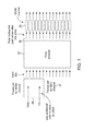
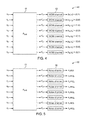
- FIG. 1 is a block diagram illustrating an example write process.
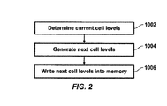
- FIG. 2 is a flow diagram that shows example operations performed by a device for encoding a data value in a WOM rewrite process.
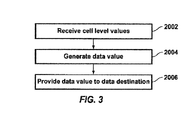
- FIG. 3 is a flow diagram that shows example operations performed by a device for decoding a cell charge level value in a WOM read process.
- FIG. 4 is a block diagram that shows an example device for encoding a cell charge level value in a WOM rewrite process.
- FIG. 5 is a block diagram that shows an example device for decoding a cell charge level value in a WOM read process.
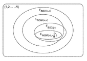
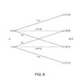
- FIG. 6 illustrates an example WOM channel WOM ( ⁇ , ⁇ ).
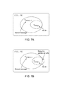
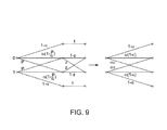
- FIG. 7 illustrates examples of: (a) Nested code for F BSC(p) ⁇ F WOM( ⁇ , ⁇ ) , (b) General code.
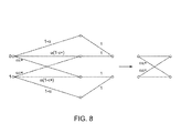
- FIG. 8 illustrates an example of: Degrading the channel WOM( ⁇ , ⁇ *) to BSC( ⁇ *).
- the two channels on the left and on the right may be equivalent.
- FIG. illustrates an example of: Degrading channel
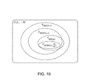
- FIG. 10 illustrates an example of: The frozen sets for channels BSC(p), WOM( ⁇ , ⁇ ),
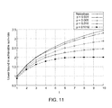
- FIG. 11 is a graph illustrating an example of: Lower bound to achievable sum-rates for different error probability p.
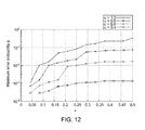
- FIG. 12 is a graph illustrating an example of: The maximum value of p found for which F BSC(p) ⁇ F WOM( ⁇ , ⁇ ).
- FIG. 14 is an illustration of an example memory device.
- FIG. 15 is a block diagram of an example computing device for communicating or otherwise operating with a memory device such as depicted in FIG. 14 .
- FIG. 16 is a block diagram that illustrates an example data flow in a system that operates according to aspects discussed herein.
- This disclosure is generally drawn, inter alia, to methods, apparatus, systems, devices, and computer program products related to joint rewriting and error correction in write-once memories.
- both rewriting and error correction are technologies that may be used for non-volatile memories, such as flash memories.
- This disclosure presents a coding scheme that combines rewriting and error correction for the write-once memory model.
- code construction is based on polar codes, and supports any number of rewrites and corrects a substantial number of errors.
- the code may be analyzed for a binary symmetric channel. The results can be extended to multi-level cells and more general noise models.
- the code construction scheme may support any number of rewrites and can correct a substantial number of errors.
- a memory may have N binary cells, where every cell has two charge levels: 0 and 1.
- the cell-programming method can only change a cell from 0 to 1, but not from 1 to 0.
- noise can change a cell in both directions: from 0 to 1, and from 1 to 0.
- the coding for the cell programming has two functions: (1) Rewrite data, which means to store new data that replace old data, and (2) Correct errors.
- a coding method may support t writes, where each write is also called a rewrite, and where t is an integer parameter greater than or equal to two.
- each of the writes may use substantially the same process.
- (s 1 , s 2 , . . . , sN) be a binary vector that represent the levels of the N binary cells before a write.
- (s′ 1 , s′ 2 , . . . , s′N) be a binary vector that represent cell levels of the N binary cells after this write.
- (b 1 , b 2 , . . . , bM) be a binary vector that represents the data to be written, where the data has M bits. Note the following constraints or conditions:
- the method may have the following inputs:
- the method computes the output (s′ 1 , s′ 2 , . . . , s′N), and programs the cells to the new levels with the following constraints:
- FIG. 1 is a block diagram illustrating an example write process in accordance with some embodiments.
- the write process of FIG. 1 includes error correction, for example, as described above.
- Data to be stored in the memory is included with the frozen set for WOM channel 26 , and is provided to the polar encoder 27 .
- the polar encoder 27 generates a polar codeword 28 , which is provided to a set of WOM channel device 29 .
- the WOM channel devices 29 determine cell levels to be written into the WOM.
- Data to be stored in the memory is included with the frozen set for WOM channel 26 , and data of the frozen set for WOM channel 26 is provided to the polar encoder 27 .
- additional data 31 is provided to the polar encoder 27 .
- the additional data 31 is a frozen set for a binary symmetric channel (BSC) channel.
- the polar encoder 27 generates the polar codeword 28 based on the data of the frozen set for WOM channel 26 and the additional data 31 of the frozen set for the BSC channel.
- the additional data 31 allows for the polar encoder 27 to generate a polar codeword 28 which includes data for error correction.
- the poplar encoder 27 generates the polar codeword 28 according to embodiments and example features of encoding schemes discussed in further detail below. As discussed below, the encoding schemes allow for the WOM to be written with error correction.
- the polar codeword 28 is provided to a set of WOM channel devices 29 , which determine cell levels to be written into the WOM.
- the WOM channel devices 29 determine the cell levels such that the new state of the WOM includes the data of the frozen set and such that the only cell level changes in the WOM are from the 0 state to the 1 state. Embodiments of WOM channel devices are described below in further detail.
- FIG. 2 is a flow diagram that shows example operations of a method that may be performed by a device for encoding a data value to be encoded into a codeword for rewriting the WOM in accordance with some embodiments.
- the device may comprise an external data storage device such as a flash memory device that receives data from a host device, such as a computer, and stores the data in accordance with error correction encoding schemes discussed below.
- the device may comprise an encoder for the purpose of processing data values and producing corresponding codewords.
- the method of FIG. 2 may include one or more operations, functions, or actions as illustrated by one or more of blocks 1002 , 1004 , and/or 1006 .
- blocks 1002 , 1004 , and/or 1006 may be implemented using any suitable method.
- the blocks are illustrated in a sequential order, these blocks may also be performed in parallel, and/or in a different order than those described herein.
- the various blocks may be combined into fewer blocks, divided into additional blocks, and/or eliminated based upon the particular implementation. Additional blocks may be provided that represent other operations, functions, or actions.
- Block 1002 determines current cell levels.
- Block 1002 may be followed by block 1004 “generate next cell levels,” and block 1004 may be followed by block 1006 “write next cell levels into memory.”
- current cell charge levels are determined.
- writing data into memory causes cell levels to change unidirectionally, for example, 0 to 1, but not 1 to 0. Accordingly, to determine which memory cells to change from 0 to 1, the current cell levels are determined.
- next cell charge levels are generated based on the data to be written and on the current cell levels. Examples of techniques for determining next cell levels are discussed in further detail below.
- the next cell charge levels are written into the memory.
- the next cell levels may be stored into memory cells of a data device, or maybe provided to a memory of a host device, or may be transmitted to an external destination.
- the rewriting method enable new data to be stored in cells (to replace old data) two or more times without decreasing cell levels.
- an error correction method enables the most recently written data to be recovered even though noise may have changed the levels of some of the cells.
- the new cell-level vector (s′ 1 , . . . , s′N) represents the new data (b 1 , b 2 , . . . , bM), according to the mapping specified by the method. Accordingly, given the new cell levels (s′ 1 , . . . , s′N), the decoding algorithm can uniquely determine the value of the new data (b 1 , . . . , bM).)
- FC contains at least one element. That is,
- At least one element of ⁇ 1, 2, . . . , N ⁇ is neither in FWOM nor in FC. That is,
- FC is a subset of FWOM. That is, FC ⁇ FWOM.
- the method may use a binary vector (g 1 , g 2 , : : : , gN) called a dither, whose value is known to the system.
- the value of the dither can be the same or different for each of the rewrites.
- Two other binary vectors (v 1 , v 2 , . . . , vN) and (v′ 1 , v′ 2 , . . . , v′N) may be determined as follows:
- ⁇ is the exclusive-OR operation.
- a ⁇ 1 N ⁇ N be the inverse of the matrix A N ⁇ N
- the vector (u 1 , u 2 , . . . , uN) may have the following properties:
- i ⁇ F C ⁇ is a constant (such as all 0s or any other fixed value) known to the system.
- the method may use the following 1 st probabilistic model to describe the relationship between cell levels (s 1 , . . . , sN) and (s′ 1 , . . . s′N).
- the method may use the new cell levels (s′ 1 , . . . , s′N) as the vector that maximizes or otherwise increases the value Pr ⁇ (s′ 1 , . . . , s′N)
- the method may choose the new cell levels (s′ 1 , . . . , s′N) as the vector that maximizes or otherwise increases the value Pr ⁇ (s 1 , . . . , sN)
- the method may use the following 2 nd probabilistic model to describe the relationship between vectors (v′ 1 , . . . , v′N) and ((s 1 ,v 1 ), . . . , (sn,vn)).
- I 1, . . . , N.
- the method may choose the new cell levels (s′ 1 , . . . , s′N) as the vector that maximizes or otherwise increases the value Pr ⁇ (s′ 1 , . . . , s′N)
- the method may choose the new cell levels (s′ 1 , . . . , s′N) as the vector that maximizes or otherwise increases the value Pr ⁇ (s 1 , . . . , sN)
- N the method may compute the following:
- the dither may be a pseudo-random number, which can be generated by a pseudo-random-number generator using a seed number as input.
- the seed number may be stored in the system.
- the method may compute the following:
- the matrix A N ⁇ N may be the generating matrix of a polar code
- FWOM may be contained in the frozen set of the polar code corresponding to the channel described by the transition 2 nd probabilistic model, where the channel has v′i as the channel input and (si, vi) as the channel output.
- FWOM may be determined as follows:
- 1) computed as discussed below.
- ⁇ R be a real number parameter greater than zero.
- F WOM ⁇ j 1 , j 2 , . .
- j N( ⁇ H( ⁇ ) ⁇ R) ⁇ be a subset of ⁇ 1, 2, . . . , N ⁇ with cardinality N(( ⁇ H( ⁇ ) ⁇ R), such that all values in ⁇ FER(W N i )
- the matrix A N ⁇ N may be the generating matrix of a polar code.
- noise may appear in the cells and change the cell levels to (c 1 , c 2 , . . . , CM), where ci is a bit that is not necessarily equal to s′i.
- the error-correction method takes the noisy cell levels (c 1 , c 2 , . . . , CM) as input, and outputs the stored data (b 1 , b 2 , . . . , bM).
- FIG. 3 is a flow diagram that shows example operations of a method performed by a device for decoding cell level values received from the WOM to generate a data value as part of a read operation, in accordance with some embodiments.
- the device may comprise an external data storage device such as a flash memory device that receives data from a host device, such as a computer, and stores the data in accordance with an error correction encoding and decoding scheme schemes discussed below.
- the device may comprise a decoder for the purpose of processing cell level values and producing corresponding data values.
- the method of FIG. 3 may include one or more operations, functions, or actions as illustrated by one or more of blocks 2002 , 2004 , and/or 2006 . Although the blocks are illustrated in a sequential order, these blocks may also be performed in parallel, and/or in a different order than those described herein. Also, the various blocks may be combined into fewer blocks, divided into additional blocks, and/or eliminated based upon the particular implementation. Additional blocks may be provided that represent other operations, functions, or actions.
- Block 2002 may begin in block 2002 “receive cell level values.”
- Block 2002 may be followed by block 2004 “generate data value,” and block 2004 may be followed by block 2006 “provide data value to data destination.”
- a set of cell level values to be decoded is retrieved from the WOM.
- the set of values is decoded to generate the corresponding data value. Examples of techniques for decoding are discussed in further detail below.
- the data value is provided to a data destination, such as a host computer.
- the data value may be transmitted by a transmitter to the data destination.
- the decoding or error correction function may use a binary vector (u′ 1 , . . . , 1 ′N) and has the following properties:
- the probability may be determined by the errors' probabilistic characteristic. Accordingly, for every i ⁇ FWOM ⁇ FC a data bit bj is recovered as u′i, where bj was assigned to ui for the most recent rewrite.
- FC contains at least one element. That is,
- At least one element of ⁇ 1, 2, . . . , N ⁇ is neither in FWOM nor in FC. That is,
- FC is a subset of FWOM. That is, FC ⁇ FWOM.
- the errors in the cells may have the following distribution:
- Pr ⁇ c i 0
- s′ i 0 ⁇ Pr ⁇ 0
- 0 ⁇ 1 ⁇ p 0
- Pr ⁇ c i 1
- s′ i 0 ⁇ Pr ⁇ 1
- 0 ⁇ p 0
- Pr ⁇ c i 0
- s′ i 1 ⁇ Pr ⁇ 0
- 1 ⁇ p 1
- Pr ⁇ c i 1
- s′ i 1 ⁇ Pr ⁇ 1
- 1 ⁇ 1 ⁇ p 1 .
- binary vector ((u′ 1 , . . . , 1 ′N) may have the following properties:
- the matrix A N ⁇ N may be the generating matrix of a polar code, and p is a real number parameter between zero and one.
- the method may correct errors and may recover the data values (b 1 , b 2 , . . . , bM) as follows:
- the most likely element in the list may then be chosen as the recovered value for (u 1 , . . . , uN).
- the stored data (b 1 , . . . , bM) may itself be an error-correcting code C and therefore may contain redundancy.
- the decoding algorithm, in 1 may be further specified as follows:
- the method checks if its value assignment to (u i
- the decoding algorithm may be based on a belief-propagation decoding algorithm for polar error-correcting codes.
- G ⁇ ⁇ 2 ( 1 0 1 1 )
- a N ⁇ N G 2 ⁇ m be the m-th Kronecker product of G 2 .
- recovering the value action discussed above may further include the following:
- i ⁇ F WOM ⁇ F C ⁇ be the recovered value for the data (b 1 , . . . , b M ), where the mapping from the bits in ⁇ u i
- the method may be a list-decoding algorithm further specified as follows:
- L be a positive integer parameter that indicates the size of a list, where each element in the list is an assignment of value to (u 1 , u 2 , . . . ,ui ⁇ 1) before the value of ui is computed.
- the method may include the following:
- the stored data (b 1 , . . . , bM) may itself be an error-correcting code C and therefore may contain redundancy and the method may include:
- L be a positive integer parameter that indicates the size of a list, where each, element in the list is an assignment of value to (u 1 , u 2 , . . . , ui ⁇ 1) before the value of ui is computed.
- the method further includes the following:
- i ⁇ F WOM ⁇ F C ⁇ be the recovered value for the data (b i , . . . , b M ), where the mapping from the bit in ⁇ u i
- FC may be determined as follows:
- the target block error rate be B, a non-negative real-number parameter between 0 and 1.
- (j 1 , j 2 , . . . , jN) be a permutation of ⁇ 1, 2, . . . , N ⁇ such that the decoding error probability of the bit uj 1 is the greatest, the decoding error probability of the bit uj 2 is the second greatest, and so on, and the decoding error probability of the bit ujN is the smallest.
- be chosen as the smallest integer such that the summation of the decoding error probabilities of the bits u j
- FC ⁇ j 1 , j 2 , . . . j
- FC is not a subset of FWOM. That is, FC ⁇ FWOM is not empty.
- the rewriting or encoding methods described above are modified to include storing the value of the bits ⁇ u i
- the error correction of decoding methods described above are modified to include recovering the value of the bits in ⁇ u i
- the error correction or decoding method described above may be such that the value of the bits in ⁇ u i
- FCj denotes the set FC for the j-th rewrite.
- FWOMj denotes the set FWOM for the j-th rewrite, and N additional additional cells are used for a code that supports t rewrites and error-correction processes.
- M
- bits are stored in the j-th rewrite.
- the code can be any code described herein.
- M
- bits are stored in the j-th rewrite, and methods of decoding discussed above may be modified such that the value of the bits in ⁇ u i
- methods of decoding discussed above may be modified such that the value of the bits in ⁇ u i
- the WOM cells are binary. In alternative or additional embodiments, every cell has q-levels: level 0, level 1, . . . , and level q-1,
- methods for rewriting and error-correction or encoding may use the cells in the following level-by-level approach:
- the methods may first use level 0 and level 1 and apply the previously described features for binary cells;
- the methods may then use level 1 and level 2 (as if they were level 0 and level 1) and apply the previously described features for binary cells;
- the methods may then use level 2 and level 3 (as if they were level 0 and level 1) and apply the previously described features for binary cells;
- the above process(es) may continue, until finally, the methods may use level q-2 and level q-1 (as if they were level 0 and level 1) and apply the previously described features for binary cells.
- methods for rewriting and error correction or encoding may be modified such that each ui, si, gi, vi, s′i or v′i takes its value from the set ⁇ 0,1, . . . , q-1 ⁇ , and the exclusive-OR operation may be generalized to the modular-q summation.
- our method has the following inputs: (1) The current cell levels (s 1 , s 2 , . . . , s N ), and (2) the new data to store (1, b 2 , . . . b M ). It then computes the output (s′ 1 , s′ 2 , . . . , s′ N ), and programs the cells to those new levels.
- FIG. 5 illustrates an embodiment of a decoder.
- the noise channels 52 are each a binary-symmetric channel with error probability p.
- Section II includes a basic model and notations.
- Section III includes an embodiment of code construction.
- Section IV includes embodiments of code.
- Section V includes embodiments of code extensions.
- Section VI includes an analysis of actual sum-rates achieved by a code embodiment.
- Section VII includes further example embodiments.
- Section VIII includes concluding remarks.
- a sequence of t messages M 1 , M 2 , . . . , M t may be written into the WOM cells, and when M i is written, the value of the previous messages need not be remembered.
- Let M j denote the number of bits in the message M j , and let M j ⁇ 0,1 ⁇ M j .
- the cells be all at level 0 before the first write happens.
- Noise may be considered to be a BSC with error probability p, denoted by BSC(p).
- BSC(p) error probability
- These errors may be hard errors, namely, they physically change the cell levels from 0 to 1 or from 1 to 0.
- errors can be caused by read/write disturbs, interference and charge leakage, for example, and may be quite common.
- a code for rewriting and error correction may comprise of t encoding functions E 1 , E 2 , . . . , E t and t decoding functions D 1 , D 2 , . . . , D t .
- s′ i,j ⁇ s i,j .
- c i,j ⁇ 0,1 ⁇ denote the level of the i-th cell at any time after the j-th write and before the (j+1)-th write, when reading of the message M j can happen.
- the error c i,j ⁇ s′ i,j ⁇ 0,1 ⁇ is the error in the i-th cell caused by the noise channel BSC(p).
- ⁇ is an XOR function.
- R j is called the sum-rate of the code.
- a polar code is a linear block error correcting code proposed by Arkan, See, e.g. E. Arkan, “Channel polarization: A method for constructing capacity-achieving codes for symmetric binary-input memoryless channels,” IEEE Trans. Inf. Theor ., vol. 55, no. 7, pp. 3051-3073, July 2009. It is the first known code with an explicit construction that provably achieves the channel capacity of symmetric binary-input discrete memoryless channels (B-DMC).
- G 2 ( 1 0 1 1 )
- G 2 ⁇ m is the m-th Kronecker product of G 2 .
- the N codeword bits (x 1 , x 2 , . . . , x N ) are transmitted through N independent copies of a B-DMC.
- N transformed binary input channels ⁇ W N (1) , W N (2) , . . . , W N (N) ⁇ can be synthesized for u 1 , u 2 , . . . , u N , respectively.
- the channels are polarized such that for large N, the fraction of indices i for which I(W N (t) ) is nearly 1 approaches the capacity of the B-DMC, while the values of I(W N (i) ) for the remaining indices i are nearly 0.
- the latter set of indices are called the frozen set.
- the u i ′s with i in the frozen set take fixed values, and the other u i ′s are used as information bits.
- a successive cancellation (SC) decoding algorithm achieves diminishing block error probability as N increases.
- Polar code can also be used for optimal lossy source coding, which has various applications. See, e.g. S. Korada and R. Urbanke, “Polar codes are optimal for lossy source coding,” IEEE Trans. Inf. Theor ., vol. 56, no. 4, pp. 1751-1768, April 2010. In particular the idea may be used to build capacity achieving WOM codes. See, e.g., D. Burshtein and A. Strugatski, “Polar write once memory codes,” in Proc. IEEE international Symposium on Information Theory, July 2012, pp., 1972-1976.
- the presented code analysis uses the concept of upgrading and degrading channels, defined based on frozen sets.
- a channel W′: X ⁇ Z is called “degraded with respect to a channel W: X ⁇ Y” if an equivalent channel of W′ can be constructed by concatenating W with an additional channel Q: Y ⁇ Z, where the inputs of Q are linked with the outputs of W.
- x ) ⁇ y ⁇ y W ( y
- W′ ⁇ W It may be denoted as W′ ⁇ W. Equivalently, the channel W is called “an upgrade with respect to W′”, denoted by W ⁇ W′.
- F BSC(p) ⁇ F WOM( ⁇ , ⁇ ) .
- the code has a nice nested structure: for any message M ⁇ 0,1 ⁇ M , the set of cell values V M ⁇ 0,1 ⁇ N that represent the message M is a linear subspace of a linear error correcting code (ECC) for the noise channel BSC(p), and ⁇ V M
- ECC linear error correcting code
- u F WOM ⁇ ( ⁇ , ⁇ ) - F BSC ⁇ ( p ) ⁇ ⁇ ⁇ ⁇ u i
- i ⁇ F WOM ⁇ ( ⁇ , ⁇ ) - F BSC ⁇ ( p ) ⁇ are all the bits u i in the frozen set F WOM( ⁇ , ⁇ ) but not
- F BSC ⁇ ( p ) , u F BSC ⁇ ( p ) ⁇ ⁇ ⁇ ⁇ u i
- i ⁇ F BSC ⁇ ( p ) ⁇ are all the bits u i in F BSC(p) , and G 2 ⁇ m is the m-th Kronecker product of
- the decoder may be configured to operate the same way as a polar error correcting code.
- the decoding operation of one embodiment is presented as Algorithm 2.
- t for the j-th write, replace ⁇ , ⁇ , s, s′, v, v′, M, M, E, D, c, ⁇ circumflex over (M) ⁇ , ⁇ circumflex over (v) ⁇ , by ⁇ j ⁇ 1 , ⁇ j , s j , s′ j , v j , v′ j , M j , M j , E j , D j , c j , ⁇ circumflex over (M) ⁇ j , ⁇ circumflex over (v) ⁇ j , respectively, and apply the above encoder and decoder.
- Improving the code may include choosing other values for ⁇ 1 , ⁇ 2 , . . . , ⁇ t that maximize or otherwise increases the sum-rate.
- the encoder in Algorithm 1 may be revised as follows.
- the bits are then stored in u F BSC(p)- F WOM( ⁇ , ⁇ ) using N additional,j cells (for the j-th write).
- This implementation is illustrated in FIG. 7( b ) .
- the bits in u F BSC(p)- F WOM( ⁇ , ⁇ ) are stored using just an error correcting code designed for the noise channel BSC(p).
- the bits can be stored using an error-correcting WOM code, such as the one presented above, for higher rates.
- the decoder in Algorithm 2 may be revised as follows. First recover the bits in u F BSC(p)-F WOM( ⁇ , ⁇ ) using the decoding algorithm of the ECC for the N additional,j additional cells. Then carry out Algorithm 2, except that the bits in F BSC(p) -F WOM( ⁇ , ⁇ ) are known to the decoder as the above recovered values instead of 0s.
- the encoder in Algorithm 1 works similarly to the WOM code encoder in D. Burshtein and A. Strugatski, “Polar write once memory codes.” In Proc. IEEE International Symposium on Information Theory, July 2012, pp. 1972-1976, with an exception that the bits in F WOM( ⁇ , ⁇ ) are not all occupied by the message M, instead, the bits in its subset F WOM( ⁇ , ⁇ ) ⁇ F BSC(p) are set to be constant values: all 0s. Therefore, the encoder successfully rewrites data in the same way as the code in D. Burshtein and A. Sgresatski, “Polar write once memory codes,” in Proc. IEEE International Symposium on Information Theory, July 2012, pp. 1972-1976.
- the decoder in Algorithm 2 recovers the cell values from noise in the same way as the standard polar ECC. Then, the stored message M is extracted from it.
- the pseudo-random dither g has independent and uniformly distributed elements, and so when the noise channel for s is BSC(p), the corresponding noise channel for v is also BSC(p).
- Lemma 2 The meaning of Lemma 2 is illustrated in FIG. 10 .
- N additional , j NH ⁇ ( p ) ⁇ ( 1 - x j ) 1 - H ⁇ ( p )
- ⁇ i 1 2 + t - i .
- noise a binary erasure channel (BEC) with erasure probability p, denoted by BEC(p).
- BEC binary erasure channel
- p erasure probability
- An erasure represents a noisy cell level between 0 and 1. Erasures may be handled as follows: before a rewrite, all the erased cell levels are increased to 1, and then rewriting is performed as before.
- the code can also be extended to multi-level cells (MLC), by using q-ary polar codes.
- MLC multi-level cells
- example achievable rates of the error correcting WOM code are discussed, using polar codes of finite lengths.
- the noise channel is BSC(p)
- search is performed for parameters ⁇ 1 , ⁇ 2 , . . . , ⁇ t that achieve high sum-rate for rewriting.
- the code can have a nested structure is also discussed. This simplifies the code construction.
- the first consideration is when BSC(p) satisfies the condition F BSC(p) ⁇ F WOM( ⁇ , ⁇ ) , which leads to a particular nested code structure.
- N 8192.
- the polar codes be constructed using the method(s) described herein. To obtain the frozen sets, let
- Example results are shown in FIG. 12 .
- the x-axis is ⁇
- the y-axis is the maximum value of p that satisfies F BSC(p) ⁇ F WOM( ⁇ , ⁇ ) .
- the maximum value of p increases with both ⁇ and ⁇ and has nontrivial values (namely, p is comparable to or higher than the typical error probabilities in memories).
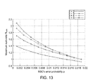
- Results for t-write error-correcting WOM codes—for t 2,3,4,5—are shown in FIG. 13 .
- the x-axis is p and the y-axis is the maximum sum-rate found in the algorithmic search. Accordingly, the achievable sum-rate increases with the number of rewrites t.
- the lower bound to sum-rate R sum is discussed with reference to FIG. 10 . of Note that one embodiment may actually be higher than the rates found in other embodiments. This is because the lower bound is for N ⁇ , while the codes in the other embodiments may be still short so far and may consider the rate loss ⁇ R. Better rates can be provided as the code length is increased and as the search algorithm is further improved due to the results indicated by the lower bound.
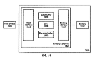
- FIG. 14 is an illustration of one embodiment of a data device constructed/configured so as to perform the methods and operations discussed herein.
- FIG. 14 shows a memory 1602 that is accessed by a memory controller 1604 that communicates with a host device 1606 .
- the memory 1602 is used for storing data that is represented in accordance with an encoding and decoding scheme discussed herein.
- the memory may be implemented, for example, as a Flash memory having multilevel cells.
- the memory 1602 and memory controller 1604 together at least partly form a data storage device 1608 that may be external to the host device or may be integrated with the host device into a single component or system.
- the data storage device 1608 may comprise a Flash memory device (often referred to as a “thumb drive”) that communicates with a host computer 1606 via a USB connection, or the data storage device may comprise a solid state drive (SSD) that stores data for a host computer system.
- the data storage device may integrated with a suitable host device to comprise a single system or component with memory employing an embodiment of a encoding and decoding scheme as discussed herein, such as a smart phone, network router, MP3 player, or the like.
- the memory controller 1604 operates under control of a microcontroller 1610 , which manages communications with the memory 1602 via a write device, such as memory interface 1612 and manages communications with the host device via a host interface 1614 .
- the memory controller supervises data transfers from the host 1606 to the memory 1602 and from the memory 1602 to the host 1606 .
- the memory controller 1604 also includes a data buffer 1616 in which data values may be temporarily stored for transmission over the data channel controller 1617 between the memory 1602 and the host 1606 .
- They memory controller also includes an Error Correcting code (ECC) block 1618 in which data for the ECC is maintained.
- ECC Error Correcting code
- the ECC block 1618 may comprise data and program code to perform error correction operations for a an embodiment of a encoding and decoding scheme as discussed herein. Some embodiments of such error correction operations are described, for example, in U.S. Patent Application entitled “Error Correcting Codes for Rank Modulation” by Anxiao Jiang et al. filed Nov. 20, 2008, and incorporated herein by reference.
- the ECC block 1618 may contain parameters for the error correction code to be used for the memory 1602 , such as programmed operations for translating between received symbols and error-corrected symbols, or the ECC block may contain lookup tables for codewords or other data, or the like.
- the memory controller 1604 of one embodiment may perform the operations described above for decoding data and for encoding data.
- the operations described above for operating a data storage device, for reading data from a device, for programming a data storage device, and encoding and decoding, can be carried out by the operations discussed above which can be performed by the microcontroller 1610 and associated components of the data storage device 1608 .
- the processing components such as the controller 1604 and microcontroller 1610 to perform the various operations described herein may be implemented in some embodiments in the form of control logic in software (or other computer-readable instruction stored on a non-transitory computer-readable storage medium and executable by one or more processors) or hardware or a combination of both, and may comprise the processor(s) that execute software program instructions from program memory, or as firmware, or the like.
- the host device 1606 may comprise a computer apparatus. A computer apparatus also may carry out the operations depicted in the various figures herein or otherwise described above.
- FIG. 15 is a block diagram illustrating an example computing device 900 that includes elements that pertain to the encoding and decoding operations, error correction operation, memory cells, etc. discussed herein in connection with a read and write data from a memory.
- computing device 900 typically includes one or more processors 910 and system memory 920 .
- a memory bus 930 can be used for communicating between the processor 910 and the system memory 920 .
- processor 910 can be of any type including but not limited to a microprocessor ( ⁇ P), a microcontroller ( ⁇ C), a digital signal processor (DSP), or any combination thereof.
- Processor 910 can include one more levels of caching, such as a level one cache 911 and a level two cache 912 , a processor core 913 , and registers 914 .
- the processor core 913 can include an arithmetic logic unit (ALU), a floating point unit (FPU), a digital signal processing core (DSP Core), or any combination thereof.
- a memory controller 915 can also be used with the processor 910 , or in some implementations the memory controller 915 can be an internal part of the processor 910 .
- system memory 920 can be of any type including but not limited to volatile memory (such as RAM), non-volatile memory (such as ROM, flash memory, etc.) or any combination thereof.
- System memory 920 typically includes an operating system 921 , one or more applications 922 , and program data 924 .
- Applications 922 include encoding and decoding algorithms 923 that is arranged to encode and decode, for example, program data 924 as discussed below.
- applications 922 can be arranged to operate with program data 924 on an operating system 921 .
- This described basic configuration is illustrated in FIG. 9 by those components within dashed line 901 .
- the applications(s) 922 can include one or more algorithms 923 having computer-readable instructions that are stored on a non-transitory (such as hardware) computer-readable medium and that are executable by one or more processors (such as the processor 910 ) to perform the joint rewriting and error correction of a WOM as described herein.
- the program data 924 of one embodiment may include various data 925 , such as the data written to or read from the WOM, the data for the various equations/variable/vectors/algorithms/etc. described above, or other data.
- Computing device 900 can have additional features or functionality, and additional interfaces to facilitate communications between the basic configuration 901 and any required devices and interfaces.
- a bus/interface controller 940 can be used to facilitate communications in accordance with the present disclosure between the basic configuration 901 and one or more data storage devices 950 via a storage interface bus 941 .
- the data storage devices 950 can be removable storage devices 951 , non-removable storage devices 952 , or a combination thereof. Examples of removable storage and non-removable storage devices include magnetic disk devices such as flexible disk drives and hard-disk drives (HHDs), optical disk drives such as compact disk (CD) drives or digital versatile disk (DVD) drives, solid state drives (SSDs), and tape drives to name a few.
- Example computer storage media can include volatile and nonvolatile, removable and non-removable media implemented in any method or technology for storage of information, such as computer readable instructions, data structures, program modules, or other data.
- Computer storage media includes, but is not limited to, RAM, ROM, EEPROM, flash memory or other memory technology, CD-ROM, digital versatile disks (DVDs) or other optical storage, magnetic cassettes, magnetic tape, magnetic disk storage or other magnetic storage devices, or any other medium which can be used to store the desired information and which can be accessed by computing device 900 . Any such computer storage media can be part of device 900 .
- Computing device 900 can also include an interface bus 942 for facilitating communication from various interface devices (e.g., output interfaces, peripheral interfaces, and communication interfaces) to the basic configuration 901 via the bus/interface controller 940 .
- Example output devices 960 include a graphics processing unit 961 and an audio processing unit 962 , which can be configured to communicate to various external devices such as a display or speakers via one or more A/V ports 963 .
- Example peripheral interfaces 970 include a serial Interface controller 971 or a parallel interlace controller 972 , which can be configured to communicate with external devices such as input devices (e.g., keyboard, mouse, pen, voice input device, touch input device, etc.) or other peripheral devices (e.g.
- An example communication device 980 includes a network controller 981 , which can be arranged to facilitate communications with one or more other computing devices 990 over a network communication via one or more communication ports 982 .
- the communication connection is one example of a communication media.
- Communication media may typically be embodied by computer readable instructions, data structures, program modules, or other data in a modulated data signal, such as a carrier wave or other transport mechanism, and includes any information delivery media.
- a “modulated data signal” can be a signal that has one or more of its characteristics set or changed in such a manner as to encode information in the signal.
- communication media can include wired media such as a wired network or direct-wired connection, and wireless media such as acoustic, radio frequency (RF), infrared (IR) and other wireless media.
- RF radio frequency
- IR infrared
- computer readable media can include both storage media and communication media.
- Computing device 900 can be implemented as a portion of a small-form factor portable (or mobile) electronic device such as a cell phone, a personal data assistant (PDA), a personal media player device, a wireless web-watch device, a personal headset device, an application specific device, or a hybrid device that include any of the above functions.
- a small-form factor portable (or mobile) electronic device such as a cell phone, a personal data assistant (PDA), a personal media player device, a wireless web-watch device, a personal headset device, an application specific device, or a hybrid device that include any of the above functions.
- PDA personal data assistant
- Computing device 900 can also be implemented as a personal computer including both laptop computer and non-laptop computer configurations.
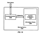
- FIG. 16 shows data flow in a memory device 1302 , such as data storage device 1608 discussed above with reference to FIG. 14 , that operates according to the error correction encoding schemes described herein.
- the memory device 1302 includes an encoder and decoder 1308 for encoding data values into codewords and decoding codewords into data values.
- the encoder and decoder 1308 encodes data values and provides codewords to the source/destination block 1310 , and decodes codewords from the source/destination and provides corresponding data values.
- the encoder and decoder 1308 includes interfaces through which the encoder and decoder 1308 receives and provides the data values and the information values (codewords). For the sake of brevity, further details of such interfaces are not provided herein. While represented as a single block/unit that is labeled as 1308 in FIG. 16 , the encoder and decoder can comprise discrete and separate blocks/units in other embodiments.
- the information values 1306 comprise a physical representation of the data values and codewords.
- the information values 1306 may represent charge levels of memory cells, such that multiple cells are configured to operate as virtual cell in which charge levels of the cells determine a representation of the data values with error correction. Data values are received and encoded to represent the data values with error correction and charge levels of cells are adjusted accordingly, and codewords are determined according to cell charge levels, from which a corresponding data value is determined.
- the information values 1306 may represent features of a transmitted signal, such as signal frequency, magnitude, or duration, such that the cells or bins are defined by the signal features and represent a data value having error correction. For example, frequency changes over time can determine a data value having error correction.
- Other schemes for physical representation of the cells are possible in view of the description herein.
- the source/destination 1310 comprises memory cells in which n memory cells provide n cell values whose charge levels define data values having error correction.
- the memory cells receive an encoded codeword and comprise a destination, and for reading a code word, the memory cells provide a codeword for decoding and comprise a source.
- the source/destination 1310 may comprise a write device, such as a transmitter/receiver that processes a signal with signal features such as frequency, magnitude, or duration that define cells or bins such that the signal features determine a data value having error correction.
- signal components comprising signal frequency, magnitude, or duration may be controlled and modulated by the transmitter such that data values having error correction are represented.
- the source/destination 1310 receives a codeword from the controller 1304 , the source/destination comprises a transmitter of the device 1302 for sending an encoded signal.
- the source/destination provides a codeword to the controller 1304 from a received signal, the source/destination comprises a receiver of the device for receiving an encoded signal.
- Signal components of the transmitted signal can be suitable modulated to define data values having error correction, in view of the description herein.
- control logic in software or hardware or a combination of both.
- the control logic may be stored in an information storage medium as a plurality of instructions adapted to direct an information-processing device to perform the operations discussed herein. Based on the disclosure and teachings provided herein, other ways and/or methods to implement the discussed features are possible.
- codewords may be received from a source over an information channel according to a memory writing scheme and are decoded into their corresponding data values and provided to a destination, such as a memory or a processor, and data values for storage or transmission are received from a source over an information channel and are encoded according to the memory writing scheme.
- the coding scheme can be further extended to multi-level cells (MLC).
- MLC multi-level cells
- multilevel cell memories can be written level by level.
- aspects of the coding scheme described above may be used for writing multilevel cell memories using a multilevel polar code.
- This application presents a code construction for error-correcting WOM codes.
- the embodiment(s) described herein supports any number of rewrites and can correct a substantial number of errors.
- construction may be based on polar coding to achieve improved performance for both rewriting and error correction.
- a range includes each individual member.
- a group having 1-3 cells refers to groups having 1, 2, or 3 cells.
- a group having 1-5 cells refers to groups having 1, 2, 3, 4, and 5 cells, and so forth.
Landscapes
- Engineering & Computer Science (AREA)
- Theoretical Computer Science (AREA)
- Physics & Mathematics (AREA)
- General Engineering & Computer Science (AREA)
- General Physics & Mathematics (AREA)
- Human Computer Interaction (AREA)
- Quality & Reliability (AREA)
- Probability & Statistics with Applications (AREA)
- Computer Security & Cryptography (AREA)
- Read Only Memory (AREA)
- Error Detection And Correction (AREA)
Abstract
Description
to WOM(α,ε). Here
The two channels on the left and on the right may be equivalent.
and BSC(αε). Here p≤αε.
-
- 1) For i=1, 2, . . . , N, s′i is greater than or equal to si. This is because the cell-programming method increases a cell's level, but may not decrease it.
- 2) M is an integer parameter known to the system. Its value can be the same or different for the writes.
- 3) The cell levels (s1, s2, . . . , sN) can be different from the cell levels right after the previous rewrite, because noise may have changed the cell levels since the previous rewrite.
-
- (1) The current cell levels (s1, s2, . . . , sN), and
- (2) The new data to store (b1, b2, . . . , bM).
-
- 1) For i=1, 2, . . . , N, s′i is greater than or equal to si.
- 2) The new cell levels (s′1, s′2, . . . , siN) represents the new data (b1, b2, . . . , bM), according to the mapping specified by the method.
and let ϵϵ[0, 1] be a real-number parameter whose value is known to the system. For i=1, . . . , N,
- Pr((si, νi)=(1,0)|ν′i=0)=1−α, Pr((si, νi)=(0,0)|ν′i=0)=α(1−ϵ), Pr((si, νi)=(0,1)|ν′i=0)=αϵ, Pr((si, νi)=(1,1)|ν′t=0)=0,
- Pr((si, νi)=(1,0)|ν′t=1)=0, Pr((si, νi)=(0,0)|ν′i=1)=αϵ, Pr(si, νi)=(0,1)|νi=1=α(1−ϵ), Pr((si, νi)=(1,1)|ν′i=1)=1−α.
and let AN×N=G2 ⊕m be the m-th Krobecker product of G2.
-
- Step 1: Let y=(y1, y2 . . . , yN)=((s1, ν1), (s2, ν2, . . . . , (sN, νN)) be a vector of N elements, where every element yi=(si, νi) is a pair of bits.
- Step 2: Let J=(j1, j2), . . . jM)=FWOM−FC where j1<j2< . . . <jm. Let uF
WOM−F C=(uj1, uj2, . . . , ujM). - For I=1, . . . , M, let uji=bt.
- Step 3: For every iϵFC, let ui=0.
- Step 4: Compute the values of WN i(y, (u1, u2, . . . , ui−1)|ui−1|ui=0) and WN i(y, (uj1, uj2, . . . , ui−1|ui=1) for i=1, 2, . . . , N as follows:
- Depending on the parity of i, the value of WN i is recursively evaluated through one of the formulae below (beginning with n=N/2):
with the base cases
W 1 1((1,0),(*)|0)=1−α
W 1 1((0,0),(*)|0)=α(1−ϵ)
W 1 1((0,1),(*)|0)=αϵ
W 1 1((1,1),(*)|0)=0
W 1 1((1,0),(*)|1)=0
W 1 1((0,0),(*)|1)=αϵ
W 1 1((0,1),(*)|1)=α(1−ϵ)
W 1 1((1,1),(*)|1)=1−α. (3)
-
- where (*) denotes an empty vector. The operator {circle around (l)} between two binary vectors denotes the element-wise exclusive-OR computation. The operator ⊖ between two bits denotes the binary exclusive-OR computation.
- Step 5: For i=1, 2, . . . , N, if i∉FWOM, then do the following:
- Step 5.1: Let LN i (y, (u1, u2, . . . , ui−1)) take the value
- WN i (y, (u1, u2, . . . , ui−1)|ui=0)/WN i(y, (u1, u2, . . . , ui−1)|ui=1).
- Step 5.2: Let ui take the
value 0 with probability
-
- and take the
value 1 probability
- and take the
-
- Step 6: Let (ν′1, ν′2, . . . , ν′N)=(u1, u2, . . . , uN) AN×N;
- Step 7: Let (s′1, s′2, . . . , s′N)=(ν′1⊕g1, ν′2⊕g2, . . . , ν′N⊕gN).
- Step 8: Check if s′1≥si for i=1, . . . , N. If yes, store the seed number used to generate the dither (g1, . . . , gN) in the system, and let (s′1, . . . , s′N) be the new cell levels; otherwise, use a new seed number to generate a new value for the dither (g1, . . . , gN), and return to
Step 1 to repeat the computation.
Where WN i(z|0) and WN i(z|1) computed as discussed below. In addition, let ΔR be a real number parameter greater than zero. Furthermore, let FWOM={j1, j2, . . . , jN(αH(ϵ)−ΔR)} be a subset of {1, 2, . . . , N} with cardinality N((αH(ϵ)−ΔR), such that all values in {FER(WN i)|iϵFWOM} are greater than or equal to each value in {FER(WN i)|iϵ{1, . . . , N}−FWOM}.
-
- The polar code's generating matrix is AN×N.
- The polar code encodes the user data (u1, . . . , uN) into the codeword (ν′1, . . . , ν′N) via the formula (ν′1, . . . , ν′N)=(u1, . . . , uN)AN×N.
- For i=1, . . . , N, the codeword bit ν′1 is transmitted through a binary-symmetric channel with transition probability p; and the output of that binary-symmetric channel is the noisy codeword bit ci.
- The frozen set of the polar code corresponding to the binary-symmetric channel is contained in FC; and when encoding user data into the codeword, the user-data bits in FC are fixed at known values (such as all 0's).
- The decoding algorithm considers (c1, . . . , cN) as the noisy codeword, and recovers the correct value of the original codeword (ν′1, . . . , ν′N).
-
- If iϵFC, let ui be the constant value that was assigned to it by the previous rewrite.
- If i∉FC, let ui take the value that maximizes the value of Pr{ui|c1, . . . , cN, u1, . . . , ui−1} assuming that each of ui+1, . . . , uN is equally likely to be 0 and 1.
- Let L be a positive integer parameter that indicates the size of a list, where each element in the list is an assignment of value to (u1, u2, . . . , ui−1) before the value of ui is computed. For i=1, . . . , N, the decoding algorithm computes the value of ui with the following:
and let AN×N=G2 ⊕m be the m-th Kronecker product of G2.
-
- Depending on the parity of i, the value of WN i is recursively evaluated through one of the formulae below (beginning with n=N/2):
-
- with the base cases
W 1 1((0),(.)|0)=1−p
W 1 1((1),(.)|0)=p
W 1 1((0),(.)|1)=p
W 1 1((1),(.)|1)=1−p (7)
where (.) denotes an empty vector. The operator ⊕ between two binary vectors denotes the element-wise exclusive-OR computation. The operator ⊕ between two bits denotes the binary exclusive-OR computation.
- with the base cases
-
- Depending on the parity of i, the value of WN i is recursively evaluated through one of the formulae below (beginning with n=N/2):
with the base cases
W 1 1((0),(.)|0)=1−p
W 1 1((1),(.)|0)=p
W 1 1((0),(.)|1)=p
W 1 1((1),(.)|1)=1−p (10)
where (.) denotes an empty vector. The operator ⊕ between two binary vectors denotes the element-wise exclusive-OR computation. The operator ⊕ between two bits denotes the binary exclusive-OR computation.
-
- If iϵFC, for each element in the list (which is an assignment of value to (u1, u2, . . . , ui−1), append it to the value assignment ui=0, and also append it to the value assignment ui=1, thus converting that element into two new elements in the list. If the list now contains more than L elements, keep only the L elements that are most likely in the list. The likelihood of an element in the list may be computed as WN i((y1, . . . . , yN), (u1, . . . , ui−1)|ui).
-
- Depending on the parity of i, the value of WN i is recursively evaluated through one of the formulae below (beginning with n=N/2):
with the base cases
W 1 1((0),(.)|0)=1−p
W 1 1((1),(.)|0)=p
W 1 1((0),(.)|1)=p
W 1 1((1),(.)|1)=1−p (13)
where (.) denotes an empty vector. The operator ⊕ between two binary vectors denotes the element-wise exclusive-OR computation. The operator ⊕ between two bits denotes the binary exclusive-OR computation.
-
- If iϵFC, let ui=0.
- If i∉FC, for each element in the list (which is an assignment of value to (u1, u2, . . . , ui−1), append it to the value assignment ui=0, and also append it to the value assignment ui=1, thus converting that element into two new elements in the list. If the list now contains more than L elements, keep only the L elements that are most likely in the list. The likelihood of an element in the list may be computed as WN i((y1, . . . , yN), (u1, . . . , ui−1)|ui).
-
- 1) As mentioned before, for i=1, 2, . . . , N, we have the constraint that is s′i≥si.
- 2) The new cell levels (s′1, s′2, . . . , s′N) represents the new data (b1, b2, . . . , bM), via the mapping specified by our method.
E j:{0,1}N×{0,1}M
changes the cell levels from sj=(s1,j, s2,j, . . . , sN,j) to s′j=(s′1,j, s′2,j, . . . , s′N,j) given the initial cell state sj and the message to store Mj. (Namely, Ej(sj, Mj)=s′j.) When the reading of Mj happens, the decoding function
D j:{0,1}N→{0,1}M
recovers the message Mj given the noisy cell state cj=(c1,j, c2,j, . . . cN,j). Namely, Dj(c1)=Mj.)
is called the rate of the j-th write. Rsum=Σj=1 t Rj is called the sum-rate of the code. When there is no noise, the maximum sum-rate of WOM code is known to be log2(t+1), however, for noisy WOM, the maximum sum-rate is still largely unknown.
and G2 ⊕m is the m-th Kronecker product of G2.) The N codeword bits (x1, x2, . . . , xN) are transmitted through N independent copies of a B-DMC. For decoding, N transformed binary input channels {WN (1), WN (2), . . . , WN (N)} can be synthesized for u1, u2, . . . , uN, respectively. The channels are polarized such that for large N, the fraction of indices i for which I(WN (t)) is nearly 1 approaches the capacity of the B-DMC, while the values of I(WN (i)) for the remaining indices i are nearly 0. The latter set of indices are called the frozen set. For error correction, the ui′s with i in the frozen set take fixed values, and the other ui′s are used as information bits. A successive cancellation (SC) decoding algorithm achieves diminishing block error probability as N increases.
W′(z|x)=Σyϵy W(y|x)Q(z|y)
are given parameters, with
representing the fraction of cells, at
representing the fraction of cells that are changed from
See, e.g. I. Tal and A. Vardy, “How to construct polar codes,” CoRR, vol. abs/1105.61.64,2011.
are all the bits ui in the frozen set FWOM(α,ε) but not
are all the bits ui in FBSC(p), and G2 ⊕m is the m-th Kronecker product of
| |
| y ← ((s1, v1), (s2, v2), . . . ,(sN, vN)). |
| Let uF |
| Let uF |
| for i from 1 to N do |
| if i ∉ FWOM(α,ε) then |
|
|
| (Comment: Here WN (i) (y, (u1, u2, . . . , ui−1)|ui = 0) |
| and WN (i) (y, (u1, u2, . . . , ui−1)|ui = 1) can be computed recursively |
| using formulae (22), (23) in E. Arikan, “Channel polarization: A method |
| for constructing capacity-achieving codes for symmetric binary-input |
| memoryless channels,” IEEE Trans. Inf. Theor., vol. 55, no. 7, |
| pp. 3051-3073, July 2009,). |
|
|
| Let v′ ← G2 ⊗m. |
| Let s′ ← v′ ⊕ g. |
| | ||
| View c ⊕ g as a noisy codeword, which is the output of a binary | ||
| symmetric channel BSC(p). | ||
| Decode c ⊕ g using the decoding algorithm of the polar error- | ||
| correcting code, where the bits in the frozen set FBSC(p) are set to | ||
| 0s. Let {circumflex over (v)} = ({circumflex over (v)}1, {circumflex over (v)}2, ..., {circumflex over (v)}N) be the recovered codeword. | ||
| Let {circumflex over (M)} ← ({circumflex over (v)}(G2 ⊗m)−1)F | ||
| of the vector {circumflex over (v)}(G2 ⊗m)−1 | ||
| whose indices are the set FWOM(α, | ||
As is clear from the polar error-correcting code, the encoding and the decoding algorithms may have time complexity O(NlogN).
And the sum-rate becomes
note that
Therefore
Therefore,
For j=1, 2, . . . , t, the number of bits written in the j-th rewrite is
and the number of additional cells used to store the bits in FBSC(p)−FWOM (αj−1−8j) is
(Σj=1 tαj−1 H(εj))−H(p)t.
The curve for p=0 is the optimal sum-rate for noiseless WOM code. The other four curves are the lower bounds for noisy WOM with p=0.001, p=0.005, p=0.010 and p=0.016, respectively, given by
because all the erased cell levels have been pushed to
Claims (25)
Priority Applications (1)
| Application Number | Priority Date | Filing Date | Title |
|---|---|---|---|
| US14/443,349 US9946475B2 (en) | 2013-01-24 | 2013-07-05 | Joint rewriting and error correction in write-once memories |
Applications Claiming Priority (3)
| Application Number | Priority Date | Filing Date | Title |
|---|---|---|---|
| US201361756324P | 2013-01-24 | 2013-01-24 | |
| US14/443,349 US9946475B2 (en) | 2013-01-24 | 2013-07-05 | Joint rewriting and error correction in write-once memories |
| PCT/US2013/049480 WO2014116301A1 (en) | 2013-01-24 | 2013-07-05 | Joint rewriting and error correction in write-once memories |
Publications (2)
| Publication Number | Publication Date |
|---|---|
| US20150293716A1 US20150293716A1 (en) | 2015-10-15 |
| US9946475B2 true US9946475B2 (en) | 2018-04-17 |
Family
ID=51227938
Family Applications (1)
| Application Number | Title | Priority Date | Filing Date |
|---|---|---|---|
| US14/443,349 Active 2033-11-21 US9946475B2 (en) | 2013-01-24 | 2013-07-05 | Joint rewriting and error correction in write-once memories |
Country Status (4)
| Country | Link |
|---|---|
| US (1) | US9946475B2 (en) |
| KR (1) | KR101710025B1 (en) |
| CN (1) | CN105579972A (en) |
| WO (1) | WO2014116301A1 (en) |
Cited By (1)
| Publication number | Priority date | Publication date | Assignee | Title |
|---|---|---|---|---|
| WO2020102862A1 (en) | 2018-11-22 | 2020-05-28 | Embraer S.A. | Aircraft component systems for electrical energy harvesting and storage |
Families Citing this family (32)
| Publication number | Priority date | Publication date | Assignee | Title |
|---|---|---|---|---|
| KR20160144960A (en) * | 2014-01-17 | 2016-12-19 | 캘리포니아 인스티튜트 오브 테크놀로지 | Asymmetric error correction and flash-memory rewriting using polar codes |
| US9317365B2 (en) * | 2014-03-06 | 2016-04-19 | Seagate Technology Llc | Soft decoding of polar codes |
| RU2571587C2 (en) * | 2014-04-10 | 2015-12-20 | Самсунг Электроникс Ко., Лтд. | Method and device for encoding and decoding data in convoluted polar code |
| US20150333775A1 (en) * | 2014-05-15 | 2015-11-19 | Broadcom Corporation | Frozen-Bit Selection for a Polar Code Decoder |
| US9953722B2 (en) * | 2015-01-08 | 2018-04-24 | SK Hynix Inc. | Methods of system optimization by over-sampling read |
| WO2016116930A1 (en) * | 2015-01-21 | 2016-07-28 | Technion Research & Development Foundation Limited | Reusable memory devices with wom codes |
| US10191803B2 (en) | 2015-01-30 | 2019-01-29 | California Institute Of Technology | Rewriting flash memories by message passing |
| US9479291B2 (en) | 2015-02-13 | 2016-10-25 | Samsung Electronics Co., Ltd. | Apparatus and method of constructing polar code |
| US9742440B2 (en) | 2015-03-25 | 2017-08-22 | Samsung Electronics Co., Ltd | HARQ rate-compatible polar codes for wireless channels |
| DE102015104841B4 (en) * | 2015-03-30 | 2024-08-14 | Infineon Technologies Ag | Chip and method for detecting a change in a stored data vector |
| US9772899B2 (en) * | 2015-05-04 | 2017-09-26 | Texas Instruments Incorporated | Error correction code management of write-once memory codes |
| US10784901B2 (en) | 2015-11-12 | 2020-09-22 | Qualcomm Incorporated | Puncturing for structured low density parity check (LDPC) codes |
| US10476634B2 (en) * | 2016-03-04 | 2019-11-12 | Huawei Technologies Co., Ltd. | System and method for polar encoding and decoding |
| US11043966B2 (en) | 2016-05-11 | 2021-06-22 | Qualcomm Incorporated | Methods and apparatus for efficiently generating multiple lifted low-density parity-check (LDPC) codes |
| US10454499B2 (en) | 2016-05-12 | 2019-10-22 | Qualcomm Incorporated | Enhanced puncturing and low-density parity-check (LDPC) code structure |
| US10469104B2 (en) | 2016-06-14 | 2019-11-05 | Qualcomm Incorporated | Methods and apparatus for compactly describing lifted low-density parity-check (LDPC) codes |
| CN109478897B (en) | 2016-07-25 | 2023-05-12 | 高通股份有限公司 | Method and apparatus for constructing polarization code |
| US10049764B2 (en) * | 2016-12-13 | 2018-08-14 | Macronix International Co., Ltd. | Control method for memory device and memory controller |
| US10360973B2 (en) | 2016-12-23 | 2019-07-23 | Western Digital Technologies, Inc. | Data mapping enabling fast read multi-level 3D NAND to improve lifetime capacity |
| US10327235B2 (en) | 2017-01-04 | 2019-06-18 | Coherent Logix, Incorporated | Scrambling sequence design for multi-mode block discrimination on DCI blind detection |
| CN108288969B (en) * | 2017-01-07 | 2021-12-21 | 华为技术有限公司 | Method and apparatus for data encoding and decoding |
| CN108574560B (en) * | 2017-03-13 | 2020-07-24 | 华为技术有限公司 | Encoding method, decoding method, device and equipment |
| CN108631916B (en) * | 2017-03-24 | 2020-03-31 | 华为技术有限公司 | Rate matching method and device for polarized Polar code, and communication device |
| EP3613162A4 (en) * | 2017-04-20 | 2021-01-06 | QUALCOMM Incorporated | DYNAMIC FROZEN BITS AND ERROR DETECTION FOR POLAR CODES |
| CN110690941B (en) * | 2017-04-28 | 2020-07-24 | 华为技术有限公司 | Polar code rate matching method and device |
| US10623138B2 (en) * | 2017-06-02 | 2020-04-14 | Qualcomm Incorporated | Sequence-based polar code description |
| US10432357B2 (en) | 2017-06-02 | 2019-10-01 | Qualcomm Incorporated | Sequence-based polar code description |
| US10312939B2 (en) | 2017-06-10 | 2019-06-04 | Qualcomm Incorporated | Communication techniques involving pairwise orthogonality of adjacent rows in LPDC code |
| SG11201911638SA (en) | 2017-07-07 | 2020-02-27 | Qualcomm Inc | Communication techniques applying low-density parity-check code base graph selection |
| CN109756294B (en) * | 2017-11-01 | 2021-06-25 | 上海朗帛通信技术有限公司 | Method and device in user equipment and base station for wireless communication |
| CN109739682B (en) * | 2018-12-21 | 2021-04-02 | 山东华芯半导体有限公司 | Self-adaptive polar code error correcting code system and method applied to flash memory controller |
| US11418220B2 (en) * | 2020-03-20 | 2022-08-16 | Huawei Technologies Co., Ltd. | Method, system, and apparatus for a segmented polarization-adjusted convolutional (PAC) code |
Citations (9)
| Publication number | Priority date | Publication date | Assignee | Title |
|---|---|---|---|---|
| US20010040836A1 (en) * | 1999-12-27 | 2001-11-15 | Seiichi Mori | Nonvolatile semiconductor memory and threshold voltage control method therefor |
| US20010055222A1 (en) * | 1995-02-27 | 2001-12-27 | Btg International Inc. | Memory apparatus including programmable non-volatile multi-bit memory cell, and apparatus and method for demarcating memory states of the cell |
| US20020136068A1 (en) | 2000-12-20 | 2002-09-26 | Widdershoven Franciscus Petrus | Data processing device with a WOM memory |
| US20020159410A1 (en) * | 2001-04-26 | 2002-10-31 | Odenwalder Joseph P. | Rescheduling scheduled transmissions |
| US20040001408A1 (en) | 2000-05-30 | 2004-01-01 | Dataplay, Inc. | Defect management system for write-once storage disk |
| US20060279437A1 (en) * | 2005-06-10 | 2006-12-14 | Digital Fountain, Inc. | Forward error-correcting (fec) coding and streaming |
| US20080168215A1 (en) * | 2007-01-05 | 2008-07-10 | Anxiao Jiang | Storing Information in a Memory |
| US20080198652A1 (en) * | 2006-05-12 | 2008-08-21 | Anobit Technologies Ltd. | Memory Device Programming Using Combined Shaping And Linear Spreading |
| WO2011156745A2 (en) | 2010-06-10 | 2011-12-15 | The Regents Of The University Of California | Strong single and multiple error correcting wom codes, coding methods and devices |
Family Cites Families (1)
| Publication number | Priority date | Publication date | Assignee | Title |
|---|---|---|---|---|
| JP5393573B2 (en) * | 2010-04-08 | 2014-01-22 | 株式会社Nttドコモ | Moving picture predictive coding apparatus, moving picture predictive decoding apparatus, moving picture predictive coding method, moving picture predictive decoding method, moving picture predictive coding program, and moving picture predictive decoding program |
-
2013
- 2013-07-05 US US14/443,349 patent/US9946475B2/en active Active
- 2013-07-05 CN CN201380071398.1A patent/CN105579972A/en active Pending
- 2013-07-05 WO PCT/US2013/049480 patent/WO2014116301A1/en active Application Filing
- 2013-07-05 KR KR1020157022938A patent/KR101710025B1/en not_active Expired - Fee Related
Patent Citations (9)
| Publication number | Priority date | Publication date | Assignee | Title |
|---|---|---|---|---|
| US20010055222A1 (en) * | 1995-02-27 | 2001-12-27 | Btg International Inc. | Memory apparatus including programmable non-volatile multi-bit memory cell, and apparatus and method for demarcating memory states of the cell |
| US20010040836A1 (en) * | 1999-12-27 | 2001-11-15 | Seiichi Mori | Nonvolatile semiconductor memory and threshold voltage control method therefor |
| US20040001408A1 (en) | 2000-05-30 | 2004-01-01 | Dataplay, Inc. | Defect management system for write-once storage disk |
| US20020136068A1 (en) | 2000-12-20 | 2002-09-26 | Widdershoven Franciscus Petrus | Data processing device with a WOM memory |
| US20020159410A1 (en) * | 2001-04-26 | 2002-10-31 | Odenwalder Joseph P. | Rescheduling scheduled transmissions |
| US20060279437A1 (en) * | 2005-06-10 | 2006-12-14 | Digital Fountain, Inc. | Forward error-correcting (fec) coding and streaming |
| US20080198652A1 (en) * | 2006-05-12 | 2008-08-21 | Anobit Technologies Ltd. | Memory Device Programming Using Combined Shaping And Linear Spreading |
| US20080168215A1 (en) * | 2007-01-05 | 2008-07-10 | Anxiao Jiang | Storing Information in a Memory |
| WO2011156745A2 (en) | 2010-06-10 | 2011-12-15 | The Regents Of The University Of California | Strong single and multiple error correcting wom codes, coding methods and devices |
Non-Patent Citations (24)
| Title |
|---|
| Arikan, E., "Channel polarization: A method for constructing capacity-achieving codes for symmetric binary-input memoryless channels," IEEE Transactions on Information Theory, vol. 55, No. 7, pp. 3051-3073 (Jul. 20, 2009) |
| Bohossian, V., et al., "Buffer Coding for Asymmetric Multi-Level Memory," IEEE International Symposium on Information Theory, pp. 1186-1190 (Jun. 24-29, 2007). |
| Burshtein, D., and Strugaiski, A., "Polar write once memory codes," IEEE International Symposium on Information Theory Proceedings (ISIT), pp. 1972-1976 (Jul. 1-6 2012). |
| Cohen, G., et al., "Linear binary code for write-once memories," IEEE Transactions on Information Theory, vol. 32. No. 5, pp. 697-700 (Sep. 1986). |
| Gad, E.E., et al., "Rank-Modulation Rewriting Codes for Flash Memories," IEEE International Symposium on Information Theory Proceedings (ISIT), pp. 704-708 (Jul. 7-12, 2013). |
| Heegard, C., "On the capacity of permanent memory," IEEE Transactions on Information Theory, vol. 31, No. 1, pp. 34-42 (Jan. 1985). |
| International Search Report for International Application No. PCT/US2013/049480 dated Sep. 10, 2013. |
| Jiang, A., et al., "Floating Codes for Joint Information Storage in Write Asymmetric Memories," IEEE International Symposium on Information Theory, pp. 1166-1170 (Jun. 2007). |
| Korada, S.B., and Urbanke, R., "Polar Codes are Optimal for Lossy Source Coding," IEEE Transactions on Information Theory, vol. 56, No. 4, pp. 1751-1768 (Apr. 2010) |
| Kurkoski, B.M., "Lattices for Error Correction and Rewriting in Flash Memories," accessed at http://www.jaist.ac.jp/˜kurkoski/papers/conf/Kurkoski-nvmw11.pdf, accessed on Mar. 19, 2015, pp. 1-4. |
| Merkx, F., "Womcodes constructed with projective geometries," Traitement du Signal, vol. 1, No. 2-2, pp. 227-231 (Jan. 1984). |
| Mohammed, S.A., "Coding Techniques for Error Correction and Rewriting in Flash Memories," Master's thesis, Texas A&M University, pp. 1-42 (Aug. 2010). |
| Rivest, R.L., and Shamir, A., "How to reuse a write-once memory," Information and Control, vol. 55, No. 1-3, pp. 1-19 (Oct.-Dec. 1982). |
| Shpilka, A., "Capacity Achieving Multiwrite WOM codes," IEEE Transactions on Information Theory, vol. 60, No. 3, pp. 1481-1487 (Mar. 3, 2014). |
| Shpilka, A., "Capacity Achieving Two-Write WOM Codes," Latin 2012: Theoretical Informatics Lecture Notes in Computer Science, vol. 7256, pp. 631-642 (Apr. 2012). |
| Tal, I., and Vardy, A., "How to Construct Polar Codes," IEEE Transactions on Information Theory, vol. 59, No. 10, pp. 6562-6582 (Jul. 10, 2013). |
| Wu, Y., "Low complexity codes for writing a write-once memory twice," IEEE International Symposium on Information Theory Proceedings (ISIT), pp. 1928-1932 (Jun. 2010). |
| Wu, Y., and Jiang, A., "Position Modulation Code for Rewriting Write-Once Memories," IEEE Transactions on Information Theory, vol. 57, No. 6, pp. 3692-3697 (Jun. 2011). |
| Yaakobi, E., and Shpilka, A., "High Sum-Rate Three-Write and Non-Binary WOM Codes," 2012 IEEE International Symposium on Information Theory Proceedings, pp. 1386-1390 (Jul. 1-6, 2012). |
| Yaakobi, E., et al., "Codes for Write-Once Memories," IEEE Transactions on Information Theory, vol. 58 No. 9, pp. 5985-5999 (Sep. 2012). |
| Yaakobi, E., et al., "Efficient Two-Write WOM-Codes," 2010 IEEE Information Theory Workshop, pp. 1-5 (Aug. 30, 2010-Sep. 3, 2010). |
| Yaakobi, E., et al., "Error Characterization and Coding Schemes for Flash Memories," IEEE GLOBECOM Workshops (GC Wkshps), pp. 1856-1860 (Dec. 6-10, 2010) |
| Yaakobi, E., et al., "Muitiple Error-Correcting WOM-Codes," IEEE Transactions on Information Theory, vol. 58, No. 4, pp. 2220-2230 (Apr. 2012). |
| Zémor, G., and Cohen, G.D., "Error-correcting WOM-codes," IEEE Transactions on Information Theory, vol. 37, No. 3, pp. 730-734 (May 1991). |
Cited By (1)
| Publication number | Priority date | Publication date | Assignee | Title |
|---|---|---|---|---|
| WO2020102862A1 (en) | 2018-11-22 | 2020-05-28 | Embraer S.A. | Aircraft component systems for electrical energy harvesting and storage |
Also Published As
| Publication number | Publication date |
|---|---|
| CN105579972A (en) | 2016-05-11 |
| US20150293716A1 (en) | 2015-10-15 |
| WO2014116301A1 (en) | 2014-07-31 |
| KR20160023633A (en) | 2016-03-03 |
| KR101710025B1 (en) | 2017-02-24 |
Similar Documents
| Publication | Publication Date | Title |
|---|---|---|
| US9946475B2 (en) | Joint rewriting and error correction in write-once memories | |
| US10547332B2 (en) | Device, system and method of implementing product error correction codes for fast encoding and decoding | |
| US11784666B2 (en) | Decoding signals by guessing noise | |
| US9319069B2 (en) | Reduced complexity non-binary LDPC decoding algorithm | |
| US8209577B2 (en) | Optimizing XOR-based codes | |
| US9141467B2 (en) | Semiconductor memory system including Reed-Solomon low density parity check decoder and read method thereof | |
| US8583982B2 (en) | Concatenated decoder and concatenated decoding method | |
| US8832525B2 (en) | Memory controller with low density parity check code decoding capability and relevant memory controlling method | |
| Jiang et al. | Joint rewriting and error correction in write-once memories | |
| US9887805B2 (en) | Device, system and method for efficient coset decoder by transform | |
| US10884858B2 (en) | LDPC decoding device, memory system including the same and method thereof | |
| JP2010535459A (en) | Coordinate ascent method for linear programming decoding. | |
| US8296632B1 (en) | Encoding and decoding of generalized Reed-Solomon codes using parallel processing techniques | |
| US20180091174A1 (en) | Progressive polar channel coding in flash memory and communications | |
| US8508391B1 (en) | Code word formatter of shortened non-binary linear error correction code | |
| KR20120046751A (en) | Compact decoding of punctured codes | |
| US12132498B2 (en) | Min-sum decoder for row-irregular low density parity check codes | |
| US20240030939A1 (en) | Method and non-transitory computer-readable storage medium and apparatus for decoding low-density parity-check (ldpc) code | |
| Jiang et al. | Error correcting code for flash memories | |
| Jiang et al. | Joint Rewriting and Error Correction in Flash Memories | |
| Hosoya et al. | An iterative decoding algorithm for rate-compatible punctured low-density parity-check codes of high coding rates |
Legal Events
| Date | Code | Title | Description |
|---|---|---|---|
| AS | Assignment |
Owner name: CALIFORNIA INSTITUTE OF TECHNOLOGY, CALIFORNIA Free format text: ASSIGNMENT OF ASSIGNORS INTEREST;ASSIGNORS:EN GAD, EYAL;BRUCK, JEHOSHUA;LANGBERG, MICHAEL;SIGNING DATES FROM 20150331 TO 20150410;REEL/FRAME:035653/0364 Owner name: TEXAS A&M UNIVERSITY SYSTEM, TEXAS Free format text: ASSIGNMENT OF ASSIGNORS INTEREST;ASSIGNORS:JIANG, ANXIAO;LI, YUE;REEL/FRAME:035653/0320 Effective date: 20150512 |
|
| AS | Assignment |
Owner name: NATIONAL SCIENCE FOUNDATION, VIRGINIA Free format text: CONFIRMATORY LICENSE;ASSIGNOR:CALIFORNIA INSTITUTE OF TECHNOLOGY;REEL/FRAME:035800/0988 Effective date: 20150529 |
|
| STCF | Information on status: patent grant |
Free format text: PATENTED CASE |
|
| AS | Assignment |
Owner name: CRESTLINE DIRECT FINANCE, L.P., TEXAS Free format text: SECURITY INTEREST;ASSIGNOR:EMPIRE TECHNOLOGY DEVELOPMENT LLC;REEL/FRAME:048373/0217 Effective date: 20181228 |
|
| AS | Assignment |
Owner name: EMPIRE TECHNOLOGY DEVELOPMENT LLC, WASHINGTON Free format text: RELEASE BY SECURED PARTY;ASSIGNOR:CRESTLINE DIRECT FINANCE, L.P.;REEL/FRAME:049924/0794 Effective date: 20190501 |
|
| FEPP | Fee payment procedure |
Free format text: SURCHARGE FOR LATE PAYMENT, LARGE ENTITY (ORIGINAL EVENT CODE: M1554); ENTITY STATUS OF PATENT OWNER: LARGE ENTITY |
|
| MAFP | Maintenance fee payment |
Free format text: PAYMENT OF MAINTENANCE FEE, 4TH YEAR, LARGE ENTITY (ORIGINAL EVENT CODE: M1551); ENTITY STATUS OF PATENT OWNER: LARGE ENTITY Year of fee payment: 4 |