US9935642B2 - Quantum interference device, atomic oscillator, electronic apparatus, and moving object - Google Patents
Quantum interference device, atomic oscillator, electronic apparatus, and moving object Download PDFInfo
- Publication number
- US9935642B2 US9935642B2 US15/236,714 US201615236714A US9935642B2 US 9935642 B2 US9935642 B2 US 9935642B2 US 201615236714 A US201615236714 A US 201615236714A US 9935642 B2 US9935642 B2 US 9935642B2
- Authority
- US
- United States
- Prior art keywords
- light
- interference device
- quantum interference
- resonance
- light source
- Prior art date
- Legal status (The legal status is an assumption and is not a legal conclusion. Google has not performed a legal analysis and makes no representation as to the accuracy of the status listed.)
- Active
Links
Images


Classifications
-
- H—ELECTRICITY
- H03—ELECTRONIC CIRCUITRY
- H03L—AUTOMATIC CONTROL, STARTING, SYNCHRONISATION OR STABILISATION OF GENERATORS OF ELECTRONIC OSCILLATIONS OR PULSES
- H03L7/00—Automatic control of frequency or phase; Synchronisation
- H03L7/26—Automatic control of frequency or phase; Synchronisation using energy levels of molecules, atoms, or subatomic particles as a frequency reference
-
- G—PHYSICS
- G02—OPTICS
- G02F—OPTICAL DEVICES OR ARRANGEMENTS FOR THE CONTROL OF LIGHT BY MODIFICATION OF THE OPTICAL PROPERTIES OF THE MEDIA OF THE ELEMENTS INVOLVED THEREIN; NON-LINEAR OPTICS; FREQUENCY-CHANGING OF LIGHT; OPTICAL LOGIC ELEMENTS; OPTICAL ANALOGUE/DIGITAL CONVERTERS
- G02F1/00—Devices or arrangements for the control of the intensity, colour, phase, polarisation or direction of light arriving from an independent light source, e.g. switching, gating or modulating; Non-linear optics
- G02F1/01—Devices or arrangements for the control of the intensity, colour, phase, polarisation or direction of light arriving from an independent light source, e.g. switching, gating or modulating; Non-linear optics for the control of the intensity, phase, polarisation or colour
- G02F1/0126—Opto-optical modulation, i.e. control of one light beam by another light beam, not otherwise provided for in this subclass
-
- G—PHYSICS
- G04—HOROLOGY
- G04F—TIME-INTERVAL MEASURING
- G04F5/00—Apparatus for producing preselected time intervals for use as timing standards
- G04F5/14—Apparatus for producing preselected time intervals for use as timing standards using atomic clocks
-
- G—PHYSICS
- G04—HOROLOGY
- G04F—TIME-INTERVAL MEASURING
- G04F5/00—Apparatus for producing preselected time intervals for use as timing standards
- G04F5/14—Apparatus for producing preselected time intervals for use as timing standards using atomic clocks
- G04F5/145—Apparatus for producing preselected time intervals for use as timing standards using atomic clocks using Coherent Population Trapping
-
- H—ELECTRICITY
- H03—ELECTRONIC CIRCUITRY
- H03B—GENERATION OF OSCILLATIONS, DIRECTLY OR BY FREQUENCY-CHANGING, BY CIRCUITS EMPLOYING ACTIVE ELEMENTS WHICH OPERATE IN A NON-SWITCHING MANNER; GENERATION OF NOISE BY SUCH CIRCUITS
- H03B17/00—Generation of oscillations using radiation source and detector, e.g. with interposed variable obturator
Definitions
- the present invention relates to a quantum interference device, an atomic oscillator, an electronic apparatus, and a moving object.
- an atomic oscillator which oscillates based on the energy transition of an atom of alkali metal such as rubidium or cesium.
- the operation principles of atomic oscillators are roughly classified into a system using a double resonance phenomenon due to light and microwave, and a system using the quantum interference effect (coherent population trapping (CPT)) due to two types of light different in wavelength from each other.
- the atomic oscillator using the quantum interference effect can be miniaturized to a size smaller than the atomic oscillator using the double resonance phenomenon, and is therefore expected to be mounted on a variety of types of apparatuses in recent years (see, e.g., JP-A-2014-17824 (Document 1)).
- the atomic oscillator using the quantum interference effect is provided with a gas cell having gaseous alkali metal encapsulated therein, a light source for emitting a resonance light pair for resonating the alkali metal in the gas cell, and alight detector (alight receiving section) for detecting the resonance light pair having been transmitted through the gas cell.
- EIT electromagnetically induced transparency
- the EIT signal is preferably small in linewidth (half bandwidth) and high in strength. Therefore, for example, in the atomic oscillator related to Document 1, there is used the circularly polarized resonance light pair for the purpose of enhancing the strength of the EIT signal.
- An advantage of some aspects of the invention is to provide a quantum interference device capable of effectively increasing the strength of the EIT signal, and provide an atomic oscillator, an electronic apparatus, and a moving object each equipped with such a quantum interference device.
- a quantum interference device includes an atom cell having an internal space in which metal is encapsulated, a first light source section having a first light emitting element, and adapted to generate first light including a resonance light pair, which is circularly polarized in the same direction as each other and resonates the metal, using light from the first light emitting element, and make the first light enter the internal space, a second light source section having a second light emitting element, and adapted to generate second light including adjustment light, which is circularly polarized in a rotational direction opposite to the direction of the resonance light pair and resonates the metal, using light from the second light emitting element, and make the second light enter the internal space from the same side as the first light, and an aperture member disposed between the internal space, and the first light emitting element and the second light emitting element, and having an opening.
- the bias in the distribution of the magnetic quantum number due to the resonance light pair can be canceled out or reduced by the adjustment light to thereby reduce the bias in the distribution of the magnetic quantum number of the metal. Therefore, the number of the metal atoms having the desired magnetic quantum number making a contribution to the EIT is increased, and as a result, the advantage of increasing the strength of the EIT signal is markedly developed by using the resonance light pair circularly polarized. Therefore, it is possible to effectively increase the strength of the EIT signal.
- the aperture member is disposed between the internal space, and the first light emitting element and the second light emitting element, the passing areas of the first light and the second light entering the internal space of the atom cell can be made to coincide with or approximate to each other. Therefore, the bias in the distribution of the magnetic quantum number of the metal can efficiently be reduced.
- the first light source section and the second light source section are commonly provided with a 1 ⁇ 4 wave plate disposed between the first light emitting element and the second light emitting element, and the internal space.
- the aperture member is disposed between the first light emitting element and the second light emitting element, and the 1 ⁇ 4 wave plate.
- the aperture member is disposed between the 1 ⁇ 4 wave plate and the internal space.
- the aperture member is disposed on the 1 ⁇ 4 wave plate.
- the aperture member and the 1 ⁇ 4 wave plate can be disposed in a lump, and manufacturing of the quantum interference device becomes easy.
- the aperture member is disposed on the atom cell.
- the aperture member and the atom cell can be disposed in a lump, and manufacturing of the quantum interference device becomes easy. Further, it is possible to reduce the chance for the position of the opening of the aperture member with respect to the internal space of the atom cell to fluctuate.
- the quantum interference device further includes a lens disposed between the first light emitting element and the second light emitting element, and the aperture member.
- the first light and the second light entering the internal space of the atom cell can each be made into parallel light. Therefore, it is possible to reduce the chance for the power density of the first light and the second light to vary in the proceeding direction in the internal space of the atom cell to thereby suppress the spread of the linewidth of the EIT signal, and at the same time, efficiently reduce the bias in the distribution of the magnetic quantum number of the metal.
- the first light emitting element and the second light emitting element are disposed on the same substrate.
- one of the resonance light pair and the adjustment light is a D1 line, and the other is a D2 line.
- the first light emitting element is a surface emitting laser.
- the resonance light pair having a desired frequency can easily be generated. Further, since the surface emitting laser emits the light spreading with a predetermined radiation angle, it is possible to easily superimpose the light from the first light emitting element and the light from the second light emitting element on each other to make the result enter the aperture member.
- the second light emitting element is a surface emitting laser.
- the adjustment light having a desired frequency can easily be generated. Further, since the surface emitting laser emits the light spreading with a predetermined radiation angle, it is possible to easily superimpose the light from the first light emitting element and the light from the second light emitting element on each other to make the result enter the aperture member.
- the second light emitting element is a light emitting diode.
- An atomic oscillator includes the quantum interference device according to the aspect of the invention.
- An electronic apparatus includes the quantum interference device according to the aspect of the invention.
- a moving object according to another aspect of the invention includes the quantum interference device according to the aspect of the invention.
- FIG. 1 is a schematic diagram showing an atomic oscillator (a quantum interference device) according to a first embodiment of the invention.
- FIG. 2 is a diagram for schematically describing the energy state of an alkali metal atom.
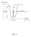
- FIG. 3 is a graph showing a relationship between a difference in frequency between two types of light emitted from alight source section, and the intensity of the light detected in a light receiving section.
- FIG. 4 is a schematic diagram for describing the light source section, an atom cell, and an aperture member provided to the atomic oscillator shown in FIG. 1 .
- FIG. 5 is a diagram showing an example of a relationship between the energy state of a cesium atom, and a resonance light pair (first resonance light, second resonance light) and adjustment light (third resonance light).
- FIGS. 6A and 6B are diagrams each showing a distribution of the magnetic quantum number of a sodium atom, wherein FIG. 6A is a diagram showing the distribution in the case of being irradiated with the resonance light as ⁇ + circularly polarized light, and FIG. 6B is a diagram showing the distribution in the case of being irradiated with the resonance light as ⁇ ⁇ circularly polarized light.
- FIG. 7 is a schematic diagram for describing the light source section, an atom cell, and an aperture member provided to an atomic oscillator according to a second embodiment of the invention.
- FIG. 8 is a schematic diagram for describing the light source section, an atom cell, and an aperture member provided to an atomic oscillator according to a third embodiment of the invention.
- FIG. 9 is a diagram showing a schematic configuration in the case of using the atomic oscillator according to the invention to a positioning system using GPS satellites.
- FIG. 10 is a diagram showing an example of a moving object according to the invention.
- the atomic oscillator (atomic oscillator equipped with the quantum interference device) according to the invention will be described. It should be noted that although an example of applying the quantum interference device according to the invention to the atomic oscillator will hereinafter be described, the quantum interference device according to the invention is not limited to the above, but can be applied to a device such as a magnetic sensor or a quantum memory.
- FIG. 1 is a schematic diagram showing the atomic oscillator (quantum interference device) according to the first embodiment of the invention.
- FIG. 2 is a diagram for schematically describing the energy state of an alkali metal atom.
- FIG. 3 is a graph showing a relationship between a difference in frequency between two types of light emitted from a light source section, and the intensity of the light detected in a light receiving section.
- the atomic oscillator 1 shown in FIG. 1 is an atomic oscillator using coherent population trapping. As shown in FIG. 1 , the atomic oscillator 1 is provided with an atom cell 2 (a gas cell), a light source section 3 , a light receiving section 4 , a heater 5 , a temperature sensor 6 , a magnetic field generation section 7 , and a control section 8 .
- the light source section 3 emits light LL toward the atom cell 2
- the light receiving section 4 detects the light LL having been transmitted through the atom cell 2 .
- the alkali metal has energy levels of a three level system formed of two ground levels (a first ground level and a second ground level) and an excited level.
- the first ground level is an energy state lower than the second ground level.
- the light LL emitted from the light source section 3 includes first resonance light and second resonance light as two types of resonance light different in frequency.
- the light absorptance (the light transmittance) of the first and second resonance light in the alkali metal varies in accordance with a difference ( ⁇ 1 ⁇ 2 ) between the frequency ⁇ 1 of the first resonance light and the frequency ⁇ 2 of the second resonance light.
- the detection intensity of the light receiving section 4 rapidly rises as shown in FIG. 3 when the difference ( ⁇ 1 ⁇ 2 ) between the frequency ⁇ 1 of the first resonance light and the frequency ⁇ 2 of the second resonance light coincides with the frequency ⁇ 0 corresponding to the energy difference ⁇ E between the first ground level and the second ground level.
- a rapid signal as described above is detected as an EIT signal.
- the EIT signal has a characteristic value determined by the type of the alkali metal. Therefore, by using such an EIT signal as a reference, an oscillator high in accuracy can be configured.
- the alkali metal such as rubidium, cesium, or sodium in the form of a gas.
- a noble gas such as argon or neon, or an inert gas such as nitrogen can also be encapsulated together with the alkali metal gas if needed.
- the atom cell 2 has a body part having a through hole, and a pair of window parts closing the openings of the through hole of the body part, and thus, there is formed an internal space in which the gaseous alkali metal is encapsulated.
- the light source section 3 has a function of emitting the light LL including the first resonance light and the second resonance light described above constituting the resonance light pair for resonating the alkali metal atoms in the atom cell 2 .
- the light LL emitted by the light source section 3 includes third resonance light in addition to the first resonance light and the second resonance light.
- the first resonance light is the light (probe light) for exciting the alkali metal atoms located inside the atom cell 2 from the first ground level described above to the excited level.
- the second resonance light is the light (coupling light) for exciting the alkali metal atoms located inside the atom cell 2 from the second ground level described above to the excited level.
- the first resonance light and the second resonance light are circularly polarized in the same direction as each other.
- the third resonance light is the “adjustment light” (repump light) for adjusting the magnetic quantum number of the alkali metal located in the atom cell 2 .
- the third resonance light is circularly polarized in the opposite direction to those of the first resonance light and the second resonance light.
- the “circularly polarized light” denotes the light, in which the vibration direction rotates at the frequency of the light wave in a plane perpendicular to the proceeding direction of the light in focusing attention on the vibration of either one of the electric field component and the magnetic field component of the light wave, and the amplitude of the vibration is constant irrespective of the direction, and in other words, the light in which the vibration of the electric field (or the magnetic field) draws a circle with the propagation.
- the light receiving section 4 has a function of detecting the intensity of the light LL (in particular the resonance light pair formed of the first resonance light and the second resonance light) having been transmitted through the atom cell 2 .
- the light receiving section 4 is not particularly limited as long as the intensity of such light LL as described above can be detected, and for example, a photo detector (a light receiving element) such as a photodiode for outputting a signal corresponding to the intensity of the light received can be used as the light receiving section 4 . It should be noted that a configuration of the light receiving section 4 will be described later in detail.
- the heater 5 (a heating section) has a function of heating the atom cell 2 (more specifically, the alkali metal in the atom cell 2 ) described above.
- the alkali metal located in the atom cell 2 can be kept in the form of a gas with an appropriate density.
- the heater 5 is configured including, for example, a heating resistive element for generating heat in accordance with power distribution.
- the heating resistive element can be disposed so as to have contact with the atom cell 2 , or can also be disposed so as not to have contact with the atom cell 2 .
- the heating resistive element in the case of disposing the heating resistive element so as to have contact with the atom cell 2 , the heating resistive element is disposed on each of a pair of windows of the atom cell 2 .
- the heating resistive element is disposed on each of a pair of windows of the atom cell 2 .
- Such a heating resistive element is formed of a material having permeability with respect to the light LL, specifically a transparent electrode material such as an oxide such as ITO (indium tin oxide), IZO (indium zinc oxide), In 3 O 3 , SnO 2 , Sb-doped SnO 2 , or Al-doped ZnO.
- a heating resistive element can be formed using, for example, a chemical vapor deposition (CVD) such as a plasma CVD or a thermal CVD, a dry plating method such as a vacuum deposition, or a sol-gel method.
- the heating resistive element in the case of disposing the heating resistive element so as not to have contact with the atom cell 2 , it is sufficient to conduct the heat from the heating resistive element to the atom cell 2 via a member made of metal, ceramics, or the like superior in heat conductivity.
- the heater 5 is not limited to the configuration described above as long as the atom cell 2 can be heated, and a variety of types of heaters can be used as the heater 5 . Further, it is also possible to heat the atom cell 2 using a Peltier element instead of, or together with the heater 5 .
- the temperature sensor 6 has a function of detecting the temperature of the heater 5 or the atom cell 2 .
- the temperature sensor 6 is disposed, for example, so as to have contact with the heater 5 or the atom cell 2 .
- the temperature sensor 6 is not particularly limited, and a variety of known temperature sensors such as a thermistor or a thermocouple can be used as the temperature sensor 6 .
- the magnetic field generation section 7 has a function of applying a magnetic field to the alkali metal located in the atom cell 2 .
- the magnetic field generation section 7 has a function of applying a magnetic field to the alkali metal located in the atom cell 2 .
- the magnetic field from the magnetic field generation section 7 is along (roughly parallel to) the proceeding direction of the light LL inside the atom cell 2 .
- the direction of the magnetic field from the magnetic field generation section 7 is preferably in a range of not smaller than 0° and not larger than 30°, more preferably in a range of not smaller than 0° and not larger than 20°, and further more preferably in a range of not smaller than 0° and not larger than 10° with respect to the proceeding direction of the light LL.
- the magnetic field generation section 7 is formed of a coil disposed winding around the outer circumference of the atom cell 2 so as to constitute a solenoidal configuration. It should be noted that the magnetic field generation section 7 can also be constituted by a pair of coils disposed facing to each other across the atom cell 2 so as to constitute a Helmholtz configuration.
- the magnetic field generated by the magnetic field generation section 7 is a constant magnetic field (direct-current magnetic field), but can also be superimposed with an alternating-current magnetic field.
- the control section 8 has a function of controlling each of the light source section 3 , the heater 5 , and the magnetic field generation section 7 .
- the control section 8 has a light source control section 82 for controlling the light source section 3 , a temperature control section 81 for controlling the temperature of the alkali metal in the atom cell 2 , and a magnetic field control section 83 for controlling the magnetic field from the magnetic field generation section 7 .
- the light source control section 82 has a function of controlling the frequencies of the first resonance light and the second resonance light emitted from the light source section 3 based on the detection result of the light receiving section 4 described above. More specifically, the light source control section 82 controls the frequencies of the first resonance light and the second resonance light emitted from the light source section 3 so that the frequency difference ( ⁇ 1 ⁇ 2 ) described above becomes equal to the frequency ⁇ 0 inherent in the alkali metal described above. It should be noted that a configuration of the light source control section 82 will be described later in detail.
- the temperature control section 81 controls the power distribution to the heater 5 based on the detection result of the temperature sensor 6 .
- the atom cell 2 can be kept within the desired temperature range.
- the atom cell 2 is controlled in temperature by the heater 5 to, for example, around 70° C.
- the magnetic field control section 83 controls the power distribution to the magnetic field generation section 7 so that the magnetic field generated by the magnetic field generation section 7 becomes constant.
- Such a control section 8 is disposed in, for example, an IC chip mounted on a board.
- FIG. 4 is a schematic diagram for describing the light source section, the atom cell, and an aperture member provided to the atomic oscillator shown in FIG. 1 .
- the light source section 3 is provided with a first light source section 31 for emitting the resonance light pair LL 1 formed of the first resonance light and the second resonance light as first light, and a second light source section 32 for emitting the adjustment light LL 2 formed of the third resonance light as second light.
- the first light source section 31 has a first light source 311 (a first light emitting element), a lens 312 , a 1 ⁇ 4 wave plate 313 , and an aperture member 34 . It should be noted that the first light source section 31 can also be provided with a 1 ⁇ 2 wave plate disposed between the first light source 311 and the 1 ⁇ 4 wave plate 313 . In this case, it is sufficient to dispose the first light source 311 with a posture rotated 90° around the optical axis.
- the first light source 311 is disposed on the substrate 33 such as a silicon substrate.
- the first light source 311 has a function of emitting first light LL 1 a formed of resonance light pair as linearly polarized light.
- the first light LL 1 a is emitted from the first light source 311 so as to spread with a predetermined radiation angle.
- the radiation angle is not particularly limited, but is preferably in a range of not smaller than 10° and not larger than 40°, and is more preferably in a range of not smaller than 15° and not larger than 30°.
- the first light source 311 is not particularly limited as long as the light including the first light LL 1 a can be emitted, but is a semiconductor laser such as an edge emitting laser or a vertical cavity surface emitting laser (VCSEL).
- VCSEL vertical cavity surface emitting laser
- the “linearly polarized light” is the light having the vibration plane of the magnetic wave (light) in a plane, in other words, the light in which the vibration direction of the electric field (or the magnetic field) is constant.
- the lens 312 is disposed between the first light source 311 and the atom cell 2 .
- the lens 312 is disposed between the first light source 311 and the atom cell 2 .
- the 1 ⁇ 4 wave plate 313 is a birefringent element causing a phase difference of ⁇ /2 (90°) between the polarization components perpendicular to each other of the light having entered the 1 ⁇ 4 wave plate 313 .
- the 1 ⁇ 4 wave plate 313 has a function of converting the first light LL 1 a emitted from the first light source 311 from the linearly polarized light into the resonance light pair LL 1 as the circularly polarized light (including elliptically polarized light).
- the aperture member 34 is disposed on a surface on the first light source 311 side of the 1 ⁇ 4 wave plate 313 .
- the aperture member 34 has an opening 341 for transmitting the light in a partial region out of the light having entered the aperture member 34 , and has a function of adjusting the width (diameter) and the shape of the light.
- a part of the first light LL 1 a from the first light source 311 is transmitted through the opening 341 , and thus, the width and the shape of the first light LL 1 a are adjusted.
- a part of the aperture member 34 excluding the opening 341 is provided with a light blocking property.
- a constituent material of such an aperture member 34 is not particularly limited as long as the part of the aperture member 34 excluding the opening 341 can be provided with the light blocking property, and a resin material or a metal material, for example, can be used as the constituent material, and further, a material with which the part of the aperture member 34 excluding the opening 341 can prevent reflection of the light is preferable as the constituent material.
- the method of forming the aperture member 34 is not particularly limited. In the case of the present embodiment, for example, the aperture member 34 can be formed on the 1 ⁇ 4 wave plate 313 using a known film forming method.
- the first light source section 31 emits the resonance light pair LL 1 using the light from the first light source 311 .
- the second light source section 32 has a second light source 321 , the lens 312 , the 1 ⁇ 4 wave plate 313 , and the aperture member 34 .
- the lens 312 , the 1 ⁇ 4 wave plate 313 , and the aperture member 34 are disposed commonly to the first light source section 31 described above. In other words, it can be said that the lens 312 , the 1 ⁇ 4 wave plate 313 , and the aperture member 34 are provided to the first light source section 31 , and it can also be said that the lens 312 , the 1 ⁇ 4 wave plate 313 , and the aperture member 34 are provided to the second light source section 32 .
- the second light source section 32 can also be provided with a 1 ⁇ 2 wave plate disposed between the second light source 321 and the 1 ⁇ 4 wave plate 313 . In this case, it is sufficient to dispose the second light source 321 with a posture rotated 90° around the optical axis.
- the second light source 321 is disposed on the same substrate 33 as that of the first light source 311 .
- the second light source 321 has a function of emitting second light LL 2 a formed of resonance light linearly polarized in a direction perpendicular to the direction of the linearly polarized light of the first light source 311 .
- the second light LL 2 a is emitted from the second light source 321 so as to spread with a predetermined radiation angle.
- the radiation angle is not particularly limited, but is preferably equivalent to or slightly larger than the radiation angle of the first light LL 1 a in the first light source 311 , and specifically, the radiation angle is preferably in a range of not smaller than 10° and not larger than 50°, and more preferably in a range of not smaller than 15° and not larger than 40°.
- the radiation angle is preferably in a range of not smaller than 10° and not larger than 50°, and more preferably in a range of not smaller than 15° and not larger than 40°.
- the second light source 321 is not particularly limited as long as the light including the second light LL 2 a can be emitted, but is a semiconductor laser such as an edge emitting laser or a vertical cavity surface emitting laser (VCSEL), or a light emitting element such as a light emitting diode (LED), or an organic electroluminescence (organic EL).
- a semiconductor laser such as an edge emitting laser or a vertical cavity surface emitting laser (VCSEL), or a light emitting element such as a light emitting diode (LED), or an organic electroluminescence (organic EL).
- the output (the intensity of the second light LL 2 a ) of the second light source 321 is preferably lower than the output (the intensity of the first light LL 1 a ) of the first light source 311 .
- the output (the intensity of the second light LL 2 a ) of the second light source 321 is preferably lower than the output (the intensity of the first light LL 1 a ) of the first light source 311 .
- the lens 312 is disposed between the second light source 321 and the atom cell 2 .
- the lens 312 is disposed between the second light source 321 and the atom cell 2 .
- the 1 ⁇ 4 wave plate 313 has a function of converting the second light LL 2 a , which has been emitted from the second light source 321 , from the linearly polarized light into the adjustment light LL 2 as the circularly polarized light (including elliptically polarized light).
- the adjustment light LL 2 it is possible to generate the adjustment light LL 2 to be the third resonance light described above.
- the polarization direction of the second light LL 2 a polarized linearly is a direction different from (direction perpendicular to) the polarization direction of the first light LL 1 a polarized linearly.
- the adjustment light LL 2 generated by the 1 ⁇ 4 wave plate 313 is left-handed circularly polarized light
- the adjustment light LL 2 is right-handed circularly polarized light
- the rotational direction of the circularly polarized light as the adjustment light LL 2 becomes the opposite direction to the rotational direction of the circularly polarized light as the resonance light pair LL 1 in the atom cell 2 when viewed from the same direction along the direction in which the window part 22 and the window part 23 of the atom cell 2 are arranged.
- the opening 341 In the second light source section 32 , a part of the second light LL 2 a from the second light source 321 is transmitted through the opening 341 , and thus, the width and the shape of the second light LL 2 a are adjusted.
- the opening 341 when viewed from the direction along an axis line a, it is preferable for the opening 341 to be included in the area where the first light LL 1 a and the second light LL 2 a are superimposed on each other on a plane along the aperture member 34 .
- the second light source section 32 emits the adjustment light LL 2 using the light from the second light source 321 .
- the first light source 311 is controlled by the light source control section 82 so as to emit the first resonance light and the second resonance light described above.
- the light source control section 82 has a frequency control section 821 , voltage controlled crystal oscillators 822 (VCXO), and a phase synchronization circuit (a phase locked loop (PLL)) 823 .
- VCXO voltage controlled crystal oscillators
- PLL phase locked loop
- the frequency control section 821 detects the EIT state in the atom cell 2 based on the received light intensity of the light receiving section 4 to output a control voltage corresponding to the detection result. Thus, the frequency control section 821 controls the voltage controlled crystal oscillator 822 so that the EIT signal is detected by the light receiving section 4 .
- the voltage controlled crystal oscillator 822 is controlled by the frequency control section 821 to oscillate at a predetermined oscillation frequency, and oscillates at a frequency of, for example, about several megahertz through several tens of megahertz. Further, the output signal of the voltage controlled crystal oscillator 822 is input to the phase synchronization circuit 823 , and at the same time, output as the output signal of the atomic oscillator 1 .
- the phase synchronization circuit 823 multiplies the frequency of the output signal from the voltage controlled crystal oscillator 822 .
- the phase synchronization circuit 823 oscillates at a frequency a half as high as the frequency corresponding to the energy difference ⁇ E between the two ground levels different from each other of the alkali metal atom described above.
- the signal (the high-frequency signal) multiplied in such a manner as described above is input to the first light source 311 of the first light source section 31 as the drive signal after the direct-current bias current is overlapped on the signal thus multiplied.
- the light emitting element such as a semiconductor laser included in the first light source 311 to make the light emitting element emit the first resonance light and the second resonance light as the two types of light having the frequency difference ( ⁇ 1 ⁇ 2 ) equal to ⁇ 0 .
- the current value of the direct-current bias current is controlled by a bias control section not shown to a predetermined value.
- a bias control section not shown to a predetermined value.
- first light source 311 and the second light source 321 are each adjusted in temperature to a predetermined temperature using a temperature control element (e.g., a heating resistive element or a Peltier element) not shown. Further, by controlling the temperature of the first light source 311 and the second light source 321 , it is also possible to control the central wavelength of the light from the first light source 311 and the second light source 321 .
- a temperature control element e.g., a heating resistive element or a Peltier element
- the atom cell 2 is irradiated with the resonance light pair LL 1 and the adjustment light LL 2 from the first light source section 31 and the second light source section 32 configured in such a manner as explained hereinabove.
- the atom cell 2 has the body section 21 , and the pair of window parts 22 , 23 disposed across the body part 21 from each other.
- the body part 21 is disposed between the pair of window parts 22 , 23 , and the body part 21 and the pair of window parts 22 , 23 compartment (form) an internal space S in which the gaseous alkali metal is encapsulated.
- the body part 21 has a plate-like shape, and the body part 21 is provided with the through hole 211 penetrating the body part 21 in the thickness direction.
- the constituent material of the body part 21 is not particularly limited, and there can be cited a glass material, a quartz crystal, a metal material, a resin material, a silicon material, and so on as the constituent material of the body part 21 .
- a glass material a quartz crystal, a metal material, a resin material, a silicon material, and so on
- either of the glass material, the quartz crystal, and the silicon material is preferably used, and the silicon material is further preferably used.
- a microfabrication technology such as etching.
- the microfabrication by etching can be performed on silicon.
- the body part 21 can easily and accurately be formed.
- the window parts 22 , 23 are generally formed of glass, silicon is superior in thermal conductivity compared to glass. Therefore, it is possible to make the heat radiation property of the body part 21 excellent. Further, in the case in which the window parts 22 , 23 are formed of glass, the body part 21 and the window parts 22 , 23 can airtightly be bonded to each other with ease using anodic bonding, and thus the reliability of the atom cell 2 can be made excellent.
- the bonding method between the body part 21 and the window parts 22 , 23 is determined in accordance with the constituent materials of these parts, and is not particularly limited as long as the body part 21 and the window parts 22 , 23 can airtightly be bonded to each other.
- the bonding method there can be used, for example, a bonding method using an adhesive, a direct bonding method, an anodic bonding method, and a surface activated bonding method, and the direct bonding method or the anodic bonding method is preferably used.
- the body part 21 and the window parts 22 , 23 can airtightly be bonded to each other with ease, and the reliability of the atom cell 2 can be made excellent.
- the window parts 22 , 23 bonded to such a body part 21 each have a plate-like shape, and have permeability with respect to the light LL from the light source part 3 described above. Further, one of the window parts, namely the window part 22 , is an incident side window part through which the resonance light pair LL 1 and the adjustment light LL 2 enter the internal space S of the atom cell 2 , and the other of the window parts, namely the window part 23 , is an exit side window part through which the resonance light pair LL 1 and the adjustment light LL 2 are emitted from the internal space S of the atom cell 2 .
- the constituent material of the window parts 22 , 23 is not particularly limited as long as the constituent material has such permeability with respect to the light LL as described above, and as the constituent material of the window parts 22 , 23 , there can be cited, for example, a glass material and a quartz crystal, and the glass material is preferably used. Thus, there can be realized the window parts 22 , 23 having the permeability with respect to the excitation light. Further, in the case in which the body part 21 is formed of silicon, by forming the window parts 22 , 23 using glass, the body part 21 and the window parts 22 , 23 can airtightly be bonded to each other with ease using anodic bonding, and thus the reliability of the atom cell 2 can be made excellent.
- the window parts 22 , 23 can be formed of silicon. Even in this case, the body part 21 and the window parts 22 , 23 can directly or anodically be bonded to each other.
- the gaseous alkali metal housed in the internal space S is excited by the light LL.
- at least part of the internal space S constitutes a “light passing space” through which the light LL passes.
- the coil 71 as a solenoidal coil provided to the magnetic field generation section 7 .
- the passing area of the resonance light pair LL 1 it is preferable for the passing area of the resonance light pair LL 1 to coincide with or to be included in the passing area of the adjustment light LL 2 .
- the respective light axes of the resonance light pair LL 1 and the adjustment light LL 2 are parallel to the axis line a along the direction in which the window part 22 and the window part 23 of the atom cell 2 are arranged.
- the respective light axes of the resonance light pair LL 1 and the adjustment light LL 2 are allowed to be tilted with respect to the axis line a.
- the light receiving section 4 described above is disposed on the axis line a or the extension of the axis line, and the resonance light pair LL 1 having passed through the atom cell 2 is received by the light receiving section 4 .
- the adjustment light LL 2 having passed through the atom cell 2 it is preferable for the adjustment light LL 2 having passed through the atom cell 2 not to be received by the light receiving part 4 .
- a filter for preventing the passage of the adjustment light LL 2 while allowing the passage of the resonance light pair LL 1 between the atom cell 2 and the light receiving section 4 there can be cited, for example, a device having a 1 ⁇ 4 wave plate and a polarizer arranged in this order from the atom cell 2 side toward the light receiving section 4 side.
- FIG. 5 is a diagram showing an example of a relationship between the energy state of a cesium atom, and the resonance light pair (the first resonance light, the second resonance light) and the adjustment light (the third resonance light).
- FIGS. 6A and 6B are diagrams each showing a distribution of the magnetic quantum number of a sodium atom, wherein FIG. 6A is a diagram showing the distribution in the case of being irradiated with the resonance light as ⁇ + circularly polarized light, and FIG. 6B is a diagram showing the distribution in the case of being irradiated with the resonance light as ⁇ ⁇ circularly polarized light.
- the function of the resonance light pair and the adjustment light in such a case will hereinafter be described based on FIGS. 5, 6A, and 6B .
- the D1 line which is ⁇ + -polarized (left-handed circularly polarized)
- the D2 line which is ⁇ ⁇ -polarized (right-handed circularly polarized)
- first resonance light and the second resonance light are each the ⁇ ⁇ -polarized light
- the third resonance light is the ⁇ + -polarized light
- the first resonance light and the second resonance light are each the D2 line
- the third resonance light is the D1 line.
- the wavelength of the D1 line in vacuum is 894.593 nm
- the wavelength of the D2 line in vacuum is 852.347 nm
- the hyperfine splitting frequency ( ⁇ E) of 6S 1/2 is 9.1926 GHz.
- the alkali metal atoms other than the cesium atoms also have two ground levels and an excited level constituting the ⁇ -type three levels in a similar manner.
- the wavelength of the D1 line in vacuum is 589.756 nm
- the wavelength of the D2 line in vacuum is 589.158 nm
- the hyperfine splitting frequency ( ⁇ E) of 3S 1/2 is 1.7716 GHz.
- the wavelength of the D1 line in vacuum is 794.979 nm
- the wavelength of the D2 line in vacuum is 780.241 nm
- the hyperfine splitting frequency ( ⁇ E) of 5S 1/2 is 3.0357 GHz.
- the wavelength of the D1 line in vacuum is 794.979 nm
- the wavelength of the D2 line in vacuum is 780.241 nm
- the hyperfine splitting frequency ( ⁇ E) of 5S 1/2 is 6.8346 GHz.
- the sodium atom which is a kind of the alkali metal atom, has the two ground levels and the excited level constituting the ⁇ -type three levels
- each of the ground levels and the excited level has 2F+1 magnetic quantum numbers (magnetic sublevels), and the distribution of the magnetic quantum number changes under the selection rule as described above.
- the bias of the magnetic quantum number of the alkali metal can be reduced.
- the bias in the distribution of the magnetic quantum number due to the resonance light pair LL 1 can be canceled out or reduced by the adjustment light LL 2 to thereby reduce the bias in the distribution of the magnetic quantum number of the alkali metal.
- the number of the alkali metal atoms having the desired magnetic quantum number making a contribution to the EIT is increased, and as a result, the advantage of increasing the strength of the EIT signal is markedly developed by using the resonance light pair LL 1 circularly polarized, and thus, it is possible to effectively increase the strength of the EIT signal.
- the aperture member 34 having the opening 341 is disposed between the internal space S, and the first light source 311 (the first light emitting element) and the second light source 321 (the second light emitting element), the passing areas of the resonance light pair LL 1 (first light) and the adjustment light LL 2 (second light) entering the internal space S of the atom cell 2 can be made to coincide with or approximate to each other. Therefore, the bias in the distribution of the magnetic quantum number of the alkali metal can efficiently be reduced.
- the atom cell 2 it is possible to achieve homogenization of the light intensity density (power density) in the respective width directions of the resonance light pair LL 1 and the adjustment light LL 2 , and at the same time, to reduce the area through which only either one of the resonance light pair LL 1 and the adjustment light LL 2 passes. Therefore, the balance between the resonance light pair LL 1 and the adjustment light LL 2 can be made excellent, and thus, the strength of the EIT signal can be increased while decreasing the linewidth of the EIT signal.
- each of the resonance light pair LL 1 and the adjustment light LL 2 entering the internal space S of the atom cell 2 can be made into parallel light. Therefore, it is possible to reduce the chance for the power density of the resonance light pair LL 1 and the adjustment light LL 2 to vary in the proceeding direction (a propagating direction) in the internal space S of the atom cell 2 to thereby efficiently reduce the bias in the distribution of the magnetic quantum number of the alkali metal. As a result, it is possible to increase the strength of the EIT signal while narrowing the linewidth of the EIT signal.
- the aperture member 34 is eliminated, the area through which only the resonance light pair LL 1 or only the adjustment light LL 2 passes is apt to increase in the internal space S of the atom cell 2 . Therefore, in the case in which the first light source 311 and the second light source 321 are disposed on the same substrate 33 , the advantage obtained by disposing the aperture member 34 becomes conspicuous.
- the first light source section 31 and the second light source section 32 are commonly provided with the 1 ⁇ 4 wave plate 313 disposed between the first light source 311 and the second light source 321 , and the internal space S.
- the resonance light pair LL 1 from the first light source section 31
- the adjustment light LL 2 from the second light source section 32 while reducing the number of components constituting the first light source section 31 and the second light source section 32 .
- the aperture member 34 is disposed between the first light source 311 and the second light source 321 , and the 1 ⁇ 4 wave plate 313 , it is possible to reduce the chance for the light failing to enter the opening 341 of the aperture member 34 to be reflected by the 1 ⁇ 4 wave plate 313 to exert a harmful influence.
- the aperture member 34 is disposed on the 1 ⁇ 4 wave plate 313 , the aperture member 34 and the 1 ⁇ 4 wave plate 313 can be disposed in a lump, and thus, manufacturing of the atomic oscillator 1 becomes easy.
- one of the resonance light pair LL 1 and the adjustment light LL 2 is the D1 line, and the other is the D2 line, it is possible to efficiently cause the EIT phenomenon, and as a result, it is possible to efficiently increase the strength of the EIT signal.
- the intensity (the photon flux density) of the adjustment light LL 2 is lower than that of the resonance light pair LL 1 in the atom cell 2 .
- the bias in the magnetic quantum number of the alkali metal in the atom cell 2 can efficiently be reduced.
- the intensity of the adjustment light LL 2 is too high, the distribution of the magnetic quantum number of the alkali metal in the atom cell 2 is dramatically biased toward the opposite side to the bias in the distribution of the magnetic quantum number due to the resonance light pair LL 1 in some cases.
- the intensity of the adjustment light LL 2 is too low, the bias in the distribution of the magnetic quantum number due to the resonance light pair LL 1 cannot sufficiently be canceled out or reduced by the adjustment light LL 2 in some cases.
- D2/D1 is preferably not lower than 0.1 and not higher than 0.9, more preferably not lower than 0.2 and not higher than 0.7, and further more preferably not lower than 0.3 and not higher than 0.5.
- the resonance light pair LL 1 having a desired frequency can easily be generated. Further, since the surface emitting laser emits the light spreading with a predetermined radiation angle, it is possible to easily superimpose the light from the first light source 311 and the light from the second light source 321 on each other to make the result enter the aperture member 34 .
- the adjustment light LL 2 having a desired frequency can easily be generated.
- the surface emitting laser emits the light spreading with a predetermined radiation angle, it is possible to easily superimpose the light from the first light source 311 and the light from the second light source 321 on each other to make the result enter the aperture member 34 .
- the linewidth of the adjustment light LL 2 can be made larger than that of the resonance light pair LL 1 . Therefore, it is possible to resonate the adjustment light LL 2 with respect to the alkali metal atom broad in velocity distribution. Therefore, if the central wavelength of the adjustment light LL 2 has some minor deviations, it is possible to resonate the adjustment light LL 2 with respect to the alkali metal atom at a desired velocity. As a result, the frequency control of the adjustment light LL 2 becomes unnecessary, and the device configuration can be simplified. Further, since the light emitting diode emits the light spreading with a predetermined radiation angle, it is possible to easily superimpose the light from the first light source 311 and the light from the second light source 321 on each other to make the result enter the aperture member 34 .
- FIG. 7 is a schematic diagram for describing the light source section, an atom cell, and an aperture member provided to an atomic oscillator according to the second embodiment of the invention.
- the present embodiment is substantially the same as the first embodiment described above except the point that the lens disposed between the first light emitting element and the second light emitting element is omitted, and the atom cell is omitted.
- the atomic oscillator 1 A shown in FIG. 7 is substantially the same as the atomic oscillator 1 according to the first embodiment except the point that the lens 312 of the first embodiment described above is omitted.
- the atomic oscillator 1 A is provided with a first light source section 31 A constituted by the first light source 311 , the 1 ⁇ 4 wave plate 313 , and the aperture member 34 , and a second light source section 32 A constituted by the second light source 321 , the 1 ⁇ 4 wave plate 313 , and the aperture member 34 .
- the resonance light pair LL 1 and the adjustment light LL 2 also pass through the atom cell 2 while spreading. Therefore, the power densities of the resonance light pair LL 1 and the adjustment light LL 2 vary in the proceeding direction in the atom cell 2 . In order to reduce the influence of such a variation in the power density, it is sufficient to decrease the length in the direction along the axis line a of the atom cell 2 .
- the strength of the EIT signal can effectively be increased.
- FIG. 8 is a schematic diagram for describing the light source section, an atom cell, and an aperture member provided to an atomic oscillator according to the third embodiment of the invention.
- the present embodiment is substantially the same as the first embodiment described above except the point that the arrangement of the aperture member is different.
- the atomic oscillator 1 B shown in FIG. 8 is provided with a first light source section 31 B constituted by the first light source 311 , the lens 312 , the 1 ⁇ 4 wave plate 313 , and an aperture member 34 B, and a second light source section 32 B constituted by the second light source 321 , the lens 312 , the 1 ⁇ 4 wave plate 313 , and the aperture member 34 B.
- the aperture member 34 B is disposed between the 1 ⁇ 4 wave plate 313 and the internal space S.
- the distance between the aperture member 34 B and the internal space S can be shortened. Therefore, the adjustment of the shapes of the passing areas of the resonance light pair LL 1 and the adjustment light LL 2 entering the internal space S of the atom cell 2 becomes easy.
- the aperture member 34 B is disposed on the atom cell 2 .
- the aperture member 34 B and the atom cell 2 can be disposed in a lump, and manufacturing of the atomic oscillator 1 B becomes easy. Further, it is possible to reduce the chance for the position of the opening 341 of the aperture member 34 B with respect to the internal space S of the atom cell 2 to fluctuate.
- the strength of the EIT signal can effectively be increased.
- Such an atomic oscillator as described hereinabove can be incorporated in a variety of electronic apparatuses.
- FIG. 9 is a diagram showing a schematic configuration in the case of using the atomic oscillator according to the invention to a positioning system using GPS satellites.
- the positioning system 100 shown in FIG. 9 is constituted by GPS satellites 200 , a base station device 300 , and a GPS receiving device 400 .
- the GPS satellites 200 each transmit positioning information (a GPS signal).
- the base station device 300 is provided with a receiving device 302 for accurately receiving the positioning information from the GPS satellites 200 via an antenna 301 installed at, for example, an electronic reference point (a GPS continuous observation station), and a transmitting device 304 for transmitting the positioning information, which has been received by the receiving device 302 , via an antenna 303 .
- a receiving device 302 for accurately receiving the positioning information from the GPS satellites 200 via an antenna 301 installed at, for example, an electronic reference point (a GPS continuous observation station), and a transmitting device 304 for transmitting the positioning information, which has been received by the receiving device 302 , via an antenna 303 .
- the receiving device 302 is an electronic device equipped with the atomic oscillator 1 according to the invention described above as a reference frequency oscillation source for the receiving device 302 . Such a receiving device 302 has excellent reliability. Further, the positioning information having been received by the receiving device 302 is transmitted by the transmitting device 304 in real time.
- the GPS receiving device 400 is provided with a satellite receiving section 402 for receiving the positioning information from the GPS satellites 200 via an antenna 401 , and a base station receiving section 404 for receiving the positioning information from the base station device 300 via an antenna 403 .
- FIG. 10 is a diagram showing an example of the moving object according to the invention.
- the moving object 1500 has a vehicle body 1501 , and four wheels 1502 , and is configured to rotate the wheels 1502 by a power source (an engine) not shown provided to the vehicle body 1501 .
- a power source an engine
- Such a moving object 1500 incorporates the atomic oscillator 1 .
- the electronic apparatus according to the invention is not limited to those described above, and as the electronic apparatus according to the invention, there can be cited, for example, a smartphone, a tablet terminal, a timepiece, a cellular phone, a digital still camera, an inkjet ejection device (e.g., an inkjet printer), a personal computer (a mobile personal computer and a laptop personal computer), a television set, a video camera, a video cassette recorder, a car navigation system, a pager, a personal digital assistance (including one with a communication function), an electronic dictionary, an electric calculator, a computerized game machine, a word processor, a workstation, a video phone, a security video monitor, a pair of electronic binoculars, a POS terminal, a medical device (e.g., an electronic thermometer, an electronic manometer, an electronic blood sugar meter, an electrocardiogram measurement instrument, an ultrasonograph, and an electronic endoscope), a fish detector, various types of measurement instruments, various types
- the quantum interference device the atomic oscillator, the electronic apparatus, and the moving object according to the invention are hereinabove described based on the embodiments shown in the accompanying drawings, the invention is not limited to the embodiments.
- each of the sections of the invention can be replaced with an arbitrary configuration having substantially the same function, and further, it is also possible to add an arbitrary constituent. Further, the invention can be a combination of any of constituents in each of the embodiments described above.
Landscapes
- Physics & Mathematics (AREA)
- General Physics & Mathematics (AREA)
- Nonlinear Science (AREA)
- Spectroscopy & Molecular Physics (AREA)
- Life Sciences & Earth Sciences (AREA)
- Ecology (AREA)
- Optics & Photonics (AREA)
- Stabilization Of Oscillater, Synchronisation, Frequency Synthesizers (AREA)
Abstract
Description
Claims (20)
Applications Claiming Priority (2)
| Application Number | Priority Date | Filing Date | Title |
|---|---|---|---|
| JP2015160325A JP6544132B2 (en) | 2015-08-17 | 2015-08-17 | Quantum interference device, atomic oscillator, and electronic device |
| JP2015-160325 | 2015-08-17 |
Publications (2)
| Publication Number | Publication Date |
|---|---|
| US20170054446A1 US20170054446A1 (en) | 2017-02-23 |
| US9935642B2 true US9935642B2 (en) | 2018-04-03 |
Family
ID=58157961
Family Applications (1)
| Application Number | Title | Priority Date | Filing Date |
|---|---|---|---|
| US15/236,714 Active US9935642B2 (en) | 2015-08-17 | 2016-08-15 | Quantum interference device, atomic oscillator, electronic apparatus, and moving object |
Country Status (3)
| Country | Link |
|---|---|
| US (1) | US9935642B2 (en) |
| JP (1) | JP6544132B2 (en) |
| CN (1) | CN106470035B (en) |
Families Citing this family (3)
| Publication number | Priority date | Publication date | Assignee | Title |
|---|---|---|---|---|
| JP6841190B2 (en) * | 2017-08-31 | 2021-03-10 | セイコーエプソン株式会社 | Frequency signal generator and frequency signal generator |
| CN112763794B (en) * | 2020-12-09 | 2023-08-15 | 北京无线电计量测试研究所 | Quantum power detection module |
| CN114487621B (en) * | 2022-01-22 | 2025-03-07 | 山西大学 | A continuous frequency electric field measurement device and method based on Rydberg atom AC Stark effect |
Citations (9)
| Publication number | Priority date | Publication date | Assignee | Title |
|---|---|---|---|---|
| US7378913B2 (en) | 2003-11-26 | 2008-05-27 | Kernco, Inc. | Optically excited atomic frequency standard |
| US7379486B2 (en) * | 2005-07-22 | 2008-05-27 | Honeywell International Inc. | Technique for optically pumping alkali-metal atoms using CPT resonances |
| US8237514B2 (en) | 2009-02-06 | 2012-08-07 | Seiko Epson Corporation | Quantum interference device, atomic oscillator, and magnetic sensor |
| JP2014017824A (en) | 2009-02-06 | 2014-01-30 | Seiko Epson Corp | Quantum interference device, atomic oscillator and magnetic sensor |
| US20150042327A1 (en) | 2013-08-06 | 2015-02-12 | Northrop Grumman Systems Corporation | Probe beam frequency stabilization in an atomic sensor system |
| JP2015062020A (en) | 2014-10-27 | 2015-04-02 | セイコーエプソン株式会社 | Magnetic measuring device and biological state measuring device |
| JP2015082763A (en) | 2013-10-23 | 2015-04-27 | セイコーエプソン株式会社 | Optical module and atomic oscillator |
| US20150180489A1 (en) * | 2013-12-20 | 2015-06-25 | Seiko Epson Corporation | Quantum interference device, atomic oscillator, electronic apparatus, and moving object |
| US20160105150A1 (en) * | 2014-10-14 | 2016-04-14 | Seiko Epson Corporation | Quantum interference device, atomic oscillator, electronic device, and moving object |
Family Cites Families (10)
| Publication number | Priority date | Publication date | Assignee | Title |
|---|---|---|---|---|
| JPH10303478A (en) * | 1997-04-30 | 1998-11-13 | Nec Corp | Cavity for rubidium atomic oscillator |
| US7102451B2 (en) * | 2004-02-18 | 2006-09-05 | Princeton University, Office Of Technology, Licensing & Intellectual Property | Method and system for operating an atomic clock with alternating-polarization light |
| KR100559185B1 (en) * | 2004-10-14 | 2006-03-10 | 한국표준과학연구원 | Laser frequency stabilization method and apparatus using electromagnetic inductive permeability |
| JP2010147967A (en) * | 2008-12-22 | 2010-07-01 | Epson Toyocom Corp | Atomic oscillator and method of stabilizing frequency thereof |
| EP2498150A1 (en) * | 2011-03-09 | 2012-09-12 | CSEM Centre Suisse D'electronique Et De Microtechnique SA | Atomic clock |
| JP6346446B2 (en) * | 2013-02-14 | 2018-06-20 | 株式会社リコー | Atomic oscillator, CPT resonance detection method, and magnetic sensor |
| JP6179327B2 (en) * | 2013-09-30 | 2017-08-16 | セイコーエプソン株式会社 | Quantum interference devices, atomic oscillators, electronic equipment, and moving objects |
| JP2015089055A (en) * | 2013-11-01 | 2015-05-07 | セイコーエプソン株式会社 | Optical module and atomic oscillator |
| JP2015118962A (en) * | 2013-12-16 | 2015-06-25 | セイコーエプソン株式会社 | Quantum interference devices, atomic oscillators, electronic equipment, and moving objects |
| JP6287169B2 (en) * | 2013-12-20 | 2018-03-07 | セイコーエプソン株式会社 | Quantum interference devices, atomic oscillators, electronic equipment, and moving objects |
-
2015
- 2015-08-17 JP JP2015160325A patent/JP6544132B2/en active Active
-
2016
- 2016-08-05 CN CN201610638372.6A patent/CN106470035B/en active Active
- 2016-08-15 US US15/236,714 patent/US9935642B2/en active Active
Patent Citations (11)
| Publication number | Priority date | Publication date | Assignee | Title |
|---|---|---|---|---|
| US7378913B2 (en) | 2003-11-26 | 2008-05-27 | Kernco, Inc. | Optically excited atomic frequency standard |
| US7379486B2 (en) * | 2005-07-22 | 2008-05-27 | Honeywell International Inc. | Technique for optically pumping alkali-metal atoms using CPT resonances |
| US8237514B2 (en) | 2009-02-06 | 2012-08-07 | Seiko Epson Corporation | Quantum interference device, atomic oscillator, and magnetic sensor |
| JP2014017824A (en) | 2009-02-06 | 2014-01-30 | Seiko Epson Corp | Quantum interference device, atomic oscillator and magnetic sensor |
| US8643441B2 (en) * | 2009-02-06 | 2014-02-04 | Seiko Epson Corporation | Quantum interference device, atomic oscillator, and magnetic sensor |
| US20150042327A1 (en) | 2013-08-06 | 2015-02-12 | Northrop Grumman Systems Corporation | Probe beam frequency stabilization in an atomic sensor system |
| JP2015042977A (en) | 2013-08-06 | 2015-03-05 | ノースロップ グルマン システムズ コーポレーションNorthrop Grumman Systems Corporation | Atomic sensor system and method for stabilizing probe beam frequency thereof |
| JP2015082763A (en) | 2013-10-23 | 2015-04-27 | セイコーエプソン株式会社 | Optical module and atomic oscillator |
| US20150180489A1 (en) * | 2013-12-20 | 2015-06-25 | Seiko Epson Corporation | Quantum interference device, atomic oscillator, electronic apparatus, and moving object |
| US20160105150A1 (en) * | 2014-10-14 | 2016-04-14 | Seiko Epson Corporation | Quantum interference device, atomic oscillator, electronic device, and moving object |
| JP2015062020A (en) | 2014-10-27 | 2015-04-02 | セイコーエプソン株式会社 | Magnetic measuring device and biological state measuring device |
Also Published As
| Publication number | Publication date |
|---|---|
| CN106470035A (en) | 2017-03-01 |
| US20170054446A1 (en) | 2017-02-23 |
| CN106470035B (en) | 2021-07-09 |
| JP6544132B2 (en) | 2019-07-17 |
| JP2017041662A (en) | 2017-02-23 |
Similar Documents
| Publication | Publication Date | Title |
|---|---|---|
| US10027335B2 (en) | Quantum interference device, atomic oscillator, electronic device, and moving object | |
| US9507322B2 (en) | Atomic cell manufacturing method, atomic cell, quantum interference device, atomic oscillator, electronic device, and moving object | |
| US10396810B2 (en) | Quantum interference device, atomic oscillator, electronic apparatus, and moving object | |
| US10133095B2 (en) | Quantum interference device, atomic oscillator, electronic apparatus, and moving object comprising FM-modulated adjustment light | |
| US9312871B2 (en) | Gas cell, quantum interference device, atomic oscillator, electronic device, and moving object | |
| US9577652B2 (en) | Atomic resonance transition device, atomic oscillator, electronic apparatus, and moving object | |
| JP6484922B2 (en) | Atomic cell, quantum interference device, atomic oscillator and electronic equipment | |
| US9935642B2 (en) | Quantum interference device, atomic oscillator, electronic apparatus, and moving object | |
| JP6520039B2 (en) | Quantum interference device, atomic oscillator and electronic device | |
| US9503110B2 (en) | Gas cell, quantum interference device, atomic oscillator, electronic device, and moving object | |
| JP6442969B2 (en) | Quantum interference devices, atomic oscillators, and electronic equipment | |
| US10326461B2 (en) | Quantum interference device, atomic oscillator, electronic apparatus, and moving object | |
| JP2017152514A (en) | Quantum interference device, atomic oscillator, electronic device, and moving object | |
| JP6264876B2 (en) | Quantum interference devices, atomic oscillators, and electronic equipment | |
| JP6627335B2 (en) | Quantum interference devices, atomic oscillators, and electronics | |
| JP2014099728A (en) | Atomic oscillator, method of adjusting characteristic of atomic oscillator, electronic apparatus, and mobile body | |
| JP6565397B2 (en) | Quantum interference devices, atomic oscillators, and electronic equipment | |
| JP6662061B2 (en) | Quantum interference devices, atomic oscillators, electronic equipment and moving objects | |
| JP2017022653A (en) | Quantum interference device, atomic oscillator, electronic apparatus and movable body |
Legal Events
| Date | Code | Title | Description |
|---|---|---|---|
| AS | Assignment |
Owner name: SEIKO EPSON CORPORATION, JAPAN Free format text: ASSIGNMENT OF ASSIGNORS INTEREST;ASSIGNORS:HAYASHI, NOBUHITO;MAKI, YOSHIYUKI;REEL/FRAME:039433/0620 Effective date: 20160706 |
|
| STCF | Information on status: patent grant |
Free format text: PATENTED CASE |
|
| MAFP | Maintenance fee payment |
Free format text: PAYMENT OF MAINTENANCE FEE, 4TH YEAR, LARGE ENTITY (ORIGINAL EVENT CODE: M1551); ENTITY STATUS OF PATENT OWNER: LARGE ENTITY Year of fee payment: 4 |
|
| AS | Assignment |
Owner name: MICROCHIP TECHNOLOGY INCORPORATED, ARIZONA Free format text: ASSIGNMENT OF ASSIGNORS INTEREST;ASSIGNOR:SEIKO EPSON CORPORATION;REEL/FRAME:061301/0770 Effective date: 20220707 |
|
| MAFP | Maintenance fee payment |
Free format text: PAYMENT OF MAINTENANCE FEE, 8TH YEAR, LARGE ENTITY (ORIGINAL EVENT CODE: M1552); ENTITY STATUS OF PATENT OWNER: LARGE ENTITY Year of fee payment: 8 |