US9934171B2 - Serial communication link with optimal transfer latency - Google Patents
Serial communication link with optimal transfer latency Download PDFInfo
- Publication number
- US9934171B2 US9934171B2 US15/040,271 US201615040271A US9934171B2 US 9934171 B2 US9934171 B2 US 9934171B2 US 201615040271 A US201615040271 A US 201615040271A US 9934171 B2 US9934171 B2 US 9934171B2
- Authority
- US
- United States
- Prior art keywords
- signals
- frame
- gpio
- changed
- bit
- Prior art date
- Legal status (The legal status is an assumption and is not a legal conclusion. Google has not performed a legal analysis and makes no representation as to the accuracy of the status listed.)
- Active, expires
Links
- 238000004891 communication Methods 0.000 title description 7
- 238000012546 transfer Methods 0.000 title description 2
- 230000005540 biological transmission Effects 0.000 claims description 53
- 238000000034 method Methods 0.000 claims description 17
- 230000001413 cellular effect Effects 0.000 claims description 2
- 230000000737 periodic effect Effects 0.000 claims 1
- 230000009467 reduction Effects 0.000 description 9
- 230000002093 peripheral effect Effects 0.000 description 7
- 230000010355 oscillation Effects 0.000 description 6
- 238000010586 diagram Methods 0.000 description 5
- 230000008859 change Effects 0.000 description 4
- 230000006870 function Effects 0.000 description 4
- 230000011664 signaling Effects 0.000 description 4
- 240000007320 Pinus strobus Species 0.000 description 3
- 230000001960 triggered effect Effects 0.000 description 3
- 230000008901 benefit Effects 0.000 description 2
- 238000007599 discharging Methods 0.000 description 2
- 238000013461 design Methods 0.000 description 1
- 238000001514 detection method Methods 0.000 description 1
- 230000036541 health Effects 0.000 description 1
- 230000006872 improvement Effects 0.000 description 1
- 230000003993 interaction Effects 0.000 description 1
- 230000004048 modification Effects 0.000 description 1
- 238000012986 modification Methods 0.000 description 1
- 230000008569 process Effects 0.000 description 1
- 230000004044 response Effects 0.000 description 1
- 238000006467 substitution reaction Methods 0.000 description 1
Images


Classifications
-
- G—PHYSICS
- G06—COMPUTING; CALCULATING OR COUNTING
- G06F—ELECTRIC DIGITAL DATA PROCESSING
- G06F13/00—Interconnection of, or transfer of information or other signals between, memories, input/output devices or central processing units
- G06F13/14—Handling requests for interconnection or transfer
- G06F13/16—Handling requests for interconnection or transfer for access to memory bus
- G06F13/1605—Handling requests for interconnection or transfer for access to memory bus based on arbitration
- G06F13/161—Handling requests for interconnection or transfer for access to memory bus based on arbitration with latency improvement
-
- G—PHYSICS
- G06—COMPUTING; CALCULATING OR COUNTING
- G06F—ELECTRIC DIGITAL DATA PROCESSING
- G06F13/00—Interconnection of, or transfer of information or other signals between, memories, input/output devices or central processing units
- G06F13/10—Program control for peripheral devices
- G06F13/12—Program control for peripheral devices using hardware independent of the central processor, e.g. channel or peripheral processor
- G06F13/124—Program control for peripheral devices using hardware independent of the central processor, e.g. channel or peripheral processor where hardware is a sequential transfer control unit, e.g. microprocessor, peripheral processor or state-machine
- G06F13/126—Program control for peripheral devices using hardware independent of the central processor, e.g. channel or peripheral processor where hardware is a sequential transfer control unit, e.g. microprocessor, peripheral processor or state-machine and has means for transferring I/O instructions and statuses between control unit and main processor
-
- G—PHYSICS
- G06—COMPUTING; CALCULATING OR COUNTING
- G06F—ELECTRIC DIGITAL DATA PROCESSING
- G06F13/00—Interconnection of, or transfer of information or other signals between, memories, input/output devices or central processing units
- G06F13/38—Information transfer, e.g. on bus
- G06F13/40—Bus structure
- G06F13/4004—Coupling between buses
- G06F13/4009—Coupling between buses with data restructuring
- G06F13/4018—Coupling between buses with data restructuring with data-width conversion
-
- G—PHYSICS
- G06—COMPUTING; CALCULATING OR COUNTING
- G06F—ELECTRIC DIGITAL DATA PROCESSING
- G06F13/00—Interconnection of, or transfer of information or other signals between, memories, input/output devices or central processing units
- G06F13/38—Information transfer, e.g. on bus
- G06F13/42—Bus transfer protocol, e.g. handshake; Synchronisation
- G06F13/4282—Bus transfer protocol, e.g. handshake; Synchronisation on a serial bus, e.g. I2C bus, SPI bus
- G06F13/4291—Bus transfer protocol, e.g. handshake; Synchronisation on a serial bus, e.g. I2C bus, SPI bus using a clocked protocol
-
- G—PHYSICS
- G06—COMPUTING; CALCULATING OR COUNTING
- G06F—ELECTRIC DIGITAL DATA PROCESSING
- G06F15/00—Digital computers in general; Data processing equipment in general
- G06F15/76—Architectures of general purpose stored program computers
- G06F15/78—Architectures of general purpose stored program computers comprising a single central processing unit
- G06F15/7807—System on chip, i.e. computer system on a single chip; System in package, i.e. computer system on one or more chips in a single package
- G06F15/7817—Specially adapted for signal processing, e.g. Harvard architectures
Definitions
- This application relates to serial communication, and more particularly to a serial communication link with optimal transfer latency.
- Serial communication interfaces are a common element for an integrated circuit processor such as a system on a chip (SoC).
- SoC system on a chip
- An SoC must serve an ever expanding set of functions such as web browsing, email, video gaming, and so on.
- To interface with its various peripherals during the execution of these functions requires a certain number of pins or terminals. It would be convenient to assign each input/output signal to its own unique pin but increasing the number of pins for an integrated circuit increases its costs. Moreover, even if cost were no issue, an integrated circuit can only fit so many pins onto its surfaces.
- conventional SoCs typically include have one or more serial communication interfaces such as a universal asynchronous receiver transmitter (UART) interface, an inter-integrated circuit (I2C or I3C) interface, or a serial peripheral interface (SPI).
- UART universal asynchronous receiver transmitter
- I2C or I3C inter-integrated circuit
- SPI serial peripheral interface
- serial interfaces are thus advantageous, the serialization of signals inherently introduces latency.
- a one-bit signal has its own unique pin such as for a general purpose input output (GPIO) signal
- the resulting one-bit GPIO signal may be transmitted responsive to a single cycle of a system clock.
- the one-bit GPIO signal is serialized with other GPIO signals into a frame such as an 8-bit frame in a virtual GPIO interface, it takes eight clock cycles to transmit the resulting frame (assuming a single data rate with regard to edges of the clock).
- the serial transmission in a virtual GPIO system would thus take eight times as long to transmit a GPIO signal as compared to a conventional GPIO transmission.
- the resulting latency may be critical in time-sensitive applications such as for radio front-end control.
- a serial interface serializes a plurality of signals into a frame in which each signal has its own unique position in the frame.
- an eight-bit frame may be considered to be arranged from a first bit through an eighth bit.
- a first signal is defined through the binary value of the first bit
- a second signal is defined through the binary value of the second bit, and so on such that a signal in a received frame may be identified through its position in the frame.
- one or more of the signals may comprise a multi-bit signal. But such multi-bit signals are also assigned to unique positions within a frame.
- the serial interface includes a logic circuit such a processor or state machine configured to compare the current frame to a preceding frame to determine the number of signals within the current frame that have changed their binary state as compared to the previous frame. If the number of changed signal is sufficiently small, the serial interface may transmit what is denoted herein a “bit mode” frame in which the payload merely identifies the bit position of the changed signal(s) and also identifies the binary value of the changed signals.
- the unchanged bits are not transmitted in a bit-mode frame. For example, the bit-position of a given signal in a byte-long frame may be identified with three bits.
- the corresponding serial interface may thus transmit a bit-position frame that has a payload of the three bit-position bits to identify the changed signal and also the bit value for the changed signal such that the payload is four bits.
- transmission of the full byte (designated herein as a full-batch mode) requires eight bits. Transmission of the bit-mode frame thus reduces latency as compared to the transmission of the full-batch mode frame. Conversely, if a sufficient number of signals in the current frame have changed state compared to the previous frame, it no longer saves latency to transmit a bit-mode frame such that the full-batch mode frame is transmitted instead of the bit-mode.
- the serial interface disclosed herein reduces latency for the resulting serial transmission.
- FIG. 1 is a block diagram of a system including a clockless virtual GPIO interface in accordance with an embodiment of the disclosure.
- FIG. 2 is a high-level diagram for a virtual GPIO architecture in which a processor includes a pair of clockless virtual GPIO interfaces for communicating with two remote processors.
- FIG. 3 is a block diagram for a finite state machine in the clockless virtual GPIO interface of FIG. 1 .
- FIG. 4 illustrates logic circuits within the finite state machine of FIG. 3 .
- FIG. 5 is a conceptual diagram illustrating the latency improvement for a bit-mode frame as compared to a batch-mode frame for the transmission of an eight one-bit signals.
- FIG. 6 illustrates a batch-mode frame, a byte-mode frame, and a bit-mode frame for the transmission of a sixteen-bit signal.
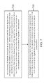
- FIG. 7 is a flowchart for an example method of optimizing latency for a serial transmission.
- FIG. 8 illustrates a system incorporating the SoC and remote processor of FIG. 1 .
- a serial interface serializes a plurality of signals into a frame in which each signal has its own unique position in the frame.
- an eight-bit frame may be considered to be arranged from a first bit through an eighth bit.
- a first signal is defined through the binary value of the first bit
- a second signal is defined through the binary value of the second bit, and so on such that a signal in a received frame may be identified through its position in the frame.
- one or more of the signals may comprise a multi-bit signal. But such multi-bit signals are also assigned to unique positions within a frame.
- a receiver may identify a given signal within the frame by its unique position. For example, the first bit in an frame may be assigned to a first one-bit signal. Similarly, the second bit in a frame may be assigned to second one-bit signal, and so on such that the nth bit in a frame may be assigned to an nth one-bit signal, where n is a positive integer.
- the extension of such unique positioning to multi-bit signals is analogous. For example, an eight-bit signal may be assigned to the first byte of a frame, and so on.
- a serial interface that may be readily modified to practice the latency reduction disclosed herein is a virtual general purpose input output (GPIO) interface such as disclosed in commonly-assigned U.S. application Ser. No. 14/540,366, (the “366 application”) filed Nov. 13, 2014, the contents of which is incorporated by reference.
- GPIO general purpose input output
- any serial interface that transmits serial data in a unique order such as practiced in a universal asynchronous receiver transmitter (UART) interface, a peripheral component interface (PCI), and an inter-integrated circuit (I2C) interface.
- UART universal asynchronous receiver transmitter
- PCI peripheral component interface
- I2C inter-integrated circuit
- An integrated circuit with a VGI interface uses a pair of pins as if they constituted a larger plurality of GPIO pins.
- This architecture is deemed virtual in that, to the system-level applications creating the signals for transmission as virtual GPIO signals through a virtual GPIO interface within the architecture, it is as if the virtual GPIO signals were being transmitted and received on conventional GPIO pins.
- a system on chip (SOC) or processor having a VGI interface thus experiences no functional difference between conventional GPIO signals and virtual GPIO signals. This is advantageous in that the processor needs no new configuration or programming to function with the VGI interface.
- the VGI interface uses only two pins to transmit and receive the virtual GPIO signals that would otherwise each need their own dedicated GPIO pin should they instead be transmitted as conventional GPIO signals.
- a VGI interface makes the health of the transmitting node transparent to the receiving node. This is an important advantage, particularly during the debugging stage for software implementations as it indicates to the receiving processor the time that a transmitting processor became inoperative.
- each processor in the transmitting and receiving integrated circuits communicates through a dedicated transmit pin coupled to a transmit line and a dedicated receive pin coupled to a receive line.
- the transmit line for a transmitting integrated circuit becomes the receive line for a receiving integrated circuit.
- the virtual GPIO signals may be divided into a transmit set for transmission over the transmit line and a receive set for reception on the receive line. If the signaling is symmetric, the number of signals in the transmit set and the receive set for each processor is the same. However, the virtual GPIO architecture disclosed herein can accommodate asymmetric signaling in which the transmit set of virtual GPIO signals for one processor is not the same size as the receive set for the same processor.
- each VGI interface may each receive an external clock signal to synchronize the transmission and reception of VGI frames. But the receipt of an external clock requires a clock pin.
- each VGI interface may include an oversampling clock such as a 16 times (16 ⁇ ) oversampling clock as used in a UART interface.
- each integrated circuit pulse-width modulates its transmit set of virtual GPIO signals into data frames for transmission to another integrated circuit. Each bit in the data frame corresponds to a bit in the transmit set of signals. Control of the pulse width modulation may be performed by a finite state machine (FSM). Each transmitted bit in a data frame is represented by a voltage pulse on the transmit line within a bit period.
- FSM finite state machine
- a first pulse width signifies one binary value for the transmitted bit whereas a second pulse width signifies another binary value for the transmitted bit.
- one pulse width may be more than 50% of the bit period (a majority fraction of the bit period).
- a remaining second pulse width may be less than 50% of the bit period (a minority fraction of the bit period).
- each FSM may include or be associated with an oscillator such as a ring oscillator and one or more counters for counting the oscillations of the oscillator.
- the counter begins counting the number of oscillations prior to the pulsing of the transmit pin/transmit line.
- the counter counts to either a first count or a second count that is greater than the first count.
- the FSM pulses the transmit line.
- each processor may be configured to weakly charge its transmit line to a power supply voltage VDD when idle (no data frames being transmitted).
- each transmit line would be maintained in some default voltage state, which may be referred to as a first binary voltage.
- the start of a transmitted bit would then be identified by charging (or discharging) the transmit line to a second binary voltage.
- the FSM then maintains the transmit line at the second binary voltage for either the majority of the bit period or the minority of the bit period.
- the counter counts to the first count.
- the counter counts to the second count.
- the second binary value is a logical zero whereas the first binary value is a logical one.
- the first binary voltage may equal the power supply voltage VDD whereas the second binary voltage may equal ground.
- the FSM then serially examines each bit in the transmit set and based upon their binary values, either pulses the transmit line with a relatively wide pulse or a relatively narrow pulse for each bit.
- the receiving FSM can then demodulate a received frame of data by determining the pulse widths. This determination may be performed on a bit-by-bit basis by counting the number of oscillations that occur while the receive line is discharged versus the number of oscillations that occur while the receive line is pulsed to the power supply voltage VDD.
- the integrated circuits require no common clock such that the transmission of a frame of data from one integrated circuit is entirely asynchronous with regard to its receipt at a remote integrated circuit. Since there need be no common clock, there is thus no need for a clock pin in each integrated circuit to receive the common clock. This then frees up the pin that might otherwise be preserved for the common clock for other uses.
- FIG. 1 illustrates a VGI architecture 101 that includes an application processor 100 and a modem processor 105 . It will be appreciated, however, that other types of processors may be used within architecture 101 .
- a transmit line 110 a for transmitting virtual GPIO signals as IPC signals from application processor 100 over a transmit pin 111 a is also the receive line for receiving these signals at modem processor 105 on a receive pin 111 b .
- a transmit line 110 b for modem processor 105 for transmitting its IPC signals as virtual GPIO signals is also the receive line for application processor 100 . These lines may be carried on a circuit board between the integrated circuits as indicated by dashed line 150 .
- Each processor includes a transmit pin or pad (not illustrated) to couple to its transmit line. Similarly, each processor includes a receive pin or pad (not illustrated) to couple to its receive line.
- a finite state machine (FSM) 115 in each processor controls the transmission and reception of the virtual GPIO signals using these dedicated lines and pins.
- each processor includes a GPIO interface 103 over which it interfaces with GPIO pins.
- GPIO interface 103 may be unchanged with regard to the corresponding processor in virtual GPIO architecture 101 .
- each processor receives and transmits signals through its GPIO interface 103 in a conventional manner such that virtual GPIO architecture 101 is transparent to processors 100 and 105 .
- a certain portion of the signals processed through each GPIO interface 103 may be transmitted and received on conventional GPIO pins 125 as GPIO signals 130 . But a remaining portion of the signals processed through GPIO interface 103 are not transmitted or received through conventional GPIO pins or pads 125 .
- this remaining portion of the signals processed through GPIO interface 103 comprise a plurality of virtual GPIO signals 135 that are transmitted from FSM 115 over the dedicated transmit pin (or pad) 111 a and received on the dedicated receive pin (or pad) 111 b .
- the portion of the signals received at a GPIO interface 103 from the corresponding processor that are processed as conventional GPIO signals 130 may be denoted herein as a first set of signals.
- the remaining portion of the signals received at a GPIO interface 103 from the corresponding processor that are processed as virtual GPIO signals 135 may be denoted herein as a second set of signals.
- each virtual GPIO signal 135 does have its own dedicated pin but instead is multiplexed with the remaining virtual GPIO signals 135 on pins 111 a and 111 b .
- An integrated circuit such as processor 100 or modem 105 may include just one FSM 115 or may include a plurality of these elements for interfacing with multiple external systems.
- FIG. 2 shows an application processor 220 interfacing with two modem processors 225 and 230 through two FSMs 115 A and 115 B, respectively.
- Each FSM 115 A and 115 B in processor 220 accommodates the virtual GPIO signaling with a corresponding one of the modem processors.
- an integrated circuit such as an SOC may be configured with as many FSMs as is necessary to accommodate virtual GPIO signaling with assorted external processors.
- each FSM communicates using its own dedicated transmit pin 111 a and a dedicated receive pin 111 b as discussed with regard to FIG. 1 .
- virtual GPIO signals 135 are accommodated using a finite state machine such as FSM 115 , the processor cores may be asleep or in other types of dormant states yet be able to receive virtual GPIO signals 135 .
- virtual GPIO architecture 101 not only advantageously economizes the number of pins for each GPIO interface 103 but is also low power.
- pin is a generic term to cover the structure such as a pad or an actual pin that an integrated circuit uses to couple to leads on circuit board or other physical interconnect (e.g., package interconnect or through-hole via interconnect).
- circuit board or other physical interconnect e.g., package interconnect or through-hole via interconnect.
- each integrated circuit has sixteen GPIO pins 125 , then these pins could be configured to accommodate eight symmetric GPIO signals 130 (for illustration clarity, only four conventional GPIO signals #1 through #4 are shown in FIG. 1 ) or sixteen asymmetric GPIO signals 130 .
- each integrated circuit can accommodate the input/output interfacing of a plurality of n virtual GPIO signals 135 using its transmit pin 111 a and receive pin 111 b , wherein n is an arbitrary plural integer.
- each processor core there is no difference between GPIO signals 130 and virtual GPIO signals 135 : they are both simply signals that are transmitted and received as necessary through GPIO interface 103 .
- virtual GPIO signals 135 do not have dedicated pins in contrast to conventional GPIO signals 130
- virtual GPIO signals 135 are serialized in FSMs 115 for transmission on lines 110 a and 110 b .
- each FSM 115 deserializer the received serialized virtual GPIO signals.
- each FSM 115 functions as a serializer/deserializer with regard to virtual GPIO signals 135 .
- each processor may be configured to receive an interrupt signal in response to changes in selected ones of virtual GPIO signals 135 .
- a modem power manager (MPM) 140 monitors the selected virtual GPIO signals as programmed through interrupt (INT_configuration) registers 145 . If MPM 140 sees a monitored signal change, it transmits an interrupt to its processor accordingly.
- each FSM 115 modulates the virtual GPIO signals 135 generated by its processor through the processor's interaction with the corresponding GPIO interface 103 into a pulse-width-modulated signal that is transmitted over transmit line 110 a .
- each FSM 115 receives a pulse-width-modulated signal on its receive line 110 b from a remote processor.
- This pulse transmission is quite advantageous in that it enable asynchronous transmission (no common clock) between processors 100 and 105 as will be explained further herein.
- FIG. 3 is a block diagram of an FSM 115 to better illustrate its transmit and receive operations.
- FSM 115 receives a transmit set of virtual GPIO signals from its GPIO interface 103 (shown in FIG. 1 ) through a multiplexing module 300 .
- This transmit set of virtual GPIO signals would conventionally be transmitted as ordinary GPIO signals 130 discussed with regard to FIG. 1 but are instead identified as virtual GPIO signals 135 by GPIO interface 103 and processed through FSM 115 accordingly.
- FSM 115 includes a logic circuit 301 that will authorize the transmission of the transmit set of virtual GPIO signals as a pulse-width modulated signal over transmit line 110 a if there has been a change in the transmit set as compared to a previous state of the transmit set.
- Logic circuit 301 thus compares the current transmit set of virtual GPIO signals to the previous transmit set stored in a latch or configuration register 107 .
- logic circuit 301 may include an XOR gate 310 that XORs the current transmit set with the previous transmit set stored in configuration register 107 (this previous transmit set may be designated as the “LAST GPIO Status” as shown in FIG. 2 ).
- Multiplexing module 300 loads the current transmit set in parallel into a parallel-in-serial-out (PISO) shift register 315 .
- PISO parallel-in-serial-out
- PISO shift register 315 is then enabled to serially shift out its contents onto transmit line 110 a responsive to a shift signal 120 .
- Each transmit set of virtual GPIO signals 135 from FIG. 1 comprises a frame of data that is stored in PISO shift register 315 .
- FSM 115 includes a pulse-width modulator 355 that pulse-width modulates the transmit set of bits shifted out from PISO shift register 315 into a pulse-width-modulated output signal that is driven to the remote processor on transmit line 110 a .
- This modulation is responsive to counts of oscillation cycles from an oscillator such as the counts of a transmit ring oscillator output signal 360 from a transmit ring oscillator (RO) 350 .
- Modulator 355 and transmit ring oscillator 350 may be triggered by the assertion of enable signal 320 from XOR gate 310 . Responsive to this triggering, modulator 355 strobes shift signal 120 so that PISO shift register 315 shifts an initial bit of the transmit set of virtual GPIO signals to modulator 355 .
- Modulator 355 includes at least one counter (not illustrated) that counts the cycles in ring oscillator output signal 360 . Depending upon the desired pulse width from the pulse width modulation, the counter either counts to a first count or to a second count that is greater than the first count. After counting a sufficient number of cycles to satisfy the appropriate one of the first and second counts, the counter re-strobes shift signal 120 so that a subsequent bit from the frame of data stored in PISO shift register 315 is shifted into modulator 355 . In this fashion, the transmit set of virtual GPIO signals 135 stored as a frame of data in PISO shift register 315 is shifted a bit at a time into modulator 355 .
- pulse-width modulator 355 pulse-width modulates a corresponding pulse transmitted over transmit line 110 a .
- processor 100 may be configured to weakly charge transmit line 110 a high to a power supply voltage VDD during a default state (no data transmission).
- FSM 115 also deserializer a receive set of virtual GPIO signals 135 in an analogous fashion using a serial-in-parallel-out (SIPO) shift register 325 .
- a demodulator 370 demodulates a received pulse-width-modulated signal from a remote processor as received on receive line 110 b .
- Demodulator 370 is configured to detect the start of a received frame of data from the received pulse-width-modulated signal such as by detecting the discharge of receive line 110 b to trigger a receive ring oscillator 375 to begin oscillating a receive ring oscillator output signal 380 .
- ring oscillators 350 and 380 may comprise the same oscillator.
- demodulator 370 may include a counter (not illustrated) such as a low counter and a high counter. In each bit period, the low counter is triggered to count while receive line 110 b is discharged. Conversely, the high counter is triggered to count while receive line 110 b is charged to the power supply voltage VDD. In alternative embodiments, a single common counter may count the number of oscillations in each binary voltage state for receive line 110 b . By comparing the low and high counts, demodulator 370 may form a demodulated data signal 382 accordingly.
- a counter such as a low counter and a high counter. In each bit period, the low counter is triggered to count while receive line 110 b is discharged. Conversely, the high counter is triggered to count while receive line 110 b is charged to the power supply voltage VDD. In alternative embodiments, a single common counter may count the number of oscillations in each binary voltage state for receive line 110 b . By comparing the low and high counts, demodulator 370 may form a demodulated data
- demodulator 370 may drive demodulated data signal 382 high to the power supply voltage VDD to signify that a relatively wide pulse was received. Conversely, if the low count is greater, demodulator 370 may discharge demodulated data signal 382 to VSS to signify that a relatively narrow pulse was received.
- Demodulator 370 may also assert a shift signal 381 to SIPO shift register 325 upon detection from the counts of the bit time period boundaries. SIPO shift register 325 would then shift in demodulated data signal 382 from demodulator 370 . SIPO shift register 325 may provide a complete frame of virtual GPIO data in parallel to an output latch 351 responsive to an output latch strobe signal 390 .
- FSM module 115 may be configured to process a predefined data frame size for the transmit and receive sets of virtual GPIO signals—for example, each set may comprise a plurality n of virtual GPIO signals. The n virtual GPIO signals are transmitted and received in a frame with respect to a start bit and a stop bit.
- FSM 115 is readily programmed to alter this predefined set size as necessary for a given design.
- the start bit is the initial bit in a data frame.
- the stop bit is the final bit in a data frame and may be followed by an additional discharge fraction of the bit period.
- Output latch strobe signal 390 may thus be asserted responsive to detecting that the stop bit has been shifted into SIPO shift register 325 .
- the resulting frame of virtual GPIO data stored in output latch 351 may be presented in parallel to multiplexing module 300 so that it may be transferred to GPIO interface 103 ( FIG. 1 ). Additional details for the pulse width modulation are discussed in the '366 application.
- a conventional GPIO signal is identified through its receipt on a corresponding one of conventional GPIO pins 125 .
- FSM 115 identifies a VGI signal in a VGI frame though its position in the frame. For example, if the payload size for a VGI frame is eight bits arranged from a first bit through a last bit, there would be eight different bit positions in the VGI frame payload. Both the transmitting and receiving FSM 115 may thus be configured with the information of which bit position corresponds to which VGI signal. Given this identify of a VGI signal by its position within the frame, the following latency reduction technique is readily implemented.
- An FSM 115 may be configured as shown in FIG. 4 to include a transmission scheme decision logic circuit 400 and a packet creation logic circuit 405 that together are configured to reduce latency by selecting an appropriate frame type such as a batch-mode frame or a bit-mode frame. It will be appreciated that an analogous FSM may be implemented in any suitable serial interface such as the UART, PCI, and I2C interfaces noted above.
- a memory 410 such as a register stores the previously-transmitted frame. For example, memory 410 may be coupled to multiplexing module 300 to receive the payload for a current frame. This payload is stored in memory 410 and becomes the subsequent payload when a subsequent payload is ready to launched from multiplexing module 300 as the subsequent current frame.
- Transmission scheme decision logic circuit 400 is configured to compare the current payload as received from multiplexing module 300 to the previous payload as received from memory 410 to determine the number of changed bits. Based upon the decision from transmission scheme decision logic circuit 400 , a packet creation circuit 405 forms a packet (frame) based upon the appropriate frame type as selected by transmission scheme decision logic circuit 400 . Packet creation circuit 405 may append a header to the resulting frame to identify the frame type. An I/O transmission circuit 415 (e.g., PISO shift register 315 of FIG. 3 ) may then transmit the selected packet over transmit pin 110 a.
- I/O transmission circuit 415 e.g., PISO shift register 315 of FIG. 3
- transmission scheme decision logic circuit 400 may be better understood with reference to FIG. 5 for an embodiment in which the payload size is eight bits arranged from a VGI signal Q 0 through a bit Q 7 . Each signal has its own corresponding bit position in a frame. In a previous payload 500 , signals Q 7 , Q 3 , Q 2 , and Q 0 were all binary ones whereas signals Q 6 , Q 5 , Q 4 , and Q 1 were binary zeroes. These values remained unchanged in a current payload 505 except for signal Q 6 , which changed to a binary one. Should transmission scheme decision logic circuit 400 ( FIG.
- Batch-mode frame 510 includes a header 520 (which may also be designated as a flag) that identifies batch-mode frame 510 as a batch-mode frame through a binary value of zero.
- header 520 which may also be designated as a flag
- Each bit in batch-mode frame 510 requires a certain amount of time for its transmission, which may be denoted as the bit period. The serial transmission of batch-mode frame 510 would thus require nine bit periods to accommodate all the signals Q 7 through Q 0 as well as header 520 .
- Transmission scheme decision logic circuit 400 compares previous payload 500 to current payload 505 to determine the number of changed signals. Between payloads 500 and 505 , it is only signal Q 6 that has changed (from a binary zero in payload 500 to a binary one in payload 505 ). It will thus reduce latency for transmission scheme decision logic circuit 400 to instead select for a bit-mode frame 515 that merely identifies the bit position of the changed signal (in this case, signal Q 6 ) through an address 525 of the bit position and a binary value 530 of the changed signal.
- a header 520 for bit-mode frame 515 identifies it as a bit-mode frame type by having a binary value of one. It will be appreciated that the actual binary value (and number of bits) of an appropriate header for batch-mode frame 510 and bit-mode frame 515 may be varied in alternative embodiments.
- a receiving FSM 115 ( FIG. 4 ) is configured to analyze header 520 to identify the frame type. If a bit-mode frame type is identified, the receiving FSM 115 assigns the unchanged signals to have the same values as stored in memory 410 .
- Multiplexing module 300 ( FIG. 4 )
- binary value 530 may be omitted from bit-mode frame 515 to further reduce latency in that the receiving FSM may simply invert the stored value of the signal identified by address 525 to recover binary value 530 .
- the threshold used by transmission scheme decision logic circuit 400 with regard to the number of changed signals 530 will depend upon the payload size.
- a bit-mode frame type will not reduce latency as each changed bit requires 3 address bits to identify its bit position and potentially another bit to identify the changed binary value.
- Transmission scheme decision logic circuit 400 may thus be configured in a byte payload embodiment to select for a batch-mode frame type if more than one bit has changed in current payload 505 . But the threshold changes if the payload size increases. For example, a payload 600 of two bytes is shown in FIG. 6 .
- a header 605 may comprises two bits.
- a full-batch mode 610 includes entire payload 600 . With the combination of payload 600 , full-batch mode 610 thus requires eighteen bit periods for its serial transmission such that the latency reduction compared to the original payload latency of sixteen bit periods is ⁇ 12.5%. Full-batch mode 610 is favored if each byte in payload 600 has one or more changed bits.
- a byte-mode frame 615 is favored in which the changed byte is transmitted in a byte-mode of transmission.
- Byte-mode frame 615 includes a byte number flag 635 to identify which byte is being transmitted in full. The receiving FSM 115 ( FIG. 4 ) would then assign the unchanged byte to have the values for that byte stored in memory 410 .
- Byte-mode frame 615 uses eleven bit periods for its serial transmission such that the latency reduction with regard to payload 600 is 31.25%.
- a bit-mode frame 620 is favored if only one bit in one of the bytes in payload 600 has changed.
- a binary value 630 for the changed bit is optional in that the stored value at the corresponding bit position in memory 410 may simply be inverted to recover binary value 630 as discussed analogously with regard to bit-mode frame 515 .
- Byte-mode frame 615 may readily be extended to larger payloads by modifying byte number 635 accordingly.
- the method includes an act 700 for a plurality of signals arranged in a payload such that each signal has a corresponding bit position in the payload.
- An example of such a payload includes payload 500 and 505 of FIG. 5 and payload 600 of FIG. 6 .
- Act 700 includes serially transmitting a first frame that identifies the bit position of a changed one of the signals in the payload responsive to a determination that only the changed one of the signals has changed state since the first frame transmission, wherein the first frame does not includes an unchanged remainder of the plurality of signals in the payload.
- An example of such a first frame transmission is discussed above with regard to bit-mode frame 515 of FIG. 5 or bit-mode frame 620 of FIG. 6 .
- the method includes an act 705 that occurs subsequent to the second frame transmission and comprises transmitting a second frame including the plurality of signals in the payload responsive to a determination that more than one of the signals has changed state since the first frame transmission.
- An example of the second frame transmission is discussed above with regard to batch-mode frame 510 of FIG. 5 and batch-mode frame 610 of FIG. 6 .
- FIG. 8 An example system 800 is shown in FIG. 8 in which a system-on-a-chip (SOC) 805 is configured with an FSM (not illustrated) such as FSM 115 discussed above for optimizing the latency of serial communication with a plurality of peripheral devices 810 .
- SOC system-on-a-chip
- Each peripheral device 810 thus also includes a corresponding FSM as well.
- the corresponding two-wire link between SOC 805 and each peripheral device 810 is also not shown for illustration clarity but contained within a system bus 815 .
- System 800 may comprise a cellular phone, smart phone, personal digital assistant, tablet computer, laptop computer, digital camera, handheld gaming device, or other suitable device.
- SoC 805 In addition to communicating with peripheral devices 810 , SoC 805 also communicates through system bus 815 with a memory such as a DRAM 820 and a display controller 825 .
- Display controller 825 in turn couples to a video processor 830 that drives a display 835 .
- FSM 115 may be readily modified to implement the disclosed latency reduction for any suitable serial interface such as UART, PCI, I2C, and so on.
- any suitable serial interface such as UART, PCI, I2C, and so on.
Landscapes
- Engineering & Computer Science (AREA)
- Theoretical Computer Science (AREA)
- General Engineering & Computer Science (AREA)
- Physics & Mathematics (AREA)
- General Physics & Mathematics (AREA)
- Computer Hardware Design (AREA)
- Microelectronics & Electronic Packaging (AREA)
- Signal Processing (AREA)
- Computing Systems (AREA)
- Information Transfer Systems (AREA)
Priority Applications (4)
| Application Number | Priority Date | Filing Date | Title |
|---|---|---|---|
| US15/040,271 US9934171B2 (en) | 2016-02-10 | 2016-02-10 | Serial communication link with optimal transfer latency |
| PCT/US2017/012874 WO2017139059A1 (fr) | 2016-02-10 | 2017-01-10 | Liaison de communication série à latence de transfert optimale |
| CN201780010219.1A CN108604219B (zh) | 2016-02-10 | 2017-01-10 | 具有最优传输等待时间的串行通信链路 |
| EP17702195.3A EP3387546B1 (fr) | 2016-02-10 | 2017-01-10 | Liaison de communication série à latence de transfert optimale |
Applications Claiming Priority (1)
| Application Number | Priority Date | Filing Date | Title |
|---|---|---|---|
| US15/040,271 US9934171B2 (en) | 2016-02-10 | 2016-02-10 | Serial communication link with optimal transfer latency |
Publications (2)
| Publication Number | Publication Date |
|---|---|
| US20170228327A1 US20170228327A1 (en) | 2017-08-10 |
| US9934171B2 true US9934171B2 (en) | 2018-04-03 |
Family
ID=57915097
Family Applications (1)
| Application Number | Title | Priority Date | Filing Date |
|---|---|---|---|
| US15/040,271 Active 2036-11-03 US9934171B2 (en) | 2016-02-10 | 2016-02-10 | Serial communication link with optimal transfer latency |
Country Status (4)
| Country | Link |
|---|---|
| US (1) | US9934171B2 (fr) |
| EP (1) | EP3387546B1 (fr) |
| CN (1) | CN108604219B (fr) |
| WO (1) | WO2017139059A1 (fr) |
Cited By (1)
| Publication number | Priority date | Publication date | Assignee | Title |
|---|---|---|---|---|
| US11436176B2 (en) | 2019-01-25 | 2022-09-06 | Samsung Electronics Co., Ltd. | Semiconductor integrated circuit and operation method thereof |
Families Citing this family (7)
| Publication number | Priority date | Publication date | Assignee | Title |
|---|---|---|---|---|
| EP3507672B1 (fr) * | 2016-09-05 | 2024-07-03 | IOT.nxt BV | Système et procédé d'interface de dispositif définie par un logiciel |
| US10343606B2 (en) * | 2017-05-05 | 2019-07-09 | Connaught Electronics Ltd. | Using parallel data lines for GPIO purposes |
| US10073799B1 (en) * | 2017-11-02 | 2018-09-11 | Synopsys, Inc. | Programmable data width converter device, system and method thereof |
| US11943658B2 (en) * | 2020-11-03 | 2024-03-26 | Cypress Semiconductor Corporation | Multi-protocol communication network |
| US11960434B2 (en) * | 2021-04-07 | 2024-04-16 | Sony Semiconductor Solutions Corporation | Communication device, communication system, and communication method for transmitting data blocks including signal groups conforming to a serial peripheral interface |
| US11921651B2 (en) * | 2021-06-07 | 2024-03-05 | AyDeeKay LLC | Interface module with low-latency communication of electrical signals between power domains |
| US11757610B1 (en) * | 2022-04-18 | 2023-09-12 | Nxp B.V. | Low phase noise clock recovery over a data connection |
Citations (10)
| Publication number | Priority date | Publication date | Assignee | Title |
|---|---|---|---|---|
| US6791358B2 (en) | 2002-04-16 | 2004-09-14 | Infineon Technologies Ag | Circuit configuration with signal lines for serially transmitting a plurality of bit groups |
| US20060143348A1 (en) * | 2004-12-29 | 2006-06-29 | Wilson Matthew T | System, method, and apparatus for extended serial peripheral interface |
| US20100115140A1 (en) | 2008-10-30 | 2010-05-06 | Micron Technology, Inc. | Encoded addressing within control code for bus communication |
| EP2330514A1 (fr) | 2009-12-07 | 2011-06-08 | STMicroelectronics (Research & Development) Limited | Paquet de circuits intégrés |
| US8027359B2 (en) | 2007-03-26 | 2011-09-27 | Sony Corporation | Extended serial communication protocols |
| US20130166800A1 (en) | 2010-06-23 | 2013-06-27 | Carsten Bosse | Method and device for transmitting data having a variable bit length |
| US8606982B2 (en) | 2008-03-10 | 2013-12-10 | Qimonda Ag | Derivative logical output |
| US8989328B2 (en) | 2013-03-14 | 2015-03-24 | Qualcomm Incorporated | Systems and methods for serial communication |
| WO2015077803A1 (fr) | 2013-11-22 | 2015-05-28 | Qualcomm Incorporated | Gpio virtuelle sans horloge |
| US20160224489A1 (en) * | 2015-02-04 | 2016-08-04 | Qualcomm Incorporated | Voltage mode and current mode device enumeration |
Family Cites Families (2)
| Publication number | Priority date | Publication date | Assignee | Title |
|---|---|---|---|---|
| KR100711738B1 (ko) * | 2005-02-15 | 2007-04-25 | 삼성전자주식회사 | 비트맵 기반 자동 재전송 요구 엔진 및 그것의 제어 방법 |
| EP2232786A1 (fr) * | 2007-12-20 | 2010-09-29 | BRITISH TELECOMMUNICATIONS public limited company | Plan d'adaptation client-serveur pour un trafic de communication |
-
2016
- 2016-02-10 US US15/040,271 patent/US9934171B2/en active Active
-
2017
- 2017-01-10 EP EP17702195.3A patent/EP3387546B1/fr active Active
- 2017-01-10 CN CN201780010219.1A patent/CN108604219B/zh active Active
- 2017-01-10 WO PCT/US2017/012874 patent/WO2017139059A1/fr active Application Filing
Patent Citations (10)
| Publication number | Priority date | Publication date | Assignee | Title |
|---|---|---|---|---|
| US6791358B2 (en) | 2002-04-16 | 2004-09-14 | Infineon Technologies Ag | Circuit configuration with signal lines for serially transmitting a plurality of bit groups |
| US20060143348A1 (en) * | 2004-12-29 | 2006-06-29 | Wilson Matthew T | System, method, and apparatus for extended serial peripheral interface |
| US8027359B2 (en) | 2007-03-26 | 2011-09-27 | Sony Corporation | Extended serial communication protocols |
| US8606982B2 (en) | 2008-03-10 | 2013-12-10 | Qimonda Ag | Derivative logical output |
| US20100115140A1 (en) | 2008-10-30 | 2010-05-06 | Micron Technology, Inc. | Encoded addressing within control code for bus communication |
| EP2330514A1 (fr) | 2009-12-07 | 2011-06-08 | STMicroelectronics (Research & Development) Limited | Paquet de circuits intégrés |
| US20130166800A1 (en) | 2010-06-23 | 2013-06-27 | Carsten Bosse | Method and device for transmitting data having a variable bit length |
| US8989328B2 (en) | 2013-03-14 | 2015-03-24 | Qualcomm Incorporated | Systems and methods for serial communication |
| WO2015077803A1 (fr) | 2013-11-22 | 2015-05-28 | Qualcomm Incorporated | Gpio virtuelle sans horloge |
| US20160224489A1 (en) * | 2015-02-04 | 2016-08-04 | Qualcomm Incorporated | Voltage mode and current mode device enumeration |
Non-Patent Citations (2)
| Title |
|---|
| International Search Report and Written Opinion-PCT/US2017/012874-ISA/EPO-dated May 10, 2017. |
| International Search Report and Written Opinion—PCT/US2017/012874—ISA/EPO—dated May 10, 2017. |
Cited By (1)
| Publication number | Priority date | Publication date | Assignee | Title |
|---|---|---|---|---|
| US11436176B2 (en) | 2019-01-25 | 2022-09-06 | Samsung Electronics Co., Ltd. | Semiconductor integrated circuit and operation method thereof |
Also Published As
| Publication number | Publication date |
|---|---|
| CN108604219A (zh) | 2018-09-28 |
| EP3387546B1 (fr) | 2019-10-16 |
| EP3387546A1 (fr) | 2018-10-17 |
| WO2017139059A1 (fr) | 2017-08-17 |
| US20170228327A1 (en) | 2017-08-10 |
| CN108604219B (zh) | 2021-05-04 |
Similar Documents
| Publication | Publication Date | Title |
|---|---|---|
| US9934171B2 (en) | Serial communication link with optimal transfer latency | |
| US9619427B2 (en) | Hybrid virtual GPIO | |
| US10241953B2 (en) | Dynamic data-link selection over common physical interface | |
| US9582456B2 (en) | Virtual GPIO | |
| US10303643B2 (en) | Enhanced virtual GPIO with multi-mode modulation | |
| US9880965B2 (en) | Variable frame length virtual GPIO with a modified UART interface | |
| KR102328014B1 (ko) | 싱글 와이어 인터페이스를 포함하는 장치와 이를 포함하는 데이터 처리 시스템 | |
| KR101823315B1 (ko) | 가변 프레임 길이를 갖는 2-와이어 인터페이스 시스템에 대한 임피던스-기반 플로우 제어 | |
| US9747244B2 (en) | Clockless virtual GPIO | |
| EP3117330A1 (fr) | Gpio virtuelle sans horloge |
Legal Events
| Date | Code | Title | Description |
|---|---|---|---|
| AS | Assignment |
Owner name: QUALCOMM INCORPORATED, CALIFORNIA Free format text: ASSIGNMENT OF ASSIGNORS INTEREST;ASSIGNORS:MISHRA, LALAN JEE;WIETFELDT, RICHARD;SIGNING DATES FROM 20160713 TO 20161208;REEL/FRAME:041114/0963 |
|
| STCF | Information on status: patent grant |
Free format text: PATENTED CASE |
|
| MAFP | Maintenance fee payment |
Free format text: PAYMENT OF MAINTENANCE FEE, 4TH YEAR, LARGE ENTITY (ORIGINAL EVENT CODE: M1551); ENTITY STATUS OF PATENT OWNER: LARGE ENTITY Year of fee payment: 4 |