US9929068B2 - Film-like wafer mold material, molded wafer, and semiconductor device - Google Patents
Film-like wafer mold material, molded wafer, and semiconductor device Download PDFInfo
- Publication number
- US9929068B2 US9929068B2 US13/410,887 US201213410887A US9929068B2 US 9929068 B2 US9929068 B2 US 9929068B2 US 201213410887 A US201213410887 A US 201213410887A US 9929068 B2 US9929068 B2 US 9929068B2
- Authority
- US
- United States
- Prior art keywords
- film layer
- wafer
- film
- mold material
- filler
- Prior art date
- Legal status (The legal status is an assumption and is not a legal conclusion. Google has not performed a legal analysis and makes no representation as to the accuracy of the status listed.)
- Active, expires
Links
- PTXDNOIAVRKJJR-UHFFFAOYSA-N CC(C)(C(F)(F)F)C(F)(F)F.CC(C)(C)C.CC1(C)C2=C(C=CC=C2)C2=C/C=C/C=C\21.CCC Chemical compound CC(C)(C(F)(F)F)C(F)(F)F.CC(C)(C)C.CC1(C)C2=C(C=CC=C2)C2=C/C=C/C=C\21.CCC PTXDNOIAVRKJJR-UHFFFAOYSA-N 0.000 description 6
- 0 C.C.C.C.C.C.C.C.C.C.C.C.C.C.C.C.CCC[Si](C)(C)C1=CC=C([Si](C)(C)CC)C=C1.CC[Si](C)(C)C1=CC=C([Si](C)(C)C[Y]C)C=C1.[1*][Si]([2*])(CC)O[Si]([3*])([4*])CCC.[1*][Si]([2*])(CC)O[Si]([3*])([4*])C[Y]C Chemical compound C.C.C.C.C.C.C.C.C.C.C.C.C.C.C.C.CCC[Si](C)(C)C1=CC=C([Si](C)(C)CC)C=C1.CC[Si](C)(C)C1=CC=C([Si](C)(C)C[Y]C)C=C1.[1*][Si]([2*])(CC)O[Si]([3*])([4*])CCC.[1*][Si]([2*])(CC)O[Si]([3*])([4*])C[Y]C 0.000 description 4
- ZCQGIEIHTMYXCU-UHFFFAOYSA-N C1=CC=C(OCC2CC2)C=C1.C1=CC=C(OCC2CO2)C=C1.CC.CC.CC.CC.CCC Chemical compound C1=CC=C(OCC2CC2)C=C1.C1=CC=C(OCC2CO2)C=C1.CC.CC.CC.CC.CCC ZCQGIEIHTMYXCU-UHFFFAOYSA-N 0.000 description 3
- UQVBVETZOBGEHQ-UHFFFAOYSA-N CC.CC.CC.CC.CCC.OC1=CC=CC=C1.OC1=CC=CC=C1 Chemical compound CC.CC.CC.CC.CCC.OC1=CC=CC=C1.OC1=CC=CC=C1 UQVBVETZOBGEHQ-UHFFFAOYSA-N 0.000 description 3
- JGEOHWFESBJHEJ-UHFFFAOYSA-N C1=CC=C(OCC2CO2)C=C1.C1=CC=C(OCC2CO2)C=C1.C=CCC.C=CCC.CC.CC.CCC Chemical compound C1=CC=C(OCC2CO2)C=C1.C1=CC=C(OCC2CO2)C=C1.C=CCC.C=CCC.CC.CC.CCC JGEOHWFESBJHEJ-UHFFFAOYSA-N 0.000 description 1
- VTCOVBGBLLEXJU-UHFFFAOYSA-N C=CCC.C=CCC.CC.CC.CCC.OC1=CC=CC=C1.OC1=CC=CC=C1 Chemical compound C=CCC.C=CCC.CC.CC.CCC.OC1=CC=CC=C1.OC1=CC=CC=C1 VTCOVBGBLLEXJU-UHFFFAOYSA-N 0.000 description 1
- JJLXCRSDCSHWRT-UHFFFAOYSA-N C=CCC1=CC(C(C)(C)C2=CC(CC=C)=C(OCC3CO3)C=C2)=CC=C1OCC1CO1.C=CCC1=CC(C2(C3=CC(CC=C)=C(O)C=C3)C3=C(C=CC=C3)C3=C\C=C/C=C\32)=CC=C1O.[H][Si](C)(C)C1=CC=C([Si]([H])(C)C)C=C1.[H][Si](C)(C)O[Si](C)(C)O[Si](C)(C)O[Si](C)(C)O[Si](C)(C)O[Si](C)(C)O[Si](C)(C)O[Si](C)(C)O[Si](C)(C)O[Si](C)(C)O[Si](C)(C)O[Si](C)(C)O[Si](C)(C)O[Si](C)(C)O[Si](C)(C)O[Si](C)(C)O[Si](C)(C)O[Si](C)(C)O[Si](C)(C)O[Si](C)(C)O[Si](C)(C)O[Si](C)(C)O[Si](C)(C)O[Si](C)(C)O[Si](C)(C)O[Si](C)(C)O[Si](C)(C)O[Si](C)(C)O[Si](C)(C)O[Si](C)(C)O[Si](C)(C)O[Si](C)(C)O[Si](C)(C)O[Si](C)(C)O[Si](C)(C)O[Si](C)(C)O[Si](C)(C)O[Si](C)(C)O[Si](C)(C)O[Si](C)(C)O[Si]([H])(C)C.[H][Si](C)(C)O[Si]([H])(C)C Chemical compound C=CCC1=CC(C(C)(C)C2=CC(CC=C)=C(OCC3CO3)C=C2)=CC=C1OCC1CO1.C=CCC1=CC(C2(C3=CC(CC=C)=C(O)C=C3)C3=C(C=CC=C3)C3=C\C=C/C=C\32)=CC=C1O.[H][Si](C)(C)C1=CC=C([Si]([H])(C)C)C=C1.[H][Si](C)(C)O[Si](C)(C)O[Si](C)(C)O[Si](C)(C)O[Si](C)(C)O[Si](C)(C)O[Si](C)(C)O[Si](C)(C)O[Si](C)(C)O[Si](C)(C)O[Si](C)(C)O[Si](C)(C)O[Si](C)(C)O[Si](C)(C)O[Si](C)(C)O[Si](C)(C)O[Si](C)(C)O[Si](C)(C)O[Si](C)(C)O[Si](C)(C)O[Si](C)(C)O[Si](C)(C)O[Si](C)(C)O[Si](C)(C)O[Si](C)(C)O[Si](C)(C)O[Si](C)(C)O[Si](C)(C)O[Si](C)(C)O[Si](C)(C)O[Si](C)(C)O[Si](C)(C)O[Si](C)(C)O[Si](C)(C)O[Si](C)(C)O[Si](C)(C)O[Si](C)(C)O[Si](C)(C)O[Si](C)(C)O[Si](C)(C)O[Si]([H])(C)C.[H][Si](C)(C)O[Si]([H])(C)C JJLXCRSDCSHWRT-UHFFFAOYSA-N 0.000 description 1
- KQERVIARWMHFOS-UHFFFAOYSA-N [H][Si](C)(C)C1=CC=C([Si]([H])(C)C)C=C1 Chemical compound [H][Si](C)(C)C1=CC=C([Si]([H])(C)C)C=C1 KQERVIARWMHFOS-UHFFFAOYSA-N 0.000 description 1
Classifications
-
- H01L23/295—
-
- H—ELECTRICITY
- H10—SEMICONDUCTOR DEVICES; ELECTRIC SOLID-STATE DEVICES NOT OTHERWISE PROVIDED FOR
- H10W—GENERIC PACKAGES, INTERCONNECTIONS, CONNECTORS OR OTHER CONSTRUCTIONAL DETAILS OF DEVICES COVERED BY CLASS H10
- H10W74/00—Encapsulations, e.g. protective coatings
- H10W74/40—Encapsulations, e.g. protective coatings characterised by their materials
- H10W74/47—Encapsulations, e.g. protective coatings characterised by their materials comprising organic materials, e.g. plastics or resins
- H10W74/473—Encapsulations, e.g. protective coatings characterised by their materials comprising organic materials, e.g. plastics or resins containing a filler
-
- C—CHEMISTRY; METALLURGY
- C08—ORGANIC MACROMOLECULAR COMPOUNDS; THEIR PREPARATION OR CHEMICAL WORKING-UP; COMPOSITIONS BASED THEREON
- C08G—MACROMOLECULAR COMPOUNDS OBTAINED OTHERWISE THAN BY REACTIONS ONLY INVOLVING UNSATURATED CARBON-TO-CARBON BONDS
- C08G59/00—Polycondensates containing more than one epoxy group per molecule; Macromolecules obtained by polymerising compounds containing more than one epoxy group per molecule using curing agents or catalysts which react with the epoxy groups
- C08G59/18—Macromolecules obtained by polymerising compounds containing more than one epoxy group per molecule using curing agents or catalysts which react with the epoxy groups ; e.g. general methods of curing
- C08G59/40—Macromolecules obtained by polymerising compounds containing more than one epoxy group per molecule using curing agents or catalysts which react with the epoxy groups ; e.g. general methods of curing characterised by the curing agents used
- C08G59/4007—Curing agents not provided for by the groups C08G59/42 - C08G59/66
- C08G59/4014—Nitrogen containing compounds
- C08G59/4042—Imines; Imides
-
- C—CHEMISTRY; METALLURGY
- C08—ORGANIC MACROMOLECULAR COMPOUNDS; THEIR PREPARATION OR CHEMICAL WORKING-UP; COMPOSITIONS BASED THEREON
- C08G—MACROMOLECULAR COMPOUNDS OBTAINED OTHERWISE THAN BY REACTIONS ONLY INVOLVING UNSATURATED CARBON-TO-CARBON BONDS
- C08G59/00—Polycondensates containing more than one epoxy group per molecule; Macromolecules obtained by polymerising compounds containing more than one epoxy group per molecule using curing agents or catalysts which react with the epoxy groups
- C08G59/18—Macromolecules obtained by polymerising compounds containing more than one epoxy group per molecule using curing agents or catalysts which react with the epoxy groups ; e.g. general methods of curing
- C08G59/40—Macromolecules obtained by polymerising compounds containing more than one epoxy group per molecule using curing agents or catalysts which react with the epoxy groups ; e.g. general methods of curing characterised by the curing agents used
- C08G59/4007—Curing agents not provided for by the groups C08G59/42 - C08G59/66
- C08G59/4085—Curing agents not provided for by the groups C08G59/42 - C08G59/66 silicon containing compounds
-
- C—CHEMISTRY; METALLURGY
- C08—ORGANIC MACROMOLECULAR COMPOUNDS; THEIR PREPARATION OR CHEMICAL WORKING-UP; COMPOSITIONS BASED THEREON
- C08G—MACROMOLECULAR COMPOUNDS OBTAINED OTHERWISE THAN BY REACTIONS ONLY INVOLVING UNSATURATED CARBON-TO-CARBON BONDS
- C08G77/00—Macromolecular compounds obtained by reactions forming a linkage containing silicon with or without sulfur, nitrogen, oxygen or carbon in the main chain of the macromolecule
- C08G77/48—Macromolecular compounds obtained by reactions forming a linkage containing silicon with or without sulfur, nitrogen, oxygen or carbon in the main chain of the macromolecule in which at least two but not all the silicon atoms are connected by linkages other than oxygen atoms
- C08G77/50—Macromolecular compounds obtained by reactions forming a linkage containing silicon with or without sulfur, nitrogen, oxygen or carbon in the main chain of the macromolecule in which at least two but not all the silicon atoms are connected by linkages other than oxygen atoms by carbon linkages
- C08G77/52—Macromolecular compounds obtained by reactions forming a linkage containing silicon with or without sulfur, nitrogen, oxygen or carbon in the main chain of the macromolecule in which at least two but not all the silicon atoms are connected by linkages other than oxygen atoms by carbon linkages containing aromatic rings
-
- C—CHEMISTRY; METALLURGY
- C09—DYES; PAINTS; POLISHES; NATURAL RESINS; ADHESIVES; COMPOSITIONS NOT OTHERWISE PROVIDED FOR; APPLICATIONS OF MATERIALS NOT OTHERWISE PROVIDED FOR
- C09D—COATING COMPOSITIONS, e.g. PAINTS, VARNISHES OR LACQUERS; FILLING PASTES; CHEMICAL PAINT OR INK REMOVERS; INKS; CORRECTING FLUIDS; WOODSTAINS; PASTES OR SOLIDS FOR COLOURING OR PRINTING; USE OF MATERIALS THEREFOR
- C09D183/00—Coating compositions based on macromolecular compounds obtained by reactions forming in the main chain of the macromolecule a linkage containing silicon, with or without sulfur, nitrogen, oxygen, or carbon only; Coating compositions based on derivatives of such polymers
- C09D183/14—Coating compositions based on macromolecular compounds obtained by reactions forming in the main chain of the macromolecule a linkage containing silicon, with or without sulfur, nitrogen, oxygen, or carbon only; Coating compositions based on derivatives of such polymers in which at least two but not all the silicon atoms are connected by linkages other than oxygen atoms
-
- H01L23/296—
-
- H—ELECTRICITY
- H10—SEMICONDUCTOR DEVICES; ELECTRIC SOLID-STATE DEVICES NOT OTHERWISE PROVIDED FOR
- H10W—GENERIC PACKAGES, INTERCONNECTIONS, CONNECTORS OR OTHER CONSTRUCTIONAL DETAILS OF DEVICES COVERED BY CLASS H10
- H10W74/00—Encapsulations, e.g. protective coatings
- H10W74/40—Encapsulations, e.g. protective coatings characterised by their materials
- H10W74/47—Encapsulations, e.g. protective coatings characterised by their materials comprising organic materials, e.g. plastics or resins
- H10W74/476—Organic materials comprising silicon
-
- C—CHEMISTRY; METALLURGY
- C08—ORGANIC MACROMOLECULAR COMPOUNDS; THEIR PREPARATION OR CHEMICAL WORKING-UP; COMPOSITIONS BASED THEREON
- C08K—Use of inorganic or non-macromolecular organic substances as compounding ingredients
- C08K3/00—Use of inorganic substances as compounding ingredients
- C08K3/34—Silicon-containing compounds
- C08K3/36—Silica
-
- C—CHEMISTRY; METALLURGY
- C08—ORGANIC MACROMOLECULAR COMPOUNDS; THEIR PREPARATION OR CHEMICAL WORKING-UP; COMPOSITIONS BASED THEREON
- C08L—COMPOSITIONS OF MACROMOLECULAR COMPOUNDS
- C08L63/00—Compositions of epoxy resins; Compositions of derivatives of epoxy resins
-
- H01L2924/00—
-
- H01L2924/0002—
-
- Y—GENERAL TAGGING OF NEW TECHNOLOGICAL DEVELOPMENTS; GENERAL TAGGING OF CROSS-SECTIONAL TECHNOLOGIES SPANNING OVER SEVERAL SECTIONS OF THE IPC; TECHNICAL SUBJECTS COVERED BY FORMER USPC CROSS-REFERENCE ART COLLECTIONS [XRACs] AND DIGESTS
- Y10—TECHNICAL SUBJECTS COVERED BY FORMER USPC
- Y10T—TECHNICAL SUBJECTS COVERED BY FORMER US CLASSIFICATION
- Y10T428/00—Stock material or miscellaneous articles
- Y10T428/31504—Composite [nonstructural laminate]
- Y10T428/31511—Of epoxy ether
-
- Y—GENERAL TAGGING OF NEW TECHNOLOGICAL DEVELOPMENTS; GENERAL TAGGING OF CROSS-SECTIONAL TECHNOLOGIES SPANNING OVER SEVERAL SECTIONS OF THE IPC; TECHNICAL SUBJECTS COVERED BY FORMER USPC CROSS-REFERENCE ART COLLECTIONS [XRACs] AND DIGESTS
- Y10—TECHNICAL SUBJECTS COVERED BY FORMER USPC
- Y10T—TECHNICAL SUBJECTS COVERED BY FORMER US CLASSIFICATION
- Y10T428/00—Stock material or miscellaneous articles
- Y10T428/31504—Composite [nonstructural laminate]
- Y10T428/31652—Of asbestos
- Y10T428/31663—As siloxane, silicone or silane
Definitions
- the present invention relates to a film-like wafer mold material used for molding a wafer in a lump.
- a technology for sealing in a wafer level is demanded, with increasing in diameter and reducing in film thickness of a size of a wafer for use in manufacture of a semiconductor device in recent years. Therefore, besides a conventional transfer molding method using a solid type epoxy resin, a compression molding method using a liquid type epoxy resin has been suggested (Patent Publication No. WO2009-142065). However, in the transfer molding, there is concern that wire deformation may occur since a resin is flowed in a narrow portion, and there arises a problem that a filling failure is also apt to occur due to an increase in a sealing area.
- the compression molding method has a problem that fine control in the molding range at an end face portion of a wafer is difficult and optimizing liquidity and physical properties when pouring a liquid sealing resin into a molding machine is not easy. Furthermore, warp of a molded wafer, which has been unquestioned, becomes an issue due to an increase in diameter of a wafer size and a reduction in film thickness of a wafer in recent years, and excellent wafer protection performance is demanded. Therefore, there is demanded development of a wafer mold material that enables molding a wafer in a lump without causing problems such as a filling failure on a wafer surface and has low-warp properties and good wafer protection performance after molding.
- the present invention has been accomplished in view of the above-described problems, and provides a film-like wafer mold material that does not has a liquid form but a film form, enables molding a wafer in a lump (wafer molding), and has good transference performance with respect to a thin-film wafer with a large diameter in particular, good filling properties for a wafer surface before molding, and low-warp properties and good wafer protection performance after molding, and can be preferably used for a wafer level package.
- a film-like wafer mold material for molding a wafer in a lump comprising:
- a multilayer structure constituted of at least a first film layer and a second film layer provided on the first film layer
- the first film layer contains a silicone-backbone-containing polymer, a cross-linking agent, and a filler
- the second film layer contains a silicone-backbone-containing polymer and a cross-linking agent, and further contains a filler in such a manner that a content rate of the filler becomes 0 or above and less than 100 when a content rate of the filler contained in the first film layer is assumed to be 100.
- the material When such a wafer mold material is provided, the material enables molding a wafer in a lump (wafer molding) and has good transference performance with respect to a thin-film wafer having a large diameter since the material has a film-like form. Additionally, since the film-like wafer mold material has the multilayer structure including two types of films that are different in performance, i.e., the first film layer which is of a high-filler type superior in low-warp properties and wafer protection properties and the second film layer which is of a low-filler type that has good filling properties with respect to a wafer surface and enables molding a wafer in a lump, this material can be used as the film-like wafer mold material that has excellent wafer surface filling properties before molding and has low-warp properties and excellent wafer protection performance after molding, and it can be preferably used in a wafer-level package.
- the first film layer is an outermost layer when the wafer is molded in a lump.
- the film-like wafer mold material that can excellently realize the wafer protection properties can be provided, which is preferable.
- a thickness of the film-like wafer mold material is 700 ⁇ m or below.
- the film-like wafer mold material which is further superior in low-warp properties, can be provided, which is preferable.
- the cross-linking agent prefferably be an epoxy compound.
- the first film layer can have further excellent low-warp properties and wafer protection properties, and the second film layer can have the further excellent wafer surface filling properties, which is preferable.
- the silicone-backbone-containing polymer has a repeating unit represented by the following general formula (1) and has a weight average molecular weight of 3,000 to 500,000,
- Z represents a bivalent organic group selected from the following chemical structures
- each of R 5 or R 6 represents an alkyl group or an alkoxy group having a carbon number from 1 to 4, and may be the same or different; k represents any one of 0, 1, and 2,
- V represents a bivalent organic group selected from the following chemical structures
- each of R 7 and R 8 represents an alkyl group or an alkoxy group having a carbon number from 1 to 4, and may be the same or different; h represents any one of 0, 1, and 2.
- the first film layer has the further excellent low-warp properties and wafer protection properties
- the second film layer has the further excellent wafer surface filling properties, which is preferable.
- a wafer molded in a lump with the film-like wafer mold material there is provided a wafer molded in a lump with the film-like wafer mold material.
- the wafer that is less warped and sufficiently protected can be provided.
- the wafer is molded in a lump with the first film layer in the film-like wafer mold material being an outermost layer.
- the wafer that can realize the good wafer protection properties and is protected in a further excellent manner can be provided, which is preferable.
- a semiconductor device obtained by dividing the wafer into individual pieces.
- the semiconductor device obtained by dividing the wafer that is less warped and sufficiently protected into individual pieces can be a high-quality semiconductor device having an excellent yield ratio.
- the material when a film-like wafer mold material according to the present invention is provided, the material enables molding a wafer in a lump and has good transference performance with respect to a thin-film wafer having a large diameter since the material has a film-like form.
- the film-like wafer mold material has the multilayer structure including two types of films that are different in performance, i.e., the first film layer which is of a high-filler type superior in low-warp properties and wafer protection properties and the second film layer which is of a low-filler type that has good filling properties with respect to a wafer surface and enables molding a wafer in a lump, and hence this material can be used as the film-like wafer mold material that has excellent wafer surface filling properties before molding and has low-warp properties and excellent wafer protection performance after molding, and can be preferably used for a wafer-level package.
- the present invention it is possible to provide the wafer that is less warped and sufficiently protected by molding using the film-like wafer mold material and also the high-quality semiconductor device having a good yield ratio that can be obtained by dividing the wafer that is less warped and sufficiently protected into respective pieces.
- a wafer mold material superior in low-warp properties and wafer protection properties can be provided as a filler filling ratio is increased and a wafer mold material superior in filling properties with respect to a wafer surface for molding a wafer in a lump can be provided as the filler filling ratio is decreased, and found out that the wafer mold material having functions of two film layers at the same time can be provided by containing a multilayer structure including two types of film layers different in performance, i.e., the first film layer which is of a high-filler type and the second film layer which is of a low-filler type, thereby bringing the present invention to completion.
- the present invention will now be described hereinafter in detail.
- the present invention provides a film-like wafer mold material for molding a wafer in a lump, comprising:
- a multilayer structure constituted of at least the first film layer and the second film layer provided on the first film layer
- the first film layer contains a silicone-backbone-containing polymer, a cross-linking agent, and a filler
- the second film layer contains a silicone-backbone-containing polymer and a cross-linking agent, and further contains a filler in such a manner that a content rate of the filler becomes 0 or above and less than 100 when a content rate of the filler contained in the first film layer is assumed to be 100.
- the wafer mold material according to the present invention is, formed into a film-like shape.
- Such a film-like wafer mold material has excellent transference performance with respect to thin-film wafer having a large diameter in particular, and a resin does not have to be inpoured when molding a wafer in a lump. Therefore, it is possible to radically dissolve problems such as wire deformation and a filling failure with respect to a wafer surface that may possibly occur in the conventional transfer molding, and such as a difficulty in control in a molding range and a problem of liquidity and physical properties of a liquid type sealing resin that may possibly occur in the compression molding method.
- the film-like wafer mold material has a multilayer structure constituted of at least the first film layer and the second film layer provided on the first film layer.
- the film-like wafer mold material that can have the performance of each of the film layers at the same time can be provided.
- the film-like wafer mold material it is preferable for the film-like wafer mold material to have a thickness of 700 ⁇ m or below. When such a thickness is adopted, the film-like wafer mold material further superior in low-warp properties can be obtained, which is preferable. Furthermore, at this time, it is preferable for the first film layer to have a thickness of 20 ⁇ m to 400 ⁇ m and the second film layer to have a thickness of 20 ⁇ m to 650 ⁇ m.
- the first film layer according to the present invention contains a silicone-backbone-containing polymer, a cross-linking agent, and a filler.
- the first film layer has a higher filler filling ratio than that of the second film layer, and it is therefore superior in low-warp properties and wafer protection properties.
- the film-like wafer mold material that can excellently realize the wafer protection properties can be obtained, which is preferable.
- the second film layer according to the present invention contains a silicone-backbone-containing polymer and a cross-linking agent, and further contains a filler in such a manner that a content rate of the filler becomes equal to or above 0 and less than 100 when a content rate of the filler contained in the first film layer is assumed to be 100.
- the second film layer has a filler filling ratio lower than that of the first film layer, and it has therefore excellent filling properties with respect to the wafer surface, thereby molding a wafer in a lump.
- the film-like wafer mold material that can excellently realize the filling properties with respect to the wafer surface can be provided, which is preferable.
- the silicone-backbone-containing polymer according to the present invention is contained in the first film layer and the second film layer.
- the silicone-backbone-containing polymer is not restricted in particular as long as it is a polymer containing the silicone backbone, but a polymer having a repeating unit represented by the following general formula (1) and a weight average molecular weight of 3,000 to 500,000 is preferable. It is to be noted that one type of the silicone-backbone-containing polymer according to the present invention can be solely used or two types or more of the same can be used at the same time,
- Z represents a bivalent organic group selected from the following chemical structures
- each of R 5 or R 6 represents an alkyl group or an alkoxy group having a carbon number from 1 to 4, and may be the same or different; k represents any one of 0, 1, and 2,
- V represents a bivalent organic group selected from the following chemical structures
- each of R 7 and R 8 represents an alkyl group or an alkoxy group having a carbon number from 1 to 4, and may be the same or different; h represents any one of 0, 1, and 2.
- R 1 to R 4 may be the same or different and represent univalent hydrocarbon groups having carbon numbers from 1 to 8.
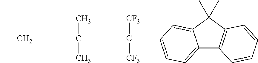
- a straight-chain, branched, or cyclic alkyl group such as a methyl group, an ethyl group, a propyl group, an isopropyl group, an n-butyl group, a tert-butyl group, or a cyclohexyl group, a straight-chain, branched, or cyclic alkenyl group such as a vinyl group, an allyl group, a propenyl group, a butenyl group, a hexenyl group, or a cyclohexenyl group, an aryl group such as a phenyl group or a tolyl group, an aralkyl group such as a benzyl group or a phenylethyl group, and others.
- n represents an integer number from 1 to 100.
- m represents an integer number of 1 to 80.
- a preferably meets more preferably meets 0.2 ⁇ a ⁇ 0.8, or especially preferably meets 0.3 ⁇ a ⁇ 0.7
- b preferably meets 0 ⁇ b ⁇ 1.0, more preferably meets 0.2 ⁇ b ⁇ 0.8, or especially preferably meets 0.2 ⁇ b ⁇ 0.5
- c preferably meets 0 ⁇ c ⁇ 0.3 or especially preferably meets and d preferably meets 0 ⁇ d ⁇ 0.3 or preferably meets 0 ⁇ d ⁇ 0.2.
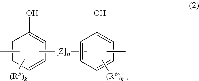
- each of X and Y represents a bivalent organic group represented by the general formula (2) or the general formula (3).
- the bivalent organic group represented by the general formula (2) or the general formula (3) is a bivalent aromatic group having a phenolic hydroxyl group or a glycidoxy group.
- n 0 or 1.
- R 5 and R 6 represent an alkyl group or an alkoxy group having carbon numbers of 1 to 4, which may be the same or different.
- R 5 and R 6 there are a methyl group, an ethyl group, an isopropyl group, a tert-butyl group, a methoxy group, an ethoxy group, an isopropyloxy group, and others.
- k represents one of 0, 1, and 2.
- R 7 and R 8 represent an alkyl group or an alkoxy group having carbon numbers of 1 to 4, which may be the same or different. As specific examples of R 7 and R 8 , there are groups equal to R 5 and R 6 . Further, h represents one of 0, 1, and 2.
- a weight average molecular weight of the silicone-backbone-containing polymer represented by the general formula (1) is 3,000 to 500,000.
- the range of 5,000 to 300,000 is preferable.
- the weight average molecular weight is a polystyrene equivalent based on gel permeation chromatography (GPC) in the present invention.
- the silicone-backbone-containing polymer represented by the general formula (1) can be manufactured in the presence of a catalyst by effecting a so-called “hydro-silylation” polymerizing reaction with respect to hydrogen silphenylene (1,4-bis(dimethylsilyl)benzene) of the following formula (4),
- the weight average molecular weight of the silicone-backbone-containing polymer represented by the general formula (1) can be readily controlled by adjusting a ratio of a total number of allyl groups of a specific epoxy group-containing compound having a diallyl group represented by the formula (6) and a specific phenol compound having a diallyl group represented by the formula (7) to a total number of hydrosilyl groups of hydrogensilphenylene represented by the formula (4) and dihydroorganosiloxane represented by the formula (5) (the total number of allyl groups/the total number of hydrosilyl groups).
- the specific epoxy group-containing compound having a diallyl group the formula (6)
- the specific phenol compound having a diallyl group the formula (7)
- hydrogensilphenylen the formula (4)
- dihydroorganosiloxane the formula (5)
- using a monoallyl compound such as o-allylphenol, or monohydrosilane such as triethylhydrosilane or monohydrosiloxane as a molecular weight modifier enables readily controlling the weight average molecular weight.
- platinum group metal simple substance such as platinum (including platinum black), rhodium, or palladium
- platinum chloride a chloroplatinic acid, and chloroplatinate
- a material obtained by supporting a platinum group metal such as platinum black or palladium by a carrier such as alumina, silica, or carbon a rhodium-olefin complex; chlorotris (triphenylphosphine) rhodium (a so-called Wilkinson's catalyst); a complex of platinum chloride, a chloroplatinic acid, or chloroplatinate and vinyl group-containing siloxane (vinyl group-containing cyclic siloxane in particular); and others.
- Its amount used is a catalytic amount, and 0.001 to 0.1 mass % is usually preferable with respect to a total amount of a reactive material to be polymerized as the platinum group metal.
- a solvent may be used as required.
- a hydrocarbon solvent such as toluene or xylene is preferable.
- a polymerization temperature range of, e.g., 40 to 150° C. or especially 60 to 120° C. is preferable.
- the solvent is evaporated if the solvent is used, whereby the silicone-backbone-containing polymer represented by the general formula (1) can be obtained.
- the cross-linking agent according to the present invention is contained in the first film layer and the second film layer.
- an epoxy compound is preferable as the cross-linking agent.
- the cross-linking agent according to the present invention can be solely contained, or two types or more of the same may be contained.
- the epoxy compound as the cross-linking agent there are a phenol novolac-type epoxy resin, a cresol novolac-type epoxy resin, a bisphenol A type epoxy resin such as diglycidyl bisphenol A, a bisphenol F type epoxy resin such as diglycidyl bisphenol F, a triphenylmethane type epoxy resin such as triphenylolpropanetriglycidylether, a cyclic aliphatic epoxy resin such as 3,4-epoxycyclohexylmethyl-3,4-epoxycyclohexanecarboxylate, a glycidyl ester resin such as diglycidyl phthalate, diglycidyl hexahydrophthalate, or dimethyl glycidyl phthalate, a glycidyl amine resin such as tetraglycidyl diaminodiphenylmethane, triglycidyl-p-aminophenol, diglycid
- a monofunctional epoxy compound containing one epoxy group per molecule may be added as the cross-linking agent according to the present invention as required.
- the first film layer becomes further superior in low-warp properties and wafer protection properties, and the second film layer can have further excellent filling properties with respect to a wafer surface, which is preferable.
- an additive amount of the cross-linking agent is preferably 3 to 80 mass % or more preferably 5 to 50 mass %.
- the filler according to the present invention is contained in the first film layer and, when a content rate of the filler contained in the first film layer is 100, the filler is contained in the second film layer in such a manner that a content rate becomes 0 or above and less than 100.
- the filler is not restricted in particular, there are a silica fine powder, composite silicone rubber fine particles, silicone fine particles, acrylic fine particles, and others as examples of preferable use, and one type alone selected from known materials may be used, or two or more types selected from the same may be combined and used.
- the silica fine powder for example, there are reinforcing silica such as fumed silica or precipitated silica; and crystalline silica such as quartz.
- the silica fine powder is exemplified by Aerosil R972, R974, and R976 manufactured by Nippon Aerosil Co., Ltd.; SE-2050, SC-2050, SE-1050, SO-E1, SO-C1, SO-E2, SO-C2, SO-E3, SO-C3, SO-E5, and SO-C5 manufactured by Admatechs Co., Ltd.; and Musil120A and Musil130A manufactured by Shin-Etsu Chemical Co., Ltd.
- composite silicone rubber fine particles for example, KMP-600, KMP-605, X-52-7030 manufactured by Shin-Etsu Chemical Co., Ltd. and others can be used.
- silicone fine particles for example, KMP-594, KMP-597, KMP-590, and X-52-821 manufactured by Shin-Etsu Chemical Co., Ltd. and others can be used.
- acrylic fine particles for example, art pearl G-400, G-800, GR-400 manufactured by Negami Chemical Industrial Co., Ltd. and others can be used.
- a content of the filler contained in the first film layer according to the present invention is not restricted in particular, when a total mass of the first film layer is assumed to be 100 mass %, the content of the filler is preferably 60 to 98 mass % or more preferably 75 to 93 mass %. Furthermore, when a content rate of the filler contained in the first film layer is assumed to be 100, as long as the content rate becomes 0 or above and less than 100, a content of the filler contained in the second film layer is preferably 0 to 90 mass % or more preferably 5 to 50 mass %. The further excellent low-warp properties and wafer protection properties can be obtained when the content of the filler contained in the first film layer is 60 mass or above, and excellent moldability can be obtained when this content is 98 mass % or below.
- various kinds of hardening accelerators may be used for the purpose of accelerating a reaction of the epoxy compound which is the cross-linking agent.
- the hardening accelerator there are an organic phosphine compound such as triphenylphosphine or tricyclohexylphosphine, an amino compound such as trimethylhexamethylenediamine, diaminodiphenylmethane, 2-(dimethylaminomethyl)phenol, 2,4,6-tris(dimethylaminomethyl)phenol, or triethanolamino, and an imidazole compound such as 2-methylimidazole, 2-ethylimidazole, 2-phenylimidazole, or 2-phenyl-4,5-dihydroxymethylimidazole.
- carbon functional silane may be added for the purpose of improving adhesion properties with respect to a wafer.
- the film-like wafer mold material according to the present invention can have a support film.
- the support film may be a single film or a multilayer film obtained by laminating a plurality of polymer films.
- a material there is a synthetic resin film made of polyethylene, polypropylene, polycarbonate, or polyethylene terephthalate, but polyethylene terephthalate having appropriate flexibility, mechanical strength, and heat resistance is preferable.
- these types of support films may be subjected to various kinds of processing such as a corona treatment or application of a delaminating agent.
- the wafer mold material formed into a film-like shape according to the present invention can have a protective film.
- the protective film the same film as the support film can be used, but polyethylene terephthalate and polyethylene having appropriate flexibility are preferable.
- polyethylene terephthalate can be exemplified by products already described above, and polyethylene can be exemplified by GF-8 (manufactured by Tamapoly Co., Ltd.) and PE film 0 type (manufactured by Nippa Co., Ltd.).
- a thickness of each of the support film and the protective film is preferably 10 to 100 ⁇ m or more specifically 25 to 50 ⁇ m.
- a wafer to be molded using the wafer mold material according to the present invention in a lump is not restricted in particular, but it is possible to adopt either a wafer having a semiconductor element (a chip) mounted on a surface thereof or a semiconductor wafer having a semiconductor element fabricated on a surface thereof.
- the film-like wafer mold material according to the present invention has excellent filling properties with respect to such a wafer surface before molding, and it also has low-warp properties and excellent protection properties for such a wafer after molding.
- the wafer mold material according to the present invention is not restricted in particular, it can be preferably used for molding a wafer having a large diameter, e.g., 8 inches (200 mm) or 12 inches (300 mm) or a thin-film wafer.
- a method for Manufacturing the film-like wafer mold material according to the present invention is not restricted in particular, there are, e.g., a method for fabricating the first film layer and the second film layer and attaching these layers to each other to realize a multilayer type, a method for fabricating one of the first film layer and the second film layer and fabricating the other film layer on this film layer, and others. These manufacturing methods can be appropriately determined in view of characteristics of the first and second films, solubility, and others.
- the thus-obtained film-like wafer mold material enables molding a wafer in a lump (wafer molding) and has excellent transference performance with respect to a thin-film wafer having a large diameter in particular and low-warp properties and excellent wafer protection performance after molding, and it can serve as the film-like wafer mold material that can be preferably used for a wafer level package.
- a hardened film of the film-like wafer mold material after molding is superior in flexibility, adhesion properties, heat resistance, and electrical characteristics and has low-stress properties and wafer protection performance required for the wafer mold material, and hence this material can be preferably used as a protective mold material for a very thin wafer.
- the method for molding a wafer using the film-like wafer mold material according to the present invention is not restricted in particular, the method can be realized by, e.g., delaminating a protective film attached to the upper side of the second film layer, using a vacuum laminator manufactured by Takatori Corporation (a product name: TEAM-100RF), setting a degree of vacuum in the vacuum chamber to 100 Pa, closely attaching the second film layer side of the film layer on the support film to the wafer at 100° C., restoring a pressure to a normal pressure, then cooling the substrate to 25° C. to be taken out from the vacuum laminator, and delaminating the support film.
- a vacuum laminator manufactured by Takatori Corporation (a product name: TEAM-100RF)
- the present invention provides a wafer molded in a lump with the film-like wafer mold material.
- the molded wafer that has less warp and is sufficiently protected can be obtained.
- the wafer protection properties can be excellently realized, and the wafer is protected in a better state, which is preferable.
- the present invention provides a semiconductor device obtained by dividing the molded wafer into individual pieces.
- the semiconductor device obtained by dividing the wafer that is less warped and sufficiently protected into individual pieces as described above becomes a high-quality semiconductor device having a good yield rate.
- Synthesis examples of the silicone-backbone-containing polymer according to the present invention Synthesis examples of the silicone-backbone-containing polymer according to the present invention, composition examples of a composition before forming the film layers according to the present invention, and examples and comparative examples of the film-like wafer mold material according to the present invention will be given below to explain the present invention in more detail, but the present invention is not restricted thereto.
- Chemical structure formulas of compounds (M-1) to (M-6) used in Synthesis Examples 1 and 2 of the silicone-backbone-containing polymer according to the present invention are as follows.
- the solvent in this silicone-backbone-containing polymer solution was evaporated under a reduced pressure, and 2,000 g of cyclopentanone was added to obtain the silicone-backbone-containing polymer solution containing cyclopentanone having a solid content concentration of 60 mass % as a main solvent.
- a molecular weight of the silicone-backbone-containing polymer in this silicone-backbone-containing polymer solution was measured based on GPC, a weight average molecular weight was 42,000 as a polystyrene equivalent, and a was 0, b was 1, c was 0, and d was 0 in the general formula (1).
- the solvent in this silicone-backbone-containing polymer solution was evaporated under a reduced pressure, and 980 g of cyclopentanone was added to obtain the silicone-backbone-containing polymer solution containing cyclopentanone having a solid content concentration of 60 mass % as a main solvent.
- a molecular weight of the silicone-backbone-containing polymer in this silicone-backbone-containing polymer solution was measured based on the GPC, a weight average molecular weight was 64,000 as a polystyrene equivalent, and a was 0.480, b was 0.320, c was 0.120, and d was 0.080 in the general formula (1).
- RE-310S (a bisphenol A type epoxy resin, manufactured by Japan Epoxy Resin Co., Ltd.)
- Epicoat 630 (a polyfunctional epoxy resin, manufactured by Japan Epoxy Resin Co., Ltd.)
- Example 1 Example 2
- Example 3 Example 4 Silicone- Synthesis Synthesis Synthesis Synthesis backbone-
- Example 1 Example 2
- Example 2 containing (9 pars by (70.9 parts (11.9 parts (59.5 parts polymer mass) by mass) by mass) Cross-linking RE-310S RE-310S Epicoat 630
- Epicoat 630 agent (1 part by (9 parts by (2.1 parts (10.5 parts mass) mass) by mass) by mass)
- Filler SE-2050 SE-2050 SE-2050 SE-2050 (90 parts (20 parts (86 parts (30 parts by mass) by mass) by mass) by mass) by mass) by mass) by mass)
- Cross-linking 2PHZ 2PHZ — — accelerator 0.1 part (0.1 part by mass) by mass
- a die coater as a film coater and a polyethylene terephthalate film (a thickness: 38 ⁇ m) were used, and each of the compositions before forming the film layers according to Composition.
- Examples 1 to 4 was applied to the upper side of the polyethylene terephthalate film. Then, this material was passed through a circulating hot air oven (a length: 4 m) set to 100° C. for five minutes to form a film layer having a film thickness of 50 ⁇ m to 400 ⁇ m on the polyethylene terephthalate film. Then, a polyethylene film (a thickness: 50 ⁇ m) was attached to the upper side of the film layer under a pressure of 1 MPa using a laminated roll, thereby fabricating each film layer.
- a silicon wafer having a wafer thickness of 100 ⁇ m and a diameter of 8 inches (200 mm) was prepared.
- a polyethylene terephthalate film (a protective film) on the second film layer side was delaminated, a vacuum laminator manufactured by Takatori Corporation (a product name: TEAM-100RF) was used, the inside of the vacuum chamber was set to a degree of vacuum 100 Pa, and the second film layer side was closely attached to the silicon wafer at 100° C. After restoring a pressure to a normal pressure, the silicon wafer was cooled to 25° C. and taken out from the vacuum laminator, and the polyethylene terephthalate film (a support film) on the first film layer side was delaminated.
- the following table shows transference performance with respect to a wafer, wafer protection performance, and an amount of warp. It is to be noted that the transference performance with respect to a wafer were determined to be good if transference to the wafer was successful after delamination from the support film. Furthermore, in regard to the wafer protection performance, an amount of deflection of the wafer was measured when supporting an end of the wafer, a value equal to or below 20 mm was determined to be good, and a value exceeding 20 mm was determined as a failure.
- the amount of warp is a value obtained by measuring warp of the wafer at a wafer end with reference to a wafer center.
- Example 3 Example 1 Example 2 First film Composition Composition Composition Composition Composition None layer Example 1 Example 3 Example 1 Example 1 (Thickness: (Thickness: (Thickness: (Thickness: 100 ⁇ m) 100 ⁇ m) 50 ⁇ m) 100 ⁇ m) Second film Composition Composition Composition None Composition layer Example 2 Example 4 Example 2 Example 4 (Thickness: (Thickness: (Thickness: (Thickness: 400 ⁇ m) 300 ⁇ m) 100 ⁇ m) 300 ⁇ m) transference Good Good Good Good Good Non- Good performance transferable Wafer Good Good Good Good Good — Poor protection properties Amount of ⁇ 1 ⁇ 1 ⁇ 1 — ⁇ 1 warp (mm)
- Comparative Example 1 using the first film layer alone has poor transference performance
- Comparative Example 2 using the second film layer alone has poor wafer protection performance.
- Examples 1 to 3 according to the present invention having the multilayer structure including the first and second film layers can provide the film-like wafer mold material having excellent transference performance and wafer protection performance and a small amount of warp.
- the film-like wafer mold material according to the present invention since the film-like wafer mold material according to the present invention has the film-like shape, it enables molding a wafer (wafer molding) in a lump, has the excellent transference performance with respect to a large-diameter thin-film wafer, and also has excellent filling properties with respect to a wafer surface before molding and low-warp properties and excellent wafer protection performance after molding at the same time because it has the multilayer structure including two types of films different from each other in performance, i.e., the high-filler type first film layer superior in low-warp properties and wafer protection properties and the low-filler type second film layer that has the excellent filling properties with respect to the wafer surface and enables molding the wafer in a lump, thereby providing the film-like wafer mold material that can be preferably used for a wafer level package.
Landscapes
- Chemical & Material Sciences (AREA)
- Organic Chemistry (AREA)
- Chemical Kinetics & Catalysis (AREA)
- Polymers & Plastics (AREA)
- Health & Medical Sciences (AREA)
- Medicinal Chemistry (AREA)
- Materials Engineering (AREA)
- Wood Science & Technology (AREA)
- Engineering & Computer Science (AREA)
- Life Sciences & Earth Sciences (AREA)
- Laminated Bodies (AREA)
- Structures Or Materials For Encapsulating Or Coating Semiconductor Devices Or Solid State Devices (AREA)
- Compositions Of Macromolecular Compounds (AREA)
Abstract
Description

wherein R1 to R4 may be the same or different and represent univalent hydrocarbon groups having carbon numbers from 1 to 8; m represents an integer number from 1 to 100; each of a, b, c, and d represents 0 or a positive number, and satisfies a+b+c+d=1; further, each of X and Y represents a bivalent organic group represented by the following general formula (2) or the following general formula (3),

wherein Z represents a bivalent organic group selected from the following chemical structures;
and n represents 0 or 1; each of R5 or R6 represents an alkyl group or an alkoxy group having a carbon number from 1 to 4, and may be the same or different; k represents any one of 0, 1, and 2,

wherein V represents a bivalent organic group selected from the following chemical structures;

and p represents 0 or 1; each of R7 and R8 represents an alkyl group or an alkoxy group having a carbon number from 1 to 4, and may be the same or different; h represents any one of 0, 1, and 2.
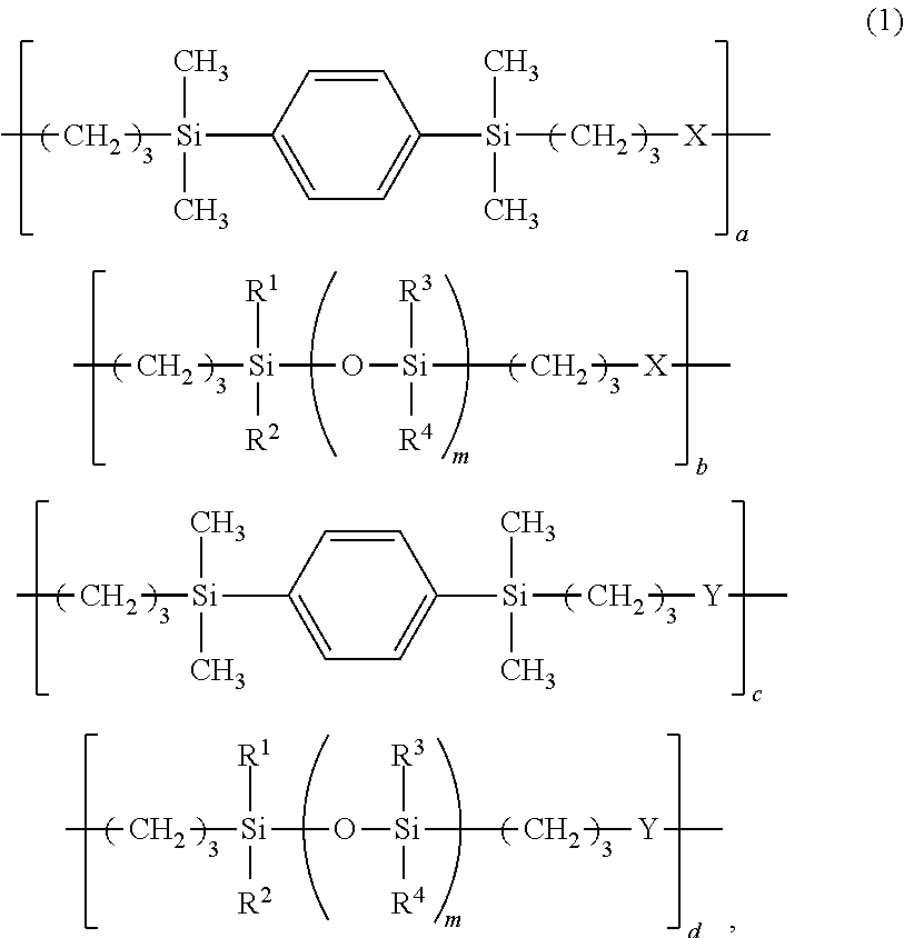
wherein R1 to R4 may be the same or different and represent univalent hydrocarbon groups having carbon numbers from 1 to 8; m represents an integer number from 1 to 100; each of a, b, c, and d represents 0 or a positive number, and satisfies a+b+c+d=1; further, each of X and Y represents a bivalent organic group represented by the following general formula (2) or the following general formula (3),
wherein Z represents a bivalent organic group selected from the following chemical structures;

and n represents 0 or 1; each of R5 or R6 represents an alkyl group or an alkoxy group having a carbon number from 1 to 4, and may be the same or different; k represents any one of 0, 1, and 2,

wherein V represents a bivalent organic group selected from the following chemical structures;

and p represents 0 or 1; each of R7 and R8 represents an alkyl group or an alkoxy group having a carbon number from 1 to 4, and may be the same or different; h represents any one of 0, 1, and 2.

or this hydrogen silphenylene, dihydroorganosiloxane of the following general formula (5),

wherein R3, R4, and m represent equal to those described above, a specific epoxy group-containing compound having a diallyl group represented by the following general formula (6),

wherein V, R7, R8, p, and h represent equal to those described above, and a specific phenol compound having a diallyl group represented by the following general formula (7),

wherein Z, R5, R6, n, and k represent equal to those described above.

| TABLE 1 | ||
| Composition | ||
| Composition | Composition | Composition | Composition | ||
| Example 1 | Example 2 | Example 3 | Example 4 | ||
| Silicone- | Synthesis | Synthesis | Synthesis | Synthesis |
| backbone- | Example 1 | Example 1 | Example 2 | Example 2 |
| containing | (9 pars by | (70.9 parts | (11.9 parts | (59.5 parts |
| polymer | mass) | by mass) | by mass) | by mass) |
| Cross-linking | RE-310S | RE-310S | Epicoat 630 | Epicoat 630 |
| agent | (1 part by | (9 parts by | (2.1 parts | (10.5 parts |
| mass) | mass) | by mass) | by mass) | |
| Filler | SE-2050 | SE-2050 | SE-2050 | SE-2050 |
| (90 parts | (20 parts | (86 parts | (30 parts | |
| by mass) | by mass) | by mass) | by mass) | |
| Cross-linking | 2PHZ | 2PHZ | — | — |
| accelerator | (0.1 part | (0.1 part | ||
| by mass) | by mass) | |||
[Formation of Film Layers]
| TABLE 2 | ||||||
| Comparative | Comparative | |||||
| Example 1 | Example 2 | Example 3 | Example 1 | Example 2 | ||
| First film | Composition | Composition | Composition | Composition | None |
| layer | Example 1 | Example 3 | Example 1 | Example 1 | |
| (Thickness: | (Thickness: | (Thickness: | (Thickness: | ||
| 100 μm) | 100 μm) | 50 μm) | 100 μm) | ||
| Second film | Composition | Composition | Composition | None | Composition |
| layer | Example 2 | Example 4 | Example 2 | Example 4 | |
| (Thickness: | (Thickness: | (Thickness: | (Thickness: | ||
| 400 μm) | 300 μm) | 100 μm) | 300 μm) | ||
| transference | Good | Good | Good | Non- | Good |
| performance | transferable | ||||
| Wafer | Good | Good | Good | — | Poor |
| protection | |||||
| properties | |||||
| Amount of | <1 | <1 | <1 | — | <1 |
| warp (mm) | |||||
Claims (9)


Applications Claiming Priority (2)
| Application Number | Priority Date | Filing Date | Title |
|---|---|---|---|
| JP2011-058464 | 2011-03-16 | ||
| JP2011058464A JP5512580B2 (en) | 2011-03-16 | 2011-03-16 | Film mold material, molded semiconductor wafer, and semiconductor device |
Publications (2)
| Publication Number | Publication Date |
|---|---|
| US20120235284A1 US20120235284A1 (en) | 2012-09-20 |
| US9929068B2 true US9929068B2 (en) | 2018-03-27 |
Family
ID=45855456
Family Applications (1)
| Application Number | Title | Priority Date | Filing Date |
|---|---|---|---|
| US13/410,887 Active 2035-11-16 US9929068B2 (en) | 2011-03-16 | 2012-03-02 | Film-like wafer mold material, molded wafer, and semiconductor device |
Country Status (5)
| Country | Link |
|---|---|
| US (1) | US9929068B2 (en) |
| EP (1) | EP2500934B1 (en) |
| JP (1) | JP5512580B2 (en) |
| KR (1) | KR101588488B1 (en) |
| TW (1) | TWI630641B (en) |
Families Citing this family (11)
| Publication number | Priority date | Publication date | Assignee | Title |
|---|---|---|---|---|
| JP5459196B2 (en) * | 2009-12-15 | 2014-04-02 | 信越化学工業株式会社 | Photocurable dry film, method for producing the same, pattern forming method, and film for protecting electric / electronic parts |
| JP5623970B2 (en) * | 2011-04-22 | 2014-11-12 | 信越化学工業株式会社 | Resin laminate, semiconductor device and manufacturing method thereof |
| JP5981384B2 (en) * | 2013-04-16 | 2016-08-31 | 信越化学工業株式会社 | Resin composition, resin film, semiconductor device and manufacturing method thereof |
| JP6098531B2 (en) * | 2014-01-23 | 2017-03-22 | 信越化学工業株式会社 | Resin composition, resin film, semiconductor device and manufacturing method thereof |
| JP6265105B2 (en) | 2014-10-30 | 2018-01-24 | 信越化学工業株式会社 | Silicone resin, resin composition, resin film, semiconductor device and manufacturing method thereof |
| JP6361566B2 (en) * | 2015-04-24 | 2018-07-25 | 信越化学工業株式会社 | Resin composition, resin film, semiconductor device and manufacturing method thereof |
| JP6866802B2 (en) | 2017-08-09 | 2021-04-28 | 信越化学工業株式会社 | Silicone skeleton-containing polymer compound, photosensitive resin composition, photosensitive resin film, photosensitive dry film, laminate, and pattern forming method |
| JP6874584B2 (en) | 2017-08-09 | 2021-05-19 | 信越化学工業株式会社 | Photosensitive resin composition, photosensitive resin film, photosensitive dry film, laminate, and pattern forming method |
| JP6870657B2 (en) * | 2018-05-17 | 2021-05-12 | 信越化学工業株式会社 | Photosensitive resin composition, photosensitive dry film, and pattern forming method |
| US11548985B2 (en) | 2018-11-28 | 2023-01-10 | Shin-Etsu Chemical Co., Ltd. | Siloxane polymer containing isocyanuric acid and polyether skeletons, photosensitive resin composition, pattern forming process, and fabrication of opto-semiconductor device |
| JP7056541B2 (en) | 2018-12-19 | 2022-04-19 | 信越化学工業株式会社 | Photosensitive resin composition, photosensitive dry film and pattern forming method |
Citations (15)
| Publication number | Priority date | Publication date | Assignee | Title |
|---|---|---|---|---|
| US3159601A (en) | 1962-07-02 | 1964-12-01 | Gen Electric | Platinum-olefin complex catalyzed addition of hydrogen- and alkenyl-substituted siloxanes |
| US3159662A (en) | 1962-07-02 | 1964-12-01 | Gen Electric | Addition reaction |
| US3220972A (en) | 1962-07-02 | 1965-11-30 | Gen Electric | Organosilicon process using a chloroplatinic acid reaction product as the catalyst |
| US3775452A (en) | 1971-04-28 | 1973-11-27 | Gen Electric | Platinum complexes of unsaturated siloxanes and platinum containing organopolysiloxanes |
| JPS6151858A (en) | 1984-08-20 | 1986-03-14 | Mitsubishi Electric Corp | Resin seal type semiconductor device |
| US20020055550A1 (en) * | 2000-09-12 | 2002-05-09 | Shin-Etsu Chemical Co. Ltd. | Organosiloxane polymer, photo-curable resin composition, patterning process, and substrate protective coating |
| US20020089067A1 (en) | 2000-11-14 | 2002-07-11 | Loctite Corporation | Wafer applied fluxing and underfill material, and layered electronic assemblies manufactured therewith |
| JP2003048989A (en) * | 2001-08-09 | 2003-02-21 | Nippon Unicar Co Ltd | Dialkenyldiepoxybisphenol-polysiloxane alternate copolymer or derivative of the same and epoxy resin composition for electronic material obtained by blending the same |
| JP2003268203A (en) * | 2002-03-18 | 2003-09-25 | Shin Etsu Chem Co Ltd | Liquid epoxy resin composition for wafer mold and semiconductor device using the same |
| US6747115B2 (en) | 2000-05-31 | 2004-06-08 | Shin-Etsu Chemical Co., Ltd. | Silicone polymer, silicone composition, and cosmetic preparation containing the same |
| DE102006009696A1 (en) | 2006-03-02 | 2007-09-06 | Forschungszentrum Jülich GmbH | Component for nano- and molecular electronics |
| US20080182087A1 (en) * | 2007-01-31 | 2008-07-31 | Shin-Etsu Chemical Co., Ltd. | Silphenylene-bearing polymer, photo-curable resin composition, patterning process, and substrate circuit protective film |
| JP2009141020A (en) | 2007-12-04 | 2009-06-25 | Furukawa Electric Co Ltd:The | Electronic component sealing sheet |
| WO2009142065A1 (en) | 2008-05-21 | 2009-11-26 | ナガセケムテックス株式会社 | Epoxy resin composition for encapsulating electronic part |
| US20110143092A1 (en) * | 2009-12-15 | 2011-06-16 | Satoshi Asai | Photocurable dry film, method for preparing same, patterning method and film for protecting electric and electronic parts |
-
2011
- 2011-03-16 JP JP2011058464A patent/JP5512580B2/en active Active
-
2012
- 2012-03-02 US US13/410,887 patent/US9929068B2/en active Active
- 2012-03-05 EP EP12001467.5A patent/EP2500934B1/en active Active
- 2012-03-15 TW TW101108843A patent/TWI630641B/en active
- 2012-03-15 KR KR1020120026392A patent/KR101588488B1/en active Active
Patent Citations (19)
| Publication number | Priority date | Publication date | Assignee | Title |
|---|---|---|---|---|
| US3159662A (en) | 1962-07-02 | 1964-12-01 | Gen Electric | Addition reaction |
| US3220972A (en) | 1962-07-02 | 1965-11-30 | Gen Electric | Organosilicon process using a chloroplatinic acid reaction product as the catalyst |
| US3159601A (en) | 1962-07-02 | 1964-12-01 | Gen Electric | Platinum-olefin complex catalyzed addition of hydrogen- and alkenyl-substituted siloxanes |
| US3775452A (en) | 1971-04-28 | 1973-11-27 | Gen Electric | Platinum complexes of unsaturated siloxanes and platinum containing organopolysiloxanes |
| JPS6151858A (en) | 1984-08-20 | 1986-03-14 | Mitsubishi Electric Corp | Resin seal type semiconductor device |
| US6747115B2 (en) | 2000-05-31 | 2004-06-08 | Shin-Etsu Chemical Co., Ltd. | Silicone polymer, silicone composition, and cosmetic preparation containing the same |
| US20020055550A1 (en) * | 2000-09-12 | 2002-05-09 | Shin-Etsu Chemical Co. Ltd. | Organosiloxane polymer, photo-curable resin composition, patterning process, and substrate protective coating |
| US20020089067A1 (en) | 2000-11-14 | 2002-07-11 | Loctite Corporation | Wafer applied fluxing and underfill material, and layered electronic assemblies manufactured therewith |
| JP2003048989A (en) * | 2001-08-09 | 2003-02-21 | Nippon Unicar Co Ltd | Dialkenyldiepoxybisphenol-polysiloxane alternate copolymer or derivative of the same and epoxy resin composition for electronic material obtained by blending the same |
| JP2003268203A (en) * | 2002-03-18 | 2003-09-25 | Shin Etsu Chem Co Ltd | Liquid epoxy resin composition for wafer mold and semiconductor device using the same |
| DE102006009696A1 (en) | 2006-03-02 | 2007-09-06 | Forschungszentrum Jülich GmbH | Component for nano- and molecular electronics |
| US20080182087A1 (en) * | 2007-01-31 | 2008-07-31 | Shin-Etsu Chemical Co., Ltd. | Silphenylene-bearing polymer, photo-curable resin composition, patterning process, and substrate circuit protective film |
| EP1953183A2 (en) | 2007-01-31 | 2008-08-06 | Shin-Etsu Chemical Co., Ltd. | Silphenylene-bearing polymer, photo-curable resin composition, patterning process, and substrate circuit protective film |
| JP2009141020A (en) | 2007-12-04 | 2009-06-25 | Furukawa Electric Co Ltd:The | Electronic component sealing sheet |
| WO2009142065A1 (en) | 2008-05-21 | 2009-11-26 | ナガセケムテックス株式会社 | Epoxy resin composition for encapsulating electronic part |
| EP2280044A1 (en) | 2008-05-21 | 2011-02-02 | Nagase ChemteX Corporation | Epoxy resin composition for encapsulating electronic part |
| US20110105646A1 (en) | 2008-05-21 | 2011-05-05 | Nagase Chemtex Corporation | Epoxy resin composition for encapsulating electronic part |
| US20110143092A1 (en) * | 2009-12-15 | 2011-06-16 | Satoshi Asai | Photocurable dry film, method for preparing same, patterning method and film for protecting electric and electronic parts |
| TW201137523A (en) | 2009-12-15 | 2011-11-01 | Shinetsu Chemical Co | Photocurable dry film, method for preparing same, patterning method and film for protecting electric and electronic parts |
Non-Patent Citations (10)
| Title |
|---|
| Aug. 13, 2015 Office Action issued in Taiwanese Application No. 101108843. |
| English language machine translation JPO JP 2003048989 (2003). * |
| English machine translation of JP 2003268203. * |
| European Office Action issued in Application No. 12 001 467.5; dated Nov. 15, 2013. |
| Japanese Office Action issued in Application No. 2011-058464; dated Jul. 25, 2013 (With Partial English-language translation). |
| Jun. 17, 2015 Office Action issued in Korean Application No. 2012-0026392. |
| Mar. 16, 2015 Official Communication issued in European Application No. 12 001 467.5. |
| May 5, 2017 Office Action in Taiwanese Application No. 101108843. |
| Oct. 24, 2016 Office Action issued in Taiwanese Patent Application No. 101108843. |
| Sep. 25, 2012 Extended European Search Report issued in European Patent Application No. 12001467.5. |
Also Published As
| Publication number | Publication date |
|---|---|
| TWI630641B (en) | 2018-07-21 |
| KR20120106609A (en) | 2012-09-26 |
| EP2500934A3 (en) | 2012-10-24 |
| KR101588488B1 (en) | 2016-01-25 |
| EP2500934A2 (en) | 2012-09-19 |
| EP2500934B1 (en) | 2015-10-21 |
| JP2012195458A (en) | 2012-10-11 |
| TW201303965A (en) | 2013-01-16 |
| US20120235284A1 (en) | 2012-09-20 |
| JP5512580B2 (en) | 2014-06-04 |
Similar Documents
| Publication | Publication Date | Title |
|---|---|---|
| US9929068B2 (en) | Film-like wafer mold material, molded wafer, and semiconductor device | |
| JP5623970B2 (en) | Resin laminate, semiconductor device and manufacturing method thereof | |
| CN105960426B (en) | Resin composition, resin film, semiconductor device, and manufacturing method thereof | |
| CN105566913B (en) | Silicone resin, resin composition, resin film, semiconductor device, and manufacturing method | |
| TWI683862B (en) | Resin composition, resin film, semiconductor device and manufacturing method thereof | |
| US10730273B2 (en) | Resin composition, resin film, semiconductor laminate, method for manufacturing semiconductor laminate, and method for manufacturing semiconductor device | |
| TW201236116A (en) | Wafer mold material and method for manufacturing semiconductor apparatus | |
| US8883913B2 (en) | Resin composition, resin film, semiconductor device, and production method thereof | |
| US10428239B2 (en) | Resin composition, resin film, method for producing resin film, method for producing semiconductor device, and semiconductor device | |
| US10850482B2 (en) | Resin composition, resin film, semiconductor laminate, method for manufacturing semiconductor laminate, and method for manufacturing semiconductor device | |
| TWI728087B (en) | Resin composition, resin film, resin film manufacturing method, semiconductor device manufacturing method, and semiconductor device | |
| US10308787B2 (en) | Resin composition, resin film, method for producing resin film, method for producing semiconductor device, and semiconductor device | |
| JP5981384B2 (en) | Resin composition, resin film, semiconductor device and manufacturing method thereof | |
| JP2018030944A (en) | Resin composition, resin film, method for manufacturing semiconductor device, and semiconductor device |
Legal Events
| Date | Code | Title | Description |
|---|---|---|---|
| AS | Assignment |
Owner name: SHIN-ETSU CHEMICAL CO., LTD., JAPAN Free format text: ASSIGNMENT OF ASSIGNORS INTEREST;ASSIGNORS:SUGO, MICHIHIRO;KONDO, KAZUNORI;SIGNING DATES FROM 20120110 TO 20120210;REEL/FRAME:027808/0953 |
|
| STCF | Information on status: patent grant |
Free format text: PATENTED CASE |
|
| MAFP | Maintenance fee payment |
Free format text: PAYMENT OF MAINTENANCE FEE, 4TH YEAR, LARGE ENTITY (ORIGINAL EVENT CODE: M1551); ENTITY STATUS OF PATENT OWNER: LARGE ENTITY Year of fee payment: 4 |
|
| MAFP | Maintenance fee payment |
Free format text: PAYMENT OF MAINTENANCE FEE, 8TH YEAR, LARGE ENTITY (ORIGINAL EVENT CODE: M1552); ENTITY STATUS OF PATENT OWNER: LARGE ENTITY Year of fee payment: 8 |