US9911684B1 - Holes and dimples to control solder flow - Google Patents
Holes and dimples to control solder flow Download PDFInfo
- Publication number
- US9911684B1 US9911684B1 US15/240,423 US201615240423A US9911684B1 US 9911684 B1 US9911684 B1 US 9911684B1 US 201615240423 A US201615240423 A US 201615240423A US 9911684 B1 US9911684 B1 US 9911684B1
- Authority
- US
- United States
- Prior art keywords
- lead frame
- holes
- fluid
- dimples
- die
- Prior art date
- Legal status (The legal status is an assumption and is not a legal conclusion. Google has not performed a legal analysis and makes no representation as to the accuracy of the status listed.)
- Active, expires
Links
Images


Classifications
-
- H01L23/49541—
-
- H—ELECTRICITY
- H10—SEMICONDUCTOR DEVICES; ELECTRIC SOLID-STATE DEVICES NOT OTHERWISE PROVIDED FOR
- H10W—GENERIC PACKAGES, INTERCONNECTIONS, CONNECTORS OR OTHER CONSTRUCTIONAL DETAILS OF DEVICES COVERED BY CLASS H10
- H10W70/00—Package substrates; Interposers; Redistribution layers [RDL]
- H10W70/40—Leadframes
- H10W70/421—Shapes or dispositions
-
- H01L21/4828—
-
- H01L21/4842—
-
- H01L23/49503—
-
- H01L23/49513—
-
- H01L23/49575—
-
- H01L24/32—
-
- H01L24/40—
-
- H01L24/73—
-
- H01L24/84—
-
- H—ELECTRICITY
- H10—SEMICONDUCTOR DEVICES; ELECTRIC SOLID-STATE DEVICES NOT OTHERWISE PROVIDED FOR
- H10W—GENERIC PACKAGES, INTERCONNECTIONS, CONNECTORS OR OTHER CONSTRUCTIONAL DETAILS OF DEVICES COVERED BY CLASS H10
- H10W70/00—Package substrates; Interposers; Redistribution layers [RDL]
- H10W70/01—Manufacture or treatment
- H10W70/04—Manufacture or treatment of leadframes
- H10W70/042—Etching
-
- H—ELECTRICITY
- H10—SEMICONDUCTOR DEVICES; ELECTRIC SOLID-STATE DEVICES NOT OTHERWISE PROVIDED FOR
- H10W—GENERIC PACKAGES, INTERCONNECTIONS, CONNECTORS OR OTHER CONSTRUCTIONAL DETAILS OF DEVICES COVERED BY CLASS H10
- H10W70/00—Package substrates; Interposers; Redistribution layers [RDL]
- H10W70/01—Manufacture or treatment
- H10W70/04—Manufacture or treatment of leadframes
- H10W70/048—Mechanical treatments, e.g. punching, cutting, deforming or cold welding
-
- H—ELECTRICITY
- H10—SEMICONDUCTOR DEVICES; ELECTRIC SOLID-STATE DEVICES NOT OTHERWISE PROVIDED FOR
- H10W—GENERIC PACKAGES, INTERCONNECTIONS, CONNECTORS OR OTHER CONSTRUCTIONAL DETAILS OF DEVICES COVERED BY CLASS H10
- H10W70/00—Package substrates; Interposers; Redistribution layers [RDL]
- H10W70/40—Leadframes
- H10W70/411—Chip-supporting parts, e.g. die pads
- H10W70/417—Bonding materials between chips and die pads
-
- H—ELECTRICITY
- H10—SEMICONDUCTOR DEVICES; ELECTRIC SOLID-STATE DEVICES NOT OTHERWISE PROVIDED FOR
- H10W—GENERIC PACKAGES, INTERCONNECTIONS, CONNECTORS OR OTHER CONSTRUCTIONAL DETAILS OF DEVICES COVERED BY CLASS H10
- H10W70/00—Package substrates; Interposers; Redistribution layers [RDL]
- H10W70/40—Leadframes
- H10W70/421—Shapes or dispositions
- H10W70/424—Cross-sectional shapes
-
- H—ELECTRICITY
- H10—SEMICONDUCTOR DEVICES; ELECTRIC SOLID-STATE DEVICES NOT OTHERWISE PROVIDED FOR
- H10W—GENERIC PACKAGES, INTERCONNECTIONS, CONNECTORS OR OTHER CONSTRUCTIONAL DETAILS OF DEVICES COVERED BY CLASS H10
- H10W72/00—Interconnections or connectors in packages
- H10W72/60—Strap connectors, e.g. thick copper clips for grounding of power devices
-
- H—ELECTRICITY
- H10—SEMICONDUCTOR DEVICES; ELECTRIC SOLID-STATE DEVICES NOT OTHERWISE PROVIDED FOR
- H10W—GENERIC PACKAGES, INTERCONNECTIONS, CONNECTORS OR OTHER CONSTRUCTIONAL DETAILS OF DEVICES COVERED BY CLASS H10
- H10W90/00—Package configurations
- H10W90/811—Multiple chips on leadframes
-
- H01L2224/29191—
-
- H01L2224/32245—
-
- H01L2224/40245—
-
- H01L2224/73263—
-
- H01L2224/83192—
-
- H01L2224/83801—
-
- H01L2224/84801—
-
- H01L2224/92246—
-
- H01L2924/0665—
-
- H01L2924/07025—
-
- H01L2924/0715—
-
- H—ELECTRICITY
- H10—SEMICONDUCTOR DEVICES; ELECTRIC SOLID-STATE DEVICES NOT OTHERWISE PROVIDED FOR
- H10W—GENERIC PACKAGES, INTERCONNECTIONS, CONNECTORS OR OTHER CONSTRUCTIONAL DETAILS OF DEVICES COVERED BY CLASS H10
- H10W72/00—Interconnections or connectors in packages
- H10W72/071—Connecting or disconnecting
- H10W72/073—Connecting or disconnecting of die-attach connectors
- H10W72/07331—Connecting techniques
- H10W72/07336—Soldering or alloying
-
- H—ELECTRICITY
- H10—SEMICONDUCTOR DEVICES; ELECTRIC SOLID-STATE DEVICES NOT OTHERWISE PROVIDED FOR
- H10W—GENERIC PACKAGES, INTERCONNECTIONS, CONNECTORS OR OTHER CONSTRUCTIONAL DETAILS OF DEVICES COVERED BY CLASS H10
- H10W72/00—Interconnections or connectors in packages
- H10W72/071—Connecting or disconnecting
- H10W72/073—Connecting or disconnecting of die-attach connectors
- H10W72/07331—Connecting techniques
- H10W72/07337—Connecting techniques using a polymer adhesive, e.g. an adhesive based on silicone or epoxy
-
- H—ELECTRICITY
- H10—SEMICONDUCTOR DEVICES; ELECTRIC SOLID-STATE DEVICES NOT OTHERWISE PROVIDED FOR
- H10W—GENERIC PACKAGES, INTERCONNECTIONS, CONNECTORS OR OTHER CONSTRUCTIONAL DETAILS OF DEVICES COVERED BY CLASS H10
- H10W72/00—Interconnections or connectors in packages
- H10W72/071—Connecting or disconnecting
- H10W72/076—Connecting or disconnecting of strap connectors
- H10W72/07631—Techniques
- H10W72/07636—Soldering or alloying
-
- H—ELECTRICITY
- H10—SEMICONDUCTOR DEVICES; ELECTRIC SOLID-STATE DEVICES NOT OTHERWISE PROVIDED FOR
- H10W—GENERIC PACKAGES, INTERCONNECTIONS, CONNECTORS OR OTHER CONSTRUCTIONAL DETAILS OF DEVICES COVERED BY CLASS H10
- H10W72/00—Interconnections or connectors in packages
- H10W72/071—Connecting or disconnecting
- H10W72/076—Connecting or disconnecting of strap connectors
- H10W72/07651—Connecting or disconnecting of strap connectors characterised by changes in properties of the strap connectors during connecting
- H10W72/07653—Connecting or disconnecting of strap connectors characterised by changes in properties of the strap connectors during connecting changes in shapes
-
- H—ELECTRICITY
- H10—SEMICONDUCTOR DEVICES; ELECTRIC SOLID-STATE DEVICES NOT OTHERWISE PROVIDED FOR
- H10W—GENERIC PACKAGES, INTERCONNECTIONS, CONNECTORS OR OTHER CONSTRUCTIONAL DETAILS OF DEVICES COVERED BY CLASS H10
- H10W72/00—Interconnections or connectors in packages
- H10W72/30—Die-attach connectors
- H10W72/321—Structures or relative sizes of die-attach connectors
- H10W72/325—Die-attach connectors having a filler embedded in a matrix
-
- H—ELECTRICITY
- H10—SEMICONDUCTOR DEVICES; ELECTRIC SOLID-STATE DEVICES NOT OTHERWISE PROVIDED FOR
- H10W—GENERIC PACKAGES, INTERCONNECTIONS, CONNECTORS OR OTHER CONSTRUCTIONAL DETAILS OF DEVICES COVERED BY CLASS H10
- H10W72/00—Interconnections or connectors in packages
- H10W72/30—Die-attach connectors
- H10W72/351—Materials of die-attach connectors
- H10W72/352—Materials of die-attach connectors comprising metals or metalloids, e.g. solders
-
- H—ELECTRICITY
- H10—SEMICONDUCTOR DEVICES; ELECTRIC SOLID-STATE DEVICES NOT OTHERWISE PROVIDED FOR
- H10W—GENERIC PACKAGES, INTERCONNECTIONS, CONNECTORS OR OTHER CONSTRUCTIONAL DETAILS OF DEVICES COVERED BY CLASS H10
- H10W72/00—Interconnections or connectors in packages
- H10W72/30—Die-attach connectors
- H10W72/351—Materials of die-attach connectors
- H10W72/353—Materials of die-attach connectors not comprising solid metals or solid metalloids, e.g. ceramics
- H10W72/354—Materials of die-attach connectors not comprising solid metals or solid metalloids, e.g. ceramics comprising polymers
-
- H—ELECTRICITY
- H10—SEMICONDUCTOR DEVICES; ELECTRIC SOLID-STATE DEVICES NOT OTHERWISE PROVIDED FOR
- H10W—GENERIC PACKAGES, INTERCONNECTIONS, CONNECTORS OR OTHER CONSTRUCTIONAL DETAILS OF DEVICES COVERED BY CLASS H10
- H10W72/00—Interconnections or connectors in packages
- H10W72/30—Die-attach connectors
- H10W72/381—Auxiliary members
- H10W72/387—Flow barriers
-
- H—ELECTRICITY
- H10—SEMICONDUCTOR DEVICES; ELECTRIC SOLID-STATE DEVICES NOT OTHERWISE PROVIDED FOR
- H10W—GENERIC PACKAGES, INTERCONNECTIONS, CONNECTORS OR OTHER CONSTRUCTIONAL DETAILS OF DEVICES COVERED BY CLASS H10
- H10W72/00—Interconnections or connectors in packages
- H10W72/60—Strap connectors, e.g. thick copper clips for grounding of power devices
- H10W72/631—Shapes of strap connectors
-
- H—ELECTRICITY
- H10—SEMICONDUCTOR DEVICES; ELECTRIC SOLID-STATE DEVICES NOT OTHERWISE PROVIDED FOR
- H10W—GENERIC PACKAGES, INTERCONNECTIONS, CONNECTORS OR OTHER CONSTRUCTIONAL DETAILS OF DEVICES COVERED BY CLASS H10
- H10W72/00—Interconnections or connectors in packages
- H10W72/60—Strap connectors, e.g. thick copper clips for grounding of power devices
- H10W72/651—Materials of strap connectors
-
- H—ELECTRICITY
- H10—SEMICONDUCTOR DEVICES; ELECTRIC SOLID-STATE DEVICES NOT OTHERWISE PROVIDED FOR
- H10W—GENERIC PACKAGES, INTERCONNECTIONS, CONNECTORS OR OTHER CONSTRUCTIONAL DETAILS OF DEVICES COVERED BY CLASS H10
- H10W72/00—Interconnections or connectors in packages
- H10W72/851—Dispositions of multiple connectors or interconnections
- H10W72/874—On different surfaces
- H10W72/886—Die-attach connectors and strap connectors
-
- H—ELECTRICITY
- H10—SEMICONDUCTOR DEVICES; ELECTRIC SOLID-STATE DEVICES NOT OTHERWISE PROVIDED FOR
- H10W—GENERIC PACKAGES, INTERCONNECTIONS, CONNECTORS OR OTHER CONSTRUCTIONAL DETAILS OF DEVICES COVERED BY CLASS H10
- H10W90/00—Package configurations
- H10W90/701—Package configurations characterised by the relative positions of pads or connectors relative to package parts
- H10W90/731—Package configurations characterised by the relative positions of pads or connectors relative to package parts of die-attach connectors
- H10W90/736—Package configurations characterised by the relative positions of pads or connectors relative to package parts of die-attach connectors between a chip and a stacked lead frame, conducting package substrate or heat sink
-
- H—ELECTRICITY
- H10—SEMICONDUCTOR DEVICES; ELECTRIC SOLID-STATE DEVICES NOT OTHERWISE PROVIDED FOR
- H10W—GENERIC PACKAGES, INTERCONNECTIONS, CONNECTORS OR OTHER CONSTRUCTIONAL DETAILS OF DEVICES COVERED BY CLASS H10
- H10W90/00—Package configurations
- H10W90/701—Package configurations characterised by the relative positions of pads or connectors relative to package parts
- H10W90/761—Package configurations characterised by the relative positions of pads or connectors relative to package parts of strap connectors
- H10W90/766—Package configurations characterised by the relative positions of pads or connectors relative to package parts of strap connectors between a chip and a stacked lead frame, conducting package substrate or heat sink
Definitions
- Semiconductor packages include various components, such as lead frames, die, and different types of bonds. Often, these and other such components are coupled together using solder or a similar, viscous substance. Controlling the flow of solder on component surfaces is important, because insufficient solder in certain locations results in poor electrical connections, and because the presence of solder in other locations results in electrical shorts or other problems. Such control over solder flow, however, is difficult to achieve.
- At least some of the embodiments disclosed herein are directed to a system, comprising: a first surface of a lead frame; a second surface of the lead frame, opposite the first surface, said second surface having been etched; and one or more holes passing through said lead frame and coincident with the first and second surfaces, wherein said one or more holes are adapted to control fluid flow on said first surface.
- said fluid comprises reflowed solder; wherein said second surface comprises a half-etched area; further comprising fluid on the first surface, said fluid having a distribution on the first surface that is influenced at least in part by said one or more holes; further comprising fluid on the first surface, said fluid partially filling said one or more holes; further comprising fluid on the first surface, said fluid at least partially encircling an aperture of said one or more holes; further comprising fluid on the first surface, said fluid straddling an aperture of said one or more holes; further comprising fluid on the first surface, wherein said fluid is selected from the group consisting of epoxy, polyimide, silicone adhesives, hybrid organic adhesives, soft solder, and eutectic solder; further comprising a die coupled to the first surface using solder, a position of the die on the first surface is influenced at least in part by said one or more holes; further comprising a clip coupling said lead frame
- At least some embodiments are directed to a system, comprising: a lead frame having a lead frame surface; and one or more dimples formed upon the lead frame surface, said one or more dimples adapted to control fluid flow on said lead frame surface.
- a lead frame having a lead frame surface
- one or more dimples formed upon the lead frame surface, said one or more dimples adapted to control fluid flow on said lead frame surface.
- One or more of these embodiments may be supplemented using one or more of the following concepts, in any order and in any combination: further comprising a second lead frame surface opposite the lead frame surface, said second lead frame surface having been half-etched; further comprising fluid on the lead frame surface, a distribution of said fluid on the lead frame surface determined at least in part by said one or more dimples; further comprising a die coupled to the lead frame surface using fluid, a position of the die on the lead frame surface is influenced at least in part by said one or more dimples; further comprising one or more holes passing through the lead frame, said one
- At least some embodiments are directed to a method, comprising: etching at least a portion of a first surface of a lead frame; etching one or more holes or dimples on a second surface of the lead frame, said first and second surfaces opposing each other, said one or more holes or dimples configured to control solder flow; applying solder on the second surface of the lead frame; and reflowing said solder.
- One or more of these embodiments may be supplemented using one or more of the following concepts, in any order and in any combination: further comprising said one or more holes or dimples controlling flow of said reflowed solder; wherein etching one or more holes or dimples comprises etching at least one hole and at least one dimple, and wherein said at least one dimple has an aperture with a smaller diameter than an aperture of said at least one hole; further comprising forming at least one hole or dimple in a clip and using said clip to electrically couple a portion of said lead frame to a die.
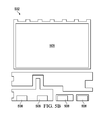
- FIG. 1A is a top-down view of an illustrative lead frame having multiple holes.
- FIG. 1B is a bottom-up view of the lead frame of FIG. 1A .
- FIG. 1C is a side view of the lead frame of FIG. 1A .
- FIG. 2A is a perspective view of the lead frame surface depicted in FIG. 1A .
- FIG. 2B is a perspective view of the lead frame surfaces depicted in FIG. 1B .
- FIG. 3 is a side view of a lead frame having a hole formed therein and a die and die attach material positioned thereupon.
- FIG. 4A is a top-down view of a portion of a lead frame having multiple holes and die attach material deposited thereupon.
- FIGS. 4B and 4C are top-down views of the portion of the lead frame depicted in FIG. 4A , with the die attach material having been reflowed.
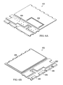
- FIG. 5A is a top-down view of an illustrative lead frame having multiple dimples.
- FIG. 5B is a bottom-up view of the lead frame of FIG. 5A .
- FIG. 6A is a perspective view of the lead frame surface depicted in FIG. 5A .
- FIG. 6B is a perspective view of the lead frame surfaces depicted in FIG. 5B .
- FIG. 7 is a side view of a lead frame having a dimple formed therein and a die and die attach material positioned thereupon.
- FIGS. 8A and 8C are top-down views of portions of lead frames having dimples and die attach material deposited thereupon.
- FIGS. 8B and 8D are top-down views of the portions of lead frames depicted in FIGS. 8A and 8C , respectively, with the die attach material having been reflowed.
- FIGS. 9A-9E are perspective views of an illustrative lead frame die attach and clip bonding process, in accordance with various embodiments.
- FIG. 10 is a flow diagram of an illustrative process in accordance with various embodiments.
- lead frames having holes, dimples, or both formed therein to control the flow of die attach material (e.g., epoxy, polyimide, silicone or hybrid organic adhesives, soft or eutectic solders).
- die attach material e.g., epoxy, polyimide, silicone or hybrid organic adhesives, soft or eutectic solders.
- FIG. 1A is a top-down view of an illustrative lead frame 102 .
- Lead frames are often composed of copper or copper-based alloys and are used to incorporate electronics—for example, integrated circuits and discrete devices (e.g., transistors, diodes)—into protective packages.
- the lead frames enable electrical signals to flow between the electronic device encapsulated within the package and electronic devices, such as a printed circuit board, outside the package.
- the lead frame 102 depicted in FIG. 1A and, more generally, the lead frames depicted in any portion of this disclosure do not limit the scope of this disclosure.
- the holes and dimples described herein may be formed in any suitable type of lead frame to control the flow of die attach material.
- the lead frame 102 comprises multiple holes 104 .
- the holes 104 pass through the thickness of the lead frame 102 such that the apertures of each hole are on opposing surfaces of the lead frame 102 .
- the holes 104 may be of any suitable diameter (e.g., a range of 0.1270 to 0.3048 mm, inclusive) depending on material thickness to achieve a through hole during the etching process, and may be formed in any suitable number, arrangement, and pitch.
- the holes 104 are arranged between the area in which die attach material (e.g., solder) is to be deposited and the area that is to be protected from die attach material flow.
- die attach material e.g., solder
- the holes 104 may be formed in any suitable area of the lead frame 102 , including leads, die flags, etc.
- the holes 104 preferably are formed during the lead frame etching process. Their sizes, quantities, and locations are determined by the masks used during the etching process.
- the holes 104 draw the die attach material toward themselves and away from the areas to be protected from the reflowed die attach material.
- the lead frame 102 includes at least one trench 106 .
- one purpose of the trench 106 is to control the flow of die attach material.
- the trench 106 does not pass completely through the thickness of the lead frame 102 .
- die attach material such as solder
- it approaches the trench 106 but—due to its tensile properties—does not enter the trench 106 .
- Its resistance to flowing into the trench 106 helps maintain the desired position of the die or other component that is coupled to the die attach material.
- the trench 106 controls the flow of the die attach material and, because the die attach material flow is controlled, the die that is coupled to the die attach material is precluded from sliding or moving into undesirable positions. Instead, the die remains in its proper position.
- FIG. 1B is a bottom-up view of the lead frame 102 of FIG. 1A .
- This view of the lead frame 102 depicts the holes 104 , since—as explained above—the holes 104 pass completely through the lead frame 102 .
- this view does not depict the trench 106 , since—as explained—the trench 106 does not pass completely through the lead frame 102 .
- the holes 104 are formed on areas of the lead frame 102 that have been half-etched.
- half-etched refers to a degree of etching that causes an area of a lead frame 102 to be approximately half the thickness (i.e., between 25 and 75%, inclusive) of another, non-half-etched area of the lead frame (depicted as numerals 108 in FIG. 1B ).
- the trench 106 is formed on an area of the top surface of the lead frame ( FIG. 1A ) that is opposite an area of the bottom surface that is not half-etched—e.g., one of the areas 108 , as shown.
- the holes 104 though formed in half-etched areas, do not compromise the structural integrity of the lead frame because they are comparatively small and are separated from each other.
- FIG. 1C is a side view of the lead frame 102 of FIG. 1A from the perspective of numerals 110 .
- the thickness of the lead frame 102 in areas that have been half-etched (marked as numeral 112 ) is approximately half that of areas that have not been half-etched (marked as numeral 108 ).
- FIG. 2A is a perspective view of the lead frame surface depicted in FIG. 1A
- FIG. 2B is a perspective view of the lead frame surfaces depicted in FIG. 1B .
- FIG. 3 is a side view of an illustrative lead frame 300 having a hole 302 formed in a half-etched area 304 and further having a die 306 and die attach material 308 positioned thereupon.
- the lead frame 300 also comprises a non-half-etched area 310 .
- the die attach material 308 and, more generally, any die attach material described herein may comprise epoxy, polyimide, silicone or hybrid organic adhesives, and/or soft or eutectic solders, and it may be deposited in gel, paste, film, tape, or solder form. Any such die attach material, when reflowed, may be referred to herein as “fluid,” irrespective of the viscosity of the material.
- FIG. 4A is a top-down view of a portion of an illustrative lead frame 400 having multiple holes 402 and die attach material 404 deposited thereupon (e.g., printed solder).
- the die attach material 404 is caused to flow—for instance, by a reflow process. As a result, the die attach material 404 may flow and eventually settle as depicted in FIG. 4B , which shows the material 404 partially encircling the holes 402 . The tensile characteristics of the die attach material 404 preclude the material 404 between the holes from flowing substantially beyond the area of the holes.
- FIG. 4C is another top-down view of the portion of the lead frame 400 depicted in FIG. 4A , with the die attach material 404 having been reflowed in a different pattern. As shown, the material 404 straddles the holes 402 without substantially entering the holes 402 , or, in some cases, without entering the holes 402 more than approximately halfway. Various such flow patterns are possible depending on a variety of factors, but in each case, the holes 402 effectively control solder flow and thus mitigate electrical shorts and/or poor electrical connections.
- FIG. 5A is a top-down view of an illustrative lead frame 502 having multiple dimples 504 .
- Dimples differ from holes in that they do not pass completely through the lead frame on which they are formed. Additionally, they may be smaller in diameter than holes, since the etching process generally will etch less deeply when the aperture diameter is smaller.
- the specific aperture diameter threshold above which a particular etching process will create a hole rather than a dimple is application-specific.
- the dimples 504 can be created in any suitable number, arrangement, pitch, location, size, and shape. For example, holes and dimples may be etched as semi-circles, ovals, rectangles, and the like.
- the typical dimple 504 will have an aperture diameter ranging between 0.0254 mm and 0.1016 mm, inclusive, depending on material thickness, although the scope of this disclosure is not limited as such.
- the lead frame 502 may additionally include a trench 506 .
- FIG. 5B is a bottom-up view of the lead frame 502 of FIG. 5A .
- the dimples 504 are formed in half-etched areas (as opposed to non-half-etched areas 508 ), but because the dimples 504 do not pass through the lead frame, they are not visible in FIG. 5B .
- the scope of disclosure is not limited to forming dimples only in half-etched areas; dimples may be formed in non-half-etched areas 508 .
- FIGS. 6A and 6B show perspective views of the lead frame 502 depicted in FIGS. 5A and 5B .
- FIG. 7 is a side view of an illustrative lead frame 700 having a dimple 702 formed therein and a die 708 and die attach material 706 positioned thereupon.
- the dimple 702 is formed in a half-etched area 704
- the lead frame 700 also includes a non-half-etched area 710 .
- the die attach material 706 is deposited directly into or over the dimple 702 . When the die attach material 706 is reflowed, it fills the dimple 702 .
- a sufficient amount of die attach material 706 is preferably deposited so that it fills the dimple 702 and overflows outside the dimple 702 so that a proper electrical connection may be formed with the die 708 .
- the scope of disclosure is not limited to using the dimple 702 as shown.
- the dimple 702 may be used as the hole 302 is used in FIG. 3 , meaning that the die attach material is deposited adjacent to the dimple 702 and permitted to flow toward the dimple 702 .
- the dimple 702 together with the tensile properties of the die attach material and any other dimples that may be positioned in the vicinity of the dimple 702 , preclude the die attach material from flowing substantially beyond the dimple(s).
- FIG. 8A is a top-down view of a portion of a lead frame 800 having a dimple 802 and die attach material 804 thereupon. As shown, the die attach material is printed or otherwise deposited directly on or above the dimple 802 . When reflowed, the die attach material 804 may flow in the pattern shown in FIG. 8B . In FIG. 8B , the die attach material 804 fills some or all of the dimple 802 .
- FIG. 8C is another top-down view of a portion of the lead frame 800 having a dimple 802 and die attach material 804 deposited thereupon. In FIG. 8C , the die attach material 804 is deposited adjacent to, rather than on top of, the dimple 802 .
- FIG. 8A is a top-down view of a portion of a lead frame 800 having a dimple 802 and die attach material 804 thereupon.
- the die attach material 804 is deposited adjacent to, rather than on top of, the dimple 802 .
- FIG. 8D shows the flow pattern of the die attach material 804 when reflowed.
- the reflowed die attach material 804 encircles at least part of the dimple aperture and may at least partially fill the dimple 802 .
- the scope of disclosure is not limited to any particular flow pattern, and no particular flow pattern is guaranteed to result from any particular type or configuration of die attach material.
- the die attach material 804 in FIG. 8C when the die attach material 804 in FIG. 8C is reflowed, it may produce a flow pattern like that in FIG. 8B rather than that depicted in FIG. 8D . Any and all such variations are contemplated and fall within the scope of this disclosure.
- FIGS. 9A-9E are perspective views of an illustrative lead frame die attach and clip bonding process, in accordance with various embodiments.
- FIG. 9A depicts a lead frame 900 having a plurality of holes and/or dimples 902 and a trench 904 .
- the holes and/or dimples 902 are etched at the same time that the lead frame 900 is etched using the appropriate mask(s).
- FIG. 9B depicts die attach material 906 having been deposited adjacent to, or directly on, the holes and/or dimples 902 .
- FIG. 9C depicts multiple die 908 being positioned on the lead frame 900 .
- the trench 904 can help one of the die 908 maintain proper position and prevent the die from sliding, and so one of the die 908 is positioned along the trench 904 , as shown.
- FIG. 9D shows additional die attach material 910 being deposited atop the multiple die 908 .
- FIG. 9E depicts clips 912 , 914 being coupled to the die attach material on the lead frame 900 and on the die 908 , as shown. This coupling establishes electrical connections between the lead frame 900 and the multiple die 908 .
- FIG. 9E depicts the clip 914 having multiple holes 916 , each of which is positioned to align with one or more depositions of die attach material 910 atop the die 908 .
- the die attach material 910 atop the die 908 flows through the holes 916 instead of being squeezed out from between the edges of the die 908 and the clip 914 . Due to these holes 916 , the clip 914 —like the die 908 —remains in position and does not slide.
- dimples may be formed in the clip 914 in addition to, or in lieu of, the holes 916 .
- FIG. 10 is a flow diagram of an illustrative process 1000 in accordance with various embodiments.
- the process 1000 begins by etching at least a portion of a first surface of a lead frame (step 1002 ). This step includes half-etching at least a portion of the first surface.
- the process 1000 continues by etching one or more holes or dimples on a second surface of the lead frame (step 1004 ).
- the lead frame may have holes, dimples, or a combination thereof.
- the holes preferably are formed in areas that have been half-etched so that the holes pass completely through the lead frame.
- Dimples preferably are formed in half-etched areas as well. The scope of disclosure, however, includes forming dimples in non-half-etched areas.
- the process 1000 also includes applying die attach material on the second surface of the lead frame in selectively targeted areas (step 1006 ).
- the die attach material is then reflowed, and the flow of the die attach material is controlled by the holes and/or dimples (step 1008 ).
- the method 1000 may be modified by adding, removing, modifying, or rearranging one or more steps.
Landscapes
- Lead Frames For Integrated Circuits (AREA)
Abstract
Description
Claims (18)
Priority Applications (2)
| Application Number | Priority Date | Filing Date | Title |
|---|---|---|---|
| US15/240,423 US9911684B1 (en) | 2016-08-18 | 2016-08-18 | Holes and dimples to control solder flow |
| CN201721027383.7U CN207818564U (en) | 2016-08-18 | 2017-08-17 | system for lead frame |
Applications Claiming Priority (1)
| Application Number | Priority Date | Filing Date | Title |
|---|---|---|---|
| US15/240,423 US9911684B1 (en) | 2016-08-18 | 2016-08-18 | Holes and dimples to control solder flow |
Publications (2)
| Publication Number | Publication Date |
|---|---|
| US20180053712A1 US20180053712A1 (en) | 2018-02-22 |
| US9911684B1 true US9911684B1 (en) | 2018-03-06 |
Family
ID=61192122
Family Applications (1)
| Application Number | Title | Priority Date | Filing Date |
|---|---|---|---|
| US15/240,423 Active 2036-08-28 US9911684B1 (en) | 2016-08-18 | 2016-08-18 | Holes and dimples to control solder flow |
Country Status (2)
| Country | Link |
|---|---|
| US (1) | US9911684B1 (en) |
| CN (1) | CN207818564U (en) |
Families Citing this family (5)
| Publication number | Priority date | Publication date | Assignee | Title |
|---|---|---|---|---|
| DE102018128109A1 (en) | 2018-11-09 | 2020-05-14 | Infineon Technologies Ag | A CLIP WITH A FASTENING SECTION CONFIGURED TO PROMOTE THE REMOVAL OF CAVES IN SOLDERING |
| US11211353B2 (en) | 2019-07-09 | 2021-12-28 | Infineon Technologies Ag | Clips for semiconductor packages |
| CN110364503B (en) * | 2019-07-25 | 2020-11-27 | 珠海格力电器股份有限公司 | A novel leadless chip package structure and its manufacturing method |
| JP7292352B2 (en) * | 2021-11-02 | 2023-06-16 | 三菱電機株式会社 | Resin-encapsulated semiconductor device and method for manufacturing resin-encapsulated semiconductor device |
| US20250201681A1 (en) * | 2023-12-18 | 2025-06-19 | Semiconductor Components Industries, Llc | Wire bonding using a floating pad |
Citations (17)
| Publication number | Priority date | Publication date | Assignee | Title |
|---|---|---|---|---|
| US6235556B1 (en) * | 1998-07-06 | 2001-05-22 | Clear Logic, Inc. | Method of improving parallelism of a die to package using a modified lead frame |
| US6448507B1 (en) * | 2000-06-28 | 2002-09-10 | Advanced Micro Devices, Inc. | Solder mask for controlling resin bleed |
| US6521982B1 (en) * | 2000-06-02 | 2003-02-18 | Amkor Technology, Inc. | Packaging high power integrated circuit devices |
| US20050236701A1 (en) * | 2002-10-24 | 2005-10-27 | Matsushita Electric Industrial Co., Ltd. | Leadframe, plastic-encapsulated semiconductor device, and method for fabricating the same |
| US7081666B2 (en) * | 2003-04-11 | 2006-07-25 | Fairchild Semiconductor Corporation | Lead frame structure with aperture or groove for flip chip in a leaded molded package |
| US20070114352A1 (en) * | 2005-11-18 | 2007-05-24 | Victor R Cruz Erwin | Semiconductor die package using leadframe and clip and method of manufacturing |
| US20070241432A1 (en) * | 2005-08-09 | 2007-10-18 | Il Kwon Shim | Etched leadframe flipchip package system |
| US7972906B2 (en) * | 2008-03-07 | 2011-07-05 | Fairchild Semiconductor Corporation | Semiconductor die package including exposed connections |
| US20110193208A1 (en) * | 2008-03-31 | 2011-08-11 | Yan Xun Xue | Semiconductor package of a flipped mosfet and its manufacturing method |
| US7999281B2 (en) * | 2006-10-18 | 2011-08-16 | Kabushiki Kaisha Toshiba | Optical semiconductor device and method of manufacturing optical semiconductor device |
| US20110298116A1 (en) * | 2010-06-03 | 2011-12-08 | Renesas Electronics Corporation | Semiconductor device and production method thereof |
| US20130009295A1 (en) * | 2011-07-06 | 2013-01-10 | Infineon Technologies Ag | Semiconductor Device Including a Contact Clip Having Protrusions and Manufacturing Thereof |
| US20130009297A1 (en) * | 2008-04-04 | 2013-01-10 | Gem Services, Inc. | Semiconductor device package having configurable lead frame fingers |
| US20150054147A1 (en) * | 2012-12-20 | 2015-02-26 | Intersil Americas LLC | Lead frame having a perimeter recess within periphery of component terminal |
| US8982577B1 (en) * | 2012-02-17 | 2015-03-17 | Amkor Technology, Inc. | Electronic component package having bleed channel structure and method |
| US9214440B1 (en) * | 2014-12-17 | 2015-12-15 | Texas Instruments Incorporated | Method for preventing die pad delamination |
| US20160358843A1 (en) * | 2015-06-03 | 2016-12-08 | Infineon Technologies Ag | Semiconductor device including a clip |
-
2016
- 2016-08-18 US US15/240,423 patent/US9911684B1/en active Active
-
2017
- 2017-08-17 CN CN201721027383.7U patent/CN207818564U/en active Active
Patent Citations (17)
| Publication number | Priority date | Publication date | Assignee | Title |
|---|---|---|---|---|
| US6235556B1 (en) * | 1998-07-06 | 2001-05-22 | Clear Logic, Inc. | Method of improving parallelism of a die to package using a modified lead frame |
| US6521982B1 (en) * | 2000-06-02 | 2003-02-18 | Amkor Technology, Inc. | Packaging high power integrated circuit devices |
| US6448507B1 (en) * | 2000-06-28 | 2002-09-10 | Advanced Micro Devices, Inc. | Solder mask for controlling resin bleed |
| US20050236701A1 (en) * | 2002-10-24 | 2005-10-27 | Matsushita Electric Industrial Co., Ltd. | Leadframe, plastic-encapsulated semiconductor device, and method for fabricating the same |
| US7081666B2 (en) * | 2003-04-11 | 2006-07-25 | Fairchild Semiconductor Corporation | Lead frame structure with aperture or groove for flip chip in a leaded molded package |
| US20070241432A1 (en) * | 2005-08-09 | 2007-10-18 | Il Kwon Shim | Etched leadframe flipchip package system |
| US20070114352A1 (en) * | 2005-11-18 | 2007-05-24 | Victor R Cruz Erwin | Semiconductor die package using leadframe and clip and method of manufacturing |
| US7999281B2 (en) * | 2006-10-18 | 2011-08-16 | Kabushiki Kaisha Toshiba | Optical semiconductor device and method of manufacturing optical semiconductor device |
| US7972906B2 (en) * | 2008-03-07 | 2011-07-05 | Fairchild Semiconductor Corporation | Semiconductor die package including exposed connections |
| US20110193208A1 (en) * | 2008-03-31 | 2011-08-11 | Yan Xun Xue | Semiconductor package of a flipped mosfet and its manufacturing method |
| US20130009297A1 (en) * | 2008-04-04 | 2013-01-10 | Gem Services, Inc. | Semiconductor device package having configurable lead frame fingers |
| US20110298116A1 (en) * | 2010-06-03 | 2011-12-08 | Renesas Electronics Corporation | Semiconductor device and production method thereof |
| US20130009295A1 (en) * | 2011-07-06 | 2013-01-10 | Infineon Technologies Ag | Semiconductor Device Including a Contact Clip Having Protrusions and Manufacturing Thereof |
| US8982577B1 (en) * | 2012-02-17 | 2015-03-17 | Amkor Technology, Inc. | Electronic component package having bleed channel structure and method |
| US20150054147A1 (en) * | 2012-12-20 | 2015-02-26 | Intersil Americas LLC | Lead frame having a perimeter recess within periphery of component terminal |
| US9214440B1 (en) * | 2014-12-17 | 2015-12-15 | Texas Instruments Incorporated | Method for preventing die pad delamination |
| US20160358843A1 (en) * | 2015-06-03 | 2016-12-08 | Infineon Technologies Ag | Semiconductor device including a clip |
Also Published As
| Publication number | Publication date |
|---|---|
| US20180053712A1 (en) | 2018-02-22 |
| CN207818564U (en) | 2018-09-04 |
Similar Documents
| Publication | Publication Date | Title |
|---|---|---|
| US9911684B1 (en) | Holes and dimples to control solder flow | |
| US9640465B2 (en) | Semiconductor device including a clip | |
| DE102015115999B4 (en) | Electronic component | |
| JP3080607B2 (en) | Method of controlling solder bump shape and standoff height | |
| CN104427782B (en) | Electronic installation | |
| US8524531B2 (en) | System and method for improving solder joint reliability in an integrated circuit package | |
| DE10392228T5 (en) | Semiconductor chip package with semiconductor chip with side electrical connection | |
| DE102011113269A1 (en) | Semiconductor module and method for its production | |
| US9627297B2 (en) | Solder flow-impeding plug on a lead frame | |
| CN101276798A (en) | Isolated Solder Pads | |
| US20190252347A1 (en) | Trace Design for Bump-on-Trace (BOT) Assembly | |
| JP2016092138A5 (en) | ||
| DE102010016517A1 (en) | Semiconductor device | |
| DE10148463A1 (en) | Method and device for producing a metallic bump with increased height | |
| US20170053883A1 (en) | Integrated circuit package | |
| US9165867B1 (en) | Semiconductor device with lead frame contact solder balls and related methods | |
| US10546805B2 (en) | Integrated circuit package with conductive clips | |
| US9368433B2 (en) | Method and apparatus for mounting solder balls to an exposed pad or terminal of a semiconductor package | |
| US20250105105A1 (en) | Semiconductor device | |
| EP3024025A1 (en) | Die arrangement | |
| JP2006237367A (en) | Printed wiring board | |
| US20060234490A1 (en) | Increased stand-off height integrated circuit assemblies, systems, and methods | |
| DE102006024943A1 (en) | A design and method for mounting a die on a leadframe in a semiconductor device | |
| JP6345554B2 (en) | Printed wiring board | |
| JP2006049528A (en) | Semiconductor device and manufacturing method of semiconductor device |
Legal Events
| Date | Code | Title | Description |
|---|---|---|---|
| AS | Assignment |
Owner name: SEMICONDUCTOR COMPONENTS INDUSTRIES, LLC, ARIZONA Free format text: ASSIGNMENT OF ASSIGNORS INTEREST;ASSIGNORS:ST. GERMAIN, STEPHEN;CONNER, DENNIS LEE;YODER, JAY A.;SIGNING DATES FROM 20160817 TO 20160818;REEL/FRAME:039476/0517 |
|
| AS | Assignment |
Owner name: DEUTSCHE BANK AG NEW YORK BRANCH, NEW YORK Free format text: SECURITY INTEREST;ASSIGNOR:SEMICONDUCTOR COMPONENTS INDUSTRIES, LLC;REEL/FRAME:041187/0295 Effective date: 20161221 |
|
| STCF | Information on status: patent grant |
Free format text: PATENTED CASE |
|
| MAFP | Maintenance fee payment |
Free format text: PAYMENT OF MAINTENANCE FEE, 4TH YEAR, LARGE ENTITY (ORIGINAL EVENT CODE: M1551); ENTITY STATUS OF PATENT OWNER: LARGE ENTITY Year of fee payment: 4 |
|
| AS | Assignment |
Owner name: FAIRCHILD SEMICONDUCTOR CORPORATION, ARIZONA Free format text: RELEASE OF SECURITY INTEREST IN PATENTS RECORDED AT REEL 041187, FRAME 0295;ASSIGNOR:DEUTSCHE BANK AG NEW YORK BRANCH, AS COLLATERAL AGENT;REEL/FRAME:064151/0203 Effective date: 20230622 Owner name: SEMICONDUCTOR COMPONENTS INDUSTRIES, LLC, ARIZONA Free format text: RELEASE OF SECURITY INTEREST IN PATENTS RECORDED AT REEL 041187, FRAME 0295;ASSIGNOR:DEUTSCHE BANK AG NEW YORK BRANCH, AS COLLATERAL AGENT;REEL/FRAME:064151/0203 Effective date: 20230622 |
|
| MAFP | Maintenance fee payment |
Free format text: PAYMENT OF MAINTENANCE FEE, 8TH YEAR, LARGE ENTITY (ORIGINAL EVENT CODE: M1552); ENTITY STATUS OF PATENT OWNER: LARGE ENTITY Year of fee payment: 8 |