US9906122B2 - Methods to reduce current spikes in capacitive DC-DC converters employing gain-hopping - Google Patents
Methods to reduce current spikes in capacitive DC-DC converters employing gain-hopping Download PDFInfo
- Publication number
- US9906122B2 US9906122B2 US13/856,393 US201313856393A US9906122B2 US 9906122 B2 US9906122 B2 US 9906122B2 US 201313856393 A US201313856393 A US 201313856393A US 9906122 B2 US9906122 B2 US 9906122B2
- Authority
- US
- United States
- Prior art keywords
- switched capacitor
- capacitor array
- gain
- control
- voltage
- Prior art date
- Legal status (The legal status is an assumption and is not a legal conclusion. Google has not performed a legal analysis and makes no representation as to the accuracy of the status listed.)
- Expired - Fee Related, expires
Links
Images


Classifications
-
- H—ELECTRICITY
- H02—GENERATION; CONVERSION OR DISTRIBUTION OF ELECTRIC POWER
- H02M—APPARATUS FOR CONVERSION BETWEEN AC AND AC, BETWEEN AC AND DC, OR BETWEEN DC AND DC, AND FOR USE WITH MAINS OR SIMILAR POWER SUPPLY SYSTEMS; CONVERSION OF DC OR AC INPUT POWER INTO SURGE OUTPUT POWER; CONTROL OR REGULATION THEREOF
- H02M3/00—Conversion of dc power input into dc power output
- H02M3/02—Conversion of dc power input into dc power output without intermediate conversion into ac
- H02M3/04—Conversion of dc power input into dc power output without intermediate conversion into ac by static converters
- H02M3/06—Conversion of dc power input into dc power output without intermediate conversion into ac by static converters using resistors or capacitors, e.g. potential divider
- H02M3/07—Conversion of dc power input into dc power output without intermediate conversion into ac by static converters using resistors or capacitors, e.g. potential divider using capacitors charged and discharged alternately by semiconductor devices with control electrode, e.g. charge pumps
Definitions
- the present disclosure relates to capacitive DC-DC converters, and more specifically to a system and method to reduce current spikes in capacitive DC-DC converters that employ gain hopping.
- Capacitive DC-DC voltage converters are known in the art. Although such voltage converters have known advantages for integrated circuit applications, they also have known disadvantages, such as limited capability to drive high current loads.
- a capacitive voltage converter providing multiple gain modes comprising a switched capacitor array having a voltage input and a voltage output.
- a skip gating control coupled to the switched capacitor array and configured to control a switch resistance value of the switched capacitor array, and to control a switching sequence of the switched capacitor array.
- An override control coupled to the skip gating control and the switched capacitor array, the override control configured to detect transitions in a gain mode and to modify the switch resistance value of the switched capacitor array and the switching sequence of the switched capacitor array for a finite amount of time following the gain mode transition.
- FIG. 1 is a diagram of a system for a capacitive dc-dc converter with variable input and output voltages in accordance with an exemplary embodiment of the present disclosure
- FIG. 2 is a diagram showing gain modes as a function of voltage in accordance with an exemplary embodiment of the present disclosure
- FIG. 3 is a diagram of a current response and of an efficiency response of a system in accordance with an exemplary embodiment of the present disclosure
- FIGS. 4A and 4B are flow charts of an algorithm for controlling a mode of operation of a DC-DC converter in accordance with an exemplary embodiment of the present disclosure
- FIG. 5 is a diagram showing the effect of R SW on current in accordance with an exemplary embodiment of the present invention.
- FIG. 6 is a diagram of capacitor configurations for phase transitions in accordance with an exemplary embodiment of the present invention.
- FIG. 7 is a diagram showing current overshoot and reverse flow conditions that can occur with uncorrected phase transitions
- FIG. 8 is a diagram showing current response when applying an override system in accordance with an exemplary embodiment of the present invention.
- FIG. 9 is a diagram showing current flow as a function of phase and gain mode in accordance with an exemplary embodiment of the present disclosure.
- Capacitive DC-DC converters (“charge-pumps”) are becoming increasingly common for generation of ASIC power supplies at low or moderate current levels. Because they require no external inductive components, they offer an inexpensive bill of materials, a small footprint, and limited electromagnetic interference concerns.
- a control loop can be used for capacitive DC-DC converters to regulate the charge-pump output voltage. While “skip mode” regulation (which consists in stopping the charge-pump switching activity when the output voltage exceeds the target voltage) and “gain hopping” regulation (which dynamically adjusts charge-pump gain as a function of input voltage, output voltage and loading conditions) are known, skip mode regulation without gain control is very inefficient if the input voltage varies over wide voltage ranges, and gain hopping involves significant power losses at the transitions between low and high gain and is only effective for certain combinations of input and output voltages.
- a skip comparator stops switching activity in a capacitor array whenever the output voltage exceeds the target voltage plus a small overhead voltage ⁇ V.
- a hop comparator selects one of two gain modes for the switched cap array: a higher gain that is used when V OUT is less than V TARGET , and a lower gain that is used when V OUT is greater than V TARGET .
- gain modes are utilized.
- four gain modes are utilized, namely:
- the current flowing into the charge pump at any given time is proportional to ((G ⁇ V IN ) ⁇ V OUT )/R SW , where G is the charge-pump gain and R SW is the resistance of the switched capacitor array. While R SW should be kept sufficiently low in order for the charge-pump to be able to deliver the largest required output current in the worst-case conditions for V IN /V OUT (such as when ((G ⁇ V IN ) ⁇ V OUT ) is small), under more favorable conditions (such as when ((G ⁇ V IN ) ⁇ V OUT ) is large) a small value of R SW can cause unnecessarily high current peaks and does not improve the overall power efficiency.
- R SW selection table In order to reduce current peaks, an “R SW selection table” is introduced. This table is used to compute ((G ⁇ V IN ) ⁇ V TARGET )) by combining the A/D outputs and gain mode information (D 0 -D 3 ) to select a higher value for the R SW parameter when possible.
- R SW can be modulated in discrete steps by splitting each switch of the capacitor array into an array of smaller switches, each providing a resistance multiple of R SW .
- switch resistance is not a constant but varies as a function of V IN in a non-linear manner.
- the switches can be driven much more efficiently (lower resistance) at a higher voltage than at a lower voltage.
- the dependence of R SW on V IN can also be included in the lookup table without any further hardware requirements, as only the content of the lookup table needs to be updated. In this manner, the charge-pump can take full advantage of the lower resistance available at higher V IN when necessary, while properly scaling the switch resistance up when possible.
- the skip gating block consists of one AND gate for each switch control signal.
- the gain selection logic is relatively simple digital combinational logic.
- the lookup table is quite small in size.
- each ADC is 3-bit resolution and the table stores 128 ⁇ 3-bit words.
- the analog to digital converter (ADC) used for V IN can be of low resolution, such as a 3-bit ADC, with minimal impact to the overall efficiency curve.
- a second ADC block connected to V TARGET is usually unnecessary as the V TARGET information is already available in digital format for a charge-pump with programmable output voltage.
- the disclosed SHL mode uses two comparators instead of one in order to decouple the hop control from the skip control.
- the charge pump gain is increased as soon as the skip duty ratio exceeds 80% so the charge pumps ends up working in a higher gain setting more frequently than is necessary, which causes a drop in efficiency.
- Using two comparators allows the charge-pump to stay in skip mode (at a lowest gain setting) even as the duty ratio approaches 100%.
- switch resistance control is added to the control loop.
- An analog feedback loop for switch resistance control is replaced with an open-loop discrete control, to eliminate analog components from the design (filter, variable-resistance switches), and to allow co-existence with gain-hopping.
- FIG. 1 is a diagram of a system 100 for a capacitive dc-dc converter with variable input and output voltages in accordance with an exemplary embodiment of the present disclosure.
- System 100 can be implemented in hardware or a suitable combination of hardware and software, and can be one or more software systems operating on a hardware platform.
- “hardware” can include a combination of discrete components, an integrated circuit, an application-specific integrated circuit, a field programmable gate array, or other suitable hardware.
- “software” can include one or more objects, agents, threads, lines of code, subroutines, separate software applications, two or more lines of code or other suitable software structures operating in two or more software applications or on two or more processors, or other suitable software structures.
- software can include one or more lines of code or other suitable software structures operating in a general purpose software application, such as an operating system, and one or more lines of code or other suitable software structures operating in a specific purpose software application.
- Switched capacitor array 102 is a suitable combination of series and/or parallel connected switched capacitors that allows the values of the resistance and the topology of the switched-capacitor network to be controllably modified.
- switched capacitor array 102 can be the combination of series and parallel connected switched capacitors shown in FIG. 4.5 of “Design of High Efficiency Step-Down Switched Capacitor DC/DC Converter,” Mengzhe Ma, Oregon State University (May 21, 2003), which is hereby incorporated by reference, or other suitable switched capacitor arrays.
- Switched capacitor array 102 receives input voltage V IN and outputs voltage V OUT .
- the current consumed by switched capacitor array 102 and the efficiency of switched capacitor array 102 can be controlled, so as to minimize the current consumed and to maximize the efficiency.
- Controls for selecting switches that control the resistance and capacitor settings of switched capacitor array 102 are received from R SW selection table 104 and skip gating 106 .
- R SW selection table 104 is used to select values of resistance for switched capacitor array 102
- skip gating 106 is used to control topology and switching activity for switched capacitor array 102
- R SW selection table 104 receives inputs representing the target voltage V TARGET from analog to digital converter 112 , the input voltage V IN from analog to digital converter 110 and the gain mode control signal from gain selection logic 108 , and generates a resistor selection setting as a function of those inputs.
- An example of values for R SW selection table 104 is provided below. The values range from 1 ohm to 8 ohms, and higher resistance values are chosen when V IN is larger.
- This exemplary lookup table can be selected when the gain mode is D 3 , with similar tables being used for each of the other gain modes (such as D 0 , D 1 and D 2 ).
- Gain selection logic 108 receives an input representing target voltage V TARGET from analog to digital converter 112 , an input representing input voltage V IN from analog to digital converter 110 and the output of comparator 116 , which receives V TARGET and V OUT and which generates and output indicative of whether V TARGET is larger or smaller than V OUT .
- Gain selection logic 108 outputs a control signal to R SW selection table 104 and skip gating 106 indicating which gain region the system should be operating in (D 0 through D 3 ).
- Skip gating 106 receives the output from gain selection logic 108 and a signal from comparator 114 , which compares V OUT and V TARGET plus a small overhead voltage ⁇ V.
- Capacitor 118 is coupled to the output V OUT in order to reduce voltage ripple.
- Override 120 is used to alter the normal switching activity to reduce current spikes.
- One problem associated with gain-hopping is that the voltage on the fly capacitors has to change as the mode of operation changes. A sudden voltage change results in several problems:
- the steady-state voltage on the fly capacitors is approximately Vin/3.
- the steady-state voltage on the fly capacitors is V IN /2.
- the two fly capacitors are connected in series and try to drive V OUT to 0 V. Since the bulk capacitor on V OUT is already charged to V IN /3, a large current spike will flow out of V OUT and into V IN as shown in FIG. 9 .
- FIG. 9 when transitioning from state D 2 to state D 3 , it is better to be in phase two to avoid current spikes on V IN . Likewise, in a transition from D 3 to D 2 , it is better to be in phase one.
- override 120 alters the PH 1 -PH 2 switching pattern shown in FIG. 6 immediately after the gain transition. For instance, one of the two phases can be forced for a certain number of cycles to allow the capacitors to change their voltage in the most favorable state (i.e. avoid drawing currents from the output node), such as by overriding a clock signal that is provided to the capacitor switches for a predetermined number of clock cycles.
- override 120 alters the normal switch resistance immediately after the gain transition. For instance, the switch resistance can be increased for a certain number of clock cycles to reduce the magnitude of the current spikes.
- the switch matrix when transitioning from D 2 to D 3 , the switch matrix is forced to PH 2 for a predetermined number of clock cycles, such as 4 clock cycles, until the capacitor voltage is close to V DD /3.
- the switch resistance can be increased by a suitable amount, such as a factor of 3, for a predetermined number of clock cycles, such as two clock cycles.
- the charge pump switched capacitor DC-DC converter
- the charge pump is controlled to hop between the minimum gain and a higher gain, so that the charge pump can deliver enough charge to support a large load current at a desired output voltage without significantly reducing the efficiency.
- the charge pump runs at a lower gain for a few clock cycles, and runs at a higher gain for another few clock cycles. Consequently, the converter keeps hopping between different gains to make the average gain as low as possible to maximize the efficiency.
- the clock signal can be forced high in one of the phases, long enough to pre-charge the fly capacitors to the most appropriate voltage, so that when the next phase arrives, the current spike is lower than cases where the clock signal continues unmodified.
- system 100 provides for the combination of a skip mode control for a DC-DC converter (which is used for overall output voltage control and to achieve high-efficiency at light current loads) with gain hopping mode of operation for a DC-DC converter (which is used for high-efficiency over wide voltage ranges) and with a linear mode of operation for a DC-DC converter (which is used for controlling current spikes).
- System 100 thus provides for improved efficiency and reduced current requirements.
- FIG. 2 is a diagram 200 showing gain modes as a function of voltage in accordance with an exemplary embodiment of the present disclosure.
- Diagram 200 shows four exemplary gain modes that can be utilized to improve the efficiency of a DC-DC voltage converter, namely:
- FIG. 3 is a diagram of a current response 300 A and of an efficiency response 300 B of a system such as system 100 , in accordance with an exemplary embodiment of the present disclosure.
- Current response 300 A increases in magnitude as the efficiency response follows a gain curve downward with increasing input voltage, then reduces in magnitude in the region between gain curves.
- the switch resistance R SW of the switched capacitor bank By controlling the value of the switch resistance R SW of the switched capacitor bank, the current peak can be maintained at a level that is a factor of two or more less than the current peaks seen in prior art systems.
- FIGS. 4A and 4B are flow charts of algorithms 400 A and 400 B for controlling a mode of operation of a DC-DC converter in accordance with an exemplary embodiment of the present disclosure.
- Algorithms 400 A and 400 B can be implemented in hardware or a suitable combination of hardware and software, and can be one or more software systems operating on a hardware platform.
- Algorithm 400 A begins at 402 , where a value of V IN is received and digitized.
- the analog value of V IN can be received at an analog to digital converter and can be converted into a binary value representing the analog voltage magnitude.
- the algorithm then proceeds to 406 and 418 .
- an analog value of a target output voltage V TARGET is received and digitized.
- the analog value of V TARGET can be received at an analog to digital converter and can be converted into a binary value representing the analog voltage magnitude. The algorithm then proceeds to 406 and 418 .
- a gain region is selected, such as based on the value of V IN or other suitable variables.
- the algorithm then proceeds to 408 , the output voltage V OUT is compared to the target voltage V TARGET , such as by providing the voltages as inputs to a comparator and generating an output. If the value of V OUT is larger than the target voltage V TARGET , then the algorithm proceeds to 412 , where a low gain mode is selected, otherwise, the algorithm proceeds to 410 where a high gain mode is selected. The algorithm then proceeds to 418 , where a switch resistance is selected, and to 414 , where it is determined whether V OUT is greater than V TARGET plus a small overhead voltage ⁇ V. If V OUT is greater than V TARGET plus a small overhead voltage ⁇ V, the algorithm returns to 402 and 404 , otherwise, the algorithm proceeds to 416 , where switching activity is performed.
- Algorithm 400 B shares common elements with algorithm 400 A, but instead of 408 to 412 , provides 418 to 422 as described herein.
- algorithms 400 A and 400 B allow a capacitor array in a DC-DC converter to be controlled so as to improve efficiency, reduce current to the capacitor array, and for other suitable purposes.
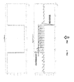
- FIG. 5 is a diagram 500 showing the effect of R SW on current in accordance with an exemplary embodiment of the present invention.
- the top line ( 502 ) shows an example of the current drawn as a function of voltage when the switch resistance uniformly equals 1 ohm
- the bottom line ( 504 ) shows an example of the current for the same voltage profile when the switch resistance is allowed to vary as described herein.
Abstract
Description
-
- mode D0 with a gain=1
- mode D1 with a gain=⅔
- mode D2 with a gain=½
- mode D3 with a gain=⅓
| TARGET | VIN |
| (volts) | <2.8 | 2.8-3.0 | 3.0-3.2 | 3.2-3.4 | 3.4-3.6 | >3.6 |
| 0.7-0.8 | 1 |
2 Ω | 4 Ω | 5 Ω | 6 Ω | 8 Ω |
| 0.8-0.9 | 1 Ω | 1 |
2 |
3 Ω | 5 Ω | 6 Ω |
| 0.9-1.0 | 1 Ω | 1 Ω | 1 Ω | 1 |
3 Ω | 5 Ω |
| 1.0-1.1 | 1 Ω | 1 Ω | 1 Ω | 1 Ω | 1 |
2 Ω |
-
- The presence of large current spikes on the input and output nodes as the fly capacitors are quickly charged/discharged. Current spikes can generate noise on the power/ground lines and impact performance for other components in the system.
- A loss of power efficiency as the large current flows through the (resistive) capacitor switches, as power dissipation equals I2×R.
- Supply pumping in the case of negative current spikes, as the current is being pushed into the input supply.
- EMI (conducted emissions).
| Force | Num of Clk | Switch | ||
| Gain Transition | phase | cycles | resisitance | |
| D0 → D1/D1 | None | 0 | No change | |
| D1 → | Ph1 | 2 | Increase by a | |
| factor N1 | ||||
| D2 → | No change | 0 | No change | |
| D2 → | Ph2 | 2 | Increase by a | |
| factor N1 | ||||
| D3 → | Ph1 | 2 | Increase by a | |
| factor N2 | ||||
-
- mode D0 with a gain=1
- mode D1 with a gain=⅔
- mode D2 with a gain=½
- mode D3 with a gain=⅓
Claims (15)
Priority Applications (1)
| Application Number | Priority Date | Filing Date | Title |
|---|---|---|---|
| US13/856,393 US9906122B2 (en) | 2012-04-03 | 2013-04-03 | Methods to reduce current spikes in capacitive DC-DC converters employing gain-hopping |
Applications Claiming Priority (2)
| Application Number | Priority Date | Filing Date | Title |
|---|---|---|---|
| US201261619845P | 2012-04-03 | 2012-04-03 | |
| US13/856,393 US9906122B2 (en) | 2012-04-03 | 2013-04-03 | Methods to reduce current spikes in capacitive DC-DC converters employing gain-hopping |
Publications (2)
| Publication Number | Publication Date |
|---|---|
| US20130257176A1 US20130257176A1 (en) | 2013-10-03 |
| US9906122B2 true US9906122B2 (en) | 2018-02-27 |
Family
ID=49233947
Family Applications (1)
| Application Number | Title | Priority Date | Filing Date |
|---|---|---|---|
| US13/856,393 Expired - Fee Related US9906122B2 (en) | 2012-04-03 | 2013-04-03 | Methods to reduce current spikes in capacitive DC-DC converters employing gain-hopping |
Country Status (1)
| Country | Link |
|---|---|
| US (1) | US9906122B2 (en) |
Cited By (2)
| Publication number | Priority date | Publication date | Assignee | Title |
|---|---|---|---|---|
| US11368132B2 (en) | 2019-12-26 | 2022-06-21 | Synaptics Incorporated | Low delay, low power and high linearity class-D modulation loop |
| US11594964B2 (en) | 2020-12-01 | 2023-02-28 | Synaptics Incorporated | DC-DC converter output regulation systems and methods |
Families Citing this family (6)
| Publication number | Priority date | Publication date | Assignee | Title |
|---|---|---|---|---|
| EP3111726A1 (en) | 2014-02-24 | 2017-01-04 | Philips Lighting Holding B.V. | Driver circuit with extended operation range |
| US9680371B2 (en) | 2014-04-24 | 2017-06-13 | Qualcomm Incorporated | Charge pumps having variable gain and variable frequency |
| US9276562B2 (en) | 2014-04-24 | 2016-03-01 | Qualcomm, Incorporated | Charge-recycling circuits including switching power stages with floating rails |
| US9525337B2 (en) | 2014-04-24 | 2016-12-20 | Qualcomm Incorporated | Charge-recycling circuits |
| CN104868706B (en) * | 2015-06-05 | 2017-07-18 | 南京航空航天大学 | A kind of charge pump DC-DC converter automatic gain saltus step control method |
| US10141832B2 (en) * | 2015-07-10 | 2018-11-27 | Maxim Integrated Products, Inc. | Systems and methods for reducing switch stress in switched mode power supplies |
Citations (3)
| Publication number | Priority date | Publication date | Assignee | Title |
|---|---|---|---|---|
| US6055168A (en) * | 1998-03-04 | 2000-04-25 | National Semiconductor Corporation | Capacitor DC-DC converter with PFM and gain hopping |
| US7342389B1 (en) * | 2007-01-09 | 2008-03-11 | Diodes, Inc. | High efficiency charge pump DC to DC converter circuits and methods |
| US20130141071A1 (en) * | 2011-12-06 | 2013-06-06 | Matteo Conta | System and method for capacitive dc-dc converter with variable input and output voltages |
-
2013
- 2013-04-03 US US13/856,393 patent/US9906122B2/en not_active Expired - Fee Related
Patent Citations (3)
| Publication number | Priority date | Publication date | Assignee | Title |
|---|---|---|---|---|
| US6055168A (en) * | 1998-03-04 | 2000-04-25 | National Semiconductor Corporation | Capacitor DC-DC converter with PFM and gain hopping |
| US7342389B1 (en) * | 2007-01-09 | 2008-03-11 | Diodes, Inc. | High efficiency charge pump DC to DC converter circuits and methods |
| US20130141071A1 (en) * | 2011-12-06 | 2013-06-06 | Matteo Conta | System and method for capacitive dc-dc converter with variable input and output voltages |
Non-Patent Citations (3)
| Title |
|---|
| Bayer, Erich, et al.; "Charge Pump with Active Cycle Regulation-Closing the Gap between Linear-and Skip Modes;" 0-7803-5692-6 (c) 2000 IEEE; pp. 1497-1502. |
| Bayer, Erich, et al.; "Charge Pump with Active Cycle Regulation—Closing the Gap between Linear—and Skip Modes;" 0-7803-5692-6 (c) 2000 IEEE; pp. 1497-1502. |
| Ma, Mengzhe; "Design of High Efficiency Step-Down Switched Capacitor DC/DC Converter;" A Thesis Submitted to Oregon State University; Presented May 21, 2003. |
Cited By (2)
| Publication number | Priority date | Publication date | Assignee | Title |
|---|---|---|---|---|
| US11368132B2 (en) | 2019-12-26 | 2022-06-21 | Synaptics Incorporated | Low delay, low power and high linearity class-D modulation loop |
| US11594964B2 (en) | 2020-12-01 | 2023-02-28 | Synaptics Incorporated | DC-DC converter output regulation systems and methods |
Also Published As
| Publication number | Publication date |
|---|---|
| US20130257176A1 (en) | 2013-10-03 |
Similar Documents
| Publication | Publication Date | Title |
|---|---|---|
| US9906122B2 (en) | Methods to reduce current spikes in capacitive DC-DC converters employing gain-hopping | |
| US10250135B2 (en) | Fast response control circuit and control method thereof | |
| JP5901635B2 (en) | Switched mode power converter using bridge topology and switching method thereof | |
| JP5474988B2 (en) | Fast recovery control circuit | |
| US7279869B2 (en) | PFM control circuit for DC regulator | |
| USRE46256E1 (en) | Asymmetric topology to boost low load efficiency in multi-phase switch-mode power conversion | |
| US20130241510A1 (en) | Dynamic control loop for switching regulators | |
| JP3922650B1 (en) | Charging device for capacitor storage power supply | |
| US8829872B1 (en) | Systems and methods for dropping and/or adding phases in multiphase regulators | |
| US9667144B2 (en) | DC-DC converter with reverse current detecting circuit | |
| US8797770B2 (en) | System and method for capacitive DC-DC converter with variable input and output voltages | |
| US10778101B1 (en) | Switching regulator controller configuration parameter optimization | |
| US20200144922A1 (en) | Multi-phase power regulator | |
| US10027225B2 (en) | Switched mode power supply having a staircase current limit | |
| US8138733B2 (en) | Control circuit for DC converter | |
| KR102453380B1 (en) | Boost dc-dc converter using dsm, duty ratio controller for the boost dc-dc converter, and a method for configuring the duty ratio controller | |
| KR101962176B1 (en) | Single inductor multi output dc/dc converter | |
| US7880457B2 (en) | Dual-loop DC-to-DC converter apparatus | |
| CN109660123A (en) | Switching at runtime frequency control in multi-phase voltage regulator | |
| TWI482403B (en) | Dc-dc converter operating in pulse width modulation mode or pulse-skipping mode and switching method thereof | |
| TWI569569B (en) | Switching regulator | |
| JP6559901B2 (en) | Electronic control unit | |
| KR101989936B1 (en) | Single inductor multi output dc/dc converter | |
| KR101989935B1 (en) | Single inductor multi output dc/dc converter |
Legal Events
| Date | Code | Title | Description |
|---|---|---|---|
| AS | Assignment |
Owner name: CONEXANT SYSTEMS, INC., CALIFORNIA Free format text: ASSIGNMENT OF ASSIGNORS INTEREST;ASSIGNORS:CRESPI, LORENZO;MURUKUTLA, LAKSHMI;REEL/FRAME:030146/0847 Effective date: 20130403 |
|
| AS | Assignment |
Owner name: BROOKTREE BROADBAND HOLDING, INC., CALIFORNIA Free format text: RELEASE BY SECURED PARTY;ASSIGNOR:THE BANK OF NEW YORK MELLON TRUST COMPANY, N.A.;REEL/FRAME:038631/0452 Effective date: 20140310 Owner name: CONEXANT SYSTEMS, INC., CALIFORNIA Free format text: RELEASE BY SECURED PARTY;ASSIGNOR:THE BANK OF NEW YORK MELLON TRUST COMPANY, N.A.;REEL/FRAME:038631/0452 Effective date: 20140310 Owner name: CONEXANT SYSTEMS WORLDWIDE, INC., CALIFORNIA Free format text: RELEASE BY SECURED PARTY;ASSIGNOR:THE BANK OF NEW YORK MELLON TRUST COMPANY, N.A.;REEL/FRAME:038631/0452 Effective date: 20140310 Owner name: CONEXANT, INC., CALIFORNIA Free format text: RELEASE BY SECURED PARTY;ASSIGNOR:THE BANK OF NEW YORK MELLON TRUST COMPANY, N.A.;REEL/FRAME:038631/0452 Effective date: 20140310 |
|
| AS | Assignment |
Owner name: CONEXANT SYSTEMS, LLC, CALIFORNIA Free format text: CHANGE OF NAME;ASSIGNOR:CONEXANT SYSTEMS, INC.;REEL/FRAME:042986/0613 Effective date: 20170320 |
|
| AS | Assignment |
Owner name: SYNAPTICS INCORPORATED, CALIFORNIA Free format text: ASSIGNMENT OF ASSIGNORS INTEREST;ASSIGNOR:CONEXANT SYSTEMS, LLC;REEL/FRAME:043786/0267 Effective date: 20170901 |
|
| AS | Assignment |
Owner name: WELLS FARGO BANK, NATIONAL ASSOCIATION, NORTH CAROLINA Free format text: SECURITY INTEREST;ASSIGNOR:SYNAPTICS INCORPORATED;REEL/FRAME:044037/0896 Effective date: 20170927 Owner name: WELLS FARGO BANK, NATIONAL ASSOCIATION, NORTH CARO Free format text: SECURITY INTEREST;ASSIGNOR:SYNAPTICS INCORPORATED;REEL/FRAME:044037/0896 Effective date: 20170927 |
|
| STCF | Information on status: patent grant |
Free format text: PATENTED CASE |
|
| FEPP | Fee payment procedure |
Free format text: MAINTENANCE FEE REMINDER MAILED (ORIGINAL EVENT CODE: REM.); ENTITY STATUS OF PATENT OWNER: LARGE ENTITY |
|
| LAPS | Lapse for failure to pay maintenance fees |
Free format text: PATENT EXPIRED FOR FAILURE TO PAY MAINTENANCE FEES (ORIGINAL EVENT CODE: EXP.); ENTITY STATUS OF PATENT OWNER: LARGE ENTITY |
|
| STCH | Information on status: patent discontinuation |
Free format text: PATENT EXPIRED DUE TO NONPAYMENT OF MAINTENANCE FEES UNDER 37 CFR 1.362 |
|
| FP | Lapsed due to failure to pay maintenance fee |
Effective date: 20220227 |