US9899226B2 - Semiconductor device and fabrication method thereof - Google Patents

Semiconductor device and fabrication method thereof Download PDF

Info

Publication number
US9899226B2
US9899226B2 US14/658,121 US201514658121A US9899226B2 US 9899226 B2 US9899226 B2 US 9899226B2 US 201514658121 A US201514658121 A US 201514658121A US 9899226 B2 US9899226 B2 US 9899226B2
Authority
US
United States
Prior art keywords
aperture
electrode
semiconductor device
gate electrode
active layer
Prior art date
Legal status (The legal status is an assumption and is not a legal conclusion. Google has not performed a legal analysis and makes no representation as to the accuracy of the status listed.)
Active
Application number
US14/658,121
Other versions
US20150380482A1 (en
Inventor
Ho Kyun Ahn
Hae Cheon Kim
Jong Won Lim
Dong Min Kang
Yong Hwan Kwon
Seong Il Kim
Zin Sig Kim
Eun Soo Nam
Byoung Gue Min
Hyung Sup Yoon
Kyung Ho Lee
Jong Min Lee
Kyu Jun CHO
Current Assignee (The listed assignees may be inaccurate. Google has not performed a legal analysis and makes no representation or warranty as to the accuracy of the list.)
Electronics and Telecommunications Research Institute ETRI
Original Assignee
Electronics and Telecommunications Research Institute ETRI
Priority date (The priority date is an assumption and is not a legal conclusion. Google has not performed a legal analysis and makes no representation as to the accuracy of the date listed.)
Filing date
Publication date
Application filed by Electronics and Telecommunications Research Institute ETRI filed Critical Electronics and Telecommunications Research Institute ETRI
Assigned to ELECTRONICS AND TELECOMMUNICATIONS RESEARCH INSTITUTE reassignment ELECTRONICS AND TELECOMMUNICATIONS RESEARCH INSTITUTE ASSIGNMENT OF ASSIGNORS INTEREST (SEE DOCUMENT FOR DETAILS). Assignors: KANG, DONG MIN, YOON, HYUNG SUP, AHN, HO KYUN, CHO, KYU JUN, KIM, HAE CHEON, KIM, SEONG IL, KIM, ZIN SIG, KWON, YONG HWAN, LEE, JONG MIN, LEE, KYUNG HO, LIM, JONG WON, MIN, BYOUNG GUE, NAM, EUN SOO
Publication of US20150380482A1 publication Critical patent/US20150380482A1/en
Application granted granted Critical
Publication of US9899226B2 publication Critical patent/US9899226B2/en
Active legal-status Critical Current
Anticipated expiration legal-status Critical

Links

Images

Classifications

    • HELECTRICITY
    • H01ELECTRIC ELEMENTS
    • H01LSEMICONDUCTOR DEVICES NOT COVERED BY CLASS H10
    • H01L21/00Processes or apparatus adapted for the manufacture or treatment of semiconductor or solid state devices or of parts thereof
    • H01L21/02Manufacture or treatment of semiconductor devices or of parts thereof
    • H01L21/04Manufacture or treatment of semiconductor devices or of parts thereof the devices having potential barriers, e.g. a PN junction, depletion layer or carrier concentration layer
    • H01L21/18Manufacture or treatment of semiconductor devices or of parts thereof the devices having potential barriers, e.g. a PN junction, depletion layer or carrier concentration layer the devices having semiconductor bodies comprising elements of Group IV of the Periodic Table or AIIIBV compounds with or without impurities, e.g. doping materials
    • H01L21/28Manufacture of electrodes on semiconductor bodies using processes or apparatus not provided for in groups H01L21/20 - H01L21/268
    • H01L21/28008Making conductor-insulator-semiconductor electrodes
    • H01L21/28264Making conductor-insulator-semiconductor electrodes the insulator being formed after the semiconductor body, the semiconductor being a III-V compound
    • H10D64/01358
    • H01L29/407
    • H01L29/42316
    • H01L29/4236
    • H01L29/51
    • H01L29/517
    • H01L29/518
    • H01L29/66462
    • H01L29/7786
    • HELECTRICITY
    • H10SEMICONDUCTOR DEVICES; ELECTRIC SOLID-STATE DEVICES NOT OTHERWISE PROVIDED FOR
    • H10DINORGANIC ELECTRIC SEMICONDUCTOR DEVICES
    • H10D30/00Field-effect transistors [FET]
    • H10D30/01Manufacture or treatment
    • H10D30/015Manufacture or treatment of FETs having heterojunction interface channels or heterojunction gate electrodes, e.g. HEMT
    • HELECTRICITY
    • H10SEMICONDUCTOR DEVICES; ELECTRIC SOLID-STATE DEVICES NOT OTHERWISE PROVIDED FOR
    • H10DINORGANIC ELECTRIC SEMICONDUCTOR DEVICES
    • H10D30/00Field-effect transistors [FET]
    • H10D30/40FETs having zero-dimensional [0D], one-dimensional [1D] or two-dimensional [2D] charge carrier gas channels
    • H10D30/47FETs having zero-dimensional [0D], one-dimensional [1D] or two-dimensional [2D] charge carrier gas channels having 2D charge carrier gas channels, e.g. nanoribbon FETs or high electron mobility transistors [HEMT]
    • H10D30/471High electron mobility transistors [HEMT] or high hole mobility transistors [HHMT]
    • H10D30/475High electron mobility transistors [HEMT] or high hole mobility transistors [HHMT] having wider bandgap layer formed on top of lower bandgap active layer, e.g. undoped barrier HEMTs such as i-AlGaN/GaN HEMTs
    • HELECTRICITY
    • H10SEMICONDUCTOR DEVICES; ELECTRIC SOLID-STATE DEVICES NOT OTHERWISE PROVIDED FOR
    • H10DINORGANIC ELECTRIC SEMICONDUCTOR DEVICES
    • H10D64/00Electrodes of devices having potential barriers
    • H10D64/111Field plates
    • H10D64/117Recessed field plates, e.g. trench field plates or buried field plates
    • HELECTRICITY
    • H10SEMICONDUCTOR DEVICES; ELECTRIC SOLID-STATE DEVICES NOT OTHERWISE PROVIDED FOR
    • H10DINORGANIC ELECTRIC SEMICONDUCTOR DEVICES
    • H10D64/00Electrodes of devices having potential barriers
    • H10D64/20Electrodes characterised by their shapes, relative sizes or dispositions 
    • H10D64/27Electrodes not carrying the current to be rectified, amplified, oscillated or switched, e.g. gates
    • H10D64/311Gate electrodes for field-effect devices
    • H10D64/411Gate electrodes for field-effect devices for FETs
    • H10D64/511Gate electrodes for field-effect devices for FETs for IGFETs
    • H10D64/512Disposition of the gate electrodes, e.g. buried gates
    • H10D64/513Disposition of the gate electrodes, e.g. buried gates within recesses in the substrate, e.g. trench gates, groove gates or buried gates
    • HELECTRICITY
    • H10SEMICONDUCTOR DEVICES; ELECTRIC SOLID-STATE DEVICES NOT OTHERWISE PROVIDED FOR
    • H10DINORGANIC ELECTRIC SEMICONDUCTOR DEVICES
    • H10D64/00Electrodes of devices having potential barriers
    • H10D64/60Electrodes characterised by their materials
    • H10D64/66Electrodes having a conductor capacitively coupled to a semiconductor by an insulator, e.g. MIS electrodes
    • H10D64/68Electrodes having a conductor capacitively coupled to a semiconductor by an insulator, e.g. MIS electrodes characterised by the insulator, e.g. by the gate insulator
    • H10D64/691Electrodes having a conductor capacitively coupled to a semiconductor by an insulator, e.g. MIS electrodes characterised by the insulator, e.g. by the gate insulator comprising metallic compounds, e.g. metal oxides or metal silicates 
    • HELECTRICITY
    • H10SEMICONDUCTOR DEVICES; ELECTRIC SOLID-STATE DEVICES NOT OTHERWISE PROVIDED FOR
    • H10DINORGANIC ELECTRIC SEMICONDUCTOR DEVICES
    • H10D64/00Electrodes of devices having potential barriers
    • H10D64/60Electrodes characterised by their materials
    • H10D64/66Electrodes having a conductor capacitively coupled to a semiconductor by an insulator, e.g. MIS electrodes
    • H10D64/68Electrodes having a conductor capacitively coupled to a semiconductor by an insulator, e.g. MIS electrodes characterised by the insulator, e.g. by the gate insulator
    • H10D64/693Electrodes having a conductor capacitively coupled to a semiconductor by an insulator, e.g. MIS electrodes characterised by the insulator, e.g. by the gate insulator the insulator comprising nitrogen, e.g. nitrides, oxynitrides or nitrogen-doped materials
    • H01L29/2003
    • H01L29/452
    • H01L29/513
    • HELECTRICITY
    • H10SEMICONDUCTOR DEVICES; ELECTRIC SOLID-STATE DEVICES NOT OTHERWISE PROVIDED FOR
    • H10DINORGANIC ELECTRIC SEMICONDUCTOR DEVICES
    • H10D62/00Semiconductor bodies, or regions thereof, of devices having potential barriers
    • H10D62/80Semiconductor bodies, or regions thereof, of devices having potential barriers characterised by the materials
    • H10D62/85Semiconductor bodies, or regions thereof, of devices having potential barriers characterised by the materials being Group III-V materials, e.g. GaAs
    • H10D62/8503Nitride Group III-V materials, e.g. AlN or GaN
    • HELECTRICITY
    • H10SEMICONDUCTOR DEVICES; ELECTRIC SOLID-STATE DEVICES NOT OTHERWISE PROVIDED FOR
    • H10DINORGANIC ELECTRIC SEMICONDUCTOR DEVICES
    • H10D64/00Electrodes of devices having potential barriers
    • H10D64/60Electrodes characterised by their materials
    • H10D64/62Electrodes ohmically coupled to a semiconductor
    • HELECTRICITY
    • H10SEMICONDUCTOR DEVICES; ELECTRIC SOLID-STATE DEVICES NOT OTHERWISE PROVIDED FOR
    • H10DINORGANIC ELECTRIC SEMICONDUCTOR DEVICES
    • H10D64/00Electrodes of devices having potential barriers
    • H10D64/60Electrodes characterised by their materials
    • H10D64/66Electrodes having a conductor capacitively coupled to a semiconductor by an insulator, e.g. MIS electrodes
    • H10D64/68Electrodes having a conductor capacitively coupled to a semiconductor by an insulator, e.g. MIS electrodes characterised by the insulator, e.g. by the gate insulator
    • H10D64/681Electrodes having a conductor capacitively coupled to a semiconductor by an insulator, e.g. MIS electrodes characterised by the insulator, e.g. by the gate insulator having a compositional variation, e.g. multilayered
    • H10D64/685Electrodes having a conductor capacitively coupled to a semiconductor by an insulator, e.g. MIS electrodes characterised by the insulator, e.g. by the gate insulator having a compositional variation, e.g. multilayered being perpendicular to the channel plane

Definitions

  • Various embodiments of the present disclosure relate to a semiconductor device and a fabrication method thereof, and more particularly, to a compound semiconductor device that is capable of being driven at a high voltage and where a high electric field may be applied, and a fabrication method thereof.
  • Compound semiconductors such as gallium arsenide (GaAs) semiconductors and indium phosphide semiconductors have excellent electron velocity characteristics than electronic devices that use silicon, and thus these compound semiconductors are being widely used in microwave or millimeter wave (10 ⁇ 100 GHz) band devices.
  • HEMT High Electron Mobility Transistor
  • HEMT has a very high cutoff frequency and a high current density, and is thus receiving attention as a device suitable for high voltage operation.
  • FIG. 1 is a view for explaining a conventional semiconductor device.
  • FIG. 1 illustrates a substrate 10 , an active layer 11 and protective layer (cap layer) 12 formed on top of the substrate 10 , a source electrode 13 a and drain electrode 13 b formed on top of the protective layer 12 , a driving gate electrode 16 formed on top of an etched portion of the protective layer 12 and contacts the active layer 11 , an insulating layer 17 formed on top of the active layer 11 , protective layer 12 , source electrode 13 a , drain electrode 13 b and driving gate electrode 16 , and an additional gate electrode (electric field electrode) 19 formed on top of the insulating layer 17 .
  • an active layer 11 and protective layer (cap layer) 12 formed on top of the substrate 10
  • a source electrode 13 a and drain electrode 13 b formed on top of the protective layer 12
  • a driving gate electrode 16 formed on top of an etched portion of the protective layer 12 and contacts the active layer 11
  • an insulating layer 17 formed on top of the active layer 11 , protective layer 12
  • the active layer 11 includes a gallium nitride buffer layer and an aluminum gallium nitride barrier layer, while the protective layer 12 includes a gallium nitride (GaN) layer.
  • AlGaN aluminum gallium nitride
  • GaN gallium nitride
  • the additional gate electrode 19 electrically affects the active layer 11 , protective layer 12 , source electrode 13 a and drain electrode 13 b through the insulating layer 17 , and when a stronger electric field is applied or when there is a need to further reduce an electric field in an area where an electric field is particularly concentrated, conventional methods require the addition of numerous electric field electrodes. However, these conventional methods require increased number of stages, which is a disadvantage.
  • Various embodiments of the present disclosure are directed to a semiconductor device wherein an additional gate electrode (electric field electrode) is formed on top of a recess area, and a fabrication method thereof.
  • various embodiments of the present disclosure are directed to a semiconductor device wherein an additional gate electrode is formed on top of a recess area, thus having improved breakdown voltage characteristics and an improved stability and reliability when driven at a high voltage, and a fabrication method thereof.
  • An embodiment of the present disclosure provides a semiconductor device including a substrate; an active layer formed on top of the substrate; a protective layer formed on top of the active layer and having a first aperture; a source electrode, driving gate electrode and drain electrode formed on top of the protective layer; and a first additional gate electrode formed on top of the first aperture, wherein an electric field is applied to the active layer, protective layer and driving gate electrode due to a voltage applied to each of the source electrode, drain electrode and driving gate electrode, and the first additional gate electrode is configured to attenuate a size of the electric field applied to at least a portion of the active layer, protective layer and driving gate electrode.
  • Another embodiment of the present disclosure provides a method for fabricating a semiconductor device, the method including forming an active layer on top of a substrate; forming a protective layer on top of the active layer; etching the protective layer to have a first aperture; forming an insulating layer on top of the protective layer; and forming a driving gate electrode and first additional gate electrode on top of the insulating layer, wherein the first additional gate electrode is formed in a position corresponding to the first aperture.
  • Various aforementioned embodiments of the present disclosure have an effect of providing a semiconductor device wherein an additional gate electrode (electric field electrode) is formed on top of a recess area, and a fabrication method thereof.
  • various aforementioned embodiments of the present disclosure have an effect of providing a semiconductor device wherein an additional gate electrode is formed on top of a recess area, thus having improved breakdown voltage characteristics and a reduced leakage current, and an improved stability and reliability when driven at a high voltage, and a fabrication method thereof.
  • FIG. 1 is a cross-sectional view for explaining a conventional semiconductor device
  • FIG. 2A is a cross-sectional view for explaining forming an active layer and protective layer of a method for fabricating a semiconductor device according to an embodiment of the present disclosure
  • FIG. 2B is a cross-sectional view for explaining etching the protective layer to have a first aperture of the method for fabricating a semiconductor device according to the embodiment of the present disclosure
  • FIGS. 2C and 2D are cross-sectional views for explaining etching the protective layer again to have a second aperture of the method for fabricating a semiconductor device according to the embodiment of the present disclosure
  • FIG. 2E is a planar view for explaining etching the protective layer to have the second aperture of the method for fabricating a semiconductor device according to the embodiment of the present disclosure
  • FIG. 2F is a cross-sectional view for explaining forming an insulating layer of the method for fabricating a semiconductor device according to the embodiment of the present disclosure
  • FIG. 2G is a cross-sectional view between A and A′ for explaining forming a source electrode and drain electrode of the method for fabricating a semiconductor device according to the embodiment of the present disclosure
  • FIG. 2H is a cross-sectional view between B and B′ for explaining forming the source electrode and drain electrode of the method for fabricating a semiconductor device according to the embodiment of the present disclosure
  • FIG. 2I is a planar view for explaining forming the source electrode and drain electrode of the method for fabricating a semiconductor device according to the embodiment of the present disclosure
  • FIG. 2J is a cross-sectional view for explaining forming a photosensitive film of the method for fabricating a semiconductor device according to the embodiment of the present disclosure
  • FIG. 2K is a cross-sectional view for explaining forming a driving gate electrode and first additional gate electrode of the method for fabricating a semiconductor device according to the embodiment of the present disclosure
  • FIG. 2L is a planar view for explaining the semiconductor device according to the embodiment of the present disclosure.
  • FIG. 3A is a cross-sectional view for explaining forming an active layer and protective layer of a method for fabricating a semiconductor device according to another embodiment of the present disclosure
  • FIG. 3B is a cross-sectional view for explaining forming a source electrode and drain electrode of the method for fabricating a semiconductor device according to the another embodiment of the present disclosure
  • FIG. 3C is a cross-sectional view for explaining forming an insulating layer of the method for fabricating a semiconductor device according to the another embodiment of the present disclosure
  • FIG. 3D is a cross-sectional view for explaining etching an insulating layer of the method for fabricating a semiconductor device according to the another embodiment of the present disclosure
  • FIG. 3E is a planar view for explaining etching the insulating layer of the method for fabricating a semiconductor device according to the another embodiment of the present disclosure
  • FIG. 3F is a cross-sectional view for explaining forming a photosensitive film of the method for fabricating a semiconductor device according to the another embodiment of the present disclosure
  • FIG. 3G and FIG. 3H are cross-sectional views for explaining etching a protective layer and active layer of the method for fabricating a semiconductor device according to the another embodiment of the present disclosure
  • FIG. 3I is a cross-sectional view for explaining forming a driving gate electrode and first additional gate electrode of the method for fabricating a semiconductor device according to the another embodiment of the present disclosure
  • FIG. 3J is a planar view for explaining the semiconductor device according to the another embodiment of the present disclosure.
  • FIG. 4 is a view for explaining a result of simulating a size of an electric field per area of the semiconductor device according to an embodiment of the present disclosure.
  • FIG. 5 is a flowchart for explaining the method for fabricating a semiconductor device according to an embodiment of the present disclosure.
  • first and ‘second’ may be used to describe various components, but they should not limit the various components. Those terms are only used for the purpose of differentiating a component from other components. For example, a first component may be referred to as a second component, and a second component may be referred to as a first component and so forth without departing from the spirit and scope of the present disclosure. Furthermore, ‘and/or’ may include any one of or a combination of the components mentioned.
  • connection/coupled refers to one component not only directly coupling another component but also indirectly coupling another component through an intermediate component.
  • directly connected/directly coupled refers to one component directly coupling another component without an intermediate component.
  • FIG. 2 illustrates a method for fabricating a semiconductor device according to an embodiment of the present disclosure.
  • FIG. 2A illustrates a cross-sectional view for explaining forming an active layer and protective layer of the method for fabricating a semiconductor device according to the embodiment of the present disclosure.
  • an active layer 21 and protective layer 22 are formed on top of a substrate 20 .
  • the substrate 20 may be a compound semiconductor substrate or another type of semiconductor substrate, and the materials constituting the substrate 20 may be gallium nitride (GaN), silicon (Si), silicon carbide (SiC), or semi-insulating gallium arsenic (GaAs).
  • the active layer 21 may include a gallium nitrite buffer layer and aluminum gallium nitride barrier layer, and that the protective layer 22 may include a GaN layer.
  • FIG. 2B is a cross-sectional view for explaining etching the protective layer to have a first aperture of the method for fabricating a semiconductor device according to the embodiment of the present disclosure, and particularly, a cross-sectional view between A and A′ (see FIG. 2E ).
  • the protective layer 22 includes a first aperture h 1
  • the active layer 21 has a fourth aperture h 4 formed in a position corresponding to the first aperture h 1 .
  • a first additional gate electrode 29 - 1 will be formed in a position corresponding to the first aperture h 1 (see FIG. 2K ).
  • FIGS. 2C and 2D are cross-sectional views for explaining etching the protective layer again to have a second aperture of the method for fabricating a semiconductor device according to the embodiment of the present disclosure.
  • FIG. 2C illustrates a cross-sectional view in a case where the active layer 21 corresponding to the first aperture h 1 and second aperture h 2 areas are all etched.
  • the protective layer 22 includes the first aperture h 1 and second aperture h 2
  • the active layer 21 has a fourth aperture h 4 formed in a position corresponding to the first aperture h 1 and a fifth aperture h 5 formed in a position corresponding to the second aperture h 2 .
  • FIG. 2D is a cross-sectional view of a case where the active layer 21 that corresponds to the first aperture h 1 and second aperture h 2 are partially etched. Either FIG. 2C or FIG. 2D is performed selectively.
  • the protective layer 22 includes the first aperture h 1 and second aperture h 2
  • the active layer 21 includes a first trench s 1 formed in a position corresponding to the first aperture h 1 , and a second trench s 2 formed in a position corresponding to the second aperture h 2 .
  • the second aperture h 2 is formed where the driving gate electrode 28 will be formed, but the second aperture h 2 may not be needed when fabricating a depleted type mode device.
  • the second aperture h 2 is formed after the first aperture h 1 is formed, but this is because since the functions of the first additional gate electrode 29 - 1 to be formed in a position corresponding to the first aperture h 1 and the functions of the driving gate electrode 28 to be formed in a position corresponding to the second aperture h 2 are different from each other, the etching specifications (etching method, etching width, and etching depth and so forth) are different as well.
  • the first aperture h 1 and second aperture h 2 may be formed at the same time. Referring to FIGS. 2C and 2D , a recess area is formed, and in a subsequent process, the driving gate electrode 28 and first additional gate electrode 29 - 1 will be formed (see FIG. 2K ). However, explanation on FIGS. 2E to 2L will be made based on the assumption that the fourth aperture h 4 and fifth aperture h 5 are formed.
  • the process of etching the protective layer 22 and active layer 21 to form a recess area is the most important process in an HEMT or MESFET (MEtal Semiconductor Field Effect Transistor) device, and this process is generally conducted while measuring a current in a single step or in numerous steps of a wet or dry etching or in a combination of the dry and wet etching.
  • a wet etching may be performed using an etching solution where phosphoric acid (H 3 PO 4 ), hydrogen peroxide (H 2 O 2 ) and water (H 2 O) are mixed therein, and a dry etching may be performed using gas such as CF 4 , boron trichloride (BCl 3 ), Cl 2 and SF 6 .
  • FIG. 2E is a planar view for explaining etching the protection layer to have a second aperture of the method for fabricating a semiconductor device according to the embodiment of the present disclosure. It can be seen that the active layer (not illustrated) and the protective layer 22 are formed on top of the substrate 20 , and the first aperture h 1 , second aperture h 2 and third aperture h 3 are formed. In a case where the semiconductor device is completed through a subsequent process, the first additional gate electrode 29 - 1 , driving gate electrode 28 , and second additional gate electrode 29 - 2 are each formed in a position corresponding to the first aperture h 1 , second aperture h 2 and third aperture h 3 , respectively (see FIG. 2L ).
  • an electrical effect caused by each voltage applied to the source electrode 27 a , drain electrode 27 b and driving gate electrode 28 only takes effect within a certain area (see FIG. 2L ).
  • This certain area is called an active area, and in this specification, the area where the active layer (not illustrated) and protective layer 22 are formed will be referred to as the active area, for convenience of explanation.
  • FIG. 2E an electron or hole flows in a direction illustrated in FIG. 2E , and herein, one of the areas where a strongest electric field is applied are two corner e 1 , e 2 portions that are near the boundaries of the active area.
  • the first aperture h 1 and third aperture h 3 are formed where an electron or hole may flow from the two corners e 1 , e 2 . That is, the first aperture h 1 and third aperture h 3 are formed on top of the boundaries of the active area.
  • the first additional gate electrode 29 - 1 and second additional gate electrode 29 - 2 are formed each on top of the second aperture h 2 and third aperture h 3 , respectively, so as to attenuate an intensity of an electric field being applied to the two corners e 1 , e 2 of the driving gate electrode 28 (see FIG. 2K ).
  • the cross-sectional view illustrating between A and A′ shows the first aperture h 1 whereas the cross-sectional view illustrating between B and B′ does not show the first aperture h 1 .
  • FIG. 2F is a cross-sectional view for explaining forming an insulating layer of the method for fabricating a semiconductor device according to the embodiment of the present disclosure.
  • the insulating layer 26 is formed on top of the protecting layer 22 , first aperture h 1 and second aperture h 2 , and at least one material selected from alumina (Al 2 O 3 ), silicon nitride, silicon oxide, BenzoCycloButene (BCB), and porous silicon thin film may constitute the insulating layer 26 .
  • the insulating layer 26 may be formed by a method of depositing different materials for a plurality of times.
  • the insulating layer 26 may be formed by depositing an alumina film, and then depositing silicon nitride or silicon oxide on top of the alumina film.
  • the insulating layer 26 has a sixth aperture h 6 and seventh aperture h 7 .
  • the sixth aperture h 6 and seventh aperture h 7 may be formed by selectively etching only a desired portion after forming the insulating layer 26 .
  • the insulating layer 26 may be etched by a dry etching method or wet etching method. Dry etching methods that can be used herein include RIE (Reactive Ion Etching), MERIE (Magnetically Enhanced Reactive Ion Etching) and ICP (Inductive coupled plasma).
  • FIG. 2G is a cross-sectional view between A and A′ for explaining forming a source electrode and drain electrode of the method for fabricating a semiconductor device according to the embodiment of the present disclosure.
  • the source electrode 27 a and drain electrode 27 b will be formed on top of the sixth aperture h 6 and seventh aperture h 7 and be electrically connected to the protective layer 22 (see FIG. 2G ).
  • At least one material selected from titanium (Ti), aluminum (Al), nickel (Ni), gold (Au), germanium (Ge) and platinum (Pt) may constitute the source electrode 27 a and drain electrode 27 b .
  • the source electrode 27 a and drain electrode 27 b may be formed by depositing Ti, Al, Ni, and Au successively.
  • the source electrode 27 a and drain electrode 27 b may be formed by depositing AuGe, Ni, and Au successively. After being deposited, the source electrode 27 a and drain electrode 27 b may receive rapid thermal annealing (RTA).
  • RTA rapid thermal annealing
  • FIG. 2H is a cross-sectional view between B and B′ for explaining forming the source electrode and drain electrode of the method for fabricating a semiconductor device according to the embodiment of the present disclosure.
  • other parts are the same as in FIG. 2G , except that the first aperture h 1 is not shown since it is a view of a different cross-section.
  • FIG. 2I is a planar view for explaining forming the source electrode and drain electrode of the method for fabricating a semiconductor device according to the embodiment of the present disclosure.
  • the protective layer 22 , first aperture h 1 and second aperture h 2 should not be shown since there is the insulating layer 26 on top of them, but they are shown in dotted lines for convenience of explanation and comparison with FIG. 2E .
  • the insulating layer 26 is formed, it is partially etched, and the source electrode 27 a and drain electrode 27 b are formed on top of the etched portion.
  • FIG. 2J is a cross-sectional view for explaining forming a photosensitive film of the method for fabricating a semiconductor device according to the embodiment of the present disclosure.
  • a photosensitive film 25 a is formed and patterned on top of the insulating layer 26 , source electrode 27 a and drain electrode 27 b.
  • FIG. 2K is a cross-sectional view for explaining forming a driving gate electrode and first additional gate electrode of the method for fabricating a semiconductor device according to the embodiment of the present disclosure.
  • the driving gate electrode 28 and first additional gate electrode 29 - 1 are formed through a lift-off process.
  • the lift-off process is a method for forming a metal layer on a portion of a substrate by forming and patterning a photosensitive film, depositing metal, and then removing the photosensitive film. After the photosensitive film 25 a is formed and patterned (see 2 J), the metal layer is deposited, and then the photosensitive film 25 a is removed, and thus the driving gate electrode 28 and first additional gate electrode 29 - 1 are formed on a portion of the substrate.
  • a plurality of different kinds of metal may be deposited successively.
  • Ni and Au may be deposited successively
  • HEMT or MESFET (MEtal Semiconductor Field Effect Transistor) device that uses a GaAs compound semiconductor
  • Ti, Pt and Au may be deposited successively.
  • the first additional gate electrode 29 - 1 includes a first additional gate electrode lower part 29 - 1 a having a first area and a first additional gate electrode upper part 29 - 1 b having a second area that is bigger than the first area.
  • the driving gate electrode 28 includes a driving gate electrode lower part 28 a , and a driving gate electrode upper part 28 b that has a bigger area than the area of the driving gate electrode lower part 28 a . Forming such a T-shaped gate electrode improves velocity characteristics and noise characteristics, and reduces a gate width without increasing a resistance of the gate electrode.
  • the second additional gate electrode 29 - 2 includes a second additional gate electrode lower part 29 - 2 a having a third area and a second additional gate electrode upper part 29 - 2 b having a fourth area that is bigger than the third area.
  • FIG. 2L is a planar view for explaining the semiconductor device according to the embodiment of the present disclosure.
  • the protective layer 22 , driving gate electrode lower part 28 a , first additional gate electrode 29 - 1 , and second additional gate electrode 29 - 2 are not shown in the planar view, they are shown in dotted lines in the planar view for convenience of explanation. It can be seen that the driving gate electrode 28 , first additional gate electrode 29 - 1 , and second additional gate electrode 29 - 2 are formed after the step of forming the source electrode and drain electrode illustrated in FIG. 2I . Furthermore, after the step of forming the gate electrode and additional gate electrode illustrated in FIG.
  • a connecting electrode 29 - 3 is formed on top of the first additional gate electrode 29 - 1 and second additional gate electrode 29 - 2 .
  • the connecting electrode 29 - 3 electrically connects the first additional gate electrode 29 - 1 and second additional gate electrode 29 - 2 , and the connecting electrode 29 - 3 may be formed directly on top of the insulating layer 26 , or may be formed in an air-bridge format so that it does not touch the insulating layer 26 .
  • the first additional gate electrode 29 - 1 and second additional gate electrode 29 - 2 may be electrically connected to the driving gate electrode 28 and source electrode 27 a , or may be electrically floated. Referring to FIGS. 2A to 2L , a semiconductor device was explained that has the insulating layer 26 between the driving gate electrode 28 and substrate 20 , or between the driving gate electrode 28 and active layer 21 . Such a structure may be related to a power device.
  • FIG. 3 ( FIGS. 3A to 3J ) illustrate a method for fabricating a semiconductor device according to another embodiment of the present disclosure.
  • FIG. 3A is a cross-sectional view for explaining forming an active layer and protective layer of the method for fabricating a semiconductor device according to the another embodiment of the present disclosure. Since this embodiment is not so much different from that of FIG. 2A , detailed explanation may be omitted.
  • An active layer 31 is formed on top of a substrate 30
  • a protective layer 32 is formed on top of the active layer 31 .
  • the materials constituting the active layer 31 and protective layer 32 are very similar to the materials constituting the active layer 21 and protective layer 22 , and thus detailed explanation may be omitted.
  • FIG. 3B is a cross-sectional view for explaining forming a source electrode and drain electrode of the method for fabricating a semiconductor device according to the another embodiment of the present disclosure.
  • the source electrode 33 a and drain electrode 33 b are formed on top of the protective layer 32 .
  • the materials that constitute the source electrode 33 a and drain electrode 33 b are very similar to the materials constituting the source electrode 27 a and drain electrode 27 b , and thus detailed explanation may be omitted.
  • FIG. 3C is a cross-sectional view for explaining forming an insulating layer of the method for fabricating a semiconductor device according to the another embodiment of the present disclosure.
  • the insulating layer 34 is formed on top of the protective layer 32 , source electrode 33 a and drain electrode 33 b .
  • the materials that constitute the insulating layer 34 and the forming method thereof are very similar to those of the insulating layer 26 , and thus detailed explanation may be omitted.
  • FIG. 3D is a cross-sectional view for explaining etching the insulating layer of the method for fabricating a semiconductor device according to the another embodiment of the present disclosure.
  • the insulating layer 34 is etched to form a sixth aperture h 16 and seventh aperture h 17 .
  • a first aperture h 11 and second aperture h 12 will each be formed in a position corresponding to the sixth aperture h 16 and seventh aperture h 17 (see FIG. 3G and FIG. 3H ). That is, a patterned insulating layer 34 may be used as a mask for etching the protective layer 32 or active layer 31 .
  • a first additional gate electrode 38 - 1 and driving gate electrode 37 will each be formed in a position corresponding to the sixth aperture h 16 and seventh aperture h 17 (see FIG. 3I ).
  • FIG. 3E is a planar view for explaining etching the insulating layer of the method for fabricating a semiconductor device according to the another embodiment of the present disclosure.
  • the protective layer 32 , source electrode 33 a , and drain electrode 33 b covered by the insulating layer 34 are shown in dotted lines. It can be seen that the active layer (not illustrated) and protective layer 32 are formed on top of the substrate 30 , and the sixth aperture h 16 , seventh aperture h 7 and eighth aperture h 18 are formed.
  • the area where the active layer (not illustrated) and protective layer 32 are formed is referred to as an active area.
  • the first additional gate electrode 38 - 1 , driving gate electrode 37 and second additional gate electrode 38 - 2 are each formed in a position corresponding to the sixth aperture h 16 , seventh aperture h 17 , and eighth aperture h 18 , respectively (see FIG. 3J ).
  • FIG. 3E an electron or hole flows in a direction illustrated in FIG. 3E , and herein, one of the areas where a strongest electric field is applied are two corner e 11 , e 12 portions that are near the boundaries of the active area. Therefore, the sixth aperture h 16 and eighth aperture h 18 , that are recess areas, are formed where an electron or hole may flow from the two corners e 11 , e 12 .
  • the sixth aperture h 16 and eighth aperture h 18 are formed on top of the boundaries of the active area.
  • the first additional gate electrode 38 - 1 and second additional gate electrode 38 - 2 are formed each on top of the sixth aperture h 16 and eighth aperture h 18 , respectively, so as to attenuate an intensity of an electric field being applied to the two corners e 11 , e 12 of the driving gate electrode 37 (see FIG. 3J ).
  • the method of etching the insulating layer 34 is very similar to the method of etching the insulating layer 26 , and thus detailed explanation is omitted.
  • FIG. 3F is a cross-sectional view for explaining forming a photosensitive film of the method for fabricating a semiconductor device according to the another embodiment of the present disclosure.
  • a first photosensitive film 35 a , second photosensitive film 35 b , and third photosensitive film 35 c may be formed successively, and the first photosensitive film 35 a , second photosensitive film 35 b , and third photosensitive film 35 c may all be referred to collectively as a photosensitive film 35 .
  • the first photosensitive film 35 a , second photosensitive film 35 b , and third photosensitive film 35 c may be configured by a combination of polymethyl metacrylate (PMMA)/copolymer/polymethyl metacrylate (PMMA), ZEP/PMGI/ZEP etc.
  • PMMA polymethyl metacrylate
  • PMMA copolymer/polymethyl metacrylate
  • ZEP/PMGI/ZEP ZEP/PMGI/ZEP etc.
  • the photosensitive film 35 may be patterned using the electron-beam lithography process, and the second photosensitive film 35 b may be formed after the forming and patterning of the first photosensitive film 35 a .
  • the photosensitive film 35 is formed to have three layers, but the photosensitive film 35 may be formed to have one or two layers instead.
  • FIGS. 3G and 3H are cross-sectional views for explaining etching the protective layer and active layer of the method for fabricating a semiconductor device according to another embodiment of the present disclosure.
  • the protective layer 32 in a position corresponding to the sixth aperture h 16 and seventh aperture h 17 are all etched to form the first aperture h 11 and second aperture h 12
  • the active layer 31 is partially etched to form the first shallow, or trench, s 11 and second trench s 12 .
  • the protective layer 32 in a position corresponding to the sixth aperture h 16 and seventh aperture h 17 are all etched to form the first aperture h 11 and second aperture h 12
  • the active layer 31 is also all etched to form the fourth aperture h 14 and fifth aperture h 15 .
  • the process of etching the active layer 31 and protective layer 32 to form a recess area is very similar to the process of etching the active layer 21 and protective layer 22 and forming a recess area, and thus detailed explanation may be omitted.
  • FIGS. 3I to 3J will be made based on an assumption that the first trench s 11 and second trench s 12 are formed as in FIG. 3G .
  • the second aperture h 12 may not be needed when fabricating a depleted type mode device.
  • FIG. 3I is a cross-sectional view for explaining forming the driving gate electrode and first additional gate electrode of the method for fabricating a semiconductor device according to the another embodiment of the present disclosure.
  • the driving gate electrode 37 and first additional gate electrode 38 - 1 are formed through the lift-off process. Explanation on the lift-off process, materials constituting the driving gate electrode 37 and the first additional gate electrode 38 - 1 were already made referring to FIG. 2K , and thus detailed explanation may be omitted.
  • the first additional gate electrode 38 - 1 includes a first additional gate electrode lower part 38 - 1 a having a first area and a first additional gate electrode upper part 38 - 1 b having a second area that is bigger than the first area.
  • the driving gate electrode 37 includes a driving gate electrode lower part 37 a and a driving gate electrode upper part 37 b having a area bigger than the area of the driving gate electrode lower part 37 a .
  • the second area that is the area of the first additional gate electrode upper part 38 - 1 b may be, for example, defined as a minimum area of the first additional gate electrode upper part 38 - 1 b , or defined as an average area of the first additional gate electrode upper part 38 - 1 b .
  • the second additional gate electrode 38 - 2 when the second additional gate electrode 38 - 2 is formed, just as the first additional gate electrode 38 - 1 , the second additional gate electrode 38 - 2 includes a second additional gate electrode lower part 38 - 2 a having a third area and a second additional gate electrode upper part 38 - 2 b having a fourth area that is bigger than the third area.
  • the advantages of such a gate electrode, materials that constitute the driving gate electrode 37 , and materials constituting the first additional gate electrode 38 - 1 were already explained with reference to FIG. 2K .
  • FIG. 3J is a planar view for explaining the semiconductor device according to the another embodiment of the present disclosure.
  • the source electrode 33 a , drain electrode 33 b , driving gate electrode lower part 37 a , first additional gate electrode 38 - 1 , and second additional gate electrode 38 - 2 are shown in dotted lines.
  • the driving gate electrode 37 , first additional gate electrode 38 - 1 , and second additional gate electrode 38 - 2 are formed.
  • a connecting electrode 38 - 3 is formed on top of the first additional gate electrode 38 - 1 and second additional gate electrode 38 - 2 .
  • the first additional gate electrode 38 - 1 and second additional gate electrode 38 - 2 may be electrically connected to the driving gate electrode 37 or source electrode 33 a , or may be electrically floated.
  • FIGS. 3A to 3J a semiconductor device was explained wherein the driving gate electrode 37 contacts the active layer 31 or substrate 30 and forms a schottky contact.
  • Such a structure may be related to an RF (RadioFrequency) device.
  • RF RadioFrequency
  • FIG. 4 is a view for explaining a result of simulating a size of an electric field per area of the semiconductor device according to an embodiment of the present disclosure.
  • FIG. 4 shows the result of simulating changes in a size of an electric field as a function of a flowing direction of a current or hole with reference to a source electrode (S) regarding the semiconductor device of FIG. 2L or FIG. 3J .
  • S source electrode
  • FIG. 4 it can be seen that changes in a size of an electric field as a function of each recess area (between A and A′) and non-recess area (between B and B′) are simulated.
  • the non-recess area having the strongest electric field is a gate edge in a drain direction, that is, the area in the gate closest from a drain electrode (D), an electric field value at the gate edge being 3.5 ⁇ 10 6 V/cm.
  • an electric field value at the gate edge in the drain direction is reduced to 5 ⁇ 10 5 V/cm. That is, it can be seen that due to the first additional gate electrode 29 - 1 , 38 - 1 , Fgate and second additional gate electrode 29 - 2 , 38 - 2 formed in the recess area, the maximum value of the electric field being applied to the semiconductor device is reduced.
  • FIG. 5 is a flowchart for explaining the method for fabricating a semiconductor device according to an embodiment of the present disclosure. Hereinafter, explanation will be made with reference to FIGS. 2A to 2L and FIG. 5 .
  • the active layer 21 is formed on top of the substrate 20 .
  • the materials constituting the substrate 20 and active layer 21 were already explained by way of an example.
  • the protective layer 22 is formed on top of the active layer 21 .
  • the materials constituting the protective layer 22 were already explained by way of an example.
  • the step of etching (S 310 ) and the step of etching again (S 320 ) are performed.
  • the protective layer 22 is etched to have the first aperture h 1 .
  • the active layer 21 corresponding to the first aperture h 1 may be etched entirely or partially, and in a subsequent process, the first additional gate electrode 29 - 1 may be formed in a position corresponding to the first aperture h 1 .
  • the third aperture h 3 may be formed at the same the first aperture h 1 is formed.
  • the second additional gate electrode 29 - 2 may be formed subsequently in a position corresponding to the third aperture h 3 .
  • the protective layer 22 is etched to have the second aperture h 2 .
  • the active layer 21 in a position corresponding to the second aperture h 2 may be etched entirely or partially, and in a subsequent process, the driving gate electrode 28 may be formed in a position corresponding to the second aperture h 2 .
  • the first aperture h 1 is etched first, but the second aperture h 2 may be formed first.
  • the first aperture and second aperture are formed in a separate etching process, even if the etching specifications (etching width, etching depth etc.) for forming the first aperture h 1 are different from the etching specifications for forming the second aperture h 2 , the first aperture h 1 and second aperture h 2 may be formed while satisfying the two etching specifications.
  • the second aperture h 2 may not be needed. In such a case, the step of etching again (S 320 ) may be omitted.
  • the insulating layer 26 is selectively etched to form the sixth aperture h 6 and seventh aperture h 7 .
  • the first additional gate electrode 29 - 1 to be formed subsequently may contact the active layer 21 or substrate 20 .
  • the source electrode 27 a and drain electrode 27 b are each formed on top of the sixth aperture h 6 and seventh aperture h 7 , respectively.
  • the source electrode 27 a and drain electrode 27 b are electrically connected to the protective layer 22 .
  • the step of forming the driving gate electrode and first additional gate electrode (S 600 ) is a lift-off process, wherein the step of forming the photosensitive film (S 610 ), the step of forming the metal layer (S 620 ), and the step of removing the photosensitive film (S 630 ) are performed.
  • the photosensitive film (S 610 ) the photosensitive film 25 a is formed and patterned.
  • the metal layer is deposited.
  • the photosensitive film 25 a is removed, the metal layer deposited on top of the photosensitive film 25 a is removed together, and only the metal layer deposited on top of the insulating layer 26 due to the patterning is maintained.
  • the first additional gate electrode 29 - 1 of the metal layer is formed in a position corresponding to the first aperture h 1 .
  • the driving gate electrode 28 of the metal layer is formed in a position corresponding to the second aperture h 2
  • the second additional gate electrode 29 - 2 of the metal layer may be formed in a position corresponding to the third aperture h 3 .
  • the connecting electrode 29 - 3 that electrically connects the first additional gate electrode 29 - 1 and second additional gate electrode 29 - 2 is formed.

Landscapes

  • Engineering & Computer Science (AREA)
  • Computer Hardware Design (AREA)
  • Physics & Mathematics (AREA)
  • Condensed Matter Physics & Semiconductors (AREA)
  • General Physics & Mathematics (AREA)
  • Manufacturing & Machinery (AREA)
  • Microelectronics & Electronic Packaging (AREA)
  • Power Engineering (AREA)
  • Junction Field-Effect Transistors (AREA)
  • Chemical & Material Sciences (AREA)
  • Chemical Kinetics & Catalysis (AREA)
  • General Chemical & Material Sciences (AREA)
  • Inorganic Chemistry (AREA)

Abstract

Provided herein is a semiconductor device including a substrate; an active layer formed on top of the substrate; a protective layer formed on top of the active layer and having a first aperture; a source electrode, driving gate electrode and drain electrode formed on top of the protective layer; and a first additional gate electrode formed on top of the first aperture, wherein an electric field is applied to the active layer, protective layer and driving gate electrode due to a voltage applied to each of the source electrode, drain electrode and driving gate electrode, and the first additional gate electrode is configured to attenuate a size of the electric field applied to at least a portion of the active layer, protective layer and driving gate electrode.

Description

CROSS-REFERENCE TO RELATED APPLICATION
The present application claims priority to Korean patent application number 10-2014-0078693, filed on Jun. 26, 2014, the entire disclosure of which is incorporated herein in its entirety by reference.
BACKGROUND Field of Invention
Various embodiments of the present disclosure relate to a semiconductor device and a fabrication method thereof, and more particularly, to a compound semiconductor device that is capable of being driven at a high voltage and where a high electric field may be applied, and a fabrication method thereof.
Description of Related Art
Compound semiconductors such as gallium arsenide (GaAs) semiconductors and indium phosphide semiconductors have excellent electron velocity characteristics than electronic devices that use silicon, and thus these compound semiconductors are being widely used in microwave or millimeter wave (10˜100 GHz) band devices. HEMT (High Electron Mobility Transistor) is a type of device that uses such a compound semiconductor. HEMT has a very high cutoff frequency and a high current density, and is thus receiving attention as a device suitable for high voltage operation.
FIG. 1 is a view for explaining a conventional semiconductor device. FIG. 1 illustrates a substrate 10, an active layer 11 and protective layer (cap layer) 12 formed on top of the substrate 10, a source electrode 13 a and drain electrode 13 b formed on top of the protective layer 12, a driving gate electrode 16 formed on top of an etched portion of the protective layer 12 and contacts the active layer 11, an insulating layer 17 formed on top of the active layer 11, protective layer 12, source electrode 13 a, drain electrode 13 b and driving gate electrode 16, and an additional gate electrode (electric field electrode) 19 formed on top of the insulating layer 17.
In the case of an HEMT device that uses a heterostructure of aluminum gallium nitride (AlGaN) and gallium nitride (GaN), the active layer 11 includes a gallium nitride buffer layer and an aluminum gallium nitride barrier layer, while the protective layer 12 includes a gallium nitride (GaN) layer. In the semiconductor device illustrated in FIG. 1, even when a high voltage is applied between the source electrode 13 a and drain electrode 13 b, a maximum value of an electric field applied to the driving gate electrode 16 or active layer 11 is attenuated due to the additional gate electrode 19.
However, the additional gate electrode 19 electrically affects the active layer 11, protective layer 12, source electrode 13 a and drain electrode 13 b through the insulating layer 17, and when a stronger electric field is applied or when there is a need to further reduce an electric field in an area where an electric field is particularly concentrated, conventional methods require the addition of numerous electric field electrodes. However, these conventional methods require increased number of stages, which is a disadvantage.
SUMMARY
Various embodiments of the present disclosure are directed to a semiconductor device wherein an additional gate electrode (electric field electrode) is formed on top of a recess area, and a fabrication method thereof.
Furthermore, various embodiments of the present disclosure are directed to a semiconductor device wherein an additional gate electrode is formed on top of a recess area, thus having improved breakdown voltage characteristics and an improved stability and reliability when driven at a high voltage, and a fabrication method thereof.
An embodiment of the present disclosure provides a semiconductor device including a substrate; an active layer formed on top of the substrate; a protective layer formed on top of the active layer and having a first aperture; a source electrode, driving gate electrode and drain electrode formed on top of the protective layer; and a first additional gate electrode formed on top of the first aperture, wherein an electric field is applied to the active layer, protective layer and driving gate electrode due to a voltage applied to each of the source electrode, drain electrode and driving gate electrode, and the first additional gate electrode is configured to attenuate a size of the electric field applied to at least a portion of the active layer, protective layer and driving gate electrode.
Another embodiment of the present disclosure provides a method for fabricating a semiconductor device, the method including forming an active layer on top of a substrate; forming a protective layer on top of the active layer; etching the protective layer to have a first aperture; forming an insulating layer on top of the protective layer; and forming a driving gate electrode and first additional gate electrode on top of the insulating layer, wherein the first additional gate electrode is formed in a position corresponding to the first aperture.
Various aforementioned embodiments of the present disclosure have an effect of providing a semiconductor device wherein an additional gate electrode (electric field electrode) is formed on top of a recess area, and a fabrication method thereof.
Furthermore, various aforementioned embodiments of the present disclosure have an effect of providing a semiconductor device wherein an additional gate electrode is formed on top of a recess area, thus having improved breakdown voltage characteristics and a reduced leakage current, and an improved stability and reliability when driven at a high voltage, and a fabrication method thereof.
BRIEF DESCRIPTION OF THE DRAWINGS
Example embodiments will now be described more fully hereinafter with reference to the accompanying drawings; however, they may be embodied in different forms and should not be construed as limited to the embodiments set forth herein. Rather, these embodiments are provided so that this disclosure will be thorough and complete, and will fully convey the scope of the example embodiments to those skilled in the art.
In the drawing figures, dimensions may be exaggerated for clarity of illustration. It will be understood that when an element is referred to as being “between” two elements, it can be the only element between the two elements, or one or more intervening elements may also be present. Like reference numerals refer to like elements throughout.
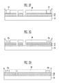
FIG. 1 is a cross-sectional view for explaining a conventional semiconductor device;
FIG. 2A is a cross-sectional view for explaining forming an active layer and protective layer of a method for fabricating a semiconductor device according to an embodiment of the present disclosure;
FIG. 2B is a cross-sectional view for explaining etching the protective layer to have a first aperture of the method for fabricating a semiconductor device according to the embodiment of the present disclosure;
FIGS. 2C and 2D are cross-sectional views for explaining etching the protective layer again to have a second aperture of the method for fabricating a semiconductor device according to the embodiment of the present disclosure;
FIG. 2E is a planar view for explaining etching the protective layer to have the second aperture of the method for fabricating a semiconductor device according to the embodiment of the present disclosure;
FIG. 2F is a cross-sectional view for explaining forming an insulating layer of the method for fabricating a semiconductor device according to the embodiment of the present disclosure;
FIG. 2G is a cross-sectional view between A and A′ for explaining forming a source electrode and drain electrode of the method for fabricating a semiconductor device according to the embodiment of the present disclosure;
FIG. 2H is a cross-sectional view between B and B′ for explaining forming the source electrode and drain electrode of the method for fabricating a semiconductor device according to the embodiment of the present disclosure;
FIG. 2I is a planar view for explaining forming the source electrode and drain electrode of the method for fabricating a semiconductor device according to the embodiment of the present disclosure;
FIG. 2J is a cross-sectional view for explaining forming a photosensitive film of the method for fabricating a semiconductor device according to the embodiment of the present disclosure;
FIG. 2K is a cross-sectional view for explaining forming a driving gate electrode and first additional gate electrode of the method for fabricating a semiconductor device according to the embodiment of the present disclosure;
FIG. 2L is a planar view for explaining the semiconductor device according to the embodiment of the present disclosure;
FIG. 3A is a cross-sectional view for explaining forming an active layer and protective layer of a method for fabricating a semiconductor device according to another embodiment of the present disclosure;
FIG. 3B is a cross-sectional view for explaining forming a source electrode and drain electrode of the method for fabricating a semiconductor device according to the another embodiment of the present disclosure;
FIG. 3C is a cross-sectional view for explaining forming an insulating layer of the method for fabricating a semiconductor device according to the another embodiment of the present disclosure;
FIG. 3D is a cross-sectional view for explaining etching an insulating layer of the method for fabricating a semiconductor device according to the another embodiment of the present disclosure;
FIG. 3E is a planar view for explaining etching the insulating layer of the method for fabricating a semiconductor device according to the another embodiment of the present disclosure;
FIG. 3F is a cross-sectional view for explaining forming a photosensitive film of the method for fabricating a semiconductor device according to the another embodiment of the present disclosure;
FIG. 3G and FIG. 3H are cross-sectional views for explaining etching a protective layer and active layer of the method for fabricating a semiconductor device according to the another embodiment of the present disclosure;
FIG. 3I is a cross-sectional view for explaining forming a driving gate electrode and first additional gate electrode of the method for fabricating a semiconductor device according to the another embodiment of the present disclosure;
FIG. 3J is a planar view for explaining the semiconductor device according to the another embodiment of the present disclosure;
FIG. 4 is a view for explaining a result of simulating a size of an electric field per area of the semiconductor device according to an embodiment of the present disclosure; and
FIG. 5 is a flowchart for explaining the method for fabricating a semiconductor device according to an embodiment of the present disclosure.
DETAILED DESCRIPTION
Hereinafter, embodiments will be described in greater detail with reference to the accompanying drawings. Embodiments are described herein with reference to cross-sectional illustrations that are schematic illustrations of embodiments (and intermediate structures). As such, variations from the shapes of the illustrations as a result, for example, of manufacturing techniques and/or tolerances, are to be expected. Thus, embodiments should not be construed as limited to the particular shapes of regions illustrated herein but may include deviations in shapes that result, for example, from manufacturing. In the drawings, lengths and sizes of layers and regions may be exaggerated for clarity. Like reference numerals in the drawings denote like elements.
Terms such as ‘first’ and ‘second’ may be used to describe various components, but they should not limit the various components. Those terms are only used for the purpose of differentiating a component from other components. For example, a first component may be referred to as a second component, and a second component may be referred to as a first component and so forth without departing from the spirit and scope of the present disclosure. Furthermore, ‘and/or’ may include any one of or a combination of the components mentioned.
Furthermore, a singular form may include a plural from as long as it is not specifically mentioned in a sentence. Furthermore, “include/comprise” or “including/comprising” used in the specification represents that one or more components, steps, operations, and elements exist or are added.
Furthermore, unless defined otherwise, all the terms used in this specification including technical and scientific terms have the same meanings as would be generally understood by those skilled in the related art. The terms defined in generally used dictionaries should be construed as having the same meanings as would be construed in the context of the related art, and unless clearly defined otherwise in this specification, should not be construed as having idealistic or overly formal meanings.
It is also noted that in this specification, “connected/coupled” refers to one component not only directly coupling another component but also indirectly coupling another component through an intermediate component. On the other hand, “directly connected/directly coupled” refers to one component directly coupling another component without an intermediate component.
FIG. 2 (FIGS. 2A to 2L) illustrate a method for fabricating a semiconductor device according to an embodiment of the present disclosure. FIG. 2A illustrates a cross-sectional view for explaining forming an active layer and protective layer of the method for fabricating a semiconductor device according to the embodiment of the present disclosure. Referring to FIG. 2A, an active layer 21 and protective layer 22 are formed on top of a substrate 20. The substrate 20 may be a compound semiconductor substrate or another type of semiconductor substrate, and the materials constituting the substrate 20 may be gallium nitride (GaN), silicon (Si), silicon carbide (SiC), or semi-insulating gallium arsenic (GaAs). It was already aforementioned that in the case of an HEMT device that uses a heterostructure of aluminum gallium nitride (AlGaN) and gallium nitride (GaN), the active layer 21 may include a gallium nitrite buffer layer and aluminum gallium nitride barrier layer, and that the protective layer 22 may include a GaN layer.
FIG. 2B is a cross-sectional view for explaining etching the protective layer to have a first aperture of the method for fabricating a semiconductor device according to the embodiment of the present disclosure, and particularly, a cross-sectional view between A and A′ (see FIG. 2E). Referring to FIG. 2B, the protective layer 22 includes a first aperture h1, and the active layer 21 has a fourth aperture h4 formed in a position corresponding to the first aperture h1. In a subsequent process, a first additional gate electrode 29-1 will be formed in a position corresponding to the first aperture h1 (see FIG. 2K).
FIGS. 2C and 2D are cross-sectional views for explaining etching the protective layer again to have a second aperture of the method for fabricating a semiconductor device according to the embodiment of the present disclosure. FIG. 2C illustrates a cross-sectional view in a case where the active layer 21 corresponding to the first aperture h1 and second aperture h2 areas are all etched. Referring to FIG. 2C, the protective layer 22 includes the first aperture h1 and second aperture h2, and the active layer 21 has a fourth aperture h4 formed in a position corresponding to the first aperture h1 and a fifth aperture h5 formed in a position corresponding to the second aperture h2. In a subsequent process, a driving gate electrode 28 will be formed in a position corresponding to the second aperture h2 (see FIG. 2K). FIG. 2D is a cross-sectional view of a case where the active layer 21 that corresponds to the first aperture h1 and second aperture h2 are partially etched. Either FIG. 2C or FIG. 2D is performed selectively. Referring to FIG. 2D, the protective layer 22 includes the first aperture h1 and second aperture h2, and the active layer 21 includes a first trench s1 formed in a position corresponding to the first aperture h1, and a second trench s2 formed in a position corresponding to the second aperture h2. Depending on the specifications required when fabricating a semiconductor device, it is possible to select whether to etch all the protective layer 22 and active layer 21 that correspond to the positions of the first aperture h1 and second aperture h2 and form the fourth aperture h4 and fifth aperture h5, or to etch the protective layer 22 and active layer 21 partially and form the first trench s1 and second trench s2. In FIGS. 2C and 2D, the second aperture h2 is formed where the driving gate electrode 28 will be formed, but the second aperture h2 may not be needed when fabricating a depleted type mode device. In such a case, there will be no second aperture h2, fifth aperture h5, or second trench s2, and the driving gate electrode 28 may be formed on top of the protective layer 22. In the present embodiment, the second aperture h2 is formed after the first aperture h1 is formed, but this is because since the functions of the first additional gate electrode 29-1 to be formed in a position corresponding to the first aperture h1 and the functions of the driving gate electrode 28 to be formed in a position corresponding to the second aperture h2 are different from each other, the etching specifications (etching method, etching width, and etching depth and so forth) are different as well. If the etching specifications were not so strict, the first aperture h1 and second aperture h2 may be formed at the same time. Referring to FIGS. 2C and 2D, a recess area is formed, and in a subsequent process, the driving gate electrode 28 and first additional gate electrode 29-1 will be formed (see FIG. 2K). However, explanation on FIGS. 2E to 2L will be made based on the assumption that the fourth aperture h4 and fifth aperture h5 are formed. The process of etching the protective layer 22 and active layer 21 to form a recess area is the most important process in an HEMT or MESFET (MEtal Semiconductor Field Effect Transistor) device, and this process is generally conducted while measuring a current in a single step or in numerous steps of a wet or dry etching or in a combination of the dry and wet etching. A wet etching may be performed using an etching solution where phosphoric acid (H3PO4), hydrogen peroxide (H2O2) and water (H2O) are mixed therein, and a dry etching may be performed using gas such as CF4, boron trichloride (BCl3), Cl2 and SF6.
FIG. 2E is a planar view for explaining etching the protection layer to have a second aperture of the method for fabricating a semiconductor device according to the embodiment of the present disclosure. It can be seen that the active layer (not illustrated) and the protective layer 22 are formed on top of the substrate 20, and the first aperture h1, second aperture h2 and third aperture h3 are formed. In a case where the semiconductor device is completed through a subsequent process, the first additional gate electrode 29-1, driving gate electrode 28, and second additional gate electrode 29-2 are each formed in a position corresponding to the first aperture h1, second aperture h2 and third aperture h3, respectively (see FIG. 2L). Herein, an electrical effect caused by each voltage applied to the source electrode 27 a, drain electrode 27 b and driving gate electrode 28 only takes effect within a certain area (see FIG. 2L). This certain area is called an active area, and in this specification, the area where the active layer (not illustrated) and protective layer 22 are formed will be referred to as the active area, for convenience of explanation. In FIG. 2E, an electron or hole flows in a direction illustrated in FIG. 2E, and herein, one of the areas where a strongest electric field is applied are two corner e1, e2 portions that are near the boundaries of the active area. Therefore, the first aperture h1 and third aperture h3, that are recess areas, are formed where an electron or hole may flow from the two corners e1, e2. That is, the first aperture h1 and third aperture h3 are formed on top of the boundaries of the active area. In a subsequent process, the first additional gate electrode 29-1 and second additional gate electrode 29-2 are formed each on top of the second aperture h2 and third aperture h3, respectively, so as to attenuate an intensity of an electric field being applied to the two corners e1, e2 of the driving gate electrode 28 (see FIG. 2K). The cross-sectional view illustrating between A and A′ shows the first aperture h1 whereas the cross-sectional view illustrating between B and B′ does not show the first aperture h1.
FIG. 2F is a cross-sectional view for explaining forming an insulating layer of the method for fabricating a semiconductor device according to the embodiment of the present disclosure. The insulating layer 26 is formed on top of the protecting layer 22, first aperture h1 and second aperture h2, and at least one material selected from alumina (Al2O3), silicon nitride, silicon oxide, BenzoCycloButene (BCB), and porous silicon thin film may constitute the insulating layer 26. The insulating layer 26 may be formed by a method of depositing different materials for a plurality of times. For example, the insulating layer 26 may be formed by depositing an alumina film, and then depositing silicon nitride or silicon oxide on top of the alumina film. The insulating layer 26 has a sixth aperture h6 and seventh aperture h7. The sixth aperture h6 and seventh aperture h7 may be formed by selectively etching only a desired portion after forming the insulating layer 26. The insulating layer 26 may be etched by a dry etching method or wet etching method. Dry etching methods that can be used herein include RIE (Reactive Ion Etching), MERIE (Magnetically Enhanced Reactive Ion Etching) and ICP (Inductive coupled plasma).
FIG. 2G is a cross-sectional view between A and A′ for explaining forming a source electrode and drain electrode of the method for fabricating a semiconductor device according to the embodiment of the present disclosure. The source electrode 27 a and drain electrode 27 b will be formed on top of the sixth aperture h6 and seventh aperture h7 and be electrically connected to the protective layer 22 (see FIG. 2G). At least one material selected from titanium (Ti), aluminum (Al), nickel (Ni), gold (Au), germanium (Ge) and platinum (Pt) may constitute the source electrode 27 a and drain electrode 27 b. For example, in a process for fabricating an HEMT (High Electron Mobility Transistor) device that uses a gallium nitride (GaN) compound semiconductor, the source electrode 27 a and drain electrode 27 b may be formed by depositing Ti, Al, Ni, and Au successively. In a process for fabricating an HEMT or MESFET device that uses gallium arsenide (GaAs) compound semiconductor, the source electrode 27 a and drain electrode 27 b may be formed by depositing AuGe, Ni, and Au successively. After being deposited, the source electrode 27 a and drain electrode 27 b may receive rapid thermal annealing (RTA). In a case where an area corresponding to the position of the first aperture h1 is etched together, the first additional gate electrode 29-1 to be formed subsequently may contact the active layer 21.
FIG. 2H is a cross-sectional view between B and B′ for explaining forming the source electrode and drain electrode of the method for fabricating a semiconductor device according to the embodiment of the present disclosure. Herein, other parts are the same as in FIG. 2G, except that the first aperture h1 is not shown since it is a view of a different cross-section.
FIG. 2I is a planar view for explaining forming the source electrode and drain electrode of the method for fabricating a semiconductor device according to the embodiment of the present disclosure. The protective layer 22, first aperture h1 and second aperture h2 should not be shown since there is the insulating layer 26 on top of them, but they are shown in dotted lines for convenience of explanation and comparison with FIG. 2E. After the insulating layer 26 is formed, it is partially etched, and the source electrode 27 a and drain electrode 27 b are formed on top of the etched portion.
FIG. 2J is a cross-sectional view for explaining forming a photosensitive film of the method for fabricating a semiconductor device according to the embodiment of the present disclosure. A photosensitive film 25 a is formed and patterned on top of the insulating layer 26, source electrode 27 a and drain electrode 27 b.
FIG. 2K is a cross-sectional view for explaining forming a driving gate electrode and first additional gate electrode of the method for fabricating a semiconductor device according to the embodiment of the present disclosure. Referring to FIG. 2K, the driving gate electrode 28 and first additional gate electrode 29-1 are formed through a lift-off process. The lift-off process is a method for forming a metal layer on a portion of a substrate by forming and patterning a photosensitive film, depositing metal, and then removing the photosensitive film. After the photosensitive film 25 a is formed and patterned (see 2J), the metal layer is deposited, and then the photosensitive film 25 a is removed, and thus the driving gate electrode 28 and first additional gate electrode 29-1 are formed on a portion of the substrate. When depositing metal in the lift-off process, a plurality of different kinds of metal may be deposited successively. For example, in a case of fabricating an HEMT device that uses a GaN compound semiconductor, Ni and Au may be deposited successively, and in a case of fabricating an HEMT or MESFET (MEtal Semiconductor Field Effect Transistor) device that uses a GaAs compound semiconductor, Ti, Pt and Au may be deposited successively. When removing the photosensitive film after depositing the metal, the metal deposited on top of the photosensitive film 25 a is removed together with the photosensitive film, and the metal deposited on top of the insulating layer 26 by the patterning remains on top of the insulating layer 26 even after the photosensitive film 25 a is removed. The first additional gate electrode 29-1 includes a first additional gate electrode lower part 29-1 a having a first area and a first additional gate electrode upper part 29-1 b having a second area that is bigger than the first area. Furthermore, the driving gate electrode 28 includes a driving gate electrode lower part 28 a, and a driving gate electrode upper part 28 b that has a bigger area than the area of the driving gate electrode lower part 28 a. Forming such a T-shaped gate electrode improves velocity characteristics and noise characteristics, and reduces a gate width without increasing a resistance of the gate electrode. Although not illustrated in FIG. 2K, in a case where a second additional gate electrode 29-2 is formed, in the same manner as the first additional gate electrode 29-1, the second additional gate electrode 29-2 includes a second additional gate electrode lower part 29-2 a having a third area and a second additional gate electrode upper part 29-2 b having a fourth area that is bigger than the third area.
FIG. 2L is a planar view for explaining the semiconductor device according to the embodiment of the present disclosure. Although the protective layer 22, driving gate electrode lower part 28 a, first additional gate electrode 29-1, and second additional gate electrode 29-2 are not shown in the planar view, they are shown in dotted lines in the planar view for convenience of explanation. It can be seen that the driving gate electrode 28, first additional gate electrode 29-1, and second additional gate electrode 29-2 are formed after the step of forming the source electrode and drain electrode illustrated in FIG. 2I. Furthermore, after the step of forming the gate electrode and additional gate electrode illustrated in FIG. 2J, a connecting electrode 29-3 is formed on top of the first additional gate electrode 29-1 and second additional gate electrode 29-2. The connecting electrode 29-3 electrically connects the first additional gate electrode 29-1 and second additional gate electrode 29-2, and the connecting electrode 29-3 may be formed directly on top of the insulating layer 26, or may be formed in an air-bridge format so that it does not touch the insulating layer 26. The first additional gate electrode 29-1 and second additional gate electrode 29-2 may be electrically connected to the driving gate electrode 28 and source electrode 27 a, or may be electrically floated. Referring to FIGS. 2A to 2L, a semiconductor device was explained that has the insulating layer 26 between the driving gate electrode 28 and substrate 20, or between the driving gate electrode 28 and active layer 21. Such a structure may be related to a power device.
FIG. 3 (FIGS. 3A to 3J) illustrate a method for fabricating a semiconductor device according to another embodiment of the present disclosure. FIG. 3A is a cross-sectional view for explaining forming an active layer and protective layer of the method for fabricating a semiconductor device according to the another embodiment of the present disclosure. Since this embodiment is not so much different from that of FIG. 2A, detailed explanation may be omitted. An active layer 31 is formed on top of a substrate 30, and a protective layer 32 is formed on top of the active layer 31. The materials constituting the active layer 31 and protective layer 32 are very similar to the materials constituting the active layer 21 and protective layer 22, and thus detailed explanation may be omitted.
FIG. 3B is a cross-sectional view for explaining forming a source electrode and drain electrode of the method for fabricating a semiconductor device according to the another embodiment of the present disclosure. The source electrode 33 a and drain electrode 33 b are formed on top of the protective layer 32. The materials that constitute the source electrode 33 a and drain electrode 33 b are very similar to the materials constituting the source electrode 27 a and drain electrode 27 b, and thus detailed explanation may be omitted.
FIG. 3C is a cross-sectional view for explaining forming an insulating layer of the method for fabricating a semiconductor device according to the another embodiment of the present disclosure. The insulating layer 34 is formed on top of the protective layer 32, source electrode 33 a and drain electrode 33 b. The materials that constitute the insulating layer 34 and the forming method thereof are very similar to those of the insulating layer 26, and thus detailed explanation may be omitted.
FIG. 3D is a cross-sectional view for explaining etching the insulating layer of the method for fabricating a semiconductor device according to the another embodiment of the present disclosure. The insulating layer 34 is etched to form a sixth aperture h16 and seventh aperture h17. A first aperture h11 and second aperture h12 will each be formed in a position corresponding to the sixth aperture h16 and seventh aperture h17 (see FIG. 3G and FIG. 3H). That is, a patterned insulating layer 34 may be used as a mask for etching the protective layer 32 or active layer 31. Furthermore, a first additional gate electrode 38-1 and driving gate electrode 37 will each be formed in a position corresponding to the sixth aperture h16 and seventh aperture h17 (see FIG. 3I).
FIG. 3E is a planar view for explaining etching the insulating layer of the method for fabricating a semiconductor device according to the another embodiment of the present disclosure. For convenience of explanation, the protective layer 32, source electrode 33 a, and drain electrode 33 b covered by the insulating layer 34 are shown in dotted lines. It can be seen that the active layer (not illustrated) and protective layer 32 are formed on top of the substrate 30, and the sixth aperture h16, seventh aperture h7 and eighth aperture h18 are formed. Herein, for convenience of explanation, the area where the active layer (not illustrated) and protective layer 32 are formed is referred to as an active area. In a case where the semiconductor device is completed through a subsequent process, the first additional gate electrode 38-1, driving gate electrode 37 and second additional gate electrode 38-2 are each formed in a position corresponding to the sixth aperture h16, seventh aperture h17, and eighth aperture h18, respectively (see FIG. 3J). In FIG. 3E, an electron or hole flows in a direction illustrated in FIG. 3E, and herein, one of the areas where a strongest electric field is applied are two corner e11, e12 portions that are near the boundaries of the active area. Therefore, the sixth aperture h16 and eighth aperture h18, that are recess areas, are formed where an electron or hole may flow from the two corners e11, e12. That is, the sixth aperture h16 and eighth aperture h18 are formed on top of the boundaries of the active area. In a subsequent process, the first additional gate electrode 38-1 and second additional gate electrode 38-2 are formed each on top of the sixth aperture h16 and eighth aperture h18, respectively, so as to attenuate an intensity of an electric field being applied to the two corners e11, e12 of the driving gate electrode 37 (see FIG. 3J). The method of etching the insulating layer 34 is very similar to the method of etching the insulating layer 26, and thus detailed explanation is omitted.
FIG. 3F is a cross-sectional view for explaining forming a photosensitive film of the method for fabricating a semiconductor device according to the another embodiment of the present disclosure. On top of the insulating layer 34, a first photosensitive film 35 a, second photosensitive film 35 b, and third photosensitive film 35 c may be formed successively, and the first photosensitive film 35 a, second photosensitive film 35 b, and third photosensitive film 35 c may all be referred to collectively as a photosensitive film 35. The first photosensitive film 35 a, second photosensitive film 35 b, and third photosensitive film 35 c may be configured by a combination of polymethyl metacrylate (PMMA)/copolymer/polymethyl metacrylate (PMMA), ZEP/PMGI/ZEP etc. When forming the photosensitive film 35, the photosensitive film 35 may be patterned using the electron-beam lithography process, and the second photosensitive film 35 b may be formed after the forming and patterning of the first photosensitive film 35 a. Furthermore, in FIG. 3F, the photosensitive film 35 is formed to have three layers, but the photosensitive film 35 may be formed to have one or two layers instead.
FIGS. 3G and 3H are cross-sectional views for explaining etching the protective layer and active layer of the method for fabricating a semiconductor device according to another embodiment of the present disclosure. In FIG. 3G, the protective layer 32 in a position corresponding to the sixth aperture h16 and seventh aperture h17 are all etched to form the first aperture h11 and second aperture h12, and the active layer 31 is partially etched to form the first shallow, or trench, s11 and second trench s12. Referring to FIG. 3H, the protective layer 32 in a position corresponding to the sixth aperture h16 and seventh aperture h17 are all etched to form the first aperture h11 and second aperture h12, and the active layer 31 is also all etched to form the fourth aperture h14 and fifth aperture h15. The process of etching the active layer 31 and protective layer 32 to form a recess area is very similar to the process of etching the active layer 21 and protective layer 22 and forming a recess area, and thus detailed explanation may be omitted. Depending on the specifications required when fabricating a semiconductor device, it is possible to select whether to etch all the active layer 31 that corresponds to the positions of the first aperture h11 and second aperture h12 and form the fourth aperture h14 and fifth aperture h15, or to etch the active layer 31 partially and form the first trench s11 and second trench s12. However, explanation on FIGS. 3I to 3J will be made based on an assumption that the first trench s11 and second trench s12 are formed as in FIG. 3G. Furthermore, as aforementioned, the second aperture h12 may not be needed when fabricating a depleted type mode device. In such a case, there will be no second aperture h12, fifth aperture h15, or second trench s12, and the driving gate electrode 37 may be formed on top of the protective layer 32. FIG. 3I is a cross-sectional view for explaining forming the driving gate electrode and first additional gate electrode of the method for fabricating a semiconductor device according to the another embodiment of the present disclosure. Referring to FIG. 3I, the driving gate electrode 37 and first additional gate electrode 38-1 are formed through the lift-off process. Explanation on the lift-off process, materials constituting the driving gate electrode 37 and the first additional gate electrode 38-1 were already made referring to FIG. 2K, and thus detailed explanation may be omitted. The first additional gate electrode 38-1 includes a first additional gate electrode lower part 38-1 a having a first area and a first additional gate electrode upper part 38-1 b having a second area that is bigger than the first area. Furthermore, the driving gate electrode 37 includes a driving gate electrode lower part 37 a and a driving gate electrode upper part 37 b having a area bigger than the area of the driving gate electrode lower part 37 a. Furthermore, the second area that is the area of the first additional gate electrode upper part 38-1 b may be, for example, defined as a minimum area of the first additional gate electrode upper part 38-1 b, or defined as an average area of the first additional gate electrode upper part 38-1 b. Although not illustrated in FIG. 3I, when the second additional gate electrode 38-2 is formed, just as the first additional gate electrode 38-1, the second additional gate electrode 38-2 includes a second additional gate electrode lower part 38-2 a having a third area and a second additional gate electrode upper part 38-2 b having a fourth area that is bigger than the third area. The advantages of such a gate electrode, materials that constitute the driving gate electrode 37, and materials constituting the first additional gate electrode 38-1 were already explained with reference to FIG. 2K.
FIG. 3J is a planar view for explaining the semiconductor device according to the another embodiment of the present disclosure. For convenience of explanation, the source electrode 33 a, drain electrode 33 b, driving gate electrode lower part 37 a, first additional gate electrode 38-1, and second additional gate electrode 38-2 are shown in dotted lines. In can be seen that after the etching the insulating layer illustrated in FIG. 3E, the driving gate electrode 37, first additional gate electrode 38-1, and second additional gate electrode 38-2 are formed. Furthermore, after the etching the gate electrode and additional gate electrode illustrated in FIG. 3I, a connecting electrode 38-3 is formed on top of the first additional gate electrode 38-1 and second additional gate electrode 38-2. The first additional gate electrode 38-1 and second additional gate electrode 38-2 may be electrically connected to the driving gate electrode 37 or source electrode 33 a, or may be electrically floated. In FIGS. 3A to 3J, a semiconductor device was explained wherein the driving gate electrode 37 contacts the active layer 31 or substrate 30 and forms a schottky contact. Such a structure may be related to an RF (RadioFrequency) device.
FIG. 4 is a view for explaining a result of simulating a size of an electric field per area of the semiconductor device according to an embodiment of the present disclosure. FIG. 4 shows the result of simulating changes in a size of an electric field as a function of a flowing direction of a current or hole with reference to a source electrode (S) regarding the semiconductor device of FIG. 2L or FIG. 3J. In FIG. 4, it can be seen that changes in a size of an electric field as a function of each recess area (between A and A′) and non-recess area (between B and B′) are simulated. The non-recess area having the strongest electric field is a gate edge in a drain direction, that is, the area in the gate closest from a drain electrode (D), an electric field value at the gate edge being 3.5×10⁶ V/cm. On the other hand, as for the recess area, an electric field value at the gate edge in the drain direction is reduced to 5×10⁵ V/cm. That is, it can be seen that due to the first additional gate electrode 29-1, 38-1, Fgate and second additional gate electrode 29-2, 38-2 formed in the recess area, the maximum value of the electric field being applied to the semiconductor device is reduced.
FIG. 5 is a flowchart for explaining the method for fabricating a semiconductor device according to an embodiment of the present disclosure. Hereinafter, explanation will be made with reference to FIGS. 2A to 2L and FIG. 5.
At the step of forming the active layer on top of the substrate (S100), the active layer 21 is formed on top of the substrate 20. The materials constituting the substrate 20 and active layer 21 were already explained by way of an example.
At the step of forming the protective layer on top of the active layer (S200), the protective layer 22 is formed on top of the active layer 21. The materials constituting the protective layer 22 were already explained by way of an example.
At the step of forming the first aperture and second aperture (S300), the step of etching (S310) and the step of etching again (S320) are performed. At the step of etching (S310), the protective layer 22 is etched to have the first aperture h1. The active layer 21 corresponding to the first aperture h1 may be etched entirely or partially, and in a subsequent process, the first additional gate electrode 29-1 may be formed in a position corresponding to the first aperture h1. At the step of etching (S310), the third aperture h3 may be formed at the same the first aperture h1 is formed. The second additional gate electrode 29-2 may be formed subsequently in a position corresponding to the third aperture h3.
At the step of etching again (S320), the protective layer 22 is etched to have the second aperture h2. The active layer 21 in a position corresponding to the second aperture h2 may be etched entirely or partially, and in a subsequent process, the driving gate electrode 28 may be formed in a position corresponding to the second aperture h2. In FIG. 5, the first aperture h1 is etched first, but the second aperture h2 may be formed first. Since the first aperture and second aperture are formed in a separate etching process, even if the etching specifications (etching width, etching depth etc.) for forming the first aperture h1 are different from the etching specifications for forming the second aperture h2, the first aperture h1 and second aperture h2 may be formed while satisfying the two etching specifications. When fabricating a depleted type mode device, the second aperture h2 may not be needed. In such a case, the step of etching again (S320) may be omitted.
At the step of forming the insulating layer (S400), after the insulating layer 26 is formed, the insulating layer 26 is selectively etched to form the sixth aperture h6 and seventh aperture h7. When the insulating layer 26 corresponding to the first aperture h1 is etched selectively, the first additional gate electrode 29-1 to be formed subsequently may contact the active layer 21 or substrate 20.
At the step of forming the source electrode and drain electrode (S500), the source electrode 27 a and drain electrode 27 b are each formed on top of the sixth aperture h6 and seventh aperture h7, respectively. The source electrode 27 a and drain electrode 27 b are electrically connected to the protective layer 22.
The step of forming the driving gate electrode and first additional gate electrode (S600) is a lift-off process, wherein the step of forming the photosensitive film (S610), the step of forming the metal layer (S620), and the step of removing the photosensitive film (S630) are performed. At the step of forming the photosensitive film (S610), the photosensitive film 25 a is formed and patterned. At the step of forming the metal layer (S620), the metal layer is deposited. At the step of removing the photosensitive film (S630), the photosensitive film 25 a is removed, the metal layer deposited on top of the photosensitive film 25 a is removed together, and only the metal layer deposited on top of the insulating layer 26 due to the patterning is maintained. The first additional gate electrode 29-1 of the metal layer is formed in a position corresponding to the first aperture h1. Additionally, the driving gate electrode 28 of the metal layer is formed in a position corresponding to the second aperture h2, and the second additional gate electrode 29-2 of the metal layer may be formed in a position corresponding to the third aperture h3.
At the step of forming the connecting electrode (S700), the connecting electrode 29-3 that electrically connects the first additional gate electrode 29-1 and second additional gate electrode 29-2 is formed.
Example embodiments have been disclosed herein, and although specific terms are employed, they are used and are to be interpreted in a generic and descriptive sense only and not for purpose of limitation. In some instances, as would be apparent to one of ordinary skill in the art as of the filing of the present application, features, characteristics, and/or elements described in connection with a particular embodiment may be used singly or in combination with features, characteristics, and/or elements described in connection with other embodiments unless otherwise specifically indicated. Accordingly, it will be understood by those of skill in the art that various changes in form and details may be made without departing from the spirit and scope of the present invention as set forth in the following claims.

Claims (14)

What is claimed is:
1. A semiconductor device comprising:
a substrate;
an active layer formed on the substrate, the active layer extending in a first direction;
a protective layer formed on the active layer and having a first aperture exposing a portion of the active layer in a second direction crossing the first direction;
a source electrode formed on one side of the protective layer;
a drain electrode formed on the other side of the protective layer;
a driving gate electrode formed between the source electrode and the drain electrode in the first aperture, wherein the protective layer has second and third apertures adjacent to opposite ends of the driving gate electrode, the second and third apertures exposing opposite edges of the active layer in the second direction; and
first and second gate width controlling electrodes formed in the second and third apertures on opposite edges of the active layer in the second direction between the driving gate electrode and the drain electrode in the first direction to control a channel width of the active layer in the second direction.
2. The semiconductor device according to claim 1,
wherein the first and second gate width controlling electrodes are formed on top of a boundary, as viewed in the top plan view, of an active area affected by a voltage applied to each of the source electrode, the drain electrode, and the driving gate electrode.
3. The semiconductor device according to claim 1,
wherein the active layer has a first trench with a thickness that is thinner than that of the active layer where the first trench is not formed, and formed in a position corresponding to the first aperture.
4. The semiconductor device according to claim 3, further comprising an insulating layer formed between the active layer and the first gate width controlling electrode,
wherein the first aperture is separated from the second aperture by a cross-section of the insulating layer.
5. The semiconductor device according to claim 3, wherein the first gate width controlling electrode is located at least partially within the first trench.
6. The semiconductor device according to claim 1, wherein the semiconductor device further comprises an insulating layer formed between the substrate and the first gate width controlling electrode.
7. The semiconductor device according to claim 1, wherein the active layer comprises a buffer layer formed on top of the substrate, and a barrier layer formed on top of the buffer layer,
a material constituting the buffer layer comprises GaN,
a material constituting the barrier layer comprises AlGaN, and
a material constituting the protective layer comprises GaN.
8. The semiconductor device according to claim 1, wherein the source electrode, drain electrode, driving gate electrode, and first gate width controlling electrode are made of at least one selected from Ti, Al, Ni, Au, Ge, and Pt.
9. The semiconductor device according to claim 1, wherein the first gate width controlling electrode comprises a first additional gate electrode lower part having a first width and a first additional gate electrode upper part having a second width that is larger than the first width,
the second gate width controlling electrode comprises a second additional gate electrode lower part having a third width and a second additional gate electrode upper part having a fourth width that is larger than the third width, and
the semiconductor device further comprises a connecting electrode formed on top of the first gate width controlling electrode and second gate width controlling electrode, and configured to electrically connect the first gate width controlling electrode and second gate width controlling electrode.
10. The semiconductor device according to claim 1, further comprising:
an insulating layer on the protective layer,
wherein the active layer includes a first trench at a location corresponding to the first aperture,
wherein a width of the first trench in the active layer is greater than a width of an opening in the insulating layer, and
wherein the first gate width controlling electrode extends through the opening in the insulating layer into the trench in the active layer to contact one of the active layer and the substrate.
11. The semiconductor device according to claim 1, wherein the second aperture includes a trench extending in a line in a width direction,
the first aperture is spaced apart from the second aperture in a length direction perpendicular to the width direction, such that the first aperture is separated from the second aperture by the cross-section of the active layer and the protective layer in the length direction.
12. The semiconductor device according to claim 1, wherein the second aperture includes a trench extending in a line in a width direction,
the first and third apertures are spaced apart from the second aperture in a length direction perpendicular to the width direction, and
the third aperture is spaced apart from the first aperture in the width direction.
13. The semiconductor device according to claim 1, further comprising a connecting electrode extending in the first direction to electrically connect the first gate width controlling electrode to the second gate width controlling electrode.
14. The semiconductor device according to claim 13, further comprising an insulating layer formed between the substrate and the first gate width controlling electrode, between the substrate and the second gate width controlling electrode, and on the protective layer,
wherein the connecting electrode extends between the first gate width controlling electrode and the second gate width controlling electrode on the insulating layer.
US14/658,121 2014-06-26 2015-03-13 Semiconductor device and fabrication method thereof Active US9899226B2 (en)

Applications Claiming Priority (2)

Application Number Priority Date Filing Date Title
KR10-2014-0078693 2014-06-26
KR1020140078693A KR102135163B1 (en) 2014-06-26 2014-06-26 Semiconductor device and fabrication method thereof

Publications (2)

Publication Number Publication Date
US20150380482A1 US20150380482A1 (en) 2015-12-31
US9899226B2 true US9899226B2 (en) 2018-02-20

Family

ID=54931398

Family Applications (1)

Application Number Title Priority Date Filing Date
US14/658,121 Active US9899226B2 (en) 2014-06-26 2015-03-13 Semiconductor device and fabrication method thereof

Country Status (2)

Country Link
US (1) US9899226B2 (en)
KR (1) KR102135163B1 (en)

Cited By (1)

* Cited by examiner, † Cited by third party
Publication number Priority date Publication date Assignee Title
US20170148906A1 (en) * 2015-11-24 2017-05-25 Stmicroelectronics S.R.L. Normally-off transistor with reduced on-state resistance and manufacturing method

Families Citing this family (1)

* Cited by examiner, † Cited by third party
Publication number Priority date Publication date Assignee Title
CN109103245A (en) * 2018-07-26 2018-12-28 厦门市三安集成电路有限公司 A kind of double-T shaped grid and production method and application

Citations (11)

* Cited by examiner, † Cited by third party
Publication number Priority date Publication date Assignee Title
KR100276077B1 (en) 1998-05-11 2001-01-15 이계철 Fabrication method of fine T-shaped gate electrode
US7141464B2 (en) 2004-10-12 2006-11-28 Electronics And Telecommunications Research Institute Method of fabricating T-type gate
WO2007014036A2 (en) 2005-07-21 2007-02-01 Cree, Inc. Switch mode power amplifier using fet with field plate extension
KR100782430B1 (en) 2006-09-22 2007-12-05 한국과학기술원 Gallium Nitride based high electron mobility transistor structure with internal field electrodes for high power
KR20080101378A (en) 2007-05-17 2008-11-21 주식회사 동부하이텍 Manufacturing Method of Flash Memory Device
US7573078B2 (en) 2004-05-11 2009-08-11 Cree, Inc. Wide bandgap transistors with multiple field plates
US20130069127A1 (en) 2011-09-21 2013-03-21 Electronics And Telecommunications Research Institute Field effect transistor and fabrication method thereof
US20140001531A1 (en) 2012-06-28 2014-01-02 Taiwan Semiconductor Manufacturing Co., Ltd. Damascene non-volatile memory cells and methods for forming the same
US20140151747A1 (en) * 2012-11-30 2014-06-05 Samsung Electronics Co., Ltd. High electron mobility transistor including plurality of gate electrodes
US20150060948A1 (en) * 2013-09-02 2015-03-05 Renesas Electronics Corporation Semiconductor device
US20150255547A1 (en) * 2012-03-29 2015-09-10 Agency For Science, Technology And Research III-Nitride High Electron Mobility Transistor Structures and Methods for Fabrication of Same

Family Cites Families (3)

* Cited by examiner, † Cited by third party
Publication number Priority date Publication date Assignee Title
JP5548909B2 (en) * 2010-04-23 2014-07-16 古河電気工業株式会社 Nitride semiconductor device
JP5866773B2 (en) * 2011-02-25 2016-02-17 富士通株式会社 Compound semiconductor device and manufacturing method thereof
JP5874173B2 (en) * 2011-02-25 2016-03-02 富士通株式会社 Compound semiconductor device and manufacturing method thereof

Patent Citations (13)

* Cited by examiner, † Cited by third party
Publication number Priority date Publication date Assignee Title
KR100276077B1 (en) 1998-05-11 2001-01-15 이계철 Fabrication method of fine T-shaped gate electrode
US7573078B2 (en) 2004-05-11 2009-08-11 Cree, Inc. Wide bandgap transistors with multiple field plates
US7141464B2 (en) 2004-10-12 2006-11-28 Electronics And Telecommunications Research Institute Method of fabricating T-type gate
WO2007014036A2 (en) 2005-07-21 2007-02-01 Cree, Inc. Switch mode power amplifier using fet with field plate extension
KR20080036002A (en) 2005-07-21 2008-04-24 크리 인코포레이티드 Switchmode Power Amplifier with FET with Field Plate Extension
KR100782430B1 (en) 2006-09-22 2007-12-05 한국과학기술원 Gallium Nitride based high electron mobility transistor structure with internal field electrodes for high power
US7696535B2 (en) 2006-09-22 2010-04-13 Korea Advanced Institute Of Science And Technology Gallium nitride high electron mobility transistor having inner field-plate for high power applications
KR20080101378A (en) 2007-05-17 2008-11-21 주식회사 동부하이텍 Manufacturing Method of Flash Memory Device
US20130069127A1 (en) 2011-09-21 2013-03-21 Electronics And Telecommunications Research Institute Field effect transistor and fabrication method thereof
US20150255547A1 (en) * 2012-03-29 2015-09-10 Agency For Science, Technology And Research III-Nitride High Electron Mobility Transistor Structures and Methods for Fabrication of Same
US20140001531A1 (en) 2012-06-28 2014-01-02 Taiwan Semiconductor Manufacturing Co., Ltd. Damascene non-volatile memory cells and methods for forming the same
US20140151747A1 (en) * 2012-11-30 2014-06-05 Samsung Electronics Co., Ltd. High electron mobility transistor including plurality of gate electrodes
US20150060948A1 (en) * 2013-09-02 2015-03-05 Renesas Electronics Corporation Semiconductor device

Non-Patent Citations (4)

* Cited by examiner, † Cited by third party
Title
A. Chini et al., "Power and Linearity Characteristics of Field-Plated Recessed-Gate AlGaN-GaN HEMTs", IEEE Electron Device Letters, vol. 25, No. 5, pp. 229-231, May 2004.
Eizo Mitani et al., "Mass-Production of High-Voltage GaAs and GaN Devices", CS MANTECH Conference, pp. 183-186, Apr. 24-27, 2006.
Eldad Bahat-Treidel et al., "AlGaN/GaN/AlGaN DH-HEMTs Breakdown Voltage Enhancement Using Multiple Grating Field Plates (MGFPs)", IEEE Transactions on Electron Devices, vol. 57, No. 6, pp. 1208-1216, Jun. 2010.
Ho-Kyun Ahn et al., "Normally-off dual gate AlGaN/GaN MISFET with selective area-recessed floating gate", Solid-State Electronics, vol. 95, pp. 42-45, May 2014.

Cited By (3)

* Cited by examiner, † Cited by third party
Publication number Priority date Publication date Assignee Title
US20170148906A1 (en) * 2015-11-24 2017-05-25 Stmicroelectronics S.R.L. Normally-off transistor with reduced on-state resistance and manufacturing method
US11222969B2 (en) 2015-11-24 2022-01-11 Stmicroelectronics S.R.L. Normally-off transistor with reduced on-state resistance and manufacturing method
US12457765B2 (en) 2015-11-24 2025-10-28 Stmicroelectronics S.R.L. Normally-off transistor with reduced on-state resistance and manufacturing method

Also Published As

Publication number Publication date
US20150380482A1 (en) 2015-12-31
KR20160001744A (en) 2016-01-07
KR102135163B1 (en) 2020-07-20

Similar Documents

Publication Publication Date Title
EP1843390B1 (en) Semiconductor device provided with mis structure and method for manufacturing the same
US9577064B2 (en) High electron mobility transistors with field plate electrode
JP4913046B2 (en) Method of forming a III-V substrate structure having an enhancement mode transistor device and a depletion mode transistor device
CN110233104B (en) High electron mobility transistor with double-thickness barrier layer
CN105453216A (en) Gates with self-aligned bumps for enhancement mode gallium nitride transistors
US11538908B2 (en) Semiconductor device
JP7690029B2 (en) Field effect transistor having at least partially buried field plate
US9899226B2 (en) Semiconductor device and fabrication method thereof
KR101243836B1 (en) Semiconductor devices and methods forming thereof
TWI521641B (en) Method of fabricating a gallium nitride device and a self-aligned isolation portion in an integrated circuit
US12369380B2 (en) Transistor with dielectric spacers and field plate and method of fabrication therefor
US12266713B2 (en) Transistor with dielectric spacers and method of fabrication therefor
US8952422B2 (en) Transistor and method of fabricating the same
CN109727918B (en) Structure of integrated enhancement mode and depletion mode field effect transistor and manufacturing method thereof
US20080064155A1 (en) Method for Producing a Multi-Stage Recess in a Layer Structure and a Field Effect Transistor with a Multi-Recessed Gate
US12477803B2 (en) Transistor with defect mitigation structures
US20250142924A1 (en) Semiconductor device with multi-step gate and recessed multi-step field plate with field plate spacers and method of fabrication
US20250142923A1 (en) Semiconductor device with multi-step gate and recessed multi-step field plate and method of fabrication therefor
KR20190042424A (en) Manufacturing method of microwave device
CN120201743A (en) Semiconductor device and preparation method thereof
JP2005209876A (en) Semiconductor device and method for manufacturing the same
JP2007149885A (en) Compound semiconductor switch circuit device and manufacturing method thereof
JP2018082048A (en) Compound semiconductor device and manufacturing method thereof

Legal Events

Date Code Title Description
AS Assignment

Owner name: ELECTRONICS AND TELECOMMUNICATIONS RESEARCH INSTIT

Free format text: ASSIGNMENT OF ASSIGNORS INTEREST;ASSIGNORS:AHN, HO KYUN;KIM, HAE CHEON;LIM, JONG WON;AND OTHERS;SIGNING DATES FROM 20150306 TO 20150309;REEL/FRAME:035167/0456

STCF Information on status: patent grant

Free format text: PATENTED CASE

MAFP Maintenance fee payment

Free format text: PAYMENT OF MAINTENANCE FEE, 4TH YR, SMALL ENTITY (ORIGINAL EVENT CODE: M2551); ENTITY STATUS OF PATENT OWNER: SMALL ENTITY

Year of fee payment: 4

FEPP Fee payment procedure

Free format text: MAINTENANCE FEE REMINDER MAILED (ORIGINAL EVENT CODE: REM.); ENTITY STATUS OF PATENT OWNER: SMALL ENTITY