US9897490B2 - Temperature measurement device, integrated circuit, and temperature measurement method - Google Patents
Temperature measurement device, integrated circuit, and temperature measurement method Download PDFInfo
- Publication number
- US9897490B2 US9897490B2 US14/618,911 US201514618911A US9897490B2 US 9897490 B2 US9897490 B2 US 9897490B2 US 201514618911 A US201514618911 A US 201514618911A US 9897490 B2 US9897490 B2 US 9897490B2
- Authority
- US
- United States
- Prior art keywords
- digital value
- semiconductor element
- current
- voltage
- junction
- Prior art date
- Legal status (The legal status is an assumption and is not a legal conclusion. Google has not performed a legal analysis and makes no representation as to the accuracy of the status listed.)
- Active, expires
Links
Images


Classifications
-
- G—PHYSICS
- G01—MEASURING; TESTING
- G01K—MEASURING TEMPERATURE; MEASURING QUANTITY OF HEAT; THERMALLY-SENSITIVE ELEMENTS NOT OTHERWISE PROVIDED FOR
- G01K7/00—Measuring temperature based on the use of electric or magnetic elements directly sensitive to heat ; Power supply therefor, e.g. using thermoelectric elements
- G01K7/01—Measuring temperature based on the use of electric or magnetic elements directly sensitive to heat ; Power supply therefor, e.g. using thermoelectric elements using semiconducting elements having PN junctions
-
- G—PHYSICS
- G01—MEASURING; TESTING
- G01K—MEASURING TEMPERATURE; MEASURING QUANTITY OF HEAT; THERMALLY-SENSITIVE ELEMENTS NOT OTHERWISE PROVIDED FOR
- G01K7/00—Measuring temperature based on the use of electric or magnetic elements directly sensitive to heat ; Power supply therefor, e.g. using thermoelectric elements
- G01K7/16—Measuring temperature based on the use of electric or magnetic elements directly sensitive to heat ; Power supply therefor, e.g. using thermoelectric elements using resistive elements
-
- H—ELECTRICITY
- H03—ELECTRONIC CIRCUITRY
- H03M—CODING; DECODING; CODE CONVERSION IN GENERAL
- H03M1/00—Analogue/digital conversion; Digital/analogue conversion
- H03M1/12—Analogue/digital converters
- H03M1/34—Analogue value compared with reference values
- H03M1/36—Analogue value compared with reference values simultaneously only, i.e. parallel type
Definitions
- the embodiments discussed herein are related to a temperature measurement device, an integrated circuit, and a temperature measurement method.
- a temperature measurement device that utilizes a characteristic of proportionality between the inter-base-emitter voltage difference of a pair of bipolar transistors supplied with mutually different emitter currents, and the absolute temperature.
- errors in temperature measurement values are caused by a mismatch between the pair of bipolar transistors (relative variation of the characteristics) and the like.
- Dynamic element matching is used as a method of minimizing temperature measurement value errors arising from the mismatch between the pair of bipolar transistors and the like.
- a temperature measurement device includes: a first semiconductor element and a second semiconductor element that include respective pn junctions; a first current output circuit configured to output a first current and a second current of a different magnitude from the first current in accordance with a control voltage supplied to a current control terminal; a first connection switching circuit configured to switch connections of the first semiconductor element and the second semiconductor element with the first current output circuit so as to give either state of a first sensing state in which the first current flows in a forward direction with respect to the pn junction of the first semiconductor element and the second current flows in a forward direction with respect to the pn junction of the second semiconductor element, or a second sensing state in which the first current flows in the forward direction with respect to the pn junction of the second semiconductor element and the second current flows in the forward direction with respect to the pn junction of the first semiconductor element; an AD convertor configured to convert, in the first sensing state, a difference between a forward direction voltage of the pn junction of the first semiconductor element and
- FIG. 1 is a block diagram illustrating a configuration of a temperature measurement device according to an exemplary embodiment of technology disclosed herein.
- FIG. 2 is a block diagram illustrating a detailed configuration of a temperature measurement device according to an exemplary embodiment of technology disclosed herein.
- FIG. 3 is a block diagram illustrating a configuration of a digital operation section according to an exemplary embodiment of technology disclosed herein.
- FIG. 4 is a block diagram illustrating a configuration of a controller according to an exemplary embodiment of technology disclosed herein.
- FIG. 5 is a diagram illustrating an example of a connection configuration of a temperature measurement device according to an exemplary embodiment of technology disclosed herein.
- FIG. 6 is a flowchart illustrating a flow of processing in a measurement control program according to an exemplary embodiment of technology disclosed herein.
- FIG. 7 is a flowchart illustrating processing in a measurement control program according to an exemplary embodiment of technology disclosed herein.
- FIG. 8 is a block diagram illustrating an example of a connection configuration of a temperature measurement device according to an exemplary embodiment of technology disclosed herein.
- FIG. 9 is a block diagram illustrating an example of a connection configuration of a temperature measurement device according to an exemplary embodiment of technology disclosed herein.
- FIG. 10 is a block diagram illustrating an example of a connection configuration of a temperature measurement device according to an exemplary embodiment of technology disclosed herein.
- FIG. 11 is a block diagram illustrating an example of a connection configuration of a temperature measurement device according to an exemplary embodiment of technology disclosed herein.
- FIG. 12 is a block diagram illustrating an example of a connection configuration of a temperature measurement device according to an exemplary embodiment of technology disclosed herein.
- FIG. 13 is a block diagram illustrating an example of a connection configuration of a temperature measurement device according to an exemplary embodiment of technology disclosed herein.
- FIG. 14 is a block diagram illustrating an example of a connection configuration of a temperature measurement device according to an exemplary embodiment of technology disclosed herein.
- FIG. 15 is a block diagram illustrating an example of a connection configuration of a temperature measurement device according to an exemplary embodiment of technology disclosed herein.
- FIG. 16 is a diagram illustrating correspondence relationships between a state of a temperature measurement device, and a voltage measured in an AD convertor and a corresponding digital value according to an exemplary embodiment of technology disclosed herein.
- FIG. 17 is a flowchart illustrating a flow of processing in temperature computation program according to an exemplary embodiment of technology disclosed herein.
- FIG. 18 is a block diagram illustrating an example of a configuration of an integrated circuit 100 provided with a temperature measurement device according to an exemplary embodiment of technology disclosed herein.
- FIG. 19 is a flowchart illustrating a flow of processing in a temperature computation processing program according to an exemplary embodiment of technology disclosed herein.
- FIG. 20 is a flowchart illustrating a flow of processing in a temperature computation processing program according to an exemplary embodiment of technology disclosed herein.
- FIG. 21 is a block diagram illustrating a configuration of a digital computation section according to an exemplary embodiment of technology disclosed herein.
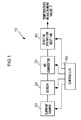
- FIG. 1 is a block diagram illustrating a configuration of a temperature measurement device 10 according to technology disclosed herein.
- the temperature measurement device 10 includes a sensor 20 , an AD converter 30 , a digital operation section 40 , a current source 50 , and a controller 60 .
- the temperature measurement device 10 is an example of a temperature measurement device according to technology disclosed herein.
- the sensor 20 includes a pair of semiconductor elements with pn junctions, and outputs a voltage of magnitude according to the ambient temperature.
- the AD converter 30 converts the voltage output from the sensor 20 into a digital value.
- the digital operation section 40 computes a temperature measurement value T by performing computation processing on the digital value output from the AD converter 30 .
- the current source 50 controls current supplied to the pair of semiconductor elements in the sensor 20 .
- the controller 60 performs overall control of the sensor 20 , the AD converter 30 , the digital operation section 40 , and the current source 50 .
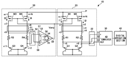
- FIG. 2 is a circuit block diagram illustrating a detailed configuration of the temperature measurement device 10 .
- the sensor 20 includes bipolar transistors Q 1 and Q 2 (referred to below as transistor Q 1 , transistor Q 2 ) as a pair of semiconductor elements with pn junctions.
- the transistors Q 1 and Q 2 are, for example, pnp transistors.
- the transistors Q 1 and Q 2 may be npn transistors. It is also possible to employ diodes in place of bipolar transistors.
- the bases and collectors of the transistors Q 1 and Q 2 are respectively connected to a common potential (for example to ground potential).
- the emitter of the transistor Q 1 is connected to a resistor element R 1
- the emitter of the transistor Q 2 is connected to a resistor element R 2 .
- the transistor Q 1 is an example of a first semiconductor element of technology disclosed herein, and the transistor Q 2 is an example of a second semiconductor element of technology disclosed herein.
- the resistor element R 1 is an example of a first resistor element of technology disclosed herein, and the second resistor element R 2 is an example of a second resistor element of technology disclosed herein.
- Field effect transistors M 1 and M 2 are, for example, p-channel MOSFETs.
- the sources of the transistors M 1 and M 2 are respectively connected to power source line P, and the gates of the transistors M 1 and M 2 that are the current control terminals are connected to an output terminal 59 of an operational amplifier 53 of the current source 50 .
- the transistor M 1 outputs a current I 1 (of current value i 1 ) according to a control voltage Vamp supplied to its own gate from the operational amplifier 53 .
- the transistor M 2 outputs a current I 2 (of current value i 2 ) according to a control voltage Vamp supplied to its own gate from the operational amplifier 53 .
- the transistor M 2 has a configuration in which N transistors that are similar to the transistor M 1 are connected together in parallel.
- the transistors M 1 , M 2 are examples of a first current output section of technology disclosed herein.
- a first connection switching section 21 is provided between the transistors M 1 and M 2 , and the resistor elements R 1 and R 2 .
- the first connection switching section 21 switches the connection destination of nodes n 1 and n 2 of the drains of the transistors M 1 , M 2 according to a control signal C 1 supplied from the controller 60 .
- the node n 1 is connected to a node n 3 on the high potential side of the resistor element R 1
- the node n 2 is connected to a node n 4 on the high potential side of the second resistor element R 2 .
- the first connection switching section 21 is an example of a first connection switching section of technology disclosed herein.
- a second connection switching section 22 selectively connects the nodes n 3 , n 4 and nodes n 5 , n 6 of the emitters of the transistors Q 1 , Q 2 (on the low voltage side of the resistor elements R 1 , R 2 ) to each of the input terminals of the AD converter 30 according to the control signal C 2 supplied from the controller 60 .
- the second connection switching section 22 is an example of a second connection switching section according to technology disclosed herein.
- the AD converter 30 includes a positive side input terminal 31 , a negative side input terminal 32 , and a reference voltage input terminal 33 .
- the AD converter 30 outputs a digital value expressing the difference between the voltage of the node connected to the positive side input terminal 31 and the voltage of the node connected to the negative side input terminal 32 , as a ratio to the reference voltage input to the reference voltage input terminal 33 .
- Output from the AD converter 30 is effected by a control signal C 3 supplied from the controller 60 .
- the digital value output from the AD converter 30 is supplied to the digital operation section 40 .
- the AD converter 30 may, for example, be a single bit delta-sigma modulation AD converter.
- a single bit delta-sigma modulation AD converter has the characteristics of good linearity, and relatively small circuit surface area for its resolution.
- the AD converter 30 is an example of an AD converter of technology disclosed herein.
- the digital operation section 40 computes a temperature measurement value T by performing computation processing on the digital value output from the AD converter 30 .
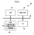
- FIG. 3 is a block diagram illustrating a detailed configuration of the digital operation section 40 .
- the digital operation section 40 is configured including a computer, and includes a Central Processing Unit (CPU) 41 , a register 42 , Read Only Memory (ROM) 43 , and an input/output port (I/O) 45 .
- the CPU 41 , the register 42 , the ROM 43 , and the input/output port I/O 45 are connected together through a bus 46 .
- the digital value output from the AD converter 30 is imported into the digital operation section 40 through the input/output port (I/O) 45 , and stored in the register 42 .
- a temperature computation program 44 for computing the temperature measurement value T is stored in the ROM 43 .
- the CPU 41 starts performing computation processing using the digital value stored in the register 42 by executing the temperature computation program 44 , and computes the temperature measurement value T.
- the computed temperature measurement value T is externally output through the input/output port (I/O) 45 . Details regarding the temperature computation program 44 are given below.
- the digital operation section 40 is an example of an operation section of technology disclosed herein.
- the register 42 is an example of a storage section of technology disclosed herein.
- the current source 50 includes a pair of bipolar transistors Q 3 and Q 4 (referred to below as transistor Q 3 and transistor Q 4 ) as a pair of semiconductor elements with pn junctions.
- the transistors Q 3 and Q 4 are, for example, pnp transistors.
- the transistors Q 3 and Q 4 may be npn transistors. It is also possible to employ diodes in place of bipolar transistors.
- the bases and collectors of the transistors Q 3 and Q 4 are respectively connected to a common potential (for example to ground potential).
- the emitter of the transistor Q 3 is connected to a resistor element R 3
- the emitter of the transistor Q 4 is connected to a resistor element R 4 .
- the transistor Q 3 is an example of a third semiconductor element of technology disclosed herein
- the transistor Q 4 is an example of a fourth semiconductor element of technology disclosed herein.
- Field effect transistors M 3 and M 4 are, for example, p-channel MOSFETs.
- the sources of the transistors M 3 and M 4 are respectively connected to the power source line P, and the gates of the transistors M 3 and M 4 that are the current control terminals are connected to the output terminal 59 of the operational amplifier 53 .
- the transistor M 3 outputs a current I 3 (of current value i 3 ) according to a control voltage Vamp supplied to its own gate from the operational amplifier 53 .
- the transistor M 4 outputs a current I 4 (of current value i 4 ) according to a control voltage Vamp supplied to its own gate from the operational amplifier 53 .
- the transistor M 4 has a configuration in which N transistors that are similar to the transistor M 3 are connected together in parallel.
- the transistors M 3 , M 4 are examples of a second current output section of technology disclosed herein.
- a third connection switching section 51 is provided between the transistors M 3 and M 4 , and the resistor elements R 3 and R 4 .
- the third connection switching section 51 switches the connection destination of nodes n 7 and n 8 of the drains of the transistors M 3 , M 4 according to a control signal C 5 supplied from the controller 60 .
- the node n 7 is connected to a node n 9 on the high potential side of the resistor element R 3
- the node n 8 is connected to a node n 10 on the high potential side of the second resistor element R 4 .
- the node n 7 is connected to the node n 10
- the node n 8 is connected to the node n 9 .
- the third connection switching section 51 is an example of a third connection switching section of technology disclosed herein.
- a fourth connection switching section 52 selectively connects the nodes n 9 , n 10 and nodes n 11 , n 12 of the emitters of the transistors Q 3 , Q 4 to an inverting input terminal 57 and a non-inverting input terminal 58 of the operational amplifier 53 according to a control signal C 6 supplied from the controller 60 .
- a control signal C 6 supplied from the controller 60 .
- the fourth connection switching section 52 is an example of a fourth connection switching section of technology disclosed herein.
- the operational amplifier 53 includes the inverting input terminal 57 connected through the fourth connection switching section 52 to one out of the transistors Q 3 and Q 4 , and the non-inverting input terminal 58 is connected to the other out of the transistors Q 3 and Q 4 .
- the operational amplifier 53 In the first current control state and the second current control state, the operational amplifier 53 generates an output voltage that controls the magnitudes of each of the currents I 1 to I 4 to correspond to the difference between the inter-base-emitter voltage of the transistor Q 3 and the inter-base-emitter voltage of the transistor Q 4 .
- the operational amplifier 53 outputs the output voltage from the output terminal 59 as control voltage Vamp.
- the output terminal 59 of the operational amplifier 53 is connected to the gates that are the current control terminals of the transistors M 1 to M 4 .
- the transistors M 1 to M 4 output currents I 1 to I 4 of magnitude according to the control voltage Vamp supplied from the operational amplifier 53 .
- the operational amplifier 53 is an example of an operational amplifier of technology disclosed here
- the operational amplifier 53 includes an internal fifth connection switching section 56 .
- the fifth connection switching section 56 includes switches 54 and 55 that, based on a control signal C 7 supplied from the controller 60 , switch between outputting the control voltage Vamp in-phase or out-of-phase with respect to the non-inverting input terminal 58 .
- the switch 55 is in the ON state
- the switch 54 is in the OFF state.
- the magnitude of the control voltage Vamp increases as the potential input to the non-inverting input terminal 58 rises.
- the fifth connection switching section 56 is an example of a fifth connection switching section of technology disclosed herein.
- the controller 60 controls the sensor 20 , the AD converter 30 , the digital operation section 40 , and the current source 50 overall by supplying the control signals C 1 to C 7 thereto.
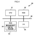
- FIG. 4 is a block diagram illustrating a detailed configuration of the controller 60 .
- the controller 60 is configured including a computer, and includes a Central Processing Unit (CPU) 61 , Random Access Memory (RAM) 62 , ROM 63 , and an input/output port (I/O) 65 .
- the CPU 61 , the RAM 62 , the ROM 63 , and the input/output port (I/O) 65 are connected together through a bus 66 .
- a measurement control program 64 is stored in the ROM 63 listing a cycle of processing to obtain the temperature measurement value T by controlling the sensor 20 , the AD converter 30 , the digital operation section 40 , and the current source 50 .
- the CPU 61 generates control signals C 1 to C 7 by executing the measurement control program 64 , and supplies the control signals to the sensor 20 , the AD converter 30 , the digital operation section 40 , and the current source 50 .
- the sensor 20 , the AD converter 30 , the digital operation section 40 , and the current source 50 are operated according to the control signals C 1 to C 7 supplied from the controller 60 .
- Plural digital values are thereby output from the AD converter 30 , and the temperature measurement value T computed based on the plural digital values is output from the digital operation section 40 .
- FIG. 5 illustrates an example of connection states in the temperature measurement device 10 .
- the node n 1 and the node n 3 , and the node n 2 and the node n 4 , of the sensor 20 are respectively connected together by the first connection switching section 21 .
- the node n 5 of the sensor 20 is connected to the negative side input terminal 32 of the AD converter 30
- the node n 6 of the sensor 20 is connected to the positive side input terminal 31 of the AD converter 30 , by the second connection switching section 22 .
- the node in which the current I 2 with the larger current value flows from out of the nodes n 5 and n 6 is connected to the reference voltage input terminal 33 of the AD converter 30 . Namely, in the example illustrated in FIG.
- the node n 6 is connected by the second connection switching section 22 to the reference voltage input terminal 33 of the AD converter 30 .
- the node n 7 and the node n 9 , and the node n 8 and the node n 10 , of the current source 50 are respectively connected together by the third connection switching section 51 .
- the node n 9 of the current source 50 is connected to the non-inverting input terminal 58 of the operational amplifier 53
- the node n 12 is connected to the inverting input terminal 57 of the operational amplifier 53 , by the fourth connection switching section 52 .
- the example illustrated in FIG. 5 is of an ON state of the switch 55 of the fifth connection switching section 56 .
- the control voltage Vamp that is the output voltage from the operational amplifier 53 is thereby output in-phase.
- the current I 3 output from the transistor M 3 of the current source 50 flows in the resistor element R 3 and the transistor Q 3
- the current I 4 output from the transistor M 4 flows in the resistor element R 4 and the transistor Q 4
- the difference between the inter-base-emitter voltage of the transistor Q 4 (namely the voltage of the node n 12 ) and the inter-base-emitter voltage of the transistor Q 3 (namely the voltage of the node n 11 ) is denoted ⁇ Vbe 1
- the resistance value of the resistor element R 3 is denoted r 3 .
- the current value i 3 of the current I 3 and the current value i 4 of the current I 4 are expressed by the following Equation (1) and Equation (2), respectively.
- the operational amplifier 53 outputs the control voltage Vamp that satisfies Equation (1).
- N in Equation (2) is a current ratio between the current I 3 and the current I 4 (i 4 /i 3 ), and is determined by the configuration of the transistors M 3 and M 4 .
- the current values i 3 and i 4 are proportional to ⁇ Vbe 1 , and do not depend on the magnitude of the voltage of power source line P.
- the control voltage Vamp output from the operational amplifier 53 is also supplied to the gates of the transistors M 1 and M 2 of the sensor 20 .
- the current value it of the current I 1 and the current value i 2 of the current I 2 are also proportional to ⁇ Vbe 1 , and do not depend on the magnitude of the voltage of the power source line P.
- the operational amplifier 53 generates the control voltage Vamp that controls the magnitudes of the current values i 1 to i 4 of the currents I 1 to I 4 to be proportional to ⁇ Vbe 1 , and supplies the control voltage Vamp to the gates of the transistors M 1 to M 4 .
- the currents I 1 to I 4 are currents with no dependency on the source voltage.
- the current I 1 output from the transistor M 1 of the sensor 20 flows in the resistor element R 1 and the transistor Q 1
- the current I 2 output from the transistor M 2 flows in the resistor element R 2 and the transistor Q 2
- the current I 1 flows in the forward direction with respect to the pn junction of the transistor Q 1
- the current I 2 flows in the forward direction with respect to the pn junction of the transistor Q 2
- the difference between the inter-base-emitter voltage of the transistor Q 2 namely the voltage of the node n 6
- the inter-base-emitter voltage of the transistor Q 1 namely the voltage of the node n 5
- the ⁇ Vbe is the difference between the forward direction voltage at the pn junction of the transistor Q 2 , and the forward direction voltage at the pn junction of the transistor Q 1 .
- the inter-base-emitter voltage of the transistor Q 2 in which the larger current value current I 2 out of the currents I 1 and I 2 flows (namely the voltage of the node n 6 ) is denoted Vbe. This thereby enables the temperature measurement value T (° C.) to be expressed by the following Equation (3) and Equation (4).
- A, B, and g are constants in Equation (3) and Equation (4).
- Vbe is a value that decreases with temperature rise.
- ⁇ Vbe is a value that increases with temperature rise.
- the denominator of Equation (3) can accordingly be made constant by setting an appropriate value for coefficient g.
- Equation (3) is proportional to the absolute temperature
- denominator of Equation (3) means that the fraction of Equation (3) is proportional to absolute temperature.
- the optimum constants A, B, g may be set in Equation (3) in consideration of the linearity of temperature conversion, and it is not always necessary to make the denominator constant with temperature.
- Equation (4) is a modified version of Equation (3).
- the digital value output from the AD converter 30 is the ratio of the measured voltage (the voltage difference between the positive side input terminal 31 and the negative side input terminal 32 ) to the voltage input to the reference voltage input terminal 33 .
- the digital value output from the AD converter 30 is equivalent to ⁇ Vbe/Vbe.
- applying the output value of the AD converter 30 to ⁇ Vbe/Vbe in Equation (4) enables the temperature measurement value T to be obtained.
- the temperature measurement value T is thereby obtainable by employing a digital value output from the AD converter 30 equivalent to ⁇ Vbe/Vbe, and performing the computation of Equation (4) in the digital operation section 40 .
- the pair of transistors Q 1 and Q 2 in the sensor 20 have equivalent inter-base-emitter voltages when current of the same magnitude flows therein.
- the mismatch between the transistors Q 1 and Q 2 in [1] means there is a difference in current characteristics of the inter-base-emitter voltage between the transistors Q 1 and Q 2 .
- the resistance values of the resistor elements R 1 and R 2 of the sensor 20 are equivalent to each other.
- a mismatch between the resistor elements R 1 and R 2 in [2] means there is a difference between the resistance value of the resistor element R 1 and the resistance value of the resistor element R 2 .
- a current ratio between the current I 1 output from the transistor M 1 of the sensor 20 and the current I 2 output from the transistor M 2 of the sensor 20 is a set current ratio (1:N).
- the mismatch between the transistor M 1 and the transistor M 2 in [3] means that there is deviation of the current ratio between current I 1 and current I 2 from the set current ratio (1:N).
- the AD converter 30 has no offset.
- the offset of the AD converter 30 in [ 4 ] is a digital value output from the AD converter 30 when the voltage difference between the positive side input terminal 31 and the negative side input terminal 32 is zero.
- the current values of the currents I 1 and I 2 in the sensor 20 are preferably controlled to a specific magnitude.
- the pair of transistors Q 3 and Q 4 of the current source 50 ideally have equivalent inter-base-emitter voltages when current of the same magnitude flows therein.
- a mismatch between the transistors Q 3 and Q 4 in [5] means there is a difference between the current characteristics of the inter-base-emitter voltages of the transistors Q 3 and Q 4 .
- the resistance values of the resistor elements R 3 and R 4 of the current source 50 are ideally equivalent to each other.
- a mismatch between the resistor elements R 3 and R 4 in [6] means there is a difference between the resistance value of the resistor R 3 and the resistance value of the resistor R 4 .
- the offset of the operational amplifier 53 in [7] is the output voltage output from the operational amplifier 53 when the voltage difference between the inverting input terminal 57 and the non-inverting input terminal 58 is zero.
- the temperature measurement device 10 performs the following processing to reduce errors arising in the temperature measurement value T due to cause [1] and cause [2].
- the temperature measurement device 10 measures the ⁇ Vbe in a first sensing state in which the current I 1 is being supplied to the resistor element R 1 and the transistor Q 1 , and the current I 2 is being supplied to the resistor element R 2 and the transistor Q 2 .
- the first sensing state the current I 1 flows in the forward direction with respect to the pn junction of the transistor Q 1
- the current I 2 flows in the forward direction with respect to the pn junction of the transistor Q 2 .
- the temperature measurement device 10 also measures the ⁇ Vbe in the second sensing state in which the current I 1 is supplied to the resistor element R 2 and the transistor Q 2 and the current I 2 is supplied to the resistor element R 1 and the transistor Q 1 .
- the current I 1 flows in the forward direction with respect to the pn junction of the transistor Q 2
- the current I 2 flows in the forward direction with respect to the pn junction of the transistor Q 1
- the ⁇ Vbe is the difference between the forward direction voltage at the pn junction of the transistor Q 1 (the inter-base-emitter voltage, the voltage at node n 5 ) and the forward direction voltage at the pn junction of the transistor Q 2 (the inter-base-emitter voltage, the voltage at node n 6 ).
- the temperature measurement device 10 computes the temperature measurement value T based on the average value of the ⁇ Vbe measured under the first sensing state and the ⁇ Vbe measured under the second sensing state. Taking the average of the value of each of the ⁇ Vbe obtained by switching over the supply destination of the current I 1 and I 2 in this manner enables error in the temperature measurement value T caused by mismatch between the transistors Q 1 and Q 2 and mismatch between the resistor elements R 1 and R 2 to be reduced.
- the temperature measurement device 10 performs the following processing to reduce errors arising in the temperature measurement value T due to cause [ 3 ].
- the temperature measurement device 10 measures the voltages across the two ends of the resistor elements R 1 and R 2 in both the first sensing state and the second sensing state.
- ⁇ Vbe may be approximated here using the characteristic of the pn junction in the following Equation (5).
- Equation (5) k B is the Boltzmann constant, T a (K) is the absolute temperature, and q is the elementary charge.
- Equation (6) is obtained, wherein ⁇ Vbe and C are denoted ⁇ Vbeo and Co, respectively, when there is no mismatch between the transistors M 1 and M 2 .
- Equation ⁇ ⁇ ( 7 ) ⁇ ⁇ ⁇ Vbeo ⁇ ⁇ ⁇ Vbe ⁇ log ⁇ ( Co ) log ⁇ ( C ) ( 7 )
- Co in the Equation (6) and the Equation (7) is a value equivalent to the design value of current ratio (1:N) between the current I 1 and I 2 .
- the temperature measurement device 10 computes ⁇ Vbeo in which the effect of mismatch between the transistors M 1 and M 2 is reduced by correcting the measured ⁇ Vbe using the correction coefficient K.
- the temperature measurement device 10 then computes the temperature measurement value T based on the ⁇ Vbeo.
- An AD conversion value corresponding to the voltage difference between the node n 5 and the node n 6 in the first sensing state ( ⁇ Vbe) is denoted D 1
- the AD conversion value corresponding to the voltage difference between the node n 5 and the node n 6 in the second sensing state ( ⁇ Vbe) is denoted D 2
- the AD conversion value corresponding to the offset voltage of the AD converter 30 is denoted D OFFSET .
- D 1S The AD conversion value corresponding to the measurement value of the voltage difference between the node n 5 and the node n 6 ( ⁇ Vbe) in the first sensing state and including the offset voltage of the AD converter 30 is denoted D 1S .
- Equation (11) implies that the offset voltage of the AD converter 30 can be eliminated by acquiring an AD conversion value D 1S acquired in the first sensing state with opposite polarity to the AD conversion value D 2S acquired in the second sensing state.
- the temperature measurement device 10 accordingly performs the following processing to reduce the error in the temperature measurement value T caused by cause [4].
- the temperature measurement device 10 switches the connections to the positive side input terminal 31 and the negative side input terminal 32 of the AD converter 30 using the second connection switching section 22 such that the polarities of the ⁇ Vbe measured in each of the states of the first sensing state and the second sensing state are the opposite of each other.
- the temperature measurement device 10 performs the following processing.
- the temperature measurement device 10 measures the ⁇ Vbe in the first current control state, in which the current I 3 is supplied to the resistor element R 3 and the transistor Q 3 and the current I 4 is supplied to the resistor element R 4 and the transistor Q 4 .
- the temperature measurement device 10 also measures the ⁇ Vbe in the second current control state in which the current I 3 is supplied to the resistor element R 4 and the transistor Q 4 , and the current I 4 is supplied to the resistor element R 3 and the transistor Q 3 .
- the transition in state between the first current control state and the second current control state is performed by the third connection switching section 51 .
- the temperature measurement device 10 computes the temperature measurement value T based on the average value of the ⁇ Vbe measured under each of the states of the first current control state and the second current control state. This thereby enables errors in the temperature measurement value T caused by the mismatch between the transistors Q 3 and Q 4 and the mismatch between the resistor elements R 3 and R 4 to be reduced by taking the average value of each of the values of ⁇ Vbe obtained under each of the current control states in which the supply destination of the currents I 3 and I 4 are switched.
- the temperature measurement device 10 performs the following processing in order to reduce errors in the temperature measurement value T caused by cause [7].
- the temperature measurement device 10 along with transitioning states between the first current control state and the second current control state, also switches the nodes connected to the inverting input terminal 57 and the non-inverting input terminal 58 of the operational amplifier 53 . Namely, the temperature measurement device 10 connects the node positioned symmetrically to the node connected to the inverting input terminal 57 in the first current control state to the non-inverting input terminal 58 in the second current control state.
- the temperature measurement device 10 also connects the node positioned symmetrically to the node connected to the non-inverting input terminal 58 in the first current control state to the inverting input terminal 57 in the second current control state. Switching over the nodes connected to the inverting input terminal 57 and the non-inverting input terminal 58 is performed in the temperature measurement device 10 by the fourth connection switching section 52 .
- the temperature measurement device 10 also, along with transitioning states between the first current control state and the second current control state, switches the phase of the output voltage of the operational amplifier 53 between in-phase and out-of-phase with respect to the non-inverting input terminal 58 .
- Switching the input and output of the operational amplifier 53 as described above at the same time as transitioning states between the first current control state and the second current control state makes the operation of the current source 50 overall equivalent in each of the states.
- switching of the phase of the output voltage between in-phase and out-of-phase with respect to the non-inverting input terminal 58 is performed by the fifth connection switching section 56 .
- the temperature measurement value T is computed based on the average value of the measured ⁇ Vbe under each state of the first current control state and the second current control state. This thereby enables a reduction in the error in temperature measurement value T caused by offset of the operation amplifier 53 .
- FIG. 6 and FIG. 7 are flowcharts illustrating a flow of measurement control processing implemented by the CPU 61 of the controller 60 executing the measurement control program 64 (see FIG. 4 ) stored in the ROM 63 .
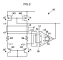
- step S 1 the CPU 61 of the controller 60 transitions the current source 50 to the first current control state by supplying the control signals C 5 to C 7 to the respective third to fifth connection switching sections 51 , 52 , 56 of the current source 50 .
- FIG. 8 is a circuit block diagram illustrating a connection state of the current source 50 in the first current control state.
- the third connection switch 51 connects the node n 7 to the node n 9 , and connects the node n 8 to the node n 10 .
- the fourth connection switching section 52 connects the node n 9 to the non-inverting input terminal 58 of the operational amplifier 53 , and connects the node n 12 to the inverting input terminal 57 of the operational amplifier 53 .
- the fifth connection switching section 56 places the switch 55 in an ON state and the switch 54 in an OFF state so as to output the output voltage of the operational amplifier 53 in-phase with respect to the non-inverting input terminal 58 .
- the current I 3 output from the transistor M 3 flows in the resistor element R 3 and the transistor Q 3
- the current I 4 output from the transistor M 4 flows in the resistor element R 4 and the transistor Q 4 .
- the current value I 3 flows in the forward direction with respect to the pn junction of the transistor Q 3
- the current I 4 flows in the forward direction with respect to the pn junction of the transistor Q 4 .
- the operational amplifier 53 outputs the control voltage Vamp that controls the magnitudes of each of the current values of the currents I 1 to I 4 to correspond to the difference between the forward direction voltage in the pn junction of the transistor Q 3 and the forward direction voltage in the pn junction of the transistor Q 4 in-phase with respect to the non-inverting input terminal 58 .
- Each of the current values of the currents I 1 to I 4 is thereby controlled to as to be constant, and not to depend on the voltage of the power source line P. Namely, the currents I 1 to I 4 become currents that do not depend on the power source voltage.
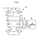
- step S 2 the CPU 61 of the controller 60 transitions the sensor 20 to the first sensing state by supplying the control signal C 1 to the first connection switching section 21 of the sensor 20 .
- the CPU 61 of the controller 60 forms connections to measure the voltage across the two ends of the resistor element R 1 as a negative voltage in the AD converter 30 by supplying the control signal C 2 to the second connection switching section 22 of the sensor 20 .
- FIG. 9 is a circuit block diagram illustrating a connected state in the first sensing state, in which the voltage across the two ends of the resistor element R 1 is measured as a negative voltage in the AD converter 30 .
- the first connection switching section 21 connects the node n 1 to the node n 3 , and the node n 2 to the node n 4 when the sensor 20 is in the first sensing state. This thereby enables the current I 1 output from the transistor M 1 to flow in the resistor element R 1 and the transistor Q 1 , and the current I 2 output from the transistor M 2 to flow in the resistor element R 2 and the transistor Q 2 .
- the current I 1 flows in the forward direction with respect to the pn junction of the transistor Q 1
- the current I 2 flows in the forward direction with respect to the pn junction of the transistor Q 2 .
- the second connection switching section 22 connects the node n 5 to the positive side input terminal 31 of the AD converter 30 , and connects the node n 3 to the negative side input terminal 32 of the AD converter 30 when the voltage across the two ends of the resistor element R 1 is measured as a negative voltage in the AD converter 30 .
- the second connection switching section 22 connects the node n 6 in which the current I 2 is flowing to the reference voltage input terminal 33 of the AD converter 30 .
- step S 4 output from the AD converter 30 is effected by the CPU 61 of the controller 60 supplying the control signal C 3 to the AD converter 30 .
- the AD converter 30 thereby outputs the negative digital value V 1 corresponding to the voltage across the two ends of the resistor element R 1 .
- import of the digital value V 1 output from the AD converter 30 is instructed by the CPU 61 of the controller 60 by supplying the control signal C 4 to the digital operation section 40 .
- the digital operation section 40 thereby stores the digital value V 1 output from the AD converter 30 in its own register 42 .
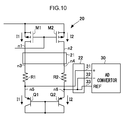
- the CPU 61 of the controller 60 forms connections to measure the voltage difference, ⁇ Vbe, between the nodes n 5 and n 6 as a negative voltage in the AD converter 30 by supplying the control signal C 2 to the second connection switching section 22 of the sensor 20 .
- the ⁇ Vbe is the difference between the forward direction voltage in the pn junction of the transistor Q 1 (inter-base-emitter voltage), and the forward direction voltage in the pn junction of the transistor Q 2 (inter-base-emitter voltage).
- FIG. 10 is a circuit block diagram illustrating the connection state in the first sensing state, in which ⁇ Vbe is measured as a negative voltage in the AD converter 30 .
- the second connection switching section 22 connects the node n 5 to the positive side input terminal 31 of the AD converter 30 , and the node n 6 to the negative side input terminal 32 of the AD converter 30 when the ⁇ Vbe is being measured as a negative voltage in the AD converter 30 in the first sensing state.
- the node n 6 is maintained in a connected state to the reference voltage input terminal 33 of the AD converter 30 .
- step S 6 output from the AD converter 30 is effected by the CPU 61 of the controller 60 supplying the control signal C 3 to the AD converter 30 .
- the AD converter 30 thereby outputs the negative digital value V 2 corresponding to the ⁇ Vbe.
- import of the digital value V 2 output from the AD converter 30 is instructed by the CPU 61 of the controller 60 by supplying the control signal C 4 to the digital operation section 40 .
- the digital operation section 40 thereby stores the digital value V 2 output from the AD converter 30 in its own register 42 .
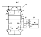
- the CPU 61 of the controller 60 forms connections to measure the voltage across the two ends of the resistor element R 2 as a negative voltage in the AD converter 30 by supplying the control signal C 2 to the second connection switching section 22 of the sensor 20 .
- FIG. 11 is a circuit block diagram illustrating a connection state in the first sensing state when measuring the voltage across the two ends of the resistor element R 2 as a negative voltage in the AD converter 30 .
- the second connection switching section 22 connects the node n 6 to the positive side input terminal 31 of the AD converter 30 , and connects the node n 4 to the negative side input terminal 32 of the AD converter 30 .
- the node n 6 is maintained in a connected state to the reference voltage input terminal 33 of the AD converter 30 .
- step S 8 output of the AD converter 30 is effected by the CPU 61 of the controller 60 supplying the control signal C 3 to the AD converter 30 .
- the AD converter 30 thereby outputs the negative digital value V 3 corresponding to the voltage across the two ends of the resistor element R 2 .
- the CPU 61 of the controller 60 instructs import of the digital value V 3 output from the AD converter 30 by supplying the control signal C 4 to the digital operation section 40 .
- the digital operation section 40 thereby stores the digital value V 3 output from the AD converter 30 in its own register 42 .
- step S 9 the CPU 61 of the controller 60 transitions the sensor 20 to the second sensing state by supplying the control signal C 1 to the first connection switching section 21 of the sensor 20 .
- the CPU 61 of the controller 60 forms connections to measure the voltage across the two ends of the resistor element R 1 as a positive voltage in the AD converter 30 by supplying the control signal C 2 to the second connection switching section 22 of the sensor 20 .
- FIG. 12 is a circuit block diagram illustrating a connection state when measuring the voltage across the two ends of the resistor element R 1 as a positive voltage in the AD converter 30 in the second sensing state.
- the first connection switching section 21 connects the node n 1 to the node n 4 , and connects the node n 2 to the node n 3 .
- the current I 1 output from the transistor M 1 thereby flows in the resistor element R 2 and the transistor Q 2
- the current I 2 output from the transistor M 2 flows in the resistor element R 1 and the transistor Q 1 .
- the current I 1 flows in the forward direction with respect to the pn junction of the transistor Q 2
- the current I 2 flows in the forward direction with respect to the pn junction of the transistor Q 1 .
- the second connection switching section 22 When measuring the voltage across the two ends of the resistor element R 1 as a positive voltage in the AD converter 30 , the second connection switching section 22 connects the node n 3 to the positive side input terminal 31 of the AD converter 30 and connects the node n 5 to the negative side input terminal 32 of the AD converter 30 . In the second sensing state, out of the node n 5 and the node n 6 , the second connection switching section 22 connects the node n 5 in which the current I 2 flows to the reference voltage input terminal 33 of the AD converter 30 .
- step S 11 output of the AD converter 30 is effected by the CPU 61 of the controller 60 supplying the control signal C 3 to the AD converter 30 .
- the AD converter 30 thereby outputs the positive digital value V 4 corresponding to the voltage across the two ends of the resistor element R 1 .
- the CPU 61 of the controller 60 instructs import of the digital value V 4 output from the AD converter 30 by supplying the control signal C 4 to the digital operation section 40 .
- the digital operation section 40 thereby stores the digital value V 4 output from the AD converter 30 in its own register 42 .
- the CPU 61 of the controller 60 forms connections to measure the voltage difference between the node n 5 and the node n 6 , ⁇ Vbe, as a positive voltage in the AD converter 30 by supplying the control signal C 2 to the second connection switching section 22 of the sensor 20 .
- the ⁇ Vbe is the difference between the forward direction voltage (the inter-base-emitter voltage) in the pn junction of the transistor Q 1 and the forward direction voltage (the inter-base-emitter voltage) in the pn junction of the transistor Q 2 .
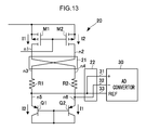
- FIG. 13 is a circuit block diagram illustrating a connection state when measuring the ⁇ Vbe as a positive voltage in the AD converter 30 in the second sensing state.
- the second connection switching section 22 connects the node n 5 to the positive side input terminal 31 of the AD converter 30 , and connects the node n 6 to the negative side input terminal 32 of the AD converter 30 .
- the node n 5 is maintained in a connected state to the reference voltage input terminal 33 of the AD converter 30 .
- step S 13 output from the AD converter 30 is effected by the CPU 61 of the controller 60 supplying the control signal C 3 to the AD converter 30 .
- the AD converter 30 thereby outputs the positive digital value V 5 corresponding to the ⁇ Vbe.
- the CPU 61 of the controller 60 instructs import of the digital value V 5 output from the AD converter 30 by supplying the control signal C 4 to the digital operation section 40 .
- the digital operation section 40 thereby stores the digital value V 5 output from the AD converter 30 in its own register 42 .
- the CPU 61 of the controller 60 forms connections for measuring the voltage across the two ends of the resistor element R 2 as a positive voltage in the AD converter 30 by supplying the control signal C 2 to the second connection switching section 22 of the sensor 20 .
- FIG. 14 is a circuit block diagram illustrating a connection state when measuring the voltage across the two ends of the resistor element R 2 as a positive voltage in the AD converter 30 in the second sensing state.
- the second connection switching section 22 connects the node n 4 to the positive side input terminal 31 of the AD converter 30 , and connects the node n 6 to the negative side input terminal 32 of the AD converter 30 .
- the node n 5 is maintained in a connected state to the reference voltage input terminal 33 of the AD converter 30 .
- step S 15 output from the AD converter 30 is effected by the CPU 61 of the controller 60 supplying the control signal C 3 to the AD converter 30 .
- the AD converter 30 thereby outputs the positive digital value V 6 corresponding to the voltage across the two ends of the resistor element R 2 .
- the CPU 61 of the controller 60 instructs import of the digital value V 6 output from the AD converter 30 by supplying the control signal C 4 to the digital operation section 40 .
- the digital operation section 40 thereby stores the digital value V 6 output from the AD converter 30 in its own register 42 .
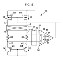
- step S 16 the CPU 61 of the controller 60 transitions the current source 50 to the second current control state by supplying the respective control signals C 5 to C 7 to the third to the fifth connection switching sections 51 , 52 , 56 of the current source 50 .
- FIG. 15 is a circuit block diagram illustrating a connection state of the current source 50 in the second current control state.
- the third connection switching section 51 connects the node n 7 to the node n 10 , and connects the node n 8 to the node n 9 .
- the fourth connection switching section 52 connects the node n 11 that is positioned symmetrically to the node n 12 connected to the inverting input terminal 57 in the first current control state, to the non-inverting input terminal 58 in the second current control state.
- the fourth connection switching section 52 connects the node n 10 that is positioned symmetrically to the node n 9 connected to the non-inverting input terminal 58 in the first current control state to the inverting input terminal 57 in the second current control state.
- the fifth connection switching section 56 places the switch 54 in the ON state, and places the switch 55 in the OFF state in order to output the output voltage of the operational amplifier 53 out-of-phase with respect to the non-inverting input terminal 58 .
- the current I 3 output from the transistor M 3 flows in the resistor element R 4 and the transistor Q 4 , and the current I 4 output from the transistor M 4 thereby flows in the resistor element R 3 and the transistor Q 3 .
- the current I 3 flows in the forward direction with respect to the pn junction of the transistor Q 4 , and the current I 4 flows in the forward direction with respect to the pn junction of the transistor Q 3 .
- the operational amplifier 53 outputs the control voltage Vamp that controls the magnitude of each of the current values of the currents I 1 to I 4 to correspond to the difference between the forward direction voltage in the pn junction of the transistor Q 3 and the forward direction voltage in the pn junction of the transistor Q 4 out-of-phase with respect to the non-inverting input terminal 58 .
- Each of the current values of the currents I 1 to I 4 is thereby controlled to as to be constant, and not to depend on the voltage of the power source line P. Namely, the currents I 1 to I 4 are currents that do not have a source voltage dependency.
- each of the steps S 17 to S 30 is similar to the processing of each of the steps S 2 to S 15 described above, and so detailed explanation thereof will be omitted.
- the negative digital value V 7 corresponding to the voltage across the two ends of the resistor element R 1 measured under the first sensing state is stored in the register 42 of the digital operation section 40 by executing the processing of step S 19 .
- the negative digital value V 8 corresponding to the ⁇ Vbe measured under the first sensing state is stored in the register 42 of the digital operation section 40 by executing the processing of step S 21 .
- the negative digital value V 9 corresponding to the voltage across the two ends of the resistor element R 2 measured under the first sensing state is stored in the register 42 of the digital operation section 40 by executing the processing of step S 23 .
- the positive digital value V 10 corresponding to the voltage across the two ends of the resistor element R 1 measured under the second sensing state is stored in the register 42 of the digital operation section 40 by executing the processing of step S 26 .
- the positive digital value V 11 corresponding to the ⁇ Vbe measured under the second sensing state is stored in the register 42 of the digital operation section 40 by executing the processing of step S 28 .
- the positive digital value V 12 corresponding to the voltage across the two ends of the resistor element R 2 measured under the second sensing state is stored in the register 42 of the digital operation section 40 by executing the processing of step S 30 .
- step S 31 start of the computation processing to compute the temperature measurement value T is instructed by the CPU 61 of the controller 60 supplying the control signal C 4 to the digital operation section 40 , then the present routine is ended.
- the sequence for acquiring the digital values V 1 to V 12 is not limited to the above sequence, and may be modified as appropriate.
- FIG. 16 is a diagram illustrating correspondence relationships between states of the sensor 20 and the current source 50 in the above measurement control processing (see FIG. 6 and FIG. 7 ), and voltages measured in the AD converter 30 and digital values corresponding to these voltages.
- the sensor 20 adopts the first sensing state and the second sensing state, respectively.
- the digital values V 1 to V 3 are acquired under the first current control state and the first sensing state
- the digital values V 4 to V 6 are acquired under the first current control state and the second sensing state.
- the digital values V 7 to V 9 are acquired under the second current control state and the first sensing state, and the digital values V 10 to V 12 are acquired under the second current control state and the second sensing state.
- the acquired digital values V 1 to V 12 are stored in the register 42 of the digital operation section 40 .
- the digital values V 2 and V 8 are examples of first digital values of technology disclosed herein.
- the digital values V 5 and V 11 are examples of second digital values of technology disclosed herein.
- the digital values V 1 and V 7 are examples of third digital values of technology disclosed herein.
- the digital values V 3 and V 9 are examples of fourth digital values of technology disclosed herein.
- the digital values V 4 and V 10 are examples of fifth digital values of technology disclosed herein.
- the digital values V 6 and V 12 are examples of sixth digital values of technology disclosed herein.
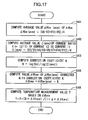
- FIG. 17 is a flowchart illustrating a flow of temperature computation processing implemented by the CPU 41 of the digital operation section 40 executing the temperature computation program 44 (see FIG. 3 ) stored in the ROM 43 .
- the digital operation section 40 starts execution of the temperature computation program according to the control signal C 4 supplied from the CPU 61 of the controller 60 .
- the CPU 41 of the digital operation section 40 computes the average value, ⁇ Vbe (aye), of the ⁇ Vbe measured under the first and the second current control states, and the first and the second sensing states. Namely, the CPU 41 reads the digital values V 2 , V 5 , V 8 , and V 11 corresponding to the ⁇ Vbe stored in the register 42 , and performs the computation processing represented by Equation (12) below.
- ⁇ ⁇ ⁇ Vbe ⁇ ( ave ) V ⁇ ⁇ 5 - V ⁇ ⁇ 2 + V ⁇ ⁇ 11 - V ⁇ ⁇ 8 4 ( 12 )
- Averaging the digital values V 2 and V 5 acquired under the first current control state reduces the effects of the mismatch between the transistors Q 1 and Q 2 (cause [1]) and the mismatch between the resistor elements R 1 and R 2 (cause [2]) of the sensor.
- the effect of the offset of the AD converter 30 (cause [4]) is reduced since the digital values V 2 and V 5 are acquired so as to have mutually opposite polarities in the AD converter 30 .
- Including the digital values V 8 and V 11 , acquired under the second current control state, in the average reduces the effects of the mismatch between the transistors Q 3 and Q 4 (cause [5]), and the mismatch between the resistors R 3 and R 4 (cause [6]). Since switching between the first current control state and the second current control state accompanies the switching of the input/output in the operational amplifier 53 , the effect of the offset of the operational amplifier 53 (cause [7]) is reduced.
- the digital values V 1 , V 6 , V 7 , and V 12 are values proportional to the current value it of the current I 1
- the digital values V 3 , V 4 , V 9 , and V 10 are values proportional to the current value i 2 of the current I 2
- V 3 /V 1 , V 4 /V 6 , V 9 /V 7 , and V 10 /V 12 each correspond to current ratio i 2 /i 1
- the effects of causes [1], [2], and [4] to [7] are reduced by averaging V 3 /V 1 , V 4 /V 6 , V 9 /V 7 , and V 10 /V 12 .
- the CPU 41 of the digital operation section 40 computes the correction coefficient K for correcting the ⁇ Vbe (aye) computed at step S 41 based on the average value C (ave) of the current ratios computed at step S 42 . Namely, the CPU 41 performs the computation processing represented by Equation (14) below.
- Co is the design value N of the current ratio (1:N) between the current I 1 and the current I 2 . Since a comparatively long computation time is needed for the logarithmic computation, the correction coefficient K may be computed using an first approximation equation corresponding to log(Co)/log(C (ave)). A decrease in computation time is thereby enabled compared to when the logarithmic computation is performed
- the CPU 41 of the digital operation section 40 computes the temperature measurement value T based on the corrected value ⁇ Vbeo computed at step S 44 . Namely, the CPU 41 performs the computation processing represented by Equation (16) below.
- T A + B ⁇ ⁇ ⁇ ⁇ Vbeo 1 + g ⁇ ⁇ ⁇ ⁇ Vbeo ( 16 )
- Equation (16) corresponds to Equations (3) and (4).
- circuit connections in the sensor 20 and the current source 50 are switched by the first to the fifth switching sections 21 , 22 , 51 , 52 , 56 , forming the first and the second current control states, and the first and the second sensing states.
- Each of the voltages measured by the AD converter 30 under each of the above states are stored in the digital operation section 40 as the digital values V 1 to V 12 .
- the digital operation section 40 computes the temperature measurement value T based on the stored digital values V 1 to V 12 .
- the digital operation section 40 computes the temperature measurement value T based on the stored digital values V 1 to V 12 .
- the plural states for acquiring the digital values V 1 to V 12 used in the computation processing in the digital operation section 40 are formed by switching of the circuit connections by the first to the fifth switching sections 21 , 22 , 51 , 52 , 56 .
- the temperature measurement value T for which the effects of mismatches and the like between respective elements are reduced is acquired by the digital operation section 40 performing digital computation processing based on the digital values V 1 to V 12 . Accordingly, according to the temperature measurement device 10 , enlargement of the circuit scale of an analog circuit can be avoided, and an increase in circuit surface area and an increase in power consumption can be avoided.
- the temperature measurement device 10 according to exemplary embodiments of technology disclosed herein enables an increase in temperature measurement precision to be achieved while suppressing an increase in circuit surface area.
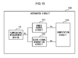
- FIG. 18 is a block diagram illustrating an example of a configuration of an integrated circuit 100 provided with the temperature measurement device 10 .
- the integrated circuit 100 includes the temperature measurement device 10 , a power source circuit 101 , a clock signal generation circuit 102 , and a computation circuit 103 .
- the integrated circuit 100 is an example of an integrated circuit of technology disclosed herein.
- the power source circuit 101 and the clock signal generation circuit 102 are examples of functional sections of technology disclosed herein.
- the computation circuit 103 is driven by a power source voltage Vs supplied from the power source circuit 101 , and synchronizes with a clock signal Sc supplied from the clock signal generation circuit 102 to perform computation processing.
- the temperature measurement device 10 supplies a temperature detection signal St indicating the temperature measurement value T computed in the digital operation section 40 (omitted from illustration in FIG. 18 ) to the power source circuit 101 and the clock signal generation circuit 102 .
- the power source circuit 101 changes the magnitude of the power source voltage Vs based on the temperature measurement value T indicated by the temperature detection signal St supplied from the temperature measurement device 10 .
- the power source circuit 101 for example, lowers the power source voltage Vs in response to an increase in the temperature measurement value T indicated by the temperature detection signal St.
- the clock signal generation circuit 102 changes the frequency of the clock signal Sc based on the temperature detection signal St supplied from the temperature measurement device 10 .
- the clock signal generation circuit 102 for example, lowers the frequency of the clock signal Sc in response to an increase in the temperature measurement value T indicated by the temperature detection signal St.
- the temperature measurement device 10 may take the form of a stand-alone integrated circuit (IC), and may be widely employed in applications in which temperature is measured by the IC.
- IC stand-alone integrated circuit
- the processing in the temperature measurement device 10 may be simplified by addressing only some of the causes [1] to [7].
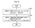
- FIG. 19 is a flowchart illustrating a flow of computation processing, implemented by the CPU 41 of the digital operation section 40 , according to a first modified example.
- step S 51 the CPU 41 of the digital operation section 40 reads the digital values V 2 , V 5 corresponding to the ⁇ Vbe stored in the register 42 , and performs the computation processing represented by Equation (17) below.
- the CPU 41 of the digital operation section 40 computes the temperature measurement value T based on the corrected value ⁇ Vbe (aye) computed at step S 51 . Namely, the CPU 41 performs the computation processing represented by Equation (18) below.
- T A + B ⁇ ⁇ ⁇ ⁇ Vbe ⁇ ( ave ) 1 + g ⁇ ⁇ ⁇ ⁇ Vbe ⁇ ( ave ) ( 18 )
- the effects of the mismatch between the transistors Q 1 and Q 2 of the sensor 20 (cause [1]), and the mismatch between the resistor elements R 1 and R 2 of the sensor 20 (cause [2]), are reduced in the temperature measurement value T.
- the effect of the offset of the AD converter 30 (cause [4]) is also reduced in the temperature measurement value T.
- processing for acquiring the digital values other than the digital values V 2 and V 5 may be omitted from the above measurement control processing (see FIG. 6 , and FIG. 7 ) as appropriate.
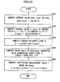
- FIG. 20 is a flowchart illustrating a flow of temperature computation processing, implemented by the CPU 41 of the digital operation section 40 , according to a second modified example.
- the CPU 41 of the digital operation section 40 reads the digital values V 2 , V 5 corresponding the ⁇ Vbe stored in the register 42 , and computes ⁇ Vbe (ave) by performing the computation processing represented by Equation (17).
- the CPU 41 of the digital operation section 40 reads the digital values V 1 , V 3 , V 4 , V 6 stored in the register 42 , and computes the average value C (ave) of the current ratio between the current I 1 and the current I 2 by performing the computation processing represented by Equation (19) below.
- the digital operation section 40 of the CPU 41 computes the correction coefficient K for correcting the ⁇ Vbe (ave) computed at step S 61 , based on the average value C (ave) of the current ratio computed at step S 62 . Namely, the CPU 41 performs the computation processing represented by the above Equation (14).
- the CPU 41 of the digital operation section 40 computes the corrected value ⁇ Vbeo of the ⁇ Vbe (ave) computed at step S 61 using the correction coefficient K computed at step 63 . Namely, the CPU 41 performs the computation processing represented by Equation (15) above.
- the CPU 41 of the digital operation section 40 computes the temperature measurement value T based on the corrected value ⁇ Vbeo computed at step S 64 . Namely, the CPU 41 performs the computation processing represented by Equation (16) above.
- the effects of the mismatch between the transistors Q 1 and Q 2 of the sensor 20 (cause [1]), and the mismatch between the resistor elements R 1 and R 2 of the sensor 20 (cause [2]), are reduced in the temperature measurement value T.
- the effects of the mismatch between the transistors M 1 and M 2 (cause [3]), and the offset of the AD converter 30 (cause [4]) are also reduced in the temperature measurement value T.
- the processing for acquiring the digital values other than the digital values V 1 to V 6 may be omitted from the above measurement control processing (see FIG. 6 , and FIG. 7 ) as appropriate.
- the digital operation section 40 and the controller 60 that configure the temperature measurement device 10 according to the first exemplary embodiment above include a computer that includes a CPU, and the temperature computation processing and the measurement control processing above are implemented by software.
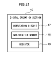
- a digital operation section 40 and a controller 60 according to the second exemplary embodiment implement the respective temperature computation processing and measurement control processing using hardware logic.
- FIG. 21 is a block diagram illustrating an example of a configuration of the digital operation section 40 according to the second exemplary embodiment in which the above temperature computation processing is implemented by hardware logic.
- the digital operation section 40 according to the second exemplary embodiment includes a computation circuit 47 , non-volatile memory 48 , and a resistor 49 .
- the computation circuit 47 is a hardware logic circuit that performs predetermined logical computations for computing the temperature measurement value T.
- the non-volatile memory 48 is a recording medium that stores a conversion coefficient for computing the temperature measurement value T.
- the non-volatile memory 48 may, for example, be a programmable e-fuse.
- the non-volatile memory 48 may be omitted when the conversion coefficient is a fixed value.
- the resistor 49 is a storage circuit that holds digital values output from the AD converter 30 .
- the above temperature computation processing implemented by software in the first exemplary embodiment, can be implemented by hardware logic.
- the controller 60 has the configuration below for implementing the above measurement control processing using hardware logic.
- the controller 60 for example, includes a counter, the control circuit that controls switching timing of the circuit connections in the first to the fifth switching sections 21 , 22 , 51 , 52 , 56 , and an interface circuit for performing communication with the digital operation section 40 (all of which are omitted from illustration).
- An aspect of technology disclosed herein exhibits the advantageous effect of enabling an increase in temperature measurement precision to be achieved in a temperature measurement device while suppressing an increase in circuit surface area.
Landscapes
- Physics & Mathematics (AREA)
- General Physics & Mathematics (AREA)
- Engineering & Computer Science (AREA)
- Theoretical Computer Science (AREA)
- Measuring Temperature Or Quantity Of Heat (AREA)
- Amplifiers (AREA)
Abstract
Description
- ISSCC 2005/
SESSION 13/SENSORS/13.1 “A CMOS Temperature Sensor with a 3σ Inaccuracy of ±0.1° C. from −55° C. to 125° C.” by Michiel Pertijs, Kofi Makinwa and Johan Huij sing.
Wherein A, B, and g are constants in Equation (3) and Equation (4). In Equation (3), Vbe is a value that decreases with temperature rise. ΔVbe is a value that increases with temperature rise. The denominator of Equation (3) can accordingly be made constant by setting an appropriate value for coefficient g. Moreover, ΔVbe is proportional to the absolute temperature, and so making denominator of Equation (3) constant with temperature means that the fraction of Equation (3) is proportional to absolute temperature. Thus setting appropriate values for the constants A, B, g in Equation (3) to enable the temperature measurement value T to be obtained. The optimum constants A, B, g may be set in Equation (3) in consideration of the linearity of temperature conversion, and it is not always necessary to make the denominator constant with temperature.
ΔVbeo in Equation (5) and Equation (6) can be expressed by the following Equation (7).
D 1S =D 1 +D OFFSET (8)
Equation (8)
D 2S =D 2 +D OFFSET (9)
Equation (9)
D 1 =−D 2 (10)
Equation (10)
In Equation (10), causes of deterioration in precision other than the offset of the
D 1S −D 2S =D 1 +D OFFSET−(D 2 +D OFFSET)=D 1 −D 2=2D 1 (11)
Equation (11)
ΔVbeo=ΔVbe(ave)×K (15)
Claims (19)
Applications Claiming Priority (2)
| Application Number | Priority Date | Filing Date | Title |
|---|---|---|---|
| JP2014066779A JP6379578B2 (en) | 2014-03-27 | 2014-03-27 | Temperature measuring apparatus, integrated circuit, and temperature measuring method |
| JP2014-066779 | 2014-03-27 |
Publications (2)
| Publication Number | Publication Date |
|---|---|
| US20150276497A1 US20150276497A1 (en) | 2015-10-01 |
| US9897490B2 true US9897490B2 (en) | 2018-02-20 |
Family
ID=54067098
Family Applications (1)
| Application Number | Title | Priority Date | Filing Date |
|---|---|---|---|
| US14/618,911 Active 2035-12-07 US9897490B2 (en) | 2014-03-27 | 2015-02-10 | Temperature measurement device, integrated circuit, and temperature measurement method |
Country Status (4)
| Country | Link |
|---|---|
| US (1) | US9897490B2 (en) |
| JP (1) | JP6379578B2 (en) |
| CN (1) | CN104949767B (en) |
| DE (1) | DE102015202520B4 (en) |
Cited By (1)
| Publication number | Priority date | Publication date | Assignee | Title |
|---|---|---|---|---|
| US20210164843A1 (en) * | 2018-06-29 | 2021-06-03 | Sciosense B.V. | Temperature Sensor Semiconductor Device With Pair of Diodes and Feedback Loop |
Families Citing this family (12)
| Publication number | Priority date | Publication date | Assignee | Title |
|---|---|---|---|---|
| US8878597B2 (en) * | 2013-02-15 | 2014-11-04 | Robert Bosch Gmbh | Circuit for canceling errors caused by parasitic and device-intrinsic resistances in temperature dependent integrated circuits |
| DE102014013368B4 (en) * | 2014-09-09 | 2019-10-17 | Infineon Technologies Austria Ag | Metallic shunt resistor |
| US10386242B2 (en) * | 2015-09-21 | 2019-08-20 | Texas Instruments Incorporated | Analog temperature sensor for digital blocks |
| CN105266769B (en) * | 2015-10-26 | 2018-04-10 | 杭州棒糖网络科技有限公司 | A kind of method for improving temperature measurement accuracy |
| JP6637374B2 (en) * | 2016-04-27 | 2020-01-29 | ルネサスエレクトロニクス株式会社 | Semiconductor device and temperature sensor |
| JP7006687B2 (en) | 2017-05-15 | 2022-01-24 | 株式会社ソシオネクスト | Temperature measuring device and temperature measuring method |
| US10545053B2 (en) * | 2017-06-07 | 2020-01-28 | Xilinx, Inc. | Dynamic element matching in an integrated circuit |
| US11493389B2 (en) * | 2018-09-28 | 2022-11-08 | Taiwan Semiconductor Manufacturing Company, Ltd. | Low temperature error thermal sensor |
| CN112904924B (en) * | 2019-12-04 | 2022-10-18 | 华润微集成电路(无锡)有限公司 | Circuit for detecting chip temperature and corresponding method for detecting chip temperature |
| US11493388B2 (en) * | 2020-10-15 | 2022-11-08 | Himax Imaging Limited | Temperature sensor using digital double sampling |
| DE102021112735B3 (en) | 2021-05-17 | 2022-08-04 | Infineon Technologies Ag | BANDGAP REFERENCE CIRCUIT |
| US12547200B2 (en) | 2023-07-05 | 2026-02-10 | Stmicroelectronics International N.V. | Proportional to absolute temperature voltage determination without dynamic element matching |
Citations (31)
| Publication number | Priority date | Publication date | Assignee | Title |
|---|---|---|---|---|
| JPH07160367A (en) | 1993-12-08 | 1995-06-23 | Matsushita Electric Ind Co Ltd | CPU heat generation suppression device |
| US5498971A (en) * | 1994-02-07 | 1996-03-12 | Zenith Data Systems Corporation | Method and control circuit for measuring the temperature of an integrated circuit |
| JPH11211574A (en) | 1997-12-11 | 1999-08-06 | Natl Semiconductor Corp <Ns> | Direct temperature detection of semiconductor devices |
| US5982221A (en) * | 1997-08-13 | 1999-11-09 | Analog Devices, Inc. | Switched current temperature sensor circuit with compounded ΔVBE |
| US6198267B1 (en) * | 1998-11-12 | 2001-03-06 | U.S. Philips Corporation | Current generator for delivering a reference current of which the value is proportional to the absolute temperature |
| US6242974B1 (en) * | 1998-03-25 | 2001-06-05 | Micrel,Inc | Self-calibrating operational amplifier |
| US6342997B1 (en) * | 1998-02-11 | 2002-01-29 | Therm-O-Disc, Incorporated | High sensitivity diode temperature sensor with adjustable current source |
| US6736540B1 (en) * | 2003-02-26 | 2004-05-18 | National Semiconductor Corporation | Method for synchronized delta-VBE measurement for calculating die temperature |
| US6869216B1 (en) * | 2003-03-27 | 2005-03-22 | National Semiconductor Corporation | Digitizing temperature measurement system |
| US7048438B2 (en) * | 2001-08-14 | 2006-05-23 | Schneider Automatic Inc. | Solid state temperature measuring device and method |
| US7082377B1 (en) * | 2004-03-03 | 2006-07-25 | National Semiconductor Corporation | Apparatus for error cancellation for dual diode remote temperature sensors |
| US7112948B2 (en) * | 2004-01-30 | 2006-09-26 | Analog Devices, Inc. | Voltage source circuit with selectable temperature independent and temperature dependent voltage outputs |
| US7197421B2 (en) * | 2004-11-30 | 2007-03-27 | Broadcom Corporation | Method and system for a temperature sensor for transmitter output power compensation |
| US7281846B2 (en) * | 2004-08-23 | 2007-10-16 | Standard Microsystems Corporation | Integrated resistance cancellation in temperature measurement systems |
| US7429129B2 (en) * | 2005-02-28 | 2008-09-30 | Standard Microsystems Corporation | Proportional settling time adjustment for diode voltage and temperature measurements dependent on forced level current |
| US7579899B2 (en) * | 2005-12-28 | 2009-08-25 | Tdk Corporation | Circuit and method for temperature detection |
| US20090322579A1 (en) | 2008-06-25 | 2009-12-31 | Fujitsu Limited | Apparatus and method for a/d conversion |
| US20100002747A1 (en) | 2008-07-03 | 2010-01-07 | Bosch Enrique Company | System and method for n'th order digital piece-wise linear compensation of the variations with temperature of the non-linearities for high accuracy digital temperature sensors in an extended temperature range |
| CN101655395A (en) | 2008-08-19 | 2010-02-24 | 纮康科技股份有限公司 | Temperature measuring system and measuring method thereof |
| CN101660953A (en) | 2008-08-29 | 2010-03-03 | 硕颉科技股份有限公司 | Temperature detection circuit |
| US7686508B2 (en) * | 2006-10-21 | 2010-03-30 | Intersil Americas Inc. | CMOS temperature-to-digital converter with digital correction |
| US20120087390A1 (en) * | 2008-06-30 | 2012-04-12 | Intel Corporation | Thermal sensor device |
| US8350552B1 (en) * | 2010-12-10 | 2013-01-08 | Sendyne Corporation | Voltage reference and temperature sensor |
| JP2013019738A (en) | 2011-07-11 | 2013-01-31 | Honda Motor Co Ltd | Temperature measuring circuit |
| US20140086279A1 (en) * | 2012-09-27 | 2014-03-27 | Freescale Semiconductor, Inc. | Thermal sensor system and method based on current ratio |
| US20140139246A1 (en) * | 2012-11-19 | 2014-05-22 | Taiwan Semiconductor Manufacturing Company, Ltd. | Wafer Temperature Sensing Methods and Related Semiconductor Wafer |
| US9116048B2 (en) * | 2011-02-10 | 2015-08-25 | Linear Technology Corporation | Circuits for and methods of accurately measuring temperature of semiconductor junctions |
| US9250137B2 (en) * | 2012-09-21 | 2016-02-02 | Silicon Laboratories Inc. | Temperature measurement circuitry and system |
| US20160252409A1 (en) * | 2015-02-27 | 2016-09-01 | Qualcomm, Incorporated | Calibrated temperature sensing system |
| US9506817B2 (en) * | 2012-05-12 | 2016-11-29 | Integrated Device Technology, Inc | Temperature detection method and device with improved accuracy and conversion time |
| US9557226B2 (en) * | 2013-07-22 | 2017-01-31 | Intel Corporation | Current-mode digital temperature sensor apparatus |
Family Cites Families (3)
| Publication number | Priority date | Publication date | Assignee | Title |
|---|---|---|---|---|
| JP5226248B2 (en) * | 2006-08-02 | 2013-07-03 | ルネサスエレクトロニクス株式会社 | Temperature detection circuit and semiconductor device |
| CN101334321A (en) * | 2007-06-25 | 2008-12-31 | 华邦电子股份有限公司 | Transistor circuit for estimating component parameter error and temperature sensing device using the same |
| CN101581607B (en) * | 2008-05-14 | 2011-03-30 | 新唐科技股份有限公司 | Temperature digital conversion system and method |
-
2014
- 2014-03-27 JP JP2014066779A patent/JP6379578B2/en active Active
-
2015
- 2015-02-10 US US14/618,911 patent/US9897490B2/en active Active
- 2015-02-12 DE DE102015202520.9A patent/DE102015202520B4/en active Active
- 2015-02-26 CN CN201510088732.5A patent/CN104949767B/en active Active
Patent Citations (36)
| Publication number | Priority date | Publication date | Assignee | Title |
|---|---|---|---|---|
| JPH07160367A (en) | 1993-12-08 | 1995-06-23 | Matsushita Electric Ind Co Ltd | CPU heat generation suppression device |
| US5498971A (en) * | 1994-02-07 | 1996-03-12 | Zenith Data Systems Corporation | Method and control circuit for measuring the temperature of an integrated circuit |
| US5982221A (en) * | 1997-08-13 | 1999-11-09 | Analog Devices, Inc. | Switched current temperature sensor circuit with compounded ΔVBE |
| JPH11211574A (en) | 1997-12-11 | 1999-08-06 | Natl Semiconductor Corp <Ns> | Direct temperature detection of semiconductor devices |
| US6149299A (en) | 1997-12-11 | 2000-11-21 | National Semiconductor Corporation | Direct temperature sensing of a semiconductor device semiconductor device |
| US6342997B1 (en) * | 1998-02-11 | 2002-01-29 | Therm-O-Disc, Incorporated | High sensitivity diode temperature sensor with adjustable current source |
| US6242974B1 (en) * | 1998-03-25 | 2001-06-05 | Micrel,Inc | Self-calibrating operational amplifier |
| US6198267B1 (en) * | 1998-11-12 | 2001-03-06 | U.S. Philips Corporation | Current generator for delivering a reference current of which the value is proportional to the absolute temperature |
| US7048438B2 (en) * | 2001-08-14 | 2006-05-23 | Schneider Automatic Inc. | Solid state temperature measuring device and method |
| US6736540B1 (en) * | 2003-02-26 | 2004-05-18 | National Semiconductor Corporation | Method for synchronized delta-VBE measurement for calculating die temperature |
| US6962436B1 (en) * | 2003-03-27 | 2005-11-08 | National Semiconductor Corporation | Digitizing temperature measurement system and method of operation |
| US6869216B1 (en) * | 2003-03-27 | 2005-03-22 | National Semiconductor Corporation | Digitizing temperature measurement system |
| US7112948B2 (en) * | 2004-01-30 | 2006-09-26 | Analog Devices, Inc. | Voltage source circuit with selectable temperature independent and temperature dependent voltage outputs |
| US7082377B1 (en) * | 2004-03-03 | 2006-07-25 | National Semiconductor Corporation | Apparatus for error cancellation for dual diode remote temperature sensors |
| US7281846B2 (en) * | 2004-08-23 | 2007-10-16 | Standard Microsystems Corporation | Integrated resistance cancellation in temperature measurement systems |
| US7197421B2 (en) * | 2004-11-30 | 2007-03-27 | Broadcom Corporation | Method and system for a temperature sensor for transmitter output power compensation |
| US7429129B2 (en) * | 2005-02-28 | 2008-09-30 | Standard Microsystems Corporation | Proportional settling time adjustment for diode voltage and temperature measurements dependent on forced level current |
| US7579899B2 (en) * | 2005-12-28 | 2009-08-25 | Tdk Corporation | Circuit and method for temperature detection |
| US7686508B2 (en) * | 2006-10-21 | 2010-03-30 | Intersil Americas Inc. | CMOS temperature-to-digital converter with digital correction |
| US20090322579A1 (en) | 2008-06-25 | 2009-12-31 | Fujitsu Limited | Apparatus and method for a/d conversion |
| JP2010010921A (en) | 2008-06-25 | 2010-01-14 | Fujitsu Ltd | A/d converter and method for a/d conversion |
| US9121768B2 (en) * | 2008-06-30 | 2015-09-01 | Intel Corporation | Thermal sensor device |
| US20120087390A1 (en) * | 2008-06-30 | 2012-04-12 | Intel Corporation | Thermal sensor device |
| US20100002747A1 (en) | 2008-07-03 | 2010-01-07 | Bosch Enrique Company | System and method for n'th order digital piece-wise linear compensation of the variations with temperature of the non-linearities for high accuracy digital temperature sensors in an extended temperature range |
| JP2011527009A (en) | 2008-07-03 | 2011-10-20 | アナログ ディヴァイスィズ インク | System and method for Nth-order digital piecewise linear compensation of non-linear temperature change of high accuracy digital temperature sensor in extended temperature range |
| CN101655395A (en) | 2008-08-19 | 2010-02-24 | 纮康科技股份有限公司 | Temperature measuring system and measuring method thereof |
| CN101660953A (en) | 2008-08-29 | 2010-03-03 | 硕颉科技股份有限公司 | Temperature detection circuit |
| US8350552B1 (en) * | 2010-12-10 | 2013-01-08 | Sendyne Corporation | Voltage reference and temperature sensor |
| US9116048B2 (en) * | 2011-02-10 | 2015-08-25 | Linear Technology Corporation | Circuits for and methods of accurately measuring temperature of semiconductor junctions |
| JP2013019738A (en) | 2011-07-11 | 2013-01-31 | Honda Motor Co Ltd | Temperature measuring circuit |
| US9506817B2 (en) * | 2012-05-12 | 2016-11-29 | Integrated Device Technology, Inc | Temperature detection method and device with improved accuracy and conversion time |
| US9250137B2 (en) * | 2012-09-21 | 2016-02-02 | Silicon Laboratories Inc. | Temperature measurement circuitry and system |
| US20140086279A1 (en) * | 2012-09-27 | 2014-03-27 | Freescale Semiconductor, Inc. | Thermal sensor system and method based on current ratio |
| US20140139246A1 (en) * | 2012-11-19 | 2014-05-22 | Taiwan Semiconductor Manufacturing Company, Ltd. | Wafer Temperature Sensing Methods and Related Semiconductor Wafer |
| US9557226B2 (en) * | 2013-07-22 | 2017-01-31 | Intel Corporation | Current-mode digital temperature sensor apparatus |
| US20160252409A1 (en) * | 2015-02-27 | 2016-09-01 | Qualcomm, Incorporated | Calibrated temperature sensing system |
Non-Patent Citations (5)
| Title |
|---|
| "Voltage Dividers" tutitorial from "Learn SpartFun" website (https://learn.sparkfun.com/tutorials/voltage-dividers). downloaded May 2017. * |
| Chinese Office Action of related Chinese Patent Application No. 201510088732.5 dated Jan. 24, 2017. |
| Computer Translation of CN 101655395, "Temperature Measurment System and Temperature Measurement Method", ProQuest, LLC. © 2017. * |
| Japanese Office Action of related Japanese Patent Application No. 2014-066779 dated Dec. 12, 2017. |
| Pertijs et al., "A CMOS Temperature Sensor with a 3σ Inaccuracy of ±0.1° C from −55° C to 125° C" IEEE International Solid-State Circuits Conference. ISSCC. Session 13. Feb. 8, 2005. |
Cited By (2)
| Publication number | Priority date | Publication date | Assignee | Title |
|---|---|---|---|---|
| US20210164843A1 (en) * | 2018-06-29 | 2021-06-03 | Sciosense B.V. | Temperature Sensor Semiconductor Device With Pair of Diodes and Feedback Loop |
| US11644367B2 (en) * | 2018-06-29 | 2023-05-09 | Sciosense B.V. | Temperature sensor semiconductor device with pair of diodes and feedback loop |
Also Published As
| Publication number | Publication date |
|---|---|
| DE102015202520A1 (en) | 2015-10-01 |
| US20150276497A1 (en) | 2015-10-01 |
| DE102015202520B4 (en) | 2022-01-05 |
| CN104949767B (en) | 2018-07-06 |
| JP6379578B2 (en) | 2018-08-29 |
| JP2015190799A (en) | 2015-11-02 |
| CN104949767A (en) | 2015-09-30 |
Similar Documents
| Publication | Publication Date | Title |
|---|---|---|
| US9897490B2 (en) | Temperature measurement device, integrated circuit, and temperature measurement method | |
| CN103837253B (en) | A kind of CMOS temperature transmitter | |
| CN108474820B (en) | Reference circuits for metering systems | |
| US7140767B2 (en) | Programmable ideality factor compensation in temperature sensors | |
| US20060193370A1 (en) | Integrated resistance cancellation in temperature measurement systems | |
| US9726696B2 (en) | Precision reference circuit and related method | |
| US20210063250A1 (en) | Temperature sensor including diode and capacitor | |
| US20250093218A1 (en) | Temperature sensor with delta base-emitter voltage amplification and digital curvature correction | |
| CN107543626B (en) | High-precision temperature sensor without calibration | |
| CN106768437B (en) | A temperature detection system and method | |
| US20100109752A1 (en) | Semiconductor Device, and Power Source and Processor Provided with the Same | |
| EP1598940A2 (en) | A/D Converter, D/A converter and voltage source | |
| US20240061025A1 (en) | Current sensing circuit | |
| US11268865B2 (en) | Temperature measuring device and method for measuring temperature | |
| US11946958B2 (en) | Current sensing circuit | |
| IL314552A (en) | Thermal sensor for integrated circuit | |
| CN107976261B (en) | Temperature detection circuit and temperature detection method | |
| CN120628357A (en) | A modulation circuit and modulation method for temperature sensor | |
| CN212007570U (en) | Temperature sensor and integrated circuit | |
| US9535445B2 (en) | Transistor matching for generation of precise current ratios | |
| CN100445712C (en) | Temperature measurement circuit with correction by translating a switching reference level | |
| JP2016090379A (en) | measuring device | |
| CN105548651B (en) | Measuring device | |
| JPWO2006057054A1 (en) | Humidity measuring device | |
| US20240097632A1 (en) | Integrated circuit and semiconductor device |
Legal Events
| Date | Code | Title | Description |
|---|---|---|---|
| AS | Assignment |
Owner name: FUJITSU SEMICONDUCTOR LIMITED, JAPAN Free format text: ASSIGNMENT OF ASSIGNORS INTEREST;ASSIGNORS:MIYAZAKI, TAKASHI;HAMANO, HIROYUKI;SIGNING DATES FROM 20150128 TO 20150130;REEL/FRAME:034940/0667 |
|
| AS | Assignment |
Owner name: SOCIONEXT INC., JAPAN Free format text: ASSIGNMENT OF ASSIGNORS INTEREST;ASSIGNOR:FUJITSU SEMICONDUCTOR LIMITED;REEL/FRAME:035508/0637 Effective date: 20150302 |
|
| STCF | Information on status: patent grant |
Free format text: PATENTED CASE |
|
| MAFP | Maintenance fee payment |
Free format text: PAYMENT OF MAINTENANCE FEE, 4TH YEAR, LARGE ENTITY (ORIGINAL EVENT CODE: M1551); ENTITY STATUS OF PATENT OWNER: LARGE ENTITY Year of fee payment: 4 |
|
| MAFP | Maintenance fee payment |
Free format text: PAYMENT OF MAINTENANCE FEE, 8TH YEAR, LARGE ENTITY (ORIGINAL EVENT CODE: M1552); ENTITY STATUS OF PATENT OWNER: LARGE ENTITY Year of fee payment: 8 |