US9885913B2 - Liquid crystal display device - Google Patents
Liquid crystal display device Download PDFInfo
- Publication number
- US9885913B2 US9885913B2 US14/920,632 US201514920632A US9885913B2 US 9885913 B2 US9885913 B2 US 9885913B2 US 201514920632 A US201514920632 A US 201514920632A US 9885913 B2 US9885913 B2 US 9885913B2
- Authority
- US
- United States
- Prior art keywords
- guide plate
- light guide
- area
- liquid crystal
- crystal display
- Prior art date
- Legal status (The legal status is an assumption and is not a legal conclusion. Google has not performed a legal analysis and makes no representation as to the accuracy of the status listed.)
- Active, expires
Links
Images


Classifications
-
- G—PHYSICS
- G02—OPTICS
- G02F—OPTICAL DEVICES OR ARRANGEMENTS FOR THE CONTROL OF LIGHT BY MODIFICATION OF THE OPTICAL PROPERTIES OF THE MEDIA OF THE ELEMENTS INVOLVED THEREIN; NON-LINEAR OPTICS; FREQUENCY-CHANGING OF LIGHT; OPTICAL LOGIC ELEMENTS; OPTICAL ANALOGUE/DIGITAL CONVERTERS
- G02F1/00—Devices or arrangements for the control of the intensity, colour, phase, polarisation or direction of light arriving from an independent light source, e.g. switching, gating or modulating; Non-linear optics
- G02F1/01—Devices or arrangements for the control of the intensity, colour, phase, polarisation or direction of light arriving from an independent light source, e.g. switching, gating or modulating; Non-linear optics for the control of the intensity, phase, polarisation or colour
- G02F1/13—Devices or arrangements for the control of the intensity, colour, phase, polarisation or direction of light arriving from an independent light source, e.g. switching, gating or modulating; Non-linear optics for the control of the intensity, phase, polarisation or colour based on liquid crystals, e.g. single liquid crystal display cells
- G02F1/133—Constructional arrangements; Operation of liquid crystal cells; Circuit arrangements
- G02F1/1333—Constructional arrangements; Manufacturing methods
- G02F1/1335—Structural association of cells with optical devices, e.g. polarisers or reflectors
- G02F1/1336—Illuminating devices
- G02F1/133615—Edge-illuminating devices, i.e. illuminating from the side
-
- G—PHYSICS
- G02—OPTICS
- G02B—OPTICAL ELEMENTS, SYSTEMS OR APPARATUS
- G02B6/00—Light guides; Structural details of arrangements comprising light guides and other optical elements, e.g. couplings
- G02B6/0001—Light guides; Structural details of arrangements comprising light guides and other optical elements, e.g. couplings specially adapted for lighting devices or systems
- G02B6/0011—Light guides; Structural details of arrangements comprising light guides and other optical elements, e.g. couplings specially adapted for lighting devices or systems the light guides being planar or of plate-like form
- G02B6/0013—Means for improving the coupling-in of light from the light source into the light guide
- G02B6/0015—Means for improving the coupling-in of light from the light source into the light guide provided on the surface of the light guide or in the bulk of it
- G02B6/0016—Grooves, prisms, gratings, scattering particles or rough surfaces
-
- G—PHYSICS
- G02—OPTICS
- G02B—OPTICAL ELEMENTS, SYSTEMS OR APPARATUS
- G02B6/00—Light guides; Structural details of arrangements comprising light guides and other optical elements, e.g. couplings
- G02B6/0001—Light guides; Structural details of arrangements comprising light guides and other optical elements, e.g. couplings specially adapted for lighting devices or systems
- G02B6/0011—Light guides; Structural details of arrangements comprising light guides and other optical elements, e.g. couplings specially adapted for lighting devices or systems the light guides being planar or of plate-like form
- G02B6/0066—Light guides; Structural details of arrangements comprising light guides and other optical elements, e.g. couplings specially adapted for lighting devices or systems the light guides being planar or of plate-like form characterised by the light source being coupled to the light guide
- G02B6/0068—Arrangements of plural sources, e.g. multi-colour light sources
-
- G—PHYSICS
- G02—OPTICS
- G02B—OPTICAL ELEMENTS, SYSTEMS OR APPARATUS
- G02B6/00—Light guides; Structural details of arrangements comprising light guides and other optical elements, e.g. couplings
- G02B6/0001—Light guides; Structural details of arrangements comprising light guides and other optical elements, e.g. couplings specially adapted for lighting devices or systems
- G02B6/0011—Light guides; Structural details of arrangements comprising light guides and other optical elements, e.g. couplings specially adapted for lighting devices or systems the light guides being planar or of plate-like form
- G02B6/0066—Light guides; Structural details of arrangements comprising light guides and other optical elements, e.g. couplings specially adapted for lighting devices or systems the light guides being planar or of plate-like form characterised by the light source being coupled to the light guide
- G02B6/0073—Light emitting diode [LED]
-
- G—PHYSICS
- G02—OPTICS
- G02F—OPTICAL DEVICES OR ARRANGEMENTS FOR THE CONTROL OF LIGHT BY MODIFICATION OF THE OPTICAL PROPERTIES OF THE MEDIA OF THE ELEMENTS INVOLVED THEREIN; NON-LINEAR OPTICS; FREQUENCY-CHANGING OF LIGHT; OPTICAL LOGIC ELEMENTS; OPTICAL ANALOGUE/DIGITAL CONVERTERS
- G02F1/00—Devices or arrangements for the control of the intensity, colour, phase, polarisation or direction of light arriving from an independent light source, e.g. switching, gating or modulating; Non-linear optics
- G02F1/01—Devices or arrangements for the control of the intensity, colour, phase, polarisation or direction of light arriving from an independent light source, e.g. switching, gating or modulating; Non-linear optics for the control of the intensity, phase, polarisation or colour
- G02F1/13—Devices or arrangements for the control of the intensity, colour, phase, polarisation or direction of light arriving from an independent light source, e.g. switching, gating or modulating; Non-linear optics for the control of the intensity, phase, polarisation or colour based on liquid crystals, e.g. single liquid crystal display cells
- G02F1/133—Constructional arrangements; Operation of liquid crystal cells; Circuit arrangements
- G02F1/1333—Constructional arrangements; Manufacturing methods
- G02F1/1335—Structural association of cells with optical devices, e.g. polarisers or reflectors
- G02F1/1336—Illuminating devices
- G02F1/133602—Direct backlight
- G02F1/133606—Direct backlight including a specially adapted diffusing, scattering or light controlling members
-
- G—PHYSICS
- G02—OPTICS
- G02B—OPTICAL ELEMENTS, SYSTEMS OR APPARATUS
- G02B6/00—Light guides; Structural details of arrangements comprising light guides and other optical elements, e.g. couplings
- G02B6/0001—Light guides; Structural details of arrangements comprising light guides and other optical elements, e.g. couplings specially adapted for lighting devices or systems
- G02B6/0011—Light guides; Structural details of arrangements comprising light guides and other optical elements, e.g. couplings specially adapted for lighting devices or systems the light guides being planar or of plate-like form
- G02B6/0033—Means for improving the coupling-out of light from the light guide
- G02B6/0035—Means for improving the coupling-out of light from the light guide provided on the surface of the light guide or in the bulk of it
- G02B6/0038—Linear indentations or grooves, e.g. arc-shaped grooves or meandering grooves, extending over the full length or width of the light guide
Definitions
- the present invention relates to liquid crystal display devices that each includes a backlight using light-emitting diodes (LEDs) as a light source, the liquid crystal display devices incorporating a preventive measure against color unevenness in the vicinity of the light source.
- LEDs light-emitting diodes
- Liquid crystal display devices include a thin-film transistor (TFT) substrate formed by elements such as pixel electrodes and TFTs, a counter substrate facing the TFT substrate, and liquid crystals sandwiched between the TFT substrate and the counter substrate.
- TFT thin-film transistor
- the transmittance of the light passing through the liquid crystal molecules is controlled on a pixel-by-pixel basis to form an image.
- a backlight is disposed on a rear side of a liquid crystal display panel.
- Each of the liquid crystal display devices such as cellular phones uses LEDs as a light source for the backlight.
- the LEDs are arranged on a side surface of a light guide plate, various optical sheets are also arranged on the light guide plate, and these optical parts are accommodated in a molding, thereby to configure the backlight.
- the method of arranging the LEDs on the side surface of the light guide plate is called the side light method.
- JP-A-2013-69498 describes a configuration intended to obtain uniform luminance of a backlight by forming linear prismatic grooves on a lower surface of a light guide plate.
- JP-A-2013-93199 describes configurations of two kinds of grooved structures. One of the grooves structures is disposed on at least one of a light-emitting surface and a counter surface of a light guide plate. The other one having anisotropic diffusion characteristics is on the light-receiving surface. These grooved structures enable uniform luminance of light from a backlight.
- JP-A-2013-69498 and JP-A-2013-93199 both intend to improve the uniformity of luminance in the respective backlights that use white LEDs.
- White LEDs are commonly used to obtain white light by placing a yellow fluorescent substance around an LED chip configured to emit high-energy light. In each backlight using these LEDs, when a white color is displayed, an area in which the white color has shifted to yellow tends to occur in an area relatively close to the light source.
- the present invention is intended to prevent this problem, that is, yellowing, from occurring.
- An object of the present invention is to overcome the above problem, specifically by the following methods.
- a liquid crystal display device including a liquid crystal display panel and a backlight.
- the backlight includes a light guide plate and white LEDs arrayed in a first direction on a plane of incidence of the light guide plate.
- the white LEDs each includes, in the first direction on a light-emitting surface, a central area occupied by a blue spectrum more densely than at its both sides.
- Incident plane protrusions, each extending in a thickness direction of the light guide plate, are formed on a section corresponding to the area having the dense blue spectrum of the LEDs at the plane of incidence of the light guide plate.
- a liquid crystal display device including a liquid crystal display panel and a backlight, the backlight including a light guide plate and white LEDs arrayed in a first direction on a plane of incidence of the light guide plate.
- the white LEDs each includes on a light-emitting surface: a first area occupied by a blue spectrum more densely than at adjacent sides of the first area in the center of the first direction on the light-emitting surface; and a second area occupied by a yellow spectrum more densely than at adjacent sides of the second area in the first direction on the light-emitting surface than in the first area.
- First incident plane protrusions each extending in a thickness direction of the light guide plate, are formed on a section corresponding to the first area of each LED, at the plane of incidence of the light guide plate; and second incident plane protrusions, each extending in the thickness direction of the light guide plate, are formed on a section corresponding to the second area of the LED at the plane of incidence of the light guide plate.
- the first incident plane protrusions are formed at pitches shorter than those of the second incident plane protrusions.
- a liquid crystal display device including a liquid crystal display panel and a backlight, the backlight including a light guide plate and white LEDs arrayed in a first direction on a plane of incidence of the light guide plate.
- the white LEDs each includes on a light-emitting surface: a first area occupied by a blue spectrum more densely than at adjacent sides of the first area in the center of the first direction on the light-emitting surface; and a second area occupied by a yellow spectrum more densely than at adjacent sides of the second area in the first direction on the light-emitting surface than in the first area.
- First incident plane protrusions each extending in a thickness direction of the light guide plate, are formed on a section corresponding to the first area of each LED at the plane of incidence of the light guide plate; and second incident plane protrusions, each extending in the thickness direction of the light guide plate, are formed on a section corresponding to the second area of the LED at the plane of incidence of the light guide plate.
- the height of the first incident plane protrusions is greater than that of the second incident plane protrusions.
- FIG. 1 is a schematic cross-sectional view of a liquid crystal display device
- FIG. 2 is a perspective view of a backlight
- FIG. 3 is a schematic plan view that shows yellowing of a screen
- FIG. 4 is a perspective view of a light guide plate
- FIG. 5 is a cross-sectional view of section A-A shown in FIG. 4 ;
- FIG. 6 is a cross-sectional view of section B-B shown in FIG. 4 ;
- FIG. 7 is a perspective view of an LED
- FIG. 8 is a CIE 1976 UCS chromaticity diagram
- FIG. 9 is a graph that shows changes in u′ value on a light-emitting surface of the LED.
- FIG. 10 is a graph that shows changes in v′ value on the light-emitting surface of the LED
- FIG. 11 is a cross-sectional view showing a configuration of the LED
- FIG. 12 is a plan view showing a reflecting surface of the light guide plate, the plan view also serving as a schematic diagram to show an optical path of incident light beams;
- FIG. 13 is a perspective view that shows layout of the light guide plate and the LED
- FIG. 14 is a plan view showing a positional relationship between an LED and light guide plate in a conventional example
- FIG. 15A is a plan view showing a positional relationship between an LED and light guide plate in a first embodiment of the present invention
- FIG. 15B is an enlarged plan view of FIG. 15A ;
- FIG. 15C is a perspective view that shows protrusions present on a plane of incidence
- FIG. 16A is a plan view showing a positional relationship between an LED and light guide plate in a second embodiment of the present invention.
- FIG. 16B is an enlarged plan view of FIG. 16A ;
- FIG. 17A is a plan view showing a positional relationship between an LED and light guide plate in a third embodiment of the present invention.
- FIG. 17B is an enlarged plan view of FIG. 17A ;
- FIG. 18A is a plan view showing a positional relationship between an LED and light guide plate in a fourth embodiment of the present invention.
- FIG. 18B is an enlarged plan view of FIG. 18A ;
- FIG. 18C is a comparative view showing, for comparison, different protrusions present on a plane of incidence
- FIG. 19 is an enlarged plan view showing a positional relationship between an LED and light guide plate in a fifth embodiment of the present invention.
- FIG. 20A is a plan view showing a positional relationship between an LED and light guide plate in a sixth embodiment of the present invention.
- FIG. 20B is an enlarged plan view of FIG. 20A .
- FIG. 1 is a schematic cross-sectional view of a liquid crystal display device.
- the liquid crystal display device includes a liquid crystal display panel 300 and a backlight 400 .
- the liquid crystal display panel 300 includes: a TFT substrate 100 on which pixels, having TFTs and pixel electrodes, are formed in a matrix format; a counter substrate 200 which is positioned opposite to the TFT substrate 100 ; liquid crystals which are sandwiched between the TFT substrate 100 and the counter substrate 200 ; a lower polarizer 101 which is attached to the TFT substrate 100 ; and an upper polarizer 201 which is attached to the counter substrate 200 .
- the backlight 400 is disposed on a rear side of the liquid crystal display panel 300 .
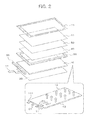
- FIG. 2 is a perspective view showing a configuration of the backlight 400 .
- a light source 20 with LEDs is disposed on a side surface of a light guide plate 10 .
- a flexible wiring substrate 27 for light sources is connected to the light source 20 .
- a reflecting sheet 30 for directing light toward the liquid crystal display panel is placed on a lower surface of the light guide plate 10 .
- a diffusing sheet 40 for diffusing the light uniformly is placed on the light guide plate 10 .
- a lower prismatic sheet 50 with a large number of linear prismatic structures formed in a specific direction on the sheet, is disposed on the diffusing sheet 40 .
- an upper prismatic sheet 60 is disposed on the lower prismatic sheet 50 .
- the lower prismatic sheet 50 and the upper prismatic sheet 60 perform the function of directing in a direction normal to the liquid crystal display panel 300 the light incident in an oblique direction relative to the liquid crystal display panel 300 , thereby raising the efficiency in the use of the light coming in from the backlight.
- a light-blocking sheet 70 for blocking out the light that may propagate to the periphery of the screen of the liquid crystal display panel is formed in a shape of a frame on the upper prismatic sheet 60 .
- the optical parts described above are accommodated in a resin molding 80 .
- FIG. 3 is a schematic plan view representing a problem associated with a display screen 500 of a liquid crystal display panel employed in a conventional example.
- a light source 20 with LEDs is disposed near a side surface of the display region on the liquid crystal display panel.
- This area is referred to as a yellowing area 510 .
- FIG. 4 is a perspective view of the light guide plate 10 .
- One side 11 of the light guide plate 10 functions as a plane of incidence, and an upper surface of the light guide plate 10 functions as an exit surface 12 .
- On the exit surface 12 such linear protrusions 121 as denoted by reference number 121 in FIG. 4 extend in an x-direction, and these protrusions are arrayed in a y-direction.
- the lower surface of the light guide plate 10 serves as a plane of reflection, on which such linear protrusions 131 as represented by a dotted line 131 in FIG. 4 extend in the y-direction, and these protrusions are arrayed in the x-direction.
- the thickness of the light guide plate 10 ranges, for example, from 0.3 to 0.5 mm.
- the light guide plate 10 is made from a transparent or translucent resin, such as acryl or polycarbonate.
- FIG. 5 is a cross-sectional view of section A-A shown in FIG. 4 .
- the LEDs 21 or the light source, that face the plane of incidence of the light guide plate 10 are disposed as represented by a dotted line.
- the linear protrusions 121 with height h 1 are formed at pitches p 1 on the upper surface of the light guide plate 10 .
- the length of each pitch p 1 is 100 ⁇ m, for example.
- the height of each linear protrusion 121 is smallest at the portion closest to the LEDs, and increases with longer distance from the LEDs.
- each linear protrusion 121 is, for example, 0.1 ⁇ m at the portion closest to the LEDs, and 10 ⁇ m at the portion farthest therefrom.
- Upper linear protrusions 121 have, for example, substantially the same triangular cross-sectional shape as that of a linear prism.
- FIG. 6 is a cross-sectional view of section B-B shown in FIG. 4 .
- lower linear protrusions 131 are formed at pitches p 2 and with height h 2 .
- the length of each pitch p 2 is 100 ⁇ m, for example, and the height h 2 is constant and is, for example, 10 ⁇ m.
- the lower linear protrusions 131 are, for example, arc-shaped or barrel-shaped in cross-sectional profile.
- FIG. 7 is a perspective view showing a shape of one of the LEDs 20 .
- Width w 1 of a light-emitting surface on the LED 20 is, for example, 3.0 mm, and package width w 3 of the LED 20 is, for example, 3.8 mm.
- An electrode 25 for supplying an electric current to an LED chip is formed on adjacent sides of the LED 21 .
- FIG. 7 shows a white LED, and this LED is designed to emit white light.
- a luminous spectrum developed on the light-emitting surface 24 is measured in detail along a dotted line shown in FIG. 7 , however, the spectrum of the LED 21 is mainly occupied by blue at around the central area of the LED, and is mainly occupied by yellow at adjacent sides of the central area.
- the area shown as B in FIG. 7 denotes the one where blue predominates, and that shown as Y denotes the one where yellow predominates.
- Width w 2 of the area where blue predominates is 1
- FIG. 8 is a CIE 1976 UCS chromaticity diagram. As shown in FIG. 8 , a horizontal axis denotes u′ and a vertical axis denotes v′. FIG. 8 shows that as v′ increases, the light assumes a more yellowish color, and that as v′ decreases, the light assumes a more bluish color.
- FIG. 9 is a representation of changes in the u′ value as measured along the dotted line across the light-emitting surface in FIG. 7
- FIG. 10 is a representation of changes in the v′ value as measured along the dotted line across on the light-emitting surface in FIG. 7 .
- u′ undergoes only minimal changes.
- v′ decreases in its horizontal data range of ⁇ 0.5 mm across the center of the light-emitting surface.
- This area corresponds to an area in which v′ is smaller than 0.4. In other words, in this area, blue is relatively predominant, compared to other areas of the light-emitting surface, and yellow is predominant at adjacent sides of the area.
- FIG. 11 is a cross-sectional view of the LED 21 , taken along a surface parallel to a principal plane of the light guide plate.
- the LED package in FIG. 11 contains the LED chip 22 that is surrounded with a yellow fluorescent substance 23 . Blue light emissions from the LED chip 22 are subject to color conversion by the fluorescent substance, thus becoming white light as a whole. When the light is microscopically viewed, however, its chromaticity slightly varies from location to location on the light-emitting surface.
- the light emitted directly to above the LED chip 22 that is, in a direction normal to the light-emitting surface, will assume a slightly bluish color rather than a white color, since the light will only be color-converted at a short distance by the yellow fluorescent substance 23 .
- the light emitted in a direction that forms an angle with the direction normal to the light-emitting surface will assume a slightly yellowish color rather than a white color, since the light will be color-converted at a long distance by yellow fluorescent substance 23 .
- FIG. 12 is a schematic plan view showing a path that such LED light as shown in FIG. 11 travels after entering the light guide plate 10 . Since the bluish light B that has been emitted in the direction normal to the light-emitting surface of the LED enters the plane of incidence of the light guide plate 10 vertically, the bluish light B travels straight ahead and goes a longer distance inside the light guide plate 10 . By contrast, the light emitted at a certain angle with respect to the direction normal to the light-emitting surface of the LED is most likely to stay in a greater amount near the light source after being reflected or scattered by the reflecting surface protrusions 131 or the like. In the area close to the light source, therefore, the light emitted from the light guide plate 10 is more yellowish than in other areas. This event is considered to cause yellowish color unevenness on the light source side of the screen in the conventional example.
- FIG. 13 is a perspective view that shows exemplary layout of a light guide plate 10 and LEDs 21 serving as a light source.
- the LEDs 21 in FIG. 13 are arranged at pitches p 3 in an x-direction along a plane of incidence 11 on the light guide plate 10 .
- the pitches p 3 range, for example, between 5 and 10 mm.
- Width w 3 of the LEDs 21 in the x-direction, corresponds to the width of the LED package shown in FIG. 7 .
- the width w 3 is, for example, 3.8 mm.
- Light that has entered the light guide plate 10 exits from an exit surface 12 and travels toward a liquid crystal display panel disposed above. By contrast, light heading downward from the light guide plate 10 is reflected by a reflecting sheet 30 and then directed toward the exit surface 12 .
- FIG. 14 is an enlarged plan view showing a positional relationship between the light guide plate 10 and LED 21 in the conventional example. While an ideal distance between the LED 21 and the light guide plate 10 is zero, there actually is a slight distance due to manufacturing variations in products.
- the LED configuration is as described in FIG. 11 .
- yellowish light due to the reflection or scattering inside the light guide plate 10 is present in a large amount near the LED, hence causing the yellowing of the screen.
- FIG. 15A is a plan view showing a positional relationship between an LED 21 and light guide plate 10 in the first embodiment of the present invention.
- the LED 21 has the same configuration as that described in FIG. 11 .
- LED 21 configurations in a second and subsequent embodiments of the present invention are also the same as the LED 21 configuration of FIG. 11 .
- incident plane protrusions 111 are formed on a plane of incidence of the light guide plate that corresponds to the area where a blue color predominates in the LED 21 . These protrusions are disposed to scatter bluish light.
- the protrusions 111 are provided in association with the area where v′ in FIG. 10 is smaller than 0.4. This means that if the LED 21 corresponding to FIG. 10 is used, the area where blue predominates will be formed in a horizontal data range of ⁇ 0.5 mm across the central area of the LED 21 .
- the width of the area where v′ in FIG. 10 is smaller than 0.4 may be expressed as w 2 . Even if the incident plane protrusions 111 are formed in an area narrower than w 2 , the liquid crystal display device according to the present embodiment will still be effective to a certain degree. In addition, while it has been described as per FIG. 10 that the bluish area is where v′ is smaller than or equal to 0.4, the value is not limited to 0.4.
- the liquid crystal display device according to the present embodiment will still be effective to a certain degree by forming incident plane protrusions 111 on the plane of incidence of the light guide plate 10 so as to make the incident plane protrusions 111 correspond to that part.
- FIG. 15B is an enlarged plan view showing a shape of the incident plane protrusions 111 on the plane of incidence of the light guide plate 10 in FIG. 15A .
- Height h 4 of the incident plane protrusions 111 in FIG. 15B is, for example, 5 ⁇ m
- pitch p 4 of the incident plane protrusions 111 is, for example, 20 ⁇ m.
- the incident plane protrusions 111 are, for example, arc-shaped or barrel-shaped in cross-sectional profile on a surface parallel to a principal plane of the light guide plate. Only four incident plane protrusions are formed in FIG. 15B . However, a larger number of protrusions, nearly 50 pieces for example, are formed in practice.
- FIG. 15C is a perspective view of the area in which the incident plane protrusions 111 on the plane of incidence 11 of the light guide plate 10 are formed.
- the incident plane protrusions 111 are formed linearly at the pitches p 4 over the entire thickness direction of the light guide plate 10 . While incident plane protrusions 111 in a second and subsequent embodiments of the present invention will only be described in plan view, these incident plane protrusions 111 are formed linearly over the entire thickness direction of a light guide plate 10 , as with the protrusions of FIG. 15C .
- the occurrence of yellowing near the light source can be mitigated since the incident plane protrusions 11 on the light guide plate 10 refract the bluish light that the LED 21 has emitted primarily from around the central area of the light-emitting surface.
- FIG. 16A is a plan view showing a positional relationship between an LED 21 and light guide plate 10 in the second embodiment of the present invention.
- the LED 21 has substantially the same configuration as that described in FIG. 11 .
- incident plane protrusions 111 are formed on the plane of incidence of the light guide plate that corresponds to the area where blue predominates in the LED 21 .
- the present embodiment differs from the first embodiment in that the incident plane protrusions 111 are prismatic or triangular in cross-sectional profile on a surface parallel to a principal plane of the light guide plate.
- Other configurational aspects are substantially the same as in FIG. 1 .
- FIG. 16B is an enlarged plan view showing a shape of the incident plane protrusions 111 formed on the plane of incidence 11 of the light guide plate 10 in FIG. 16A .
- Height h 4 of the incident plane protrusions 111 in FIG. 16B is, for example, 5 ⁇ m
- pitch p 4 of the incident plane protrusions 111 is, for example, 20 ⁇ m. That is to say, the height h 4 and the pitch p 4 are the same as in the first embodiment.
- the incident plane protrusions 111 are typically 90 degrees in apex angle ⁇ . This angle is set to be 90 degrees to obtain incident light refraction characteristics and for a reason of the ease of manufacturing of the incident plane protrusions, but the liquid crystal display device according to the present embodiment still offers the advantageous effects with other angles.
- the occurrence of yellowing near the light source can be mitigated since the incident plane protrusions 111 on the light guide plate 10 refract the bluish light that the LED 21 has been emitted primarily from around the central area of the light-emitting surface.
- FIG. 17A is a plan view showing a positional relationship between an LED 21 and light guide plate 10 in a third embodiment of the present invention.
- the LED 21 has substantially the same configuration as that described in FIG. 11 .
- incident plane protrusions 111 are formed in both the area where a blue color predominates and the area where a yellow color predominates.
- the incident plane protrusions 111 on the section corresponding to the area where blue predominates are formed at pitches shorter than those of the incident plane protrusions 111 formed on the section corresponding to the area where yellow predominates.
- the density of the incident plane protrusions 111 in the former of the two areas is higher than in the latter. This means that on the section where blue predominates, a greater amount of light is refracted and scattered than on other sections, so that there is a greater amount of blue in an area close to the light source.
- FIG. 17B is an enlarged plan view showing a shape of the incident plane protrusions 111 formed on the plane of incidence of the light guide plate 10 in FIG. 17A .
- the incident plane protrusions 111 on the section of the light guide plate 10 that corresponds to the LED area where blue predominates are formed at pitches p 5 are formed at pitches p 5 .
- p 5 ⁇ p 6 holds.
- the incident plane protrusions 111 are formed at a density higher than in other areas.
- the height of the incident plane protrusions 111 is shown as h 5 , which is the same for both the section where blue predominates and the section where yellow predominates.
- the values of p 5 , p 6 , and h 5 are, for example, 20 ⁇ m, 40 ⁇ m, and 5 ⁇ m, respectively.
- FIG. 17B only three incident plane protrusions 111 are formed in the LED area where blue predominates. However, a larger number of protrusions, nearly 50 pieces for example, are formed in practice.
- the incident plane protrusions 111 in FIGS. 17A and 17B are arc-shaped in cross-sectional profile, but the protrusions do not always need to have the shape of an arc. Instead, they may have such a prismatic shape that is shown in the second embodiment.
- the incident plane protrusions 111 on the section of the light guide plate 10 that corresponds to a specific area of the LED 21 are formed at a density higher than at any other sections.
- the bluish light emitted from an area close to the central area of the light-emitting surface is thus refracted or scattered in a greater amount, so that the occurrence of yellowing near the light source is mitigated.
- FIG. 18A is a plan view showing a positional relationship between an LED 21 and light guide plate 10 in a fourth embodiment of the present invention.
- the LED 21 has substantially the same configuration as that described in FIG. 11 .
- incident plane protrusions 111 are formed in both of the area where a blue color predominates and the area where a yellow color predominates.
- the height of the incident plane protrusions 111 on the section corresponding to the area where blue predominates in the LED 21 is greater than that of the incident plane protrusions 111 formed on the section corresponding to the area where yellow predominates in the LED 21 .
- Such a shape of the protrusions increases the refraction or scattering of the light on the section where blue predominates.
- FIG. 18B is an enlarged plan view showing a shape of the incident plane protrusions 111 formed on the plane of incidence of the light guide plate 10 in FIG. 18A .
- the incident plane protrusions 111 on the section of the light guide plate 10 that corresponds to the area where blue predominates in the LED 21 are formed at pitches p 7 and the incident plane protrusions 111 on the section of the light guide plate 10 that correspond to the area where yellow predominates in the LED 21 are also formed at the pitches p 7 .
- height h 7 of the incident plane protrusions 111 on the section of the light guide plate 10 that corresponds to the area where blue predominates in the LED 21 is greater than height h 8 of the incident plane protrusions 111 formed on the section of the light guide plate 10 that corresponds to the area where yellow predominates in the LED 21 .
- the pitches p 7 of the incident plane protrusions 111 are, for example, 20 ⁇ m
- the height h 7 is, for example, 3 ⁇ m
- the height h 8 is, for example, 1 ⁇ m.
- FIG. 18C is a cross-sectional comparative view of two incident plane protrusions 111 that differ in height. As shown in FIG. 18C , even if the two incident plane protrusions 111 have the same width, the one that is greater in height tends to be smaller in a radius of curvature of the incident plane protrusion, so that this protrusion refracts or scatters incident light in a greater amount.
- the height of the incident plane protrusions 111 formed on the section of the light guide plate 10 that corresponds to a specific area in the LED 21 is greater than the height of other sections, the bluish light emitted from an area close to a central area of the light-emitting surface on the LED 21 will be refracted or scattered in a greater amount, so that the occurrence of yellowing near the light source is mitigated.
- FIG. 19 is a plan view showing a section of a light guide plate 10 that corresponds to a light-emitting surface of an LED 21 in a fifth embodiment of the present invention.
- the present embodiment has a configuration that incorporates features of both the third and fourth embodiments.
- incident plane protrusions 111 are formed in both of the area where a yellow color predominates and the area where a blue color predominates.
- the incident plane protrusions 111 on the section corresponding to the LED area where blue predominates are greater in height and shorter in pitch than the incident plane protrusions 111 on the section corresponding to the LED area where yellow predominates.
- Height h 7 of the incident plane protrusions 111 on the section corresponding to the LED area where blue predominates is, for example, 3 ⁇ m
- pitch p 7 is, for example, 20 ⁇ m.
- Height h 8 of the incident plane protrusions 111 on the section corresponding to the LED area where yellow predominates is, for example, 1 ⁇ m
- pitch p 8 is, for example, 40 ⁇ m.
- the height of the incident plane protrusions 111 formed on the section of the light guide plate 10 that corresponds to a specific area in the LED 21 is greater than that of other sections, and the pitch of these incident plane protrusions is shorter than that of the other sections. Accordingly the bluish light emitted from around the central area of the light-emitting surface on the LED 21 is refracted or scattered in a greater amount, so that the occurrence of yellowing near the light source is mitigated.
- FIG. 20A is a plan view showing a positional relationship between an LED 21 and light guide plate 10 in a sixth embodiment of the present invention.
- the LED 21 has substantially the same configuration as that described in FIG. 11 .
- incident plane protrusions 111 are formed in both of the area where a blue color predominates and the area where a yellow color predominates. While the height of the incident plane protrusions 111 is greater at the section corresponding to the area where blue predominates in the LED 21 , the height of these incident plane protrusions 111 progressively diminishes with decreasing distance with respect to the area where yellow predominates.
- the pitches of the incident plane protrusions 111 are the same for both the area where blue predominates and the area where yellow predominates.
- FIG. 20B is an enlarged plan view of the light guide plate 10 with the sections corresponding to a light-emitting area of the LED 21 , the plan view showing an exemplary layout of the above two sets of incident plane protrusions.
- the height of the incident plane protrusions 111 in the area where blue predominates is shown as h 10 the height of the incident plane protrusions 111 in the area where yellow predominates is shown as h 12
- the height of other incident plane protrusions 111 present in between the former two sets of incident plane protrusions 111 is shown as h 11 .
- the height h 11 is of the incident plane protrusions 111 present at a boundary of the area where blue predominates and the area where yellow predominates.
- the pitch of the incident plane protrusions 111 in FIG. 20B is constant, which is 20 ⁇ m, for example.
- the height h 10 of the incident plane protrusions 111 is 3 ⁇ m, the height h 11 is 2 ⁇ m, and the height h 12 is 1 ⁇ m, for example.
- the height h 10 of the incident plane protrusions 111 is constant at the area where blue predominates, and progressively diminishes to a level of h 12 at the area where yellow predominates.
- the height of the incident plane protrusions may be set as the greatest height h 10 of the three heights, and may also progressively diminish to the level of h 12 at an outer edge of the area where yellow predominates. In this way, the height of the protrusions may be continuously changed.
- the occurrence of yellowing near the light source can be mitigated since at the plane of incidence 11 of the light guide plate 10 , bluish light that the LED 21 emits is refracted or scattered in a greater amount than yellowish light.
- incident plane protrusions in the fourth to sixth embodiments are arc-shaped in cross-sectional profile, the shape of the incident plane protrusions may be triangular or prismatic, as in the second embodiment.
Abstract
This invention reduces or prevents a phenomenon where a screen close to a light source becomes yellowed. A liquid crystal display device includes a liquid crystal display panel and a backlight. The backlight includes a light guide plate 10 and white LEDs 21 arrayed in a first direction on a plane of incidence 11 of the light guide plate 10. The white LEDs 21 each includes, in the first direction on a light-emitting surface, a central area occupied by a blue spectrum more densely than at adjacent sides of the central area. Incident plane protrusions 111, each extending in a thickness direction of the light guide plate 10, are formed on a section corresponding to the area having the dense blue spectrum of each LED 21, at the plane of incidence 11 of the light guide plate 10.
Description
The present application claims priority from Japanese Patent Application JP 2014-217462 filed on Oct. 24, 2014, the content of which is hereby incorporated by reference into this application.
1. Field of the Invention
The present invention relates to liquid crystal display devices that each includes a backlight using light-emitting diodes (LEDs) as a light source, the liquid crystal display devices incorporating a preventive measure against color unevenness in the vicinity of the light source.
2. Description of the Related Art
Liquid crystal display devices include a thin-film transistor (TFT) substrate formed by elements such as pixel electrodes and TFTs, a counter substrate facing the TFT substrate, and liquid crystals sandwiched between the TFT substrate and the counter substrate. The transmittance of the light passing through the liquid crystal molecules is controlled on a pixel-by-pixel basis to form an image.
Since the liquid crystals themselves do not emit light, a backlight is disposed on a rear side of a liquid crystal display panel. Each of the liquid crystal display devices such as cellular phones uses LEDs as a light source for the backlight. The LEDs are arranged on a side surface of a light guide plate, various optical sheets are also arranged on the light guide plate, and these optical parts are accommodated in a molding, thereby to configure the backlight. The method of arranging the LEDs on the side surface of the light guide plate is called the side light method.
The LEDs constitute a point light source, and the uniformity of luminance in the backlight therefore is a vital factor. JP-A-2013-69498 describes a configuration intended to obtain uniform luminance of a backlight by forming linear prismatic grooves on a lower surface of a light guide plate. JP-A-2013-93199 describes configurations of two kinds of grooved structures. One of the grooves structures is disposed on at least one of a light-emitting surface and a counter surface of a light guide plate. The other one having anisotropic diffusion characteristics is on the light-receiving surface. These grooved structures enable uniform luminance of light from a backlight.
The configurations described in JP-A-2013-69498 and JP-A-2013-93199 both intend to improve the uniformity of luminance in the respective backlights that use white LEDs. White LEDs are commonly used to obtain white light by placing a yellow fluorescent substance around an LED chip configured to emit high-energy light. In each backlight using these LEDs, when a white color is displayed, an area in which the white color has shifted to yellow tends to occur in an area relatively close to the light source. The present invention is intended to prevent this problem, that is, yellowing, from occurring.
An object of the present invention is to overcome the above problem, specifically by the following methods.
(1) A liquid crystal display device including a liquid crystal display panel and a backlight. The backlight includes a light guide plate and white LEDs arrayed in a first direction on a plane of incidence of the light guide plate. The white LEDs each includes, in the first direction on a light-emitting surface, a central area occupied by a blue spectrum more densely than at its both sides. Incident plane protrusions, each extending in a thickness direction of the light guide plate, are formed on a section corresponding to the area having the dense blue spectrum of the LEDs at the plane of incidence of the light guide plate.
(2) The liquid crystal display device described in above item (1), wherein an amount of light, refracted on the section corresponding to the area having the dense blue spectrum of the LEDs at the plane of incidence of the light guide plate, is larger than an amount of light refracted in any other areas of the light guide plate.
(3) The liquid crystal display device described in above item (1), wherein the area having the dense blue spectrum has a maximum “u′” value of 0.4 on a CIE chromaticity diagram′
(4) A liquid crystal display device including a liquid crystal display panel and a backlight, the backlight including a light guide plate and white LEDs arrayed in a first direction on a plane of incidence of the light guide plate. The white LEDs each includes on a light-emitting surface: a first area occupied by a blue spectrum more densely than at adjacent sides of the first area in the center of the first direction on the light-emitting surface; and a second area occupied by a yellow spectrum more densely than at adjacent sides of the second area in the first direction on the light-emitting surface than in the first area. First incident plane protrusions, each extending in a thickness direction of the light guide plate, are formed on a section corresponding to the first area of each LED, at the plane of incidence of the light guide plate; and second incident plane protrusions, each extending in the thickness direction of the light guide plate, are formed on a section corresponding to the second area of the LED at the plane of incidence of the light guide plate. The first incident plane protrusions are formed at pitches shorter than those of the second incident plane protrusions.
(5) The liquid crystal display device described in above item (4), wherein the height of the first incident plane protrusions is greater than that of the second incident plane protrusions.
(6) A liquid crystal display device including a liquid crystal display panel and a backlight, the backlight including a light guide plate and white LEDs arrayed in a first direction on a plane of incidence of the light guide plate. The white LEDs each includes on a light-emitting surface: a first area occupied by a blue spectrum more densely than at adjacent sides of the first area in the center of the first direction on the light-emitting surface; and a second area occupied by a yellow spectrum more densely than at adjacent sides of the second area in the first direction on the light-emitting surface than in the first area. First incident plane protrusions, each extending in a thickness direction of the light guide plate, are formed on a section corresponding to the first area of each LED at the plane of incidence of the light guide plate; and second incident plane protrusions, each extending in the thickness direction of the light guide plate, are formed on a section corresponding to the second area of the LED at the plane of incidence of the light guide plate. The height of the first incident plane protrusions is greater than that of the second incident plane protrusions.
(7) The liquid crystal display device described in above item (6), wherein a pitch of the first incident plane protrusions is the same as that of the second incident plane protrusions.
(8) The liquid crystal display device described in any one of items (4) to (7), wherein the area having the dense blue spectrum has a maximum “u′” value of 0.4 on a CIE chromaticity diagram.
(9) The liquid crystal display device described in any one of items (1) to (8), wherein the incident plane protrusions are arc-shaped in cross-sectional profile on a surface parallel to a principal plane of the light guide plate.
(10) The liquid crystal display device described in any one of items (1) to (8), wherein the incident plane protrusions are triangular in cross-sectional profile on a surface parallel to a principal plane of the light guide plate.
The present invention will be described in detail below with reference to embodiments thereof.
This color distribution is considered to be due to such a configuration of the LED 21 that is shown in FIG. 11 . FIG. 11 is a cross-sectional view of the LED 21, taken along a surface parallel to a principal plane of the light guide plate. The LED package in FIG. 11 contains the LED chip 22 that is surrounded with a yellow fluorescent substance 23. Blue light emissions from the LED chip 22 are subject to color conversion by the fluorescent substance, thus becoming white light as a whole. When the light is microscopically viewed, however, its chromaticity slightly varies from location to location on the light-emitting surface.
Referring to FIG. 11 , the light emitted directly to above the LED chip 22, that is, in a direction normal to the light-emitting surface, will assume a slightly bluish color rather than a white color, since the light will only be color-converted at a short distance by the yellow fluorescent substance 23. The light emitted in a direction that forms an angle with the direction normal to the light-emitting surface will assume a slightly yellowish color rather than a white color, since the light will be color-converted at a long distance by yellow fluorescent substance 23.
The width of the area where v′ in FIG. 10 is smaller than 0.4 may be expressed as w2. Even if the incident plane protrusions 111 are formed in an area narrower than w2, the liquid crystal display device according to the present embodiment will still be effective to a certain degree. In addition, while it has been described as per FIG. 10 that the bluish area is where v′ is smaller than or equal to 0.4, the value is not limited to 0.4. If part of the central area is smaller in magnitude of the v′ value than on adjacent sides of the central area, the liquid crystal display device according to the present embodiment will still be effective to a certain degree by forming incident plane protrusions 111 on the plane of incidence of the light guide plate 10 so as to make the incident plane protrusions 111 correspond to that part.
As set forth above, in accordance with the present embodiment, the occurrence of yellowing near the light source can be mitigated since the incident plane protrusions 11 on the light guide plate 10 refract the bluish light that the LED 21 has emitted primarily from around the central area of the light-emitting surface.
As set forth above, in accordance with the present embodiment, the occurrence of yellowing near the light source can be mitigated since the incident plane protrusions 111 on the light guide plate 10 refract the bluish light that the LED 21 has been emitted primarily from around the central area of the light-emitting surface.
Referring to FIG. 17B , only three incident plane protrusions 111 are formed in the LED area where blue predominates. However, a larger number of protrusions, nearly 50 pieces for example, are formed in practice. The incident plane protrusions 111 in FIGS. 17A and 17B are arc-shaped in cross-sectional profile, but the protrusions do not always need to have the shape of an arc. Instead, they may have such a prismatic shape that is shown in the second embodiment.
As set forth above, in accordance with the third embodiment, the incident plane protrusions 111 on the section of the light guide plate 10 that corresponds to a specific area of the LED 21 are formed at a density higher than at any other sections. The bluish light emitted from an area close to the central area of the light-emitting surface is thus refracted or scattered in a greater amount, so that the occurrence of yellowing near the light source is mitigated.
As set forth above, in accordance with the present embodiment, since the height of the incident plane protrusions 111 formed on the section of the light guide plate 10 that corresponds to a specific area in the LED 21 is greater than the height of other sections, the bluish light emitted from an area close to a central area of the light-emitting surface on the LED 21 will be refracted or scattered in a greater amount, so that the occurrence of yellowing near the light source is mitigated.
As set forth above, in accordance with the present embodiment, the height of the incident plane protrusions 111 formed on the section of the light guide plate 10 that corresponds to a specific area in the LED 21 is greater than that of other sections, and the pitch of these incident plane protrusions is shorter than that of the other sections. Accordingly the bluish light emitted from around the central area of the light-emitting surface on the LED 21 is refracted or scattered in a greater amount, so that the occurrence of yellowing near the light source is mitigated.
Referring to FIG. 20A , the height h10 of the incident plane protrusions 111 is constant at the area where blue predominates, and progressively diminishes to a level of h12 at the area where yellow predominates. In the central area where blue predominates, however, the height of the incident plane protrusions may be set as the greatest height h10 of the three heights, and may also progressively diminish to the level of h12 at an outer edge of the area where yellow predominates. In this way, the height of the protrusions may be continuously changed.
As set forth above, in accordance with the present embodiment, the occurrence of yellowing near the light source can be mitigated since at the plane of incidence 11 of the light guide plate 10, bluish light that the LED 21 emits is refracted or scattered in a greater amount than yellowish light.
While the incident plane protrusions in the fourth to sixth embodiments are arc-shaped in cross-sectional profile, the shape of the incident plane protrusions may be triangular or prismatic, as in the second embodiment.
Claims (17)
1. A liquid crystal display device comprising:
a liquid crystal display panel; and
a backlight,
the backlight including a light guide plate and white LEDs arrayed in a first direction and opposed to a plane of incidence of the light guide plate,
the white LEDs each including, in the first direction on a light-emitting surface, a central area occupied by a blue spectrum more densely than at its both sides,
wherein incident plane protrusions, extending in a direction that is perpendicular to a thickness direction of the light guide plate, are formed on a first section corresponding to the area having the dense blue spectrum of the LEDs at the plane of incidence of the light guide plate and a second section corresponding to both sides of the central area, and
a pitch of incident plane protrusions formed on the first section is shorter than that of incident plane protrusions formed on the second section.
2. The liquid crystal display device according to claim 1 , wherein an amount of light, refracted on the section corresponding to the area having the dense blue spectrum of the LEDs at the plane of incidence of the light guide plate, is larger than an amount of light refracted in any other areas of the light guide plate.
3. The liquid crystal display device according to claim 1 , wherein the area having the dense blue spectrum has a maximum “u′” value of 0.4 on a CIE chromaticity diagram.
4. The liquid crystal display device according to claim 1 , wherein the incident plane protrusions are arc-shaped in cross-sectional profile on a surface parallel to a principal plane of the light guide plate.
5. The liquid crystal display device according to claim 1 , wherein the incident plane protrusions are triangular in cross-sectional profile on a surface parallel to a principal plane of the light guide plate.
6. A liquid crystal display device comprising:
a liquid crystal display panel; and
a backlight,
the backlight including a light guide plate and white LEDs arrayed in a first direction and opposed to a plane of incidence of the light guide plate,
the white LEDs each including on a light-emitting surface:
a first area occupied by a blue spectrum more densely than at adjacent sides of the first area in the center of the first direction on the light-emitting surface; and
a second area occupied by a yellow spectrum more densely at adjacent sides of the second area in the first direction on the light-emitting surface than in the first area, wherein
first incident plane protrusions, extending in a direction that is perpendicular to a thickness direction of the light guide plate, are formed on a section corresponding to the first area of each LED, at the plane of incidence of the light guide plate,
second incident plane protrusions, extending in the direction that is perpendicular to the thickness direction of the light guide plate, are formed on a section corresponding to the second area of the LED, at the plane of incidence of the light guide plate, and
the first incident plane protrusions are formed at pitches shorter than those of the second incident plane protrusions.
7. The liquid crystal display device according to claim 6 , wherein the height of the first incident plane protrusions is greater than that of the second incident plane protrusions.
8. The liquid crystal display device according to claim 7 , wherein the area having the dense blue spectrum has a maximum “u′” value of 0.4 on a CIE chromaticity diagram.
9. The liquid crystal display device according to claim 6 , wherein the area having the dense blue spectrum has a maximum “u′” value of 0.4 on a CIE chromaticity diagram.
10. The liquid crystal display device according to claim 6 , wherein the incident plane protrusions are arc-shaped in cross-sectional profile on a surface parallel to a principal plane of the light guide plate.
11. The liquid crystal display device according to claim 6 wherein the incident plane protrusions are triangular in cross-sectional profile on a surface parallel to a principal plane of the light guide plate.
12. A liquid crystal display device comprising:
a liquid crystal display panel; and
a backlight,
the backlight including a light guide plate and white LEDs arrayed in a first direction and opposed to a plane of incidence of the light guide plate,
the white LEDs each including on a light-emitting surface:
a first area occupied by a blue spectrum more densely than at adjacent sides of the first area in the center of the first direction on the light-emitting surface; and
a second area occupied by a yellow spectrum more densely at adjacent sides of the second area in the first direction on the light-emitting surface than in the first area, wherein
first incident plane protrusions, extending in a direction that is perpendicular to a thickness direction of the light guide plate, are formed on a section corresponding to the first area of each LED, at the plane of incidence of the light guide plate,
second incident plane protrusions, extending in the direction that is perpendicular to the thickness direction—of the light guide plate, are formed on a section corresponding to the second area of the LED, at the plane of incidence of the light guide plate, and
the height of the first incident plane protrusions is greater than that of the second incident plane protrusions.
13. The liquid crystal display device according to claim 12 , wherein a pitch of the first incident plane protrusions is the same as that of the second incident plane protrusions.
14. The liquid crystal display device according to claim 13 , wherein the area having the dense blue spectrum has a maximum “u′” value of 0.4 on a CIE chromaticity diagram.
15. The liquid crystal display device according to claim 12 , wherein the area having the dense blue spectrum has a maximum “u′” value of 0.4 on a CIE chromaticity diagram.
16. The liquid crystal display device according to claim 12 , wherein the incident plane protrusions are arc-shaped in cross-sectional profile on a surface parallel to a principal plane of the light guide plate.
17. The liquid crystal display device according to claim 12 , wherein the incident plane protrusions are triangular in cross-sectional profile on a surface parallel to a principal plane of the light guide plate.
Priority Applications (1)
| Application Number | Priority Date | Filing Date | Title |
|---|---|---|---|
| US15/854,069 US10578922B2 (en) | 2014-10-24 | 2017-12-26 | Liquid crystal display device |
Applications Claiming Priority (2)
| Application Number | Priority Date | Filing Date | Title |
|---|---|---|---|
| JP2014-217462 | 2014-10-24 | ||
| JP2014217462A JP6585892B2 (en) | 2014-10-24 | 2014-10-24 | Liquid crystal display |
Related Child Applications (1)
| Application Number | Title | Priority Date | Filing Date |
|---|---|---|---|
| US15/854,069 Continuation US10578922B2 (en) | 2014-10-24 | 2017-12-26 | Liquid crystal display device |
Publications (2)
| Publication Number | Publication Date |
|---|---|
| US20160116667A1 US20160116667A1 (en) | 2016-04-28 |
| US9885913B2 true US9885913B2 (en) | 2018-02-06 |
Family
ID=55791853
Family Applications (2)
| Application Number | Title | Priority Date | Filing Date |
|---|---|---|---|
| US14/920,632 Active 2036-02-08 US9885913B2 (en) | 2014-10-24 | 2015-10-22 | Liquid crystal display device |
| US15/854,069 Active 2035-12-26 US10578922B2 (en) | 2014-10-24 | 2017-12-26 | Liquid crystal display device |
Family Applications After (1)
| Application Number | Title | Priority Date | Filing Date |
|---|---|---|---|
| US15/854,069 Active 2035-12-26 US10578922B2 (en) | 2014-10-24 | 2017-12-26 | Liquid crystal display device |
Country Status (2)
| Country | Link |
|---|---|
| US (2) | US9885913B2 (en) |
| JP (1) | JP6585892B2 (en) |
Cited By (1)
| Publication number | Priority date | Publication date | Assignee | Title |
|---|---|---|---|---|
| US20180120645A1 (en) * | 2014-10-24 | 2018-05-03 | Japan Display Inc. | Liquid crystal display device |
Families Citing this family (4)
| Publication number | Priority date | Publication date | Assignee | Title |
|---|---|---|---|---|
| US9921356B2 (en) * | 2015-09-23 | 2018-03-20 | Apple Inc. | Display Backlight with Light Mixing Structures |
| CN107390434A (en) * | 2017-09-19 | 2017-11-24 | 京东方科技集团股份有限公司 | Backlight module and its assemble method and display panel |
| JP6498258B1 (en) * | 2017-11-17 | 2019-04-10 | ミネベアミツミ株式会社 | Surface lighting device |
| CN109616024B (en) * | 2018-10-31 | 2020-12-08 | 武汉华星光电技术有限公司 | Surface light source and display device using the same |
Citations (7)
| Publication number | Priority date | Publication date | Assignee | Title |
|---|---|---|---|---|
| US20100172155A1 (en) * | 2005-10-20 | 2010-07-08 | Samsung Electronics Co., Ltd. | Light guide unit for point light source, backlight assembly having the light guide unit and display device having the same |
| US20120050149A1 (en) * | 2010-08-25 | 2012-03-01 | Samsung Mobile Display Co., Ltd. | Backlight Unit and Liquid Crystal Display Including the Same |
| US20130033893A1 (en) * | 2011-08-03 | 2013-02-07 | Japan Display East Inc. | Display device |
| US20130070477A1 (en) | 2011-09-21 | 2013-03-21 | Minebea Co., Ltd. | Spread illuminating apparatus |
| JP2013093199A (en) | 2011-10-04 | 2013-05-16 | Asahi Kasei Corp | Light guide plate, plane light source device, and display device |
| US8449163B2 (en) * | 2009-09-15 | 2013-05-28 | Young Lighting Technology Inc. | Backlight module |
| US20130208502A1 (en) * | 2012-02-09 | 2013-08-15 | Minebea Co., Ltd. | Spread illuminating apparatus |
Family Cites Families (7)
| Publication number | Priority date | Publication date | Assignee | Title |
|---|---|---|---|---|
| JP4122738B2 (en) * | 2001-07-26 | 2008-07-23 | 松下電工株式会社 | Method for manufacturing light emitting device |
| JP5176273B2 (en) * | 2005-12-28 | 2013-04-03 | 日亜化学工業株式会社 | Light emitting device and manufacturing method thereof |
| JP2011014520A (en) * | 2008-12-04 | 2011-01-20 | Seiko Instruments Inc | Lighting device and display |
| JP2012155999A (en) * | 2011-01-26 | 2012-08-16 | Jvc Kenwood Corp | Lighting system and image display device |
| JP2013101892A (en) * | 2011-11-10 | 2013-05-23 | Minebea Co Ltd | Plane surface lighting device |
| US9170364B2 (en) * | 2012-12-05 | 2015-10-27 | Rambus Delaware Llc | Lighting assembly with a light guide having light-redirecting edge features |
| JP6585892B2 (en) * | 2014-10-24 | 2019-10-02 | 株式会社ジャパンディスプレイ | Liquid crystal display |
-
2014
- 2014-10-24 JP JP2014217462A patent/JP6585892B2/en active Active
-
2015
- 2015-10-22 US US14/920,632 patent/US9885913B2/en active Active
-
2017
- 2017-12-26 US US15/854,069 patent/US10578922B2/en active Active
Patent Citations (8)
| Publication number | Priority date | Publication date | Assignee | Title |
|---|---|---|---|---|
| US20100172155A1 (en) * | 2005-10-20 | 2010-07-08 | Samsung Electronics Co., Ltd. | Light guide unit for point light source, backlight assembly having the light guide unit and display device having the same |
| US8449163B2 (en) * | 2009-09-15 | 2013-05-28 | Young Lighting Technology Inc. | Backlight module |
| US20120050149A1 (en) * | 2010-08-25 | 2012-03-01 | Samsung Mobile Display Co., Ltd. | Backlight Unit and Liquid Crystal Display Including the Same |
| US20130033893A1 (en) * | 2011-08-03 | 2013-02-07 | Japan Display East Inc. | Display device |
| US20130070477A1 (en) | 2011-09-21 | 2013-03-21 | Minebea Co., Ltd. | Spread illuminating apparatus |
| JP2013069498A (en) | 2011-09-21 | 2013-04-18 | Minebea Co Ltd | Planar lighting device |
| JP2013093199A (en) | 2011-10-04 | 2013-05-16 | Asahi Kasei Corp | Light guide plate, plane light source device, and display device |
| US20130208502A1 (en) * | 2012-02-09 | 2013-08-15 | Minebea Co., Ltd. | Spread illuminating apparatus |
Cited By (2)
| Publication number | Priority date | Publication date | Assignee | Title |
|---|---|---|---|---|
| US20180120645A1 (en) * | 2014-10-24 | 2018-05-03 | Japan Display Inc. | Liquid crystal display device |
| US10578922B2 (en) * | 2014-10-24 | 2020-03-03 | Japan Display Inc. | Liquid crystal display device |
Also Published As
| Publication number | Publication date |
|---|---|
| US10578922B2 (en) | 2020-03-03 |
| US20160116667A1 (en) | 2016-04-28 |
| US20180120645A1 (en) | 2018-05-03 |
| JP6585892B2 (en) | 2019-10-02 |
| JP2016085329A (en) | 2016-05-19 |
Similar Documents
| Publication | Publication Date | Title |
|---|---|---|
| US10578922B2 (en) | Liquid crystal display device | |
| EP2808730B1 (en) | Display apparatus with a direct backlight | |
| US20170363798A1 (en) | Lighting device and display device | |
| US8692464B2 (en) | Light guiding plate, backlight module and display device | |
| US20130088857A1 (en) | Optical assembly, backlight unit having the same, and display apparatus thereof | |
| US9053650B2 (en) | Backlight unit and display apparatus thereof | |
| US20110164404A1 (en) | Illumination device, surface light source device, and liquid crystal display apparatus | |
| US9303845B2 (en) | Display apparatus | |
| TWI459089B (en) | Light guide plate and backlight module having the same | |
| US10534126B2 (en) | Lighting device and display device | |
| US20160161086A1 (en) | Light emitting module and light emitting apparatus | |
| JP5985364B2 (en) | Light source unit and lighting device | |
| US20130141897A1 (en) | LCD Device And LED Package Structure Thereof | |
| US10551549B2 (en) | Condensing sheet, backlight unit and liquid crystal display device using the same | |
| TWI670532B (en) | Back-light module | |
| WO2012147646A1 (en) | Light source device, surface light source device, display device, and illumination device | |
| US9400348B2 (en) | Display backlight unit having reflecting structure for reducing hotspots | |
| KR102232058B1 (en) | backlight unit and liquid crystal display module including the same | |
| KR101234841B1 (en) | Prism sheet having lengthwise wave patterned optical condensing portions and reflection portions, back light unit having the prism sheet and liquid crystal display device having the back light unit | |
| JP2008311091A (en) | Lighting system and display device using the same | |
| KR20110051390A (en) | Light emitting diode package, backlight unit and liquid crystal display having the same | |
| KR102081114B1 (en) | Condensing sheet, backlight unit and liquid crystal display device using the same | |
| KR101307715B1 (en) | Member for controlling luminous flux, light emitting device and display device | |
| KR20130071752A (en) | Reflector plate and backlight unit including the plate | |
| KR20140108056A (en) | Back Light Unit And Liquid Crystal Display Device Comprising The Same |
Legal Events
| Date | Code | Title | Description |
|---|---|---|---|
| AS | Assignment |
Owner name: JAPAN DISPLAY INC., JAPAN Free format text: ASSIGNMENT OF ASSIGNORS INTEREST;ASSIGNORS:SHIRAISHI, YASUHISA;ONISHI, TOMOHISA;REEL/FRAME:036860/0723 Effective date: 20150918 |
|
| STCF | Information on status: patent grant |
Free format text: PATENTED CASE |
|
| MAFP | Maintenance fee payment |
Free format text: PAYMENT OF MAINTENANCE FEE, 4TH YEAR, LARGE ENTITY (ORIGINAL EVENT CODE: M1551); ENTITY STATUS OF PATENT OWNER: LARGE ENTITY Year of fee payment: 4 |