US9882484B2 - Switching power supply device having pulse-by-pulse type overcurrent protection function - Google Patents
Switching power supply device having pulse-by-pulse type overcurrent protection function Download PDFInfo
- Publication number
- US9882484B2 US9882484B2 US15/381,353 US201615381353A US9882484B2 US 9882484 B2 US9882484 B2 US 9882484B2 US 201615381353 A US201615381353 A US 201615381353A US 9882484 B2 US9882484 B2 US 9882484B2
- Authority
- US
- United States
- Prior art keywords
- signal
- voltage
- overcurrent protection
- mask
- output
- Prior art date
- Legal status (The legal status is an assumption and is not a legal conclusion. Google has not performed a legal analysis and makes no representation as to the accuracy of the status listed.)
- Active
Links
Images


Classifications
-
- H—ELECTRICITY
- H02—GENERATION; CONVERSION OR DISTRIBUTION OF ELECTRIC POWER
- H02M—APPARATUS FOR CONVERSION BETWEEN AC AND AC, BETWEEN AC AND DC, OR BETWEEN DC AND DC, AND FOR USE WITH MAINS OR SIMILAR POWER SUPPLY SYSTEMS; CONVERSION OF DC OR AC INPUT POWER INTO SURGE OUTPUT POWER; CONTROL OR REGULATION THEREOF
- H02M3/00—Conversion of dc power input into dc power output
- H02M3/02—Conversion of dc power input into dc power output without intermediate conversion into ac
- H02M3/04—Conversion of dc power input into dc power output without intermediate conversion into ac by static converters
- H02M3/10—Conversion of dc power input into dc power output without intermediate conversion into ac by static converters using discharge tubes with control electrode or semiconductor devices with control electrode
- H02M3/145—Conversion of dc power input into dc power output without intermediate conversion into ac by static converters using discharge tubes with control electrode or semiconductor devices with control electrode using devices of a triode or transistor type requiring continuous application of a control signal
- H02M3/155—Conversion of dc power input into dc power output without intermediate conversion into ac by static converters using discharge tubes with control electrode or semiconductor devices with control electrode using devices of a triode or transistor type requiring continuous application of a control signal using semiconductor devices only
- H02M3/156—Conversion of dc power input into dc power output without intermediate conversion into ac by static converters using discharge tubes with control electrode or semiconductor devices with control electrode using devices of a triode or transistor type requiring continuous application of a control signal using semiconductor devices only with automatic control of output voltage or current, e.g. switching regulators
- H02M3/158—Conversion of dc power input into dc power output without intermediate conversion into ac by static converters using discharge tubes with control electrode or semiconductor devices with control electrode using devices of a triode or transistor type requiring continuous application of a control signal using semiconductor devices only with automatic control of output voltage or current, e.g. switching regulators including plural semiconductor devices as final control devices for a single load
-
- H—ELECTRICITY
- H02—GENERATION; CONVERSION OR DISTRIBUTION OF ELECTRIC POWER
- H02M—APPARATUS FOR CONVERSION BETWEEN AC AND AC, BETWEEN AC AND DC, OR BETWEEN DC AND DC, AND FOR USE WITH MAINS OR SIMILAR POWER SUPPLY SYSTEMS; CONVERSION OF DC OR AC INPUT POWER INTO SURGE OUTPUT POWER; CONTROL OR REGULATION THEREOF
- H02M1/00—Details of apparatus for conversion
- H02M1/08—Circuits specially adapted for the generation of control voltages for semiconductor devices incorporated in static converters
-
- H—ELECTRICITY
- H02—GENERATION; CONVERSION OR DISTRIBUTION OF ELECTRIC POWER
- H02M—APPARATUS FOR CONVERSION BETWEEN AC AND AC, BETWEEN AC AND DC, OR BETWEEN DC AND DC, AND FOR USE WITH MAINS OR SIMILAR POWER SUPPLY SYSTEMS; CONVERSION OF DC OR AC INPUT POWER INTO SURGE OUTPUT POWER; CONTROL OR REGULATION THEREOF
- H02M1/00—Details of apparatus for conversion
- H02M1/32—Means for protecting converters other than automatic disconnection
-
- H—ELECTRICITY
- H03—ELECTRONIC CIRCUITRY
- H03K—PULSE TECHNIQUE
- H03K17/00—Electronic switching or gating, i.e. not by contact-making and –breaking
- H03K17/08—Modifications for protecting switching circuit against overcurrent or overvoltage
-
- H—ELECTRICITY
- H02—GENERATION; CONVERSION OR DISTRIBUTION OF ELECTRIC POWER
- H02M—APPARATUS FOR CONVERSION BETWEEN AC AND AC, BETWEEN AC AND DC, OR BETWEEN DC AND DC, AND FOR USE WITH MAINS OR SIMILAR POWER SUPPLY SYSTEMS; CONVERSION OF DC OR AC INPUT POWER INTO SURGE OUTPUT POWER; CONTROL OR REGULATION THEREOF
- H02M1/00—Details of apparatus for conversion
- H02M1/0003—Details of control, feedback or regulation circuits
- H02M1/0009—Devices or circuits for detecting current in a converter
-
- H02M2001/0003—
-
- H02M2001/0009—
Definitions
- the present disclosure relates to a switching power supply device.
- a typically used type of the overcurrent protection circuit is a pulse-by-pulse type in which a forcible-stop and self-return of a switching operation is repeated at every period.
- the present disclosure provides some embodiments of a switching power supply device capable of enhancing a pulse-by-pulse type overcurrent protection function.
- a switching power supply device including: a switching output circuit configured to generate an output voltage from an input voltage; an oscillation circuit configured to generate a clock signal; a control circuit configured to control driving of the switching output circuit in synchronization with the clock signal; a pulse-by-pulse type overcurrent protection circuit configured to detect an overcurrent flowing through the switching output circuit to generate an overcurrent protection signal for forcibly stopping a switching operation of the switching output circuit; and a pulse skip circuit configured to perform a pulse skip operation of the clock signal in response to the overcurrent protection signal (first configuration).
- the pulse skip circuit may include: a frequency dividing part configured to start a frequency dividing operation of the clock signal in response to the overcurrent protection signal to generate a mask period expiration signal; an RS flipflop configured to generate a mask signal set to a first logic level in response to the overcurrent protection signal and reset to a second logic level in response to the mask period expiration signal; and a logic gate configured to block the clock signal over a mask period during which the mask signal is set to the first logic level (second configuration).
- the pulse skip circuit may include: a timer part configured to start a counting operation in response to the overcurrent protection signal to generate a mask period expiration signal; an RS flipflop configured to generate a mask signal set to a first logic level in response to the overcurrent protection signal and reset to a second logic level in response to the mask period expiration signal; and a logic gate configured to block the clock signal over a mask period during which the mask signal is set to the first logic level (third configuration).
- the pulse skip circuit may include: a timer part configured to start a counting operation in response to the clock signal to generate a mask period expiration signal; an RS flipflop configured to generate a first mask signal set to a first logic level in response to the overcurrent protection signal and reset to a second logic level in response to the mask period expiration signal; a D flipflop configured to latch the first mask signal in response to the overcurrent protection signal to generate a second mask signal; and a logic gate configured to block the clock signal over a mask period during which the second mask signal is set to the first logic level (fourth configuration).
- the second mask signal may be reset to the second logic level in response to the mask period expiration signal (fifth configuration).
- the timer part may be configured to extend the mask period as the output voltage is lowered (sixth configuration).
- the timer part may include: a current source configured to generate a charge current; a capacitor charged by the charge current; a charge/discharge switch configured to conduct and block between both ends of the capacitor in response to the mask signal; a voltage source configured to generate a threshold voltage; and a comparator configured to compare a charge voltage of the capacitor with the threshold voltage to generate an expiration timing signal (seventh configuration).
- the current source may be configured to decrease the charge current as the output voltage is lowered (eighth configuration).
- the voltage source may be configured to increase the threshold voltage as the output voltage is lowered (ninth configuration).
- an electronic device including the switching power supply device having any one of the first to ninth configurations (tenth configuration).
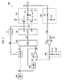
- FIG. 1 is a block diagram illustrating an overall configuration of a switching power supply device.
- FIG. 2 is a timing chart illustrating a basic operation of controlling pulse width modulation.
- FIG. 3 is a circuit diagram illustrating a configuration example of an overcurrent protection circuit.
- FIG. 4 is a timing chart illustrating an example of an overcurrent protection operation.
- FIG. 5 is a timing chart illustrating a problem of an overcurrent protection operation.
- FIG. 6 is a circuit diagram illustrating a first embodiment of a pulse skip circuit.
- FIG. 7 is a circuit diagram illustrating a configuration example of a frequency dividing part.
- FIG. 8 is a timing chart illustrating an example of a pulse skip operation.
- FIG. 9 is a view illustrating a comparison between behaviors of inductor currents in response to the presence and absence of a pulse skip operation.
- FIG. 10 is a circuit diagram illustrating a second embodiment of a pulse skip circuit.
- FIG. 11 is a circuit diagram illustrating a configuration example of a timer part.
- FIG. 12 is a timing chart illustrating a pulse skip operation in a high output time.
- FIG. 13 is a timing chart illustrating a pulse skip operation in a low output time.
- FIG. 14 is a waveform diagram illustrating a change behavior of a mask period in response to an output voltage.
- FIG. 15 is a circuit diagram illustrating a modification of a timer part.
- FIG. 16 is a timing chart illustrating an unintended pulse skip operation at the time of a high output.
- FIG. 17 is a circuit diagram illustrating a third embodiment of a pulse skip circuit.
- FIG. 18 is a timing chart illustrating a pulse skip operation in a high output time.
- FIG. 19 is a timing chart illustrating a pulse skip operation in a low output time.
- FIG. 20 is a view illustrating an appearance of a tablet terminal.
- FIG. 1 is block diagram illustrating an overall configuration of a switching power supply device.
- the switching power supply device 100 of this configuration example is a pulse width modulation (PWM) driven DC/DC converter for generating an output voltage Vo from an input voltage Vi and supplying the same to a load (a central processing unit (CPU) or the like) (not shown).
- the switching power supply device 100 includes a switching output circuit 110 , a feedback voltage generating circuit 120 , an error amplifier 130 , a phase compensation filter 140 , a clock signal generating circuit 150 , a slope voltage generating circuit 160 , a PWM comparator 170 , a control circuit 180 , a switch driving circuit 190 , an overcurrent protection circuit X, and a pulse skip circuit Y.
- any protection circuit an anti-low input malfunction circuit, a temperature protection circuit, and the like
- any protection circuit (an anti-low input malfunction circuit, a temperature protection circuit, and the like) other than the aforementioned circuit elements may also be incorporated in the switching power supply device
- the switching output circuit 110 is a step-down switching output stage that steps down an input voltage Vi to generate a desired output voltage Vo, and includes an output transistor 111 , a synchronous rectification transistor 112 , an output inductor 113 , and an output capacitor 114 .
- the output transistor 111 is a P channel type metal oxide semiconductor field effect transistor (PMOSFET) serving as an upper switch of the switching output stage.
- a source of the output transistor 111 is connected to an application terminal of the input voltage Vi.
- a drain of the output transistor 111 is connected to a first terminal of the output inductor 113 .
- a gate of the output transistor 111 is connected to an application terminal of an upper gate signal G 1 .
- the output transistor 111 is turned off when the upper gate signal G 1 has a high level and turned on when the upper gate signal G 1 has a low level.
- the synchronous rectification transistor 112 is an N channel type MOSFET (NMOSFET) serving as a lower switch of the switching output stage.
- a source of the synchronous rectification transistor 112 is connected to a ground terminal (an application terminal of a ground voltage GND).
- a drain of the synchronous rectification transistor 112 is connected to the first terminal of the output inductor 113 .
- a gate of the synchronous rectification transistor 112 is connected to an application terminal of the lower gate signal G 2 .
- the synchronous rectification transistor 112 is turned on when the lower gate signal G 2 has a high level and turned off when the lower gate signal G 2 has a low level.
- the output transistor 111 and the synchronous rectification transistor 112 are complementarily turned on and off depending on the upper gate signal G 1 and the lower gate signal G 2 .
- a switch voltage Vsw having a rectangular shape that is pulse-driven between the input voltage Vi and the ground voltage GND is generated in the first terminal of the output inductor 113 .
- the term “complementary” described above includes a case where a simultaneous OFF period (dead time) of the output transistor 111 and the synchronous rectification transistor 112 is provided, as well as a case where the ON/OFF states of both transistors are completely reversed.
- the output inductor 113 and the output capacitor 114 form an LC filter for rectifying or smoothing the switch voltage Vsw to generate the output voltage Vo.
- the first terminal of the output inductor 113 is connected to an application terminal of the switch voltage Vsw.
- Both a second terminal of the output inductor 113 and a first terminal of the output capacitor 114 are connected to an application terminal of the output voltage Vo.
- a second terminal of the output capacitor 114 is connected to the ground terminal.
- An output type of the switching output circuit 110 is not limited to the step-down type and may be any of a step-up type, a step-up/step-down type, and an inverting type. Also, a rectification scheme of the switching output circuit 110 is not limited to the synchronous rectification scheme and a diode rectification scheme using a rectification diode in place of the synchronous rectification transistor 112 may also be employed.
- a high breakdown voltage element such as a power MOSFET, an insulated gate bipolar transistor (IGBR), an SiC transistor, and the like may be used as the output transistor 111 and the synchronous rectification transistor 112 .
- the feedback voltage generating circuit 120 includes resistors 121 and 122 connected in series between the application terminal of the output voltage Vo and the ground terminal, and outputs a feedback voltage Vfb (a divided voltage of the output voltage Vo) depending on the output voltage Vo at a connection node between the both resistors. Further, when the output voltage Vo is within an input dynamic range of the error amplifier 130 , the feedback voltage generating circuit 120 may be omitted and the output voltage Vo may be directly input to the error amplifier 130 .
- the error amplifier 130 generates an error voltage V 1 corresponding to a difference between the feedback voltage Vfb applied to an inverting input terminal ( ⁇ ) and a reference voltage Vref applied to a non-inverting input terminal (+).
- the error voltage V 1 is increased when the feedback voltage Vfb is lower than the reference voltage Vref, and is decreased when the feedback voltage Vfb is higher than the reference voltage Vref.
- the phase compensation filter 140 includes a resistor 141 and a capacitor 142 connected in series between an application terminal of the error voltage V 1 and the ground terminal.
- the phase compensation filter 140 compensates for a phase of the error voltage V 1 to prevent oscillation of the error amplifier 130 .
- the slope voltage V 2 starts to rise in response to a falling edge of the clock signal S 0 , and is reset to a zero value in response to a rising edge of the OFF signal S 2 .
- an offset voltage obtained by simulating an inductor current IL (or an output current Io obtained by averaging the inductor current IL) flowing through the output inductor 113 may be added to the slope voltage V 2 .
- the PWM comparator 170 compares the error voltage V 1 applied to an inverting input terminal ( ⁇ ) and the slope voltage V 2 applied to a non-inverting input terminal (+) to generate the OFF signal S 2 .
- the OFF signal S 2 has a low level when the slope voltage V 2 is lower than the error voltage V 1 and has a high level when the slope voltage V 2 is higher than the error voltage V 1 .
- the control circuit 180 generates a pulse width modulation (PWM) signal S 3 based on an ON signal S 1 and the OFF signal S 2 .
- the PWM signal S 3 is set to a high level at a falling edge of the ON signal S 1 and reset to a low level at a rising edge of the OFF signal S 2 .
- the control circuit 180 also has a function of forcibly stopping a switching operation of the switching output circuit 110 in response to an overcurrent protection signal SX.
- the switch driving circuit 190 Upon receipt of the PWM signal S 3 , the switch driving circuit 190 generates an upper gate signal G 1 and a lower gate signal G 2 (equivalent to a driving signal of the switching output circuit 110 ).
- the upper gate signal G 1 and the lower gate signal G 2 basically have a low level when the PWM signal S 3 has a high level, and has a high level when the PWM signal S 3 has a low level.
- the overcurrent protection circuit X monitors the switch voltage Vsw and generates the overcurrent protection circuit SX indicating whether the inductor current IL flowing through the output inductor 113 is in an overcurrent state.
- the pulse skip circuit Y performs a pulse skip operation on the clock signal S 0 in response to the overcurrent protection signal SX, to generate the ON signal S 1 .
- FIG. 2 is a timing chart illustrating a basic operation of controlling pulse width modulation, in which the clock signal S 0 (i.e., ON signal S 1 ), the error voltage V 1 and the slope voltage V 2 , the OFF signal S 2 , and the PWM signal S 3 are illustrated in order from above.
- the clock signal S 0 i.e., ON signal S 1
- the error voltage V 1 and the slope voltage V 2 the OFF signal S 2
- the PWM signal S 3 PWM signal S 3
- the PWM signal S 3 is set to a high level.
- the output transistor 111 of the switching output circuit 110 is turned on and the synchronous rectification transistor 112 is turned off.
- the slope voltage V 2 starts to rise with a predetermined slope.
- a high level period Ton (an ON period of the output transistor 111 ) of the PWM signal S 3 is lengthened as the error voltage V 1 is higher, and shortened as the error voltage V 1 is lower.
- the PWM control is repeated, so that the output transistor 111 and the synchronous rectification transistor 112 of the switching output circuit 110 are periodically turned on and off to generate a desired output voltage Vo.
- FIG. 3 is a circuit diagram illustrating a configuration example of the overcurrent protection circuit X.
- the overcurrent protection circuit X of this configuration example includes an OCP comparator X 1 , a voltage source X 2 , a P channel type MOSFET X 3 , and a resistor X 4 .
- Both a positive terminal of the voltage source X 2 and a first terminal of the resistor X 4 are connected to an application terminal of an input voltage Vi.
- a negative terminal of the voltage source X 2 as an application terminal of a threshold voltage Vth ( ⁇ Vi) is connected to a non-inverting input terminal (+) of the OCP comparator X 1 .
- a second terminal of the resistor X 4 is connected to each of an inverting input terminal ( ⁇ ) of the OCP comparator X 1 and a source of the transistor X 3 .
- a drain of the transistor X 3 is connected to an application terminal of the switch voltage Vsw.
- a gate of the transistor X 3 is connected to an application terminal of the upper gate signal G 1 .
- the transistor X 3 is turned off during a high level period of the upper gate signal G 1 , and turned on during a low level period of the upper gate signal G 1 . In other words, the transistor X 3 is turned on and off in synchronization with the output transistor 111 .
- a monitor voltage Vm applied to the inverting input terminal ( ⁇ ) of the OCP comparator X 1 is equal to the high level of the switch voltage Vsw when the output transistor 111 is turned on, and is pulled up to the input voltage Vin through the resistor X 4 when the output transistor 111 is turned off.
- I an upper current flowing through the output transistor 111
- Ron an ON resistance of output transistor 111
- the OCP comparator X 1 it may be detected whether the upper current I flowing through the output transistor 111 (further, the inductor current IL flowing through the output inductor 113 ) is in an overcurrent state by comparing the monitor voltage Vim with the threshold voltage Vth by the OCP comparator X 1 .
- the overcurrent protection signal SX has a high level (i.e., a logic level when an overcurrent is detected) when the monitor voltage Vm is lower than the threshold voltage Vth, and has a low level (a logic level when an overcurrent is not detected) when the monitor voltage Vm is higher than the threshold voltage Vth.
- FIG. 4 is a timing chart illustrating an example of an overcurrent protection operation, in which the PWM signal S 3 and the inductor current IL (the solid line: overcurrent protection, the broken line: no overcurrent protection) are illustrated in order from above.
- the PWM signal S 3 and the inductor current IL the solid line: overcurrent protection, the broken line: no overcurrent protection
- a forcible-stop and self-return of the switching operation is repeated at every switching period T. That is to say, even though an overcurrent is detected during a certain period so that the switching operation of the switching output circuit 110 is forcibly stopped, the switching operation is self-returned (resumed) at a next period. Thus, even when the overcurrent protection is temporarily applied due to a variation in a load or the like, an output operation may be resumed.
- FIG. 5 is a timing chart illustrating a problem of an overcurrent protection operation, in which the PWM signal S 3 and the inductor current IL are illustrated in order from above.
- FIG. 5 for example, a behavior when the output terminal of the output voltage Vo is grounded through a path of low impedance in an application in which the input voltage Vi is high is illustrated.
- the pulse skip circuit Y is introduced as a solution to the problem.
- various embodiments of a configuration and an operation of the pulse skip circuit Y will be described in detail as an example.
- FIG. 6 is a circuit diagram illustrating a first embodiment of the pulse skip circuit Y.
- the pulse skip circuit Y of this embodiment includes a frequency dividing part Y 10 , an RS flipflop Y 20 , and an AND gate Y 30 .
- the frequency dividing part Y 10 starts a frequency dividing operation of the clock signal S 0 in response to the overcurrent protection signal SX to generate a mask period expiration signal SY 10 for determining an expiration timing of a mask period Tm.
- the RS flipflop Y 20 outputs a mask signal SY 20 from an inverting output terminal based on the overcurrent protection signal SX input to a set terminal and the mask period expiration signal SY 10 input to a reset terminal. For example, the RS flipflop Y 20 sets the mask signal SY 20 to a low level in response to a rising edge of the overcurrent protection signal SX and resets the mask signal SY 20 to a high level in response to a rising edge of the mask period expiration signal SY 10 .
- the AND gate Y 30 performs a logical AND operation on the clock signal S 0 and the mask signal SY 20 to generate the ON signal S 1 .
- the clock signal S 0 is through-output as the ON signal S 1 .
- the ON signal S 1 is fixed to a low level, without relying on a logic level of the clock signal S 0 .
- the AND gate Y 30 blocks the clock signal S 0 during a low level period (i.e., mask period Tm) of the mask signal SY 20 .
- FIG. 7 is a circuit diagram illustrating a configuration example of the frequency dividing part Y 10 .
- the frequency dividing part Y 10 of the present configuration example includes D flipflops Y 11 to Y 13 .
- a clock terminal of the D flipflop Y 11 is connected to an application terminal of the clock signal S 0 .
- An inverting output terminal of the D flipflop Y 11 is connected to a data terminal of the D flipflop Y 11 .
- a reset terminal of the D flipflop Y 11 is connected to an application terminal of the overcurrent protection signal SX.
- a frequency division clock signal SY 11 output from the inverting output terminal of the D flipflop Y 11 is for example a two-level signal (e.g., 1 ⁇ 2 frequency division signal of the clock signal S 0 ) which is reset to a high level in response to a rising edge of the overcurrent protection signal SX and subsequently alternately changed in a logic level at every rising edge of the clock signal S 0 .
- a clock terminal of the D flipflop Y 12 is connected to an application terminal of the frequency division clock signal SY 11 .
- An inverting output terminal of the D flipflop Y 12 is connected to a data terminal of the D flipflop Y 12 .
- a reset terminal of the D flipflop Y 12 is connected to an application terminal of the overcurrent protection signal SX.
- a frequency division clock signal SY 12 output from the inverting output terminal of the D flipflop Y 12 is for example a two-level signal (e.g., 1 ⁇ 4 frequency division signal of the clock signal S 0 ) which is reset to a high level in response to a rising edge of the overcurrent protection signal SX and subsequently alternately changed in a logic level at every rising edge of the frequency division clock signal SY 11 .
- a clock terminal of the D flipflop Y 13 is connected to an application terminal of the frequency division clock signal SY 12 .
- An inverting output terminal of the D flipflop Y 13 is connected to a data terminal of the D flipflop Y 13 .
- a reset terminal of the D flipflop Y 13 is connected to an application terminal of the overcurrent protection signal SX.
- a frequency division clock signal SY 13 output from the inverting output terminal of the D flipflop Y 13 is for example a two-level signal (e.g., 1 ⁇ 8 frequency division signal of the clock signal S 0 ) which is reset to a high level in response to a rising edge of the overcurrent protection signal SX and subsequently alternately changed in its logic level at every rising edge of the frequency division clock signal SY 12 .
- an output terminal of the D flipflop Y 13 corresponds to an output terminal of the mask period expiration signal SY 10 .
- the mask period expiration signal SY 10 is a two-level signal which falls to a low level in response to a rising edge of the overcurrent protection signal SX and rises to a high level in response to a rising edge of the frequency division clock signal SY 12 .
- FIG. 8 is a timing chart illustrating an example of the pulse skip operation, in which the clock signal S 0 , the overcurrent protection signal SX, the frequency division clock signals SY 11 to SY 13 , the mask period expiration signal SY 10 , the mask signal SY 20 , and the ON signal S 1 are illustrated in order from above. Further, times t 21 to t 25 indicate pulse generation timings of the clock signal S 0 , and an interval therebetween is a switching period T.
- the output transistor 111 is turned on at the time t 21 and the overcurrent protection signal SX subsequently rises to a high level at the time ta (i.e., a case where an overcurrent is detected) is now considered.
- the mask signal SY 20 is set to a low level in response to a rising edge of the overcurrent protection signal SX.
- the ON signal S 1 is fixed to a low level during a low level period (i.e., mask period Tm) of the mask signal SY 20 .
- all the D flipflops Y 11 to Y 13 are reset in response to the rising edge of the overcurrent protection signal SX.
- all the frequency division clock signals SY 11 to SY 13 rise to a high level and the mask period expiration signal SY 10 falls to a low level.
- the frequency division clock signal SY 11 is alternately changed in its logic level at every rising edge of the clock signal S 0 .
- the frequency division clock signal SY 11 falls to a low level at the time t 22 , rises to a high level at the time t 23 , falls to a low level at the time t 24 , and rises to a high level at the time t 25 .
- the frequency division clock signal SY 12 is alternately changed in its logic level at every rising edge of the frequency division clock signal SY 11 . In other words, the frequency division clock signal SY 12 falls to a low level at the time t 23 and rises to a high level at the time t 25 .
- Each of the frequency division clock signal SY 13 and the mask period expiration signal SY 10 is alternately changed in its logic level at every rising edge of the frequency division clock signal SY 12 .
- the frequency division clock signal SY 13 falls to a low level and the mask period expiration signal SY 10 rises to a high level.
- the mask signal SY 20 is reset to a high level in response to the rising edge of the mask period expiration signal SY 10 .
- the process is returned to a state where the clock signal S 0 is through-output as the ON signal S 1 .
- the mask period Tm may be within a range of 3 ⁇ T ⁇ Tm ⁇ 4 ⁇ T. Therefore, the operation of skipping pulses of the clock signal S 0 may be appropriately performed.
- the pulse skip number is not limited to “3” and, for example, the number of stages of the flipflops of the frequency dividing part Y 10 may be reduced and the pulse skip number may be “1” or “2”. Conversely, the number of stages of the flipflops of the dividing part Y 10 may be increased and the pulse skip number may be “4 or greater”.
- FIG. 9 is a view illustrating a comparison between behaviors of inductor currents IL in response to the presence and absence of a pulse skip operation.
- the solid line 0 SKIP indicates an inductor current when the pulse skip number is “0”
- the solid line 1 SKIP indicates an inductor current when the pulse skip number is “1”
- the solid line 3 SKIP indicates an inductor current when the pulse skip number is “3”.
- the inductor current IL hops and an overcurrent protection operation is applied.
- the pulse skip operation is not performed (the solid line 0 SKIP)
- limiting the overcurrent is delayed to cause the inductor current IL to be continuously increased as illustrated in FIG. 5 .
- the ON frequency of the output transistor 111 may be reduced and a forcible stop period of a switching operation may be lengthened, enhancing the pulse-by-pulse type overcurrent protection function.
- the pulse skip number may be set to a minimum number (e.g., “3”) as long as the peak value of the inductor current IL may be limited to the threshold current Ith or less.
- the pulse skip operation is always performed when an overcurrent is detected.
- a rapid decrease in the inductor current IL may easily occur to cause a defective operation of a load (see the solid line 3 SKIP near the time tgs).
- FIG. 10 is a circuit diagram illustrating a second embodiment of the pulse skip circuit Y.
- the pulse skip circuit Y of this embodiment is based on the first embodiment ( FIG. 6 ), but includes a timer part Y 40 instead of the frequency dividing part Y 10 .
- the same components as those of the first embodiment will be given the same reference numerals as those of FIG. 6 , and a redundant description thereof will be omitted and characteristic parts of the second embodiment will be mainly described hereinafter.
- the timer part Y 40 starts a counting operation in response to a falling edge of a mask signal SY 20 (further, a rising edge of the overcurrent protection signal SX) to generate a mask period expiration signal SY 40 for determining an expiration timing of the mask period Tm.
- the mask period expiration signal SY 40 is input to the reset terminal of the RS flipflop Y 20 . Further, the timer part Y 40 has a function of extending the mask period Tm as the output voltage Vo (or the feedback voltage Vfb) is lowered.
- FIG. 11 is a circuit diagram illustrating a configuration example of the timer part Y 40 .
- the timer part Y 40 of the present configuration example includes a current source Y 41 , a capacitor Y 42 , a charge/discharge switch Y 43 , a voltage source Y 44 , and a comparator Y 45 .
- the current source Y 41 generates a variable charge current Ic according to the output voltage Vo (or the feedback voltage Vfb). More specifically, the current source Y 41 reduces the charge current Ic as the output voltage Vo is lowered, and increases the charge current Ic as the output voltage Vo is increased.
- a first terminal of the capacitor Y 42 is connected to an output terminal of the current source Y 41 .
- a second terminal of the capacitor Y 42 is connected to a ground terminal.
- the charge/discharge switch Y 43 is a switch element for switching charging and discharging of the capacitor Y 42 by conducting/blocking both ends of the capacitor Y 42 in response to the mask signal SY 20 .
- the charge/discharge switch Y 43 is turned on during a high level period (i.e., non-mask period) of the mask signal SY 20 and turned off during a low level period (i.e., mask period) of the mask signal SY 20 .
- the voltage source Y 44 generates a predetermined threshold voltage VB.
- the comparator Y 45 compares the charge voltage VA input to a non-inverting input terminal (+) and the threshold voltage VB input to an inverting input terminal ( ⁇ ) to generate the mask period expiration signal SV 40 .
- the mask period expiration signal SV 40 has a high level when the charge voltage VA is higher than the threshold voltage VB and has a low level when the charge voltage VA is lower than the threshold voltage VB.
- a pulse skip operation of the second embodiment will be described by two separate cases where the output voltage Vo is relatively high (hereinafter, referred to as “a high output time”) and where the output voltage Vo is relatively low (hereinafter, referred to as “a low output time”).
- FIG. 12 is a timing chart illustrating a pulse skip operation (the pulse skip number is “0”) in a high output time, in which the clock signal S 0 , the overcurrent protection signal SX, the charge voltage VA and the threshold voltage VB, the mask period expiration signal SV 40 , the mask signal SY 20 , and the ON signal S 1 are illustrated in order from above. Further, times t 31 to t 35 indicate pulse generation timings of the clock signal S 0 , and an interval therebetween is a switching period T.
- the output transistor 111 is turned on at the time t 31 and the overcurrent protection signal SX subsequently rises to a high level (i.e., a case where an overcurrent is detected) at the time tb 1 is now considered.
- the mask signal SY 20 is set to a low level in response to the rising edge of the overcurrent protection signal SX.
- the charge/discharge switch Y 43 is turned off and the charge voltage VA starts to be increased. Also, the charge voltage VA is rapidly increased because the output voltage Vo is high. For example, when the output voltage Vo is kept near a target value thereof at the time of detecting an overcurrent, the charge voltage VA exceeds the threshold voltage VB and the mask period expiration signal SY 40 rises to a high level at time tb 2 earlier than the time t 32 (i.e., a pulse generation timing of the clock signal S 0 at a next period), as illustrated in FIG. 12 .
- the mask signal SY 20 is reset to a high level in response to the rising edge of the mask period expiration signal SY 40 . Further, even after the time t 32 , the aforementioned operation is repeated basically unless the output voltage Vo is changed.
- FIG. 13 is a timing chart illustrating a pulse skip operation (pulse skip number is “3”) in a low output time. Similar to FIG. 12 , the clock signal S 0 , the overcurrent protection signal SX, the charge voltage VA and the threshold voltage VB, the mask period expiration signal SY 40 , the mask signal SY 20 , and the ON signal S 1 are illustrated in order from above. Further, times t 41 to t 45 indicate pulse generation timings of the clock signal S 0 , and an interval therebetween is a switching period T.
- the output transistor 111 is turned on at the time t 41 and the overcurrent protection signal SX subsequently rises to a high level (i.e., a case where an overcurrent is detected) at the time tc 1 is now considered.
- the mask signal SY 20 is set to a low level in response to the rising edge of the overcurrent protection signal SX.
- the ON signal S 1 is fixed to a low level during a low level period (i.e., mask period Tm) of the mask signal SY 20 .
- the charge/discharge switch Y 43 is turned off and the charge voltage VA starts to be increased. Also, the charge voltage VA is gently increased because the output voltage Vo is low. For example, when the output voltage Vo is lowered from its target value at the time of detecting an overcurrent, the charge voltage VA does not exceed the threshold voltage VB even when the time t 42 arrives (i.e., a pulse generation timing of the clock signal S 0 at a next period), as illustrated in FIG. 13 . Thus, the mask period expiration signal SY 40 does not rise to a high level but is kept in the low level.
- the charge voltage VA continues to be gently increased and finally exceeds the threshold voltage VB at the time tc 2 (later than a time t 44 and earlier than the time t 45 ).
- the mask period expiration signal SY 40 rises to a high level, the mask signal SY 20 is reset to a high level.
- the process is returned to a state where the clock signal S 0 is through-output as the ON signal S 1 .
- FIG. 14 is a waveform diagram illustrating a change behavior of the mask period Tm in response to the output voltage Vo.
- the inductor current IL hops to apply an overcurrent protection operation.
- the output voltage Vo is lowered with the lapse of time, and accordingly, the mask period Tm is gradually lengthened.
- the pulse skip number is “0”, which is a state where a pulse skip operation has not been performed (see FIG. 12 above).
- the inductor current IL (further, the output current Io supplied to a load) is not rapidly lowered, making it difficult to cause a defective operation of the load (see a comparison between the solid line and the broken line of the inductor current IL in FIG. 14 ).
- the output voltage Vo is lowered with the lapse of time and the pulse skip number is increased to “1”, “2”, and “3” as the mask period Tm is lengthened.
- a pulse skip operation is performed (see FIG. 13 ).
- an ON frequency of the output transistor 111 may be reduced and a forcible stop period of a switching operation may be lengthened, it is possible to enhance the pulse-by-pulse type overcurrent protection function.
- FIG. 15 is a circuit diagram illustrating a modification of the timer part Y 40 .
- the timer part Y 40 of this modification basically has the same configuration as that of FIG. 11 , and features that the charge current Ic generated in a current source Y 41 is a fixed value and the threshold voltage VB generated in a voltage source Y 44 is a variable value. More specifically, the voltage source Y 44 increases the threshold voltage VB as the output voltage Vo is lowered, and decreases the threshold voltage VB as the output voltage Vo is increased.
- a timing at which the charge voltage VA and the threshold voltage VB cross each other i.e., a timing at which the mask period expiration signal SV 40 rises
- the mask period Tm may be shortened as the output voltage Vo is increased and lengthened as the output voltage Vo is lowered.
- timer part Y 40 by using an analog timer as the timer part Y 40 , it becomes possible to arbitrarily set the mask period Tm without using a clock for a high speed timer faster than the clock signal S 0 .
- a digital timer may also be used as the timer part Y 40 .
- FIG. 16 is a timing chart illustrating a problem (i.e., an unintended pulse skip operation in the high output time) when the second embodiment is employed. Similar to FIGS. 12 and 13 , the clock signal S 0 , the overcurrent protection signal SX, the charge voltage VA and the threshold voltage VB, the mask period expiration signal SV 40 , the mask signal SY 20 , and the ON signal S 1 are illustrated in order from above. Further, times t 51 to t 53 indicate pulse generation timings of the clock signal S 0 , and an interval therebetween is a switching period T.
- a problem i.e., an unintended pulse skip operation in the high output time
- the output transistor 111 is turned on at the time t 51 and the overcurrent protection signal SX is subsequently increased to a high level (i.e., a case where an overcurrent is detected) at the time td 1 is now considered.
- the mask signal SY 20 is set to a low level in response to the rising edge of the overcurrent protection signal SX.
- the charge/discharge switch Y 43 is turned off and the charge voltage VA starts to be increased. Further, when the output voltage Vo is kept near its target value at the time of detecting an overcurrent, the mask period Tm expires almost instantly. Thus, a pulse skip operation is originally not performed (see FIG. 12 above).
- the mask signal SY 20 is kept at a low level, and thereafter, at the time td 2 in which the mask period expiration signal SY 40 rises to a high level, the mask signal SY 20 is reset to a high level.
- the pulse of the clock signal S 0 generated at the time t 52 is unintentionally masked.
- an output ripple component may be increased and the inductor current IL (further, the output current Io) may be rapidly lowered.
- FIG. 17 is a circuit diagram illustrating a third embodiment of the pulse skip circuit.
- the pulse skip circuit Y of this embodiment is based on the second embodiment ( FIG. 10 ) and features that a D flipflop Y 50 is added and connection of each part is changed.
- the same components as those of the second embodiment will be given the same reference numerals as those of FIG. 10 , and a redundant description thereof will be omitted and characteristic parts of the third embodiment will be mainly described hereinafter.
- a clock terminal of the D flipflop Y 50 is connected to an application terminal of the overcurrent protection signal SX.
- a data terminal of the D flipflop Y 50 is connected to an application terminal of the mask signal SY 20 , i.e., the inverting output terminal of the RS flipflop Y 20 .
- An output terminal of the D flipflop Y 50 is an output terminal of a second mask signal SY 50 and connected to an input terminal of an AND gate Y 30 .
- a reset terminal of the D flipflop Y 50 is connected to an application terminal of the mask period expiration signal SV 40 , i.e., output terminal of the timer part Y 40 .
- the D flipflop Y 50 In response to the overcurrent protection signal SX, the D flipflop Y 50 connected in this manner latches the mask signal SY 20 to generate the second mask signal SY 50 . For example, when the overcurrent protection signal SX rises to a high level, if the mask signal SY 20 has a high level, the second mask signal SY 50 also has a high level. Meanwhile, when the overcurrent protection signal SX rises to a high level, if the mask signal SY 20 has a low level, the second mask signal SY 50 also has a low level. Further, the second mask signal SY 50 is reset to a low level in response to, for example, a rising edge of the mask period expiration signal SV 40 .
- a set terminal of the RS flipflop Y 20 is connected to an application terminal of the clock signal S 0 , rather than to the application terminal of the overcurrent protection signal SX.
- the mask signal SY 20 generated in the RS flipflop Y 20 is set to a low level in response to a rising edge of the clock signal S 0 and is reset to a high level in response to a rising edge of the mask period expiration signal SV 40 .
- the second mask signal SY 50 is input to an AND gate Y 30 .
- the AND gate Y 30 performs a logical AND operation on the clock signal S 0 and the second mask signal SY 50 to generate an ON signal S 1 .
- the clock signal S 0 is through-output as the ON signal S 1 .
- the ON signal S 1 is fixed to a low level, without relying on a logic level of the clock signal S 0 .
- the AND gate Y 30 blocks the clock signal S 0 during a low level period (i.e., mask period Tm) of the second mask signal SY 50 .
- the timer part Y 40 a circuit configuration or a connection relation thereof is not particularly changed.
- the mask signal SY 20 input from the RS flipflop Y 20 is set to a low level in response to a rising edge of the clock signal S 0 , rather than in response to a rising edge of the overcurrent protection signal SX.
- the timer part Y 40 starts a counting operation in response to the rising edge of the clock signal S 0 , rather than in response to the rising edge of the overcurrent protection signal SX.
- FIG. 18 is a timing chart illustrating a pulse skip operation (the pulse skip number is “0”) at a high output time, in which the clock signal S 0 , the charge voltage VA and the threshold voltage VB, the mask period expiration signal SY 40 , the mask signal SY 20 , the overcurrent protection signal SX, the second mask signal SY 50 , and the ON signal S 1 are illustrated in order from above. Further, times t 61 to t 65 indicate pulse generation timings of the clock signal S 0 , and an interval therebetween is a switching period T.
- the mask signal SY 20 is first set to a low level in response to the rising edge of the clock signal S 0 at the time t 61 .
- the charge/discharge switch Y 43 is turned off and the charge voltage VA starts to be increased. Also, the charge voltage VA is more rapidly increased because the output voltage Vo is high. For example, when the output voltage Vo is kept near its target value at the time of detecting an overcurrent, the charge voltage VA exceeds the threshold voltage VB and the mask period expiration signal SY 40 rises to a high level at the time te 1 immediately after the time t 61 (before the time te 2 ), as illustrated in FIG. 18 . As a result, in the RS flipflop Y 20 , the mask signal SY 20 is reset to a high level in response to the rising edge of the mask period expiration signal SY 40 .
- FIG. 19 is a timing chart illustrating a pulse skip operation (pulse skip number is “3”) in a low output time. Similar to FIG. 18 , the clock signal S 0 , the charge voltage VA and the threshold voltage VB, the mask period expiration signal SV 40 , the mask signal SY 20 , the overcurrent protection signal SX, the second mask signal SY 50 , and the ON signal S 1 are illustrated in order from above. Further, times t 71 to t 75 indicate pulse generation timings of the clock signal S 0 , and an interval therebetween is a switching period T.
- the output transistor 111 is turned on at the time t 71 and the overcurrent protection signal SX subsequently rises to a high level (i.e., a case where an overcurrent is detected) at the time tf 1 is now considered.
- the mask signal SY 20 is set to a low level in response to the rising edge of the mask signal SY 20 .
- the charge/discharge switch Y 43 is turned off and the charge voltage VA starts to be increased. Also, the charge voltage VA is more gently increased because the output voltage Vo is low. For example, when the output voltage Vo is lowered from its target value at the time of detecting an overcurrent, the charge voltage VA does not exceed the threshold voltage VB even when the time tf 1 at which the overcurrent protection signal SX rises to a high level arrives, as illustrated in FIG. 19 . Thus, the mask period expiration signal SV 40 does not rise to a high level and the mask signal SY 20 is kept in a low level.
- the ON signal S 1 is fixed to a low level during a low level period (i.e., mask period Tm) of the second mask signal SY 50 .
- the charge voltage VA continues to be gently increased and finally exceeds the threshold voltage VB at the time tf 2 (later than time t 74 and earlier than the time t 75 ).
- the mask period expiration signal SY 40 rises to a high level, both the mask signal SY 20 and the second mask signal SY 50 are reset to a high level.
- the process is returned to a state where the clock signal S 0 is through-output as the ON signal S 1 .
- the pulse skip number may be set to a value smaller than “3”.
- the pulse skip number may be set to a value greater than “3”, which is not different from the aforementioned second embodiment.
- FIG. 20 is a view illustrating an appearance of a tablet terminal.
- a tablet terminal A is an example of an electronic device on which the switching power supply device 100 described above is mounted.
- the target on which the switching power supply device 100 is mounted is not limited thereto, but it may also be appropriately mounted on any other electronic device.
- the present disclosure described herein can be utilized in all the switching power supply devices (for example, a power supply device for CPU having a high switching frequency).
Abstract
A switching power supply device includes: a switching output circuit configured to generate an output voltage from an input voltage; an oscillation circuit configured to generate a clock signal; a control circuit configured to control driving of the switching output circuit in synchronization with the clock signal; a pulse-by-pulse type overcurrent protection circuit configured to detect an overcurrent flowing through the switching output circuit to generate an overcurrent protection signal for forcibly stopping a switching operation of the switching output circuit; and a pulse skip circuit configured to perform a pulse skip operation of the clock signal in response to the overcurrent protection signal.
Description
This application is based upon and claims the benefit of priority from Japanese Patent Application No. 2015-254169, filed on Dec. 25, 2015, the entire contents of which are incorporated herein by reference.
The present disclosure relates to a switching power supply device.
Conventionally, most of switching power supply devices has an overcurrent protection circuit for forcibly stopping a switching operation of an output transistor when an overcurrent is detected. A typically used type of the overcurrent protection circuit is a pulse-by-pulse type in which a forcible-stop and self-return of a switching operation is repeated at every period.
However, sometimes an output fault (grounded output or the like) that an extremely large amount of overcurrent flows occurs, in the pulse-by-pulse type overcurrent protection circuit in which a forcible-stop and self-return (resume) of the switching operation is repeated. In this case, even though an ON time is shortened to a minimum at every switching period, limiting an overcurrent is still delayed. Thus, an inductor current is continually increased, leading to breakdown of a switching output circuit.
The present disclosure provides some embodiments of a switching power supply device capable of enhancing a pulse-by-pulse type overcurrent protection function.
According to one embodiment of the present disclosure, there is provided a switching power supply device, including: a switching output circuit configured to generate an output voltage from an input voltage; an oscillation circuit configured to generate a clock signal; a control circuit configured to control driving of the switching output circuit in synchronization with the clock signal; a pulse-by-pulse type overcurrent protection circuit configured to detect an overcurrent flowing through the switching output circuit to generate an overcurrent protection signal for forcibly stopping a switching operation of the switching output circuit; and a pulse skip circuit configured to perform a pulse skip operation of the clock signal in response to the overcurrent protection signal (first configuration).
In the device having the first configuration, the pulse skip circuit may include: a frequency dividing part configured to start a frequency dividing operation of the clock signal in response to the overcurrent protection signal to generate a mask period expiration signal; an RS flipflop configured to generate a mask signal set to a first logic level in response to the overcurrent protection signal and reset to a second logic level in response to the mask period expiration signal; and a logic gate configured to block the clock signal over a mask period during which the mask signal is set to the first logic level (second configuration).
In the device having the first configuration, the pulse skip circuit may include: a timer part configured to start a counting operation in response to the overcurrent protection signal to generate a mask period expiration signal; an RS flipflop configured to generate a mask signal set to a first logic level in response to the overcurrent protection signal and reset to a second logic level in response to the mask period expiration signal; and a logic gate configured to block the clock signal over a mask period during which the mask signal is set to the first logic level (third configuration).
In the device having the first configuration, the pulse skip circuit may include: a timer part configured to start a counting operation in response to the clock signal to generate a mask period expiration signal; an RS flipflop configured to generate a first mask signal set to a first logic level in response to the overcurrent protection signal and reset to a second logic level in response to the mask period expiration signal; a D flipflop configured to latch the first mask signal in response to the overcurrent protection signal to generate a second mask signal; and a logic gate configured to block the clock signal over a mask period during which the second mask signal is set to the first logic level (fourth configuration).
In the device having the fourth configuration, the second mask signal may be reset to the second logic level in response to the mask period expiration signal (fifth configuration).
In the device having the third or fourth configuration, the timer part may be configured to extend the mask period as the output voltage is lowered (sixth configuration).
In the device having the third or fourth configuration, the timer part may include: a current source configured to generate a charge current; a capacitor charged by the charge current; a charge/discharge switch configured to conduct and block between both ends of the capacitor in response to the mask signal; a voltage source configured to generate a threshold voltage; and a comparator configured to compare a charge voltage of the capacitor with the threshold voltage to generate an expiration timing signal (seventh configuration).
In the device having the seventh configuration, the current source may be configured to decrease the charge current as the output voltage is lowered (eighth configuration).
In the device having the seventh or eighth configuration, the voltage source may be configured to increase the threshold voltage as the output voltage is lowered (ninth configuration).
According to another embodiment of the present disclosure, there is provided an electronic device including the switching power supply device having any one of the first to ninth configurations (tenth configuration).
<Switching Power Supply Device>
The switching output circuit 110 is a step-down switching output stage that steps down an input voltage Vi to generate a desired output voltage Vo, and includes an output transistor 111, a synchronous rectification transistor 112, an output inductor 113, and an output capacitor 114.
The output transistor 111 is a P channel type metal oxide semiconductor field effect transistor (PMOSFET) serving as an upper switch of the switching output stage. A source of the output transistor 111 is connected to an application terminal of the input voltage Vi. A drain of the output transistor 111 is connected to a first terminal of the output inductor 113. A gate of the output transistor 111 is connected to an application terminal of an upper gate signal G1. The output transistor 111 is turned off when the upper gate signal G1 has a high level and turned on when the upper gate signal G1 has a low level.
The synchronous rectification transistor 112 is an N channel type MOSFET (NMOSFET) serving as a lower switch of the switching output stage. A source of the synchronous rectification transistor 112 is connected to a ground terminal (an application terminal of a ground voltage GND). A drain of the synchronous rectification transistor 112 is connected to the first terminal of the output inductor 113. A gate of the synchronous rectification transistor 112 is connected to an application terminal of the lower gate signal G2. The synchronous rectification transistor 112 is turned on when the lower gate signal G2 has a high level and turned off when the lower gate signal G2 has a low level.
The output transistor 111 and the synchronous rectification transistor 112 are complementarily turned on and off depending on the upper gate signal G1 and the lower gate signal G2. Through such ON/OFF operations, a switch voltage Vsw having a rectangular shape that is pulse-driven between the input voltage Vi and the ground voltage GND is generated in the first terminal of the output inductor 113. Further, the term “complementary” described above includes a case where a simultaneous OFF period (dead time) of the output transistor 111 and the synchronous rectification transistor 112 is provided, as well as a case where the ON/OFF states of both transistors are completely reversed.
The output inductor 113 and the output capacitor 114 form an LC filter for rectifying or smoothing the switch voltage Vsw to generate the output voltage Vo. The first terminal of the output inductor 113 is connected to an application terminal of the switch voltage Vsw. Both a second terminal of the output inductor 113 and a first terminal of the output capacitor 114 are connected to an application terminal of the output voltage Vo. A second terminal of the output capacitor 114 is connected to the ground terminal.
An output type of the switching output circuit 110 is not limited to the step-down type and may be any of a step-up type, a step-up/step-down type, and an inverting type. Also, a rectification scheme of the switching output circuit 110 is not limited to the synchronous rectification scheme and a diode rectification scheme using a rectification diode in place of the synchronous rectification transistor 112 may also be employed.
Further, when a high voltage is applied to the switching output circuit 110, a high breakdown voltage element such as a power MOSFET, an insulated gate bipolar transistor (IGBR), an SiC transistor, and the like may be used as the output transistor 111 and the synchronous rectification transistor 112.
The feedback voltage generating circuit 120 includes resistors 121 and 122 connected in series between the application terminal of the output voltage Vo and the ground terminal, and outputs a feedback voltage Vfb (a divided voltage of the output voltage Vo) depending on the output voltage Vo at a connection node between the both resistors. Further, when the output voltage Vo is within an input dynamic range of the error amplifier 130, the feedback voltage generating circuit 120 may be omitted and the output voltage Vo may be directly input to the error amplifier 130.
The error amplifier 130 generates an error voltage V1 corresponding to a difference between the feedback voltage Vfb applied to an inverting input terminal (−) and a reference voltage Vref applied to a non-inverting input terminal (+). The error voltage V1 is increased when the feedback voltage Vfb is lower than the reference voltage Vref, and is decreased when the feedback voltage Vfb is higher than the reference voltage Vref.
The phase compensation filter 140 includes a resistor 141 and a capacitor 142 connected in series between an application terminal of the error voltage V1 and the ground terminal. The phase compensation filter 140 compensates for a phase of the error voltage V1 to prevent oscillation of the error amplifier 130.
The clock signal generating circuit 150 generates a clock signal S0 that is pulse-driven at a predetermined switching frequency fsw (=1/T).
Upon receipt of the clock signal S0 and an OFF signal S2, the slope voltage generating circuit 160 generates a slope voltage V2 having a triangular wave, a sawtooth wave, or an n order slope wave (e.g., n=2). The slope voltage V2 starts to rise in response to a falling edge of the clock signal S0, and is reset to a zero value in response to a rising edge of the OFF signal S2.
Further, an offset voltage obtained by simulating an inductor current IL (or an output current Io obtained by averaging the inductor current IL) flowing through the output inductor 113 may be added to the slope voltage V2. By employing such a configuration, it becomes possible to realize a current mode control, increasing load responsiveness.
The PWM comparator 170 compares the error voltage V1 applied to an inverting input terminal (−) and the slope voltage V2 applied to a non-inverting input terminal (+) to generate the OFF signal S2. The OFF signal S2 has a low level when the slope voltage V2 is lower than the error voltage V1 and has a high level when the slope voltage V2 is higher than the error voltage V1.
The control circuit 180 generates a pulse width modulation (PWM) signal S3 based on an ON signal S1 and the OFF signal S2. The PWM signal S3 is set to a high level at a falling edge of the ON signal S1 and reset to a low level at a rising edge of the OFF signal S2. Further, the control circuit 180 also has a function of forcibly stopping a switching operation of the switching output circuit 110 in response to an overcurrent protection signal SX.
Upon receipt of the PWM signal S3, the switch driving circuit 190 generates an upper gate signal G1 and a lower gate signal G2 (equivalent to a driving signal of the switching output circuit 110). The upper gate signal G1 and the lower gate signal G2 basically have a low level when the PWM signal S3 has a high level, and has a high level when the PWM signal S3 has a low level.
The overcurrent protection circuit X monitors the switch voltage Vsw and generates the overcurrent protection circuit SX indicating whether the inductor current IL flowing through the output inductor 113 is in an overcurrent state.
The pulse skip circuit Y performs a pulse skip operation on the clock signal S0 in response to the overcurrent protection signal SX, to generate the ON signal S1.
<PWM Control>
At time t11, when the clock signal S0 falls to a low level, the PWM signal S3 is set to a high level. As a result, the output transistor 111 of the switching output circuit 110 is turned on and the synchronous rectification transistor 112 is turned off. Further, at the time t11, when the clock signal S0 falls to a low level, the slope voltage V2 starts to rise with a predetermined slope.
At time t12, when the slope voltage V2 is higher than the error voltage V1 so that the OFF signal S2 rises to a high level, the PWM signal W3 is reset to a low level. As a result, the output transistor 111 of the switching output circuit 110 is turned off and the synchronous rectification transistor 112 is turned on. Further, at the time t12, when the OFF signal S2 rises to a high level, the slope voltage V2 is rapidly discharged.
Through the above-described PWM control, a high level period Ton (an ON period of the output transistor 111) of the PWM signal S3 is lengthened as the error voltage V1 is higher, and shortened as the error voltage V1 is lower. In other words, the duty D (=Ton×1/T) of the PWM signal S3 is increased as the error voltage V1 is higher, and shortened as the error voltage V1 is lower.
Further, even after time t13 at which the clock signal S0 falls again to a low level, the PWM control is repeated, so that the output transistor 111 and the synchronous rectification transistor 112 of the switching output circuit 110 are periodically turned on and off to generate a desired output voltage Vo.
<Overcurrent Protection Circuit>
Both a positive terminal of the voltage source X2 and a first terminal of the resistor X4 are connected to an application terminal of an input voltage Vi. A negative terminal of the voltage source X2 as an application terminal of a threshold voltage Vth (<Vi) is connected to a non-inverting input terminal (+) of the OCP comparator X1. A second terminal of the resistor X4 is connected to each of an inverting input terminal (−) of the OCP comparator X1 and a source of the transistor X3. A drain of the transistor X3 is connected to an application terminal of the switch voltage Vsw. A gate of the transistor X3 is connected to an application terminal of the upper gate signal G1.
In the overcurrent protection circuit X having this configuration, the transistor X3 is turned off during a high level period of the upper gate signal G1, and turned on during a low level period of the upper gate signal G1. In other words, the transistor X3 is turned on and off in synchronization with the output transistor 111. Thus, a monitor voltage Vm applied to the inverting input terminal (−) of the OCP comparator X1 is equal to the high level of the switch voltage Vsw when the output transistor 111 is turned on, and is pulled up to the input voltage Vin through the resistor X4 when the output transistor 111 is turned off.
Further, the monitor voltage Vm obtained when the output transistor 111 is turned on has a voltage value obtained by subtracting a voltage across the output transistor 111 from the input voltage Vi (=Vi−I×Ron) (where I is an upper current flowing through the output transistor 111 and Ron is an ON resistance of output transistor 111). In other words, when the ON resistance Ron of the output transistor 111 is regarded as a predetermined value, the monitor voltage Vm obtained when the output transistor 111 is turned on is lowered as the upper current I is increased.
Thus, it may be detected whether the upper current I flowing through the output transistor 111 (further, the inductor current IL flowing through the output inductor 113) is in an overcurrent state by comparing the monitor voltage Vim with the threshold voltage Vth by the OCP comparator X1.
More specifically, the overcurrent protection signal SX has a high level (i.e., a logic level when an overcurrent is detected) when the monitor voltage Vm is lower than the threshold voltage Vth, and has a low level (a logic level when an overcurrent is not detected) when the monitor voltage Vm is higher than the threshold voltage Vth. In other words, the overcurrent protection signal SX has a high level when the inductor current IL is greater than a threshold current Ith (=(Vi−Vth)/Ron), and has a low level when the inductor current IL is smaller than the threshold current Ith.
In the configuration of generating the overcurrent protection signal SX by monitoring the switch voltage Vsw in this manner, it is not necessary to insert a sense resistor in the current path through which the inductor current IL flows, reducing the cost and enhancing the output efficiency.
<Overcurrent Protection Operation (Basis)>
Hereinafter, an overcurrent protection operation when the pulse skip circuit Y is not introduced (i.e., when the clock signal S0 is directly input as the ON signal S1 to the control circuit 180) will be first described with reference to FIGS. 4 and 5 in order to clarify the purpose of introducing the pulse skip circuit Y.
In the overcurrent protection operation of FIG. 4 , when the inductor current IL is greater than the predetermined threshold current Ith, the PWM signal S3 forcibly falls to a low level. As a result, since a switching operation of the switching output circuit 110 is forcibly stopped, a peak value of the inductor current IL is limited not to exceed the threshold current Ith.
In particular, in the pulse-by-pulse type overcurrent protection operation, a forcible-stop and self-return of the switching operation is repeated at every switching period T. That is to say, even though an overcurrent is detected during a certain period so that the switching operation of the switching output circuit 110 is forcibly stopped, the switching operation is self-returned (resumed) at a next period. Thus, even when the overcurrent protection is temporarily applied due to a variation in a load or the like, an output operation may be resumed.
When the output is grounded, in the pulse-by-pulse type overcurrent protection operation in which forcible-stop and self-return (resume) of the switching operation is repeated, even though the ON time Ton is shortened to a minimum (i.e., minimum ON period Ton (min)) at every switching period T, limiting the overcurrent (i.e., reducing the inductor current IL during a forcible OFF period) may be delayed to cause the inductor current IL to be continuously increased, leading to breakdown of the switching output circuit 110.
As one approach to enhance the overcurrent protection function, shortening the minimum ON period Ton (min) by minimizing a signal delay of the OCP comparator X1 is considered. However, in order to reduce the signal delay of the OCP comparator X1, it is necessary to increase a driving current, which is disadvantageous in promoting the power saving of the switching power supply device 100. In addition, no matter how the driving current of the OCP comparator X1 is increased, it is impossible to completely make the signal delay zero. Thus, minimizing the signal delay is not a basic solution of the problem.
Thus, in the switching power supply device 100, the pulse skip circuit Y is introduced as a solution to the problem. Hereinafter, various embodiments of a configuration and an operation of the pulse skip circuit Y will be described in detail as an example.
The frequency dividing part Y10 starts a frequency dividing operation of the clock signal S0 in response to the overcurrent protection signal SX to generate a mask period expiration signal SY10 for determining an expiration timing of a mask period Tm.
The RS flipflop Y20 outputs a mask signal SY20 from an inverting output terminal based on the overcurrent protection signal SX input to a set terminal and the mask period expiration signal SY10 input to a reset terminal. For example, the RS flipflop Y20 sets the mask signal SY20 to a low level in response to a rising edge of the overcurrent protection signal SX and resets the mask signal SY20 to a high level in response to a rising edge of the mask period expiration signal SY10.
The AND gate Y30 performs a logical AND operation on the clock signal S0 and the mask signal SY20 to generate the ON signal S1. When the mask signal SY20 has a high level, the clock signal S0 is through-output as the ON signal S1. Meanwhile, when the mask signal SY20 has a low level, the ON signal S1 is fixed to a low level, without relying on a logic level of the clock signal S0. In other words, the AND gate Y30 blocks the clock signal S0 during a low level period (i.e., mask period Tm) of the mask signal SY20.
A clock terminal of the D flipflop Y11 is connected to an application terminal of the clock signal S0. An inverting output terminal of the D flipflop Y11 is connected to a data terminal of the D flipflop Y11. A reset terminal of the D flipflop Y11 is connected to an application terminal of the overcurrent protection signal SX. A frequency division clock signal SY11 output from the inverting output terminal of the D flipflop Y11 is for example a two-level signal (e.g., ½ frequency division signal of the clock signal S0) which is reset to a high level in response to a rising edge of the overcurrent protection signal SX and subsequently alternately changed in a logic level at every rising edge of the clock signal S0.
A clock terminal of the D flipflop Y12 is connected to an application terminal of the frequency division clock signal SY11. An inverting output terminal of the D flipflop Y12 is connected to a data terminal of the D flipflop Y12. A reset terminal of the D flipflop Y12 is connected to an application terminal of the overcurrent protection signal SX. A frequency division clock signal SY12 output from the inverting output terminal of the D flipflop Y12 is for example a two-level signal (e.g., ¼ frequency division signal of the clock signal S0) which is reset to a high level in response to a rising edge of the overcurrent protection signal SX and subsequently alternately changed in a logic level at every rising edge of the frequency division clock signal SY11.
A clock terminal of the D flipflop Y13 is connected to an application terminal of the frequency division clock signal SY12. An inverting output terminal of the D flipflop Y13 is connected to a data terminal of the D flipflop Y13. A reset terminal of the D flipflop Y13 is connected to an application terminal of the overcurrent protection signal SX. A frequency division clock signal SY13 output from the inverting output terminal of the D flipflop Y13 is for example a two-level signal (e.g., ⅛ frequency division signal of the clock signal S0) which is reset to a high level in response to a rising edge of the overcurrent protection signal SX and subsequently alternately changed in its logic level at every rising edge of the frequency division clock signal SY12.
Further, an output terminal of the D flipflop Y13 corresponds to an output terminal of the mask period expiration signal SY10. In other words, the mask period expiration signal SY10 is a two-level signal which falls to a low level in response to a rising edge of the overcurrent protection signal SX and rises to a high level in response to a rising edge of the frequency division clock signal SY12.
A case where the output transistor 111 is turned on at the time t21 and the overcurrent protection signal SX subsequently rises to a high level at the time ta (i.e., a case where an overcurrent is detected) is now considered. In this case, in the RS flipflop Y20, the mask signal SY20 is set to a low level in response to a rising edge of the overcurrent protection signal SX. Thus, after the time ta, the ON signal S1 is fixed to a low level during a low level period (i.e., mask period Tm) of the mask signal SY20.
Further, in the frequency dividing part Y10, all the D flipflops Y11 to Y13 are reset in response to the rising edge of the overcurrent protection signal SX. Thus, all the frequency division clock signals SY11 to SY13 rise to a high level and the mask period expiration signal SY10 falls to a low level.
Thereafter, the frequency division clock signal SY11 is alternately changed in its logic level at every rising edge of the clock signal S0. In other words, the frequency division clock signal SY11 falls to a low level at the time t22, rises to a high level at the time t23, falls to a low level at the time t24, and rises to a high level at the time t25.
The frequency division clock signal SY12 is alternately changed in its logic level at every rising edge of the frequency division clock signal SY11. In other words, the frequency division clock signal SY12 falls to a low level at the time t23 and rises to a high level at the time t25.
Each of the frequency division clock signal SY13 and the mask period expiration signal SY10 is alternately changed in its logic level at every rising edge of the frequency division clock signal SY12. In other words, at the time t25 at which the frequency division clock signal SY12 rises to a high level, the frequency division clock signal SY13 falls to a low level and the mask period expiration signal SY10 rises to a high level.
As a result, in the RS flipflop Y20, the mask signal SY20 is reset to a high level in response to the rising edge of the mask period expiration signal SY10. Thus, after the time t25, the process is returned to a state where the clock signal S0 is through-output as the ON signal S1.
Through the series of pulse skip operations, three pulses of the clock signal S0 are skipped during the mask period Tm from the time to to the time t25.
Further, as mentioned above, in the frequency dividing part Y10, an operation of frequency-dividing the clock signal S0 always starts from an initial state (SY11=SY12=SY13=H, SY10=L) in response to the rising edge of the overcurrent protection signal SX. Thus, no matter at which timing an overcurrent is detected, the mask period Tm may be within a range of 3×T<Tm<4×T. Therefore, the operation of skipping pulses of the clock signal S0 may be appropriately performed.
Further, the pulse skip number is not limited to “3” and, for example, the number of stages of the flipflops of the frequency dividing part Y10 may be reduced and the pulse skip number may be “1” or “2”. Conversely, the number of stages of the flipflops of the dividing part Y10 may be increased and the pulse skip number may be “4 or greater”.
When the output terminal of the output voltage Vo is grounded through a path of low impedance at time tgs, the inductor current IL hops and an overcurrent protection operation is applied. Here, when the pulse skip operation is not performed (the solid line 0SKIP), limiting the overcurrent is delayed to cause the inductor current IL to be continuously increased as illustrated in FIG. 5 .
Meanwhile, when the pulse skip operation is performed (the solid line 1SKIP or the solid line 3SKIP), the ON frequency of the output transistor 111 may be reduced and a forcible stop period of a switching operation may be lengthened, enhancing the pulse-by-pulse type overcurrent protection function.
As the pulse skip number increases, the overcurrent protection function may be enhanced, while a ripple component of the inductor current IL is increased. Thus, in some embodiments, the pulse skip number may be set to a minimum number (e.g., “3”) as long as the peak value of the inductor current IL may be limited to the threshold current Ith or less.
However, in the pulse skip circuit Y of this embodiment, the pulse skip operation is always performed when an overcurrent is detected. Thus, it should be noted that, at the time of transition from a normal operation to the overcurrent protection operation, a rapid decrease in the inductor current IL (further, the output current Io supplied to a load) may easily occur to cause a defective operation of a load (see the solid line 3 SKIP near the time tgs).
The timer part Y40 starts a counting operation in response to a falling edge of a mask signal SY20 (further, a rising edge of the overcurrent protection signal SX) to generate a mask period expiration signal SY40 for determining an expiration timing of the mask period Tm. The mask period expiration signal SY40 is input to the reset terminal of the RS flipflop Y20. Further, the timer part Y40 has a function of extending the mask period Tm as the output voltage Vo (or the feedback voltage Vfb) is lowered.
The current source Y41 generates a variable charge current Ic according to the output voltage Vo (or the feedback voltage Vfb). More specifically, the current source Y41 reduces the charge current Ic as the output voltage Vo is lowered, and increases the charge current Ic as the output voltage Vo is increased.
A first terminal of the capacitor Y42 is connected to an output terminal of the current source Y41. A second terminal of the capacitor Y42 is connected to a ground terminal. When the charge/discharge switch Y43 is in an OFF state, the capacitor Y42 is charged by the charge current Ic and a charge voltage VA appearing at the first terminal of the capacitor Y42 is increased. Meanwhile, when the charge/discharge switch Y43 is in an ON state, the capacitor Y42 is discharged through the charge/discharge switch Y43 and the charge voltage VA is lowered.
The charge/discharge switch Y43 is a switch element for switching charging and discharging of the capacitor Y42 by conducting/blocking both ends of the capacitor Y42 in response to the mask signal SY20. The charge/discharge switch Y43 is turned on during a high level period (i.e., non-mask period) of the mask signal SY20 and turned off during a low level period (i.e., mask period) of the mask signal SY20.
The voltage source Y44 generates a predetermined threshold voltage VB.
The comparator Y45 compares the charge voltage VA input to a non-inverting input terminal (+) and the threshold voltage VB input to an inverting input terminal (−) to generate the mask period expiration signal SV40. The mask period expiration signal SV40 has a high level when the charge voltage VA is higher than the threshold voltage VB and has a low level when the charge voltage VA is lower than the threshold voltage VB.
Next, a pulse skip operation of the second embodiment will be described by two separate cases where the output voltage Vo is relatively high (hereinafter, referred to as “a high output time”) and where the output voltage Vo is relatively low (hereinafter, referred to as “a low output time”).
A case where the output transistor 111 is turned on at the time t31 and the overcurrent protection signal SX subsequently rises to a high level (i.e., a case where an overcurrent is detected) at the time tb1 is now considered. In this case, in the RS flipflop Y20, the mask signal SY20 is set to a low level in response to the rising edge of the overcurrent protection signal SX.
At this time, in the timer part Y40, the charge/discharge switch Y43 is turned off and the charge voltage VA starts to be increased. Also, the charge voltage VA is rapidly increased because the output voltage Vo is high. For example, when the output voltage Vo is kept near a target value thereof at the time of detecting an overcurrent, the charge voltage VA exceeds the threshold voltage VB and the mask period expiration signal SY40 rises to a high level at time tb2 earlier than the time t32 (i.e., a pulse generation timing of the clock signal S0 at a next period), as illustrated in FIG. 12 .
As a result, in the RS flipflop Y20, the mask signal SY20 is reset to a high level in response to the rising edge of the mask period expiration signal SY40. Further, even after the time t32, the aforementioned operation is repeated basically unless the output voltage Vo is changed.
In this manner, in FIG. 12 , once the mask signal SY20 falls to a low level upon detection of an overcurrent but rises to a high level again before a next pulse of the clock signal S0 is generated. Thus, since a pulse of the clock signal S0 does not arrive during the low level period (i.e., mask period Tm) of the mask signal SY20, the pulse skip number is “0”. In other words, the same overcurrent protection operation as that of the existing case where forcible stop and self-return (resume) of the switching operation are repeated at every switching period T is performed.
A case where the output transistor 111 is turned on at the time t41 and the overcurrent protection signal SX subsequently rises to a high level (i.e., a case where an overcurrent is detected) at the time tc1 is now considered. In this case, in the RS flipflop Y20, the mask signal SY20 is set to a low level in response to the rising edge of the overcurrent protection signal SX. Thus, after the time tc1, the ON signal S1 is fixed to a low level during a low level period (i.e., mask period Tm) of the mask signal SY20.
At this time, in the timer part Y40, the charge/discharge switch Y43 is turned off and the charge voltage VA starts to be increased. Also, the charge voltage VA is gently increased because the output voltage Vo is low. For example, when the output voltage Vo is lowered from its target value at the time of detecting an overcurrent, the charge voltage VA does not exceed the threshold voltage VB even when the time t42 arrives (i.e., a pulse generation timing of the clock signal S0 at a next period), as illustrated in FIG. 13 . Thus, the mask period expiration signal SY40 does not rise to a high level but is kept in the low level.
Thereafter, the charge voltage VA continues to be gently increased and finally exceeds the threshold voltage VB at the time tc2 (later than a time t44 and earlier than the time t45). As a result, since the mask period expiration signal SY40 rises to a high level, the mask signal SY20 is reset to a high level. Thus, after the time tc2, the process is returned to a state where the clock signal S0 is through-output as the ON signal S1.
Through the series of pulse skip operations, three pulses of the clock signal S0 are skipped during the mask period Tm from the time tc1 to the time tc2. When the output voltage Vo is further increased, the charge current Ic may be further increased and the mask period Tm may be shortened, so that the pulse skip number may be set to a value smaller than “3”. Conversely, when the output voltage Vo is further lowered, the charge current Ic may be further decreased and the mask period Tm may be lengthened, so that the pulse skip number may be set to a value greater than “3”.
For example, since the output voltage Vo is not much lowered immediately after the time tgs, the pulse skip number is “0”, which is a state where a pulse skip operation has not been performed (see FIG. 12 above). Thus, even when a normal operation transitions to an overcurrent protection operation, the inductor current IL (further, the output current Io supplied to a load) is not rapidly lowered, making it difficult to cause a defective operation of the load (see a comparison between the solid line and the broken line of the inductor current IL in FIG. 14 ).
Thereafter, the output voltage Vo is lowered with the lapse of time and the pulse skip number is increased to “1”, “2”, and “3” as the mask period Tm is lengthened. In this state, a pulse skip operation is performed (see FIG. 13 ). Thus, since an ON frequency of the output transistor 111 may be reduced and a forcible stop period of a switching operation may be lengthened, it is possible to enhance the pulse-by-pulse type overcurrent protection function.
Further, as a method for enhancing the pulse-by-pulse type overcurrent protection function, a configuration in which the switching frequency fsw itself is lowered as the output voltage Vo is lowered is also considered. In this configuration, however, since an output ripple component is increased even in an operation start time with the low output voltage Vo as well as in the overcurrent protection operation, a countermeasure is required. Meanwhile, in this configuration, the mask period Tm for pulse skipping is simply changed depending on the output voltage Vo when an overcurrent protection operation is applied. Thus, a problem of the operation start time does not arise.
Also when this modification is employed, a timing at which the charge voltage VA and the threshold voltage VB cross each other (i.e., a timing at which the mask period expiration signal SV40 rises) becomes earlier as the output voltage Vo is increased and delayed as the output voltage Vo is lowered. Thus, like the example illustrated in FIG. 11 , the mask period Tm may be shortened as the output voltage Vo is increased and lengthened as the output voltage Vo is lowered.
Further, as illustrated in FIGS. 11 and 15 , by using an analog timer as the timer part Y40, it becomes possible to arbitrarily set the mask period Tm without using a clock for a high speed timer faster than the clock signal S0. However, when a clock for a high speed timer is separately provided, a digital timer may also be used as the timer part Y40.
A case where the output transistor 111 is turned on at the time t51 and the overcurrent protection signal SX is subsequently increased to a high level (i.e., a case where an overcurrent is detected) at the time td1 is now considered. In this case, in the RS flipflop Y20, the mask signal SY20 is set to a low level in response to the rising edge of the overcurrent protection signal SX.
At this time, in the timer part Y40, the charge/discharge switch Y43 is turned off and the charge voltage VA starts to be increased. Further, when the output voltage Vo is kept near its target value at the time of detecting an overcurrent, the mask period Tm expires almost instantly. Thus, a pulse skip operation is originally not performed (see FIG. 12 above).
However, when the time td1 is immediately before the time t52, namely, when a timing at which an overcurrent is detected is immediately before a timing at which a pulse of the clock signal S0 is generated at a next period, a situation in which the charge voltage VA does not exceed the threshold voltage VB or a situation in which the charge voltage VA exceeds the threshold voltage VB but the mask period expiration signal SY40 does not rise to a high level due to a signal delay of the comparator Y45 or the like may occur at the time t52.
In this situation, at the time t52 in which a pulse of the clock signal S0 is generated, the mask signal SY20 is kept at a low level, and thereafter, at the time td2 in which the mask period expiration signal SY40 rises to a high level, the mask signal SY20 is reset to a high level. In other words, the pulse of the clock signal S0 generated at the time t52 is unintentionally masked. Thus, an output ripple component may be increased and the inductor current IL (further, the output current Io) may be rapidly lowered.
In this manner, in the second embodiment, extremely rarely, a pulse skip operation which is not to be performed originally may be performed unintentionally. Hereinafter, a third embodiment capable of resolving the problem is proposed.
A clock terminal of the D flipflop Y50 is connected to an application terminal of the overcurrent protection signal SX. A data terminal of the D flipflop Y50 is connected to an application terminal of the mask signal SY20, i.e., the inverting output terminal of the RS flipflop Y20. An output terminal of the D flipflop Y50 is an output terminal of a second mask signal SY50 and connected to an input terminal of an AND gate Y30. A reset terminal of the D flipflop Y50 is connected to an application terminal of the mask period expiration signal SV40, i.e., output terminal of the timer part Y40.
In response to the overcurrent protection signal SX, the D flipflop Y50 connected in this manner latches the mask signal SY20 to generate the second mask signal SY50. For example, when the overcurrent protection signal SX rises to a high level, if the mask signal SY20 has a high level, the second mask signal SY50 also has a high level. Meanwhile, when the overcurrent protection signal SX rises to a high level, if the mask signal SY20 has a low level, the second mask signal SY50 also has a low level. Further, the second mask signal SY50 is reset to a low level in response to, for example, a rising edge of the mask period expiration signal SV40.
According to the addition of the D flipflop Y50, a set terminal of the RS flipflop Y20 is connected to an application terminal of the clock signal S0, rather than to the application terminal of the overcurrent protection signal SX. In other words, the mask signal SY20 generated in the RS flipflop Y20 is set to a low level in response to a rising edge of the clock signal S0 and is reset to a high level in response to a rising edge of the mask period expiration signal SV40.
Also, according to the addition of the D flipflop Y50, the second mask signal SY50, rather than the mask signal SY20, is input to an AND gate Y30. In other words, the AND gate Y30 performs a logical AND operation on the clock signal S0 and the second mask signal SY50 to generate an ON signal S1. When the second mask signal SY50 has a high level, the clock signal S0 is through-output as the ON signal S1. Meanwhile, when the second mask signal SY50 has a low level, the ON signal S1 is fixed to a low level, without relying on a logic level of the clock signal S0. In other words, the AND gate Y30 blocks the clock signal S0 during a low level period (i.e., mask period Tm) of the second mask signal SY50.
Regarding the timer part Y40, a circuit configuration or a connection relation thereof is not particularly changed. However, as mentioned above, according to the addition of the D flipflop Y50, the mask signal SY20 input from the RS flipflop Y20 is set to a low level in response to a rising edge of the clock signal S0, rather than in response to a rising edge of the overcurrent protection signal SX. Thus, the timer part Y40 starts a counting operation in response to the rising edge of the clock signal S0, rather than in response to the rising edge of the overcurrent protection signal SX.
Next, a pulse skip operation of the third embodiment will be described by two separate cases where the output voltage Vo is relatively high (hereinafter, referred to as “at a high output time”) and when the output voltage Io is relatively low (hereinafter, referred to as “at a low output time”).
A case where the output transistor 111 is turned on at the time t61 and the overcurrent protection signal SX subsequently rises to a high level (i.e., a case where an overcurrent is detected) at the time te2 is now considered. In this case, the mask signal SY20 is first set to a low level in response to the rising edge of the clock signal S0 at the time t61.
At this time, in the timer part Y40, the charge/discharge switch Y43 is turned off and the charge voltage VA starts to be increased. Also, the charge voltage VA is more rapidly increased because the output voltage Vo is high. For example, when the output voltage Vo is kept near its target value at the time of detecting an overcurrent, the charge voltage VA exceeds the threshold voltage VB and the mask period expiration signal SY40 rises to a high level at the time te1 immediately after the time t61 (before the time te2), as illustrated in FIG. 18 . As a result, in the RS flipflop Y20, the mask signal SY20 is reset to a high level in response to the rising edge of the mask period expiration signal SY40.
Thereafter, at the time te2, when the overcurrent protection signal SX rises to a high level, since the mask signal SY20 has a high level, the second mask signal SY50 that latches the mask signal SY20 also has a high level. Further, even after the time t62, the aforementioned operation is repeated basically unless the output voltage Vo is changed.
In this manner, in FIG. 18 , once the mask signal SY20 falls to a low level at every generation of the pulse of the clock signal S0 but rises to a high level again before an overcurrent is detected (i.e., before the overcurrent protection signal SX rises to a high level). Thus, since the second mask signal SY50 is kept in a high level, the pulse skip number is “0”. In other words, the same overcurrent protection operation as that of the existing case where a forcible stop and self-return (resume) of the switching operation are repeated at every switching period T is performed.
Further, even when the time te2 is immediately before the time t62, namely, even when a timing at which an overcurrent is detected is immediately before a timing at which a pulse of the clock signal S0 is generated at a next period, the aforementioned overcurrent protection operation is performed without any change. Thus, unlike the second embodiment (FIG. 10 ), it is possible to dispel a possibility that a pulse skip operation which is not to be performed originally may be performed unintentionally.
A case where the output transistor 111 is turned on at the time t71 and the overcurrent protection signal SX subsequently rises to a high level (i.e., a case where an overcurrent is detected) at the time tf1 is now considered. In this case, at the time t71, the mask signal SY20 is set to a low level in response to the rising edge of the mask signal SY20.
At this time, in the timer part Y40, the charge/discharge switch Y43 is turned off and the charge voltage VA starts to be increased. Also, the charge voltage VA is more gently increased because the output voltage Vo is low. For example, when the output voltage Vo is lowered from its target value at the time of detecting an overcurrent, the charge voltage VA does not exceed the threshold voltage VB even when the time tf1 at which the overcurrent protection signal SX rises to a high level arrives, as illustrated in FIG. 19 . Thus, the mask period expiration signal SV40 does not rise to a high level and the mask signal SY20 is kept in a low level.
Thus, at the time tf1, when the overcurrent protection signal SX rises to a high level, since the mask signal SY20 has a low level, the second mask signal SY50 that latches the mask signal SY20 also has a low level. Thus, after the time tf1, the ON signal S1 is fixed to a low level during a low level period (i.e., mask period Tm) of the second mask signal SY50.
Also thereafter, the charge voltage VA continues to be gently increased and finally exceeds the threshold voltage VB at the time tf2 (later than time t74 and earlier than the time t75). As a result, since the mask period expiration signal SY40 rises to a high level, both the mask signal SY20 and the second mask signal SY50 are reset to a high level. Thus, after the time tf2, the process is returned to a state where the clock signal S0 is through-output as the ON signal S1.
Through the series of pulse skip operations, three pulses of the clock signal S0 are skipped during the mask period Tm from the time tf1 to the time tf2. Further, when the output voltage Vo is further increased, the charge current Ic may be further increased and the mask period Tm may be shortened. Thus, the pulse skip number may be set to a value smaller than “3”. Conversely, when the output voltage Vo is further lowered, the charge current Ic may be further decreased and the mask period Tm may be lengthened. Thus, the pulse skip number may be set to a value greater than “3”, which is not different from the aforementioned second embodiment.
<Electronic Devices>
Further, various technical features described herein may be differently modified, in addition to the aforementioned embodiments, without departing from the spirit of the present disclosure. That is, the aforementioned embodiments are merely illustrative for all the purposes and should not be understood to be limiting. The technical scope of the present disclosure is presented by the accompanying claims, rather than the description of the embodiments, and thus intended to include all modifications that are within the accompanying claims and their equivalents.
The present disclosure described herein can be utilized in all the switching power supply devices (for example, a power supply device for CPU having a high switching frequency).
According to some embodiments of the present disclosure in, it is possible to provide a switching power supply device capable of enhancing a pulse-by-pulse type overcurrent protection function.
While certain embodiments have been described, these embodiments have been presented by way of example only, and are not intended to limit the scope of the disclosures. Indeed, the novel methods and apparatuses described herein may be embodied in a variety of other forms; furthermore, various omissions, substitutions and changes in the form of the embodiments described herein may be made without departing from the spirit of the disclosures. The accompanying claims and their equivalents are intended to cover such forms or modifications as would fall within the scope and spirit of the disclosures.
Claims (5)
1. A switching power supply device, comprising:
a switching output circuit configured to generate an output voltage from an input voltage;
an oscillation circuit configured to generate a clock signal;
a control circuit configured to control driving of the switching output circuit in synchronization with the clock signal;
a pulse-by-pulse type overcurrent protection circuit configured to detect an overcurrent flowing through the switching output circuit to generate an overcurrent protection signal for forcibly stopping a switching operation of the switching output circuit; and
a pulse skip circuit configured to perform a pulse skip operation of the clock signal in response to the overcurrent protection signal, the pulse skip circuit including:
a timer part configured to start a counting operation in response to the overcurrent protection signal to generate a mask period expiration signal;
an RS flipflop configured to generate a mask signal set to a first logic level in response to the overcurrent protection signal and reset to a second logic level in response to the mask period expiration signal; and
a logic gate configured to block the clock signal over a mask period during which the mask signal is set to the first logic level,
wherein the timer part is configured to extend the mask period as the output voltage is lowered.
2. The device of claim 1 , wherein the timer part comprises:
a current source configured to generate a charge current;
a capacitor charged by the charge current;
a charge/discharge switch configured to conduct and block current between both ends of the capacitor in response to the mask signal;
a voltage source configured to generate a threshold voltage; and
a comparator configured to compare a charge voltage of the capacitor with the threshold voltage to generate an expiration timing signal.
3. The device of claim 2 , wherein the current source is configured to decrease the charge current as the output voltage is lowered.
4. The device of claim 2 , wherein the voltage source is configured to increase the threshold voltage as the output voltage is lowered.
5. An electronic device comprising the switching power supply device of claim 1 .
Priority Applications (1)
| Application Number | Priority Date | Filing Date | Title |
|---|---|---|---|
| US15/857,342 US10063148B2 (en) | 2015-12-25 | 2017-12-28 | Switching power supply device having pulse-by-pulse type overcurrent protection function |
Applications Claiming Priority (3)
| Application Number | Priority Date | Filing Date | Title |
|---|---|---|---|
| JP2015-254169 | 2015-12-25 | ||
| JP2015254169 | 2015-12-25 | ||
| JP2015254169A JP6620013B2 (en) | 2015-12-25 | 2015-12-25 | Switching power supply |
Related Child Applications (1)
| Application Number | Title | Priority Date | Filing Date |
|---|---|---|---|
| US15/857,342 Division US10063148B2 (en) | 2015-12-25 | 2017-12-28 | Switching power supply device having pulse-by-pulse type overcurrent protection function |
Publications (2)
| Publication Number | Publication Date |
|---|---|
| US20170187289A1 US20170187289A1 (en) | 2017-06-29 |
| US9882484B2 true US9882484B2 (en) | 2018-01-30 |
Family
ID=57714409
Family Applications (2)
| Application Number | Title | Priority Date | Filing Date |
|---|---|---|---|
| US15/381,353 Active US9882484B2 (en) | 2015-12-25 | 2016-12-16 | Switching power supply device having pulse-by-pulse type overcurrent protection function |
| US15/857,342 Active US10063148B2 (en) | 2015-12-25 | 2017-12-28 | Switching power supply device having pulse-by-pulse type overcurrent protection function |
Family Applications After (1)
| Application Number | Title | Priority Date | Filing Date |
|---|---|---|---|
| US15/857,342 Active US10063148B2 (en) | 2015-12-25 | 2017-12-28 | Switching power supply device having pulse-by-pulse type overcurrent protection function |
Country Status (3)
| Country | Link |
|---|---|
| US (2) | US9882484B2 (en) |
| EP (1) | EP3185420B1 (en) |
| JP (1) | JP6620013B2 (en) |
Cited By (1)
| Publication number | Priority date | Publication date | Assignee | Title |
|---|---|---|---|---|
| US20180041123A1 (en) * | 2016-08-03 | 2018-02-08 | Rohm Co., Ltd. | Switching Control Circuit, Switching Power Supply Device and Electronic Apparatus |
Families Citing this family (9)
| Publication number | Priority date | Publication date | Assignee | Title |
|---|---|---|---|---|
| US8901823B2 (en) | 2008-10-24 | 2014-12-02 | Ilumisys, Inc. | Light and light sensor |
| JP2017200384A (en) * | 2016-04-28 | 2017-11-02 | エスアイアイ・セミコンダクタ株式会社 | Dc/dc converter |
| CN105761696B (en) * | 2016-05-12 | 2018-06-22 | 深圳市华星光电技术有限公司 | The current foldback circuit of display panel and its array substrate horizontal drive circuit |
| US10250118B1 (en) * | 2018-04-16 | 2019-04-02 | Nxp B.V. | PWM mode boost switching regulator with programmable pulse skip mode |
| JP7074633B2 (en) * | 2018-09-26 | 2022-05-24 | Fdk株式会社 | Switching power supply |
| CN110752586B (en) * | 2019-08-01 | 2022-02-18 | 成都芯源系统有限公司 | Switching power supply and driving current and driving method thereof |
| WO2021054027A1 (en) * | 2019-09-19 | 2021-03-25 | ローム株式会社 | Power supply device |
| US11101727B1 (en) * | 2020-02-13 | 2021-08-24 | Texas Instruments Incorporated | Out of audio switching for power supply |
| CN113241940B (en) * | 2021-07-12 | 2021-09-10 | 上海芯龙半导体技术股份有限公司 | Overcurrent protection circuit and switching power supply chip |
Citations (27)
| Publication number | Priority date | Publication date | Assignee | Title |
|---|---|---|---|---|
| JP2004194452A (en) | 2002-12-12 | 2004-07-08 | Toyota Industries Corp | Dc-dc converter |
| JP2005210845A (en) | 2004-01-23 | 2005-08-04 | Taiyo Yuden Co Ltd | Power supply circuit |
| US20050254184A1 (en) * | 2004-05-12 | 2005-11-17 | Atsuo Fukui | Current mode step-down switching regulator |
| US20060109039A1 (en) * | 2004-11-23 | 2006-05-25 | Niko Semiconductor Co., Ltd. | Pulse width modulation device with a power saving mode controlled by an output voltage feedback hysteresis circuit |
| US7109692B1 (en) * | 2005-09-05 | 2006-09-19 | Niko Semiconductor Co., Ltd. | High-speed PWM control apparatus for power converters with adaptive voltage position and its driving signal generating method |
| US20090102445A1 (en) * | 2007-10-23 | 2009-04-23 | Sanken Electric Co., Ltd. | Switching dc-dc converter and oscillator |
| US20090128113A1 (en) * | 2007-11-15 | 2009-05-21 | Samsung Electronics Co., Ltd. | Power converter having auto conversion function for pulse skip mode and control method |
| US7541795B1 (en) * | 2006-02-09 | 2009-06-02 | National Semiconductor Corporation | Apparatus and method for start-up and over-current protection for a regulator |
| US20100008106A1 (en) * | 2008-07-09 | 2010-01-14 | Panasonic Corporation | Switching control circuit, semiconductor device and switching power source apparatus |
| US20100165683A1 (en) * | 2008-12-25 | 2010-07-01 | Fuji Electric Systems Co., Ltd. | Switching power supply circuit |
| US7868595B1 (en) * | 2008-06-17 | 2011-01-11 | National Semiconductor Corporation | Apparatus and method for soft-start mode transition in a switching regulator |
| US20110057637A1 (en) * | 2009-09-04 | 2011-03-10 | Richtek Technology Corporation | Boundary conduction mode switching regulator and driver circuit and control method thereof |
| US20110089925A1 (en) * | 2009-10-09 | 2011-04-21 | Panasonic Corporation | Switching regulator |
| US20110133711A1 (en) * | 2009-12-09 | 2011-06-09 | Rohm Co., Ltd. | Semiconductor device and switching regulator using the device |
| US20110199145A1 (en) * | 2010-02-16 | 2011-08-18 | On Semiconductor Trading, Ltd. | Switching control circuit |
| US20120049829A1 (en) * | 2009-05-19 | 2012-03-01 | Rohm Co., Ltd. | Power Supply Apparatus and Electronic Device Provided With Same |
| JP2014003850A (en) | 2012-06-20 | 2014-01-09 | Rohm Co Ltd | Switching regulator |
| US20140112035A1 (en) * | 2012-10-24 | 2014-04-24 | Marvell World Trade Ltd. | Method and apparatus to reduce overcurrent during the startup of a switching regulator |
| US20140146238A1 (en) * | 2012-10-23 | 2014-05-29 | Rohm Co., Ltd. | Switching power supply device |
| US20140218988A1 (en) * | 2011-05-13 | 2014-08-07 | Rohm Co., Ltd. | Step down switching regulator |
| US20140312684A1 (en) * | 2013-04-22 | 2014-10-23 | Rohm Co., Ltd. | Insulation type switching power supply apparatus |
| US20150194971A1 (en) * | 2014-01-07 | 2015-07-09 | Taiwan Semiconductor Manufacturing Company Ltd. | Masking circuit and time-to-digital converter comprising the same |
| US20150229212A1 (en) * | 2012-09-04 | 2015-08-13 | Ricoh Electronic Devices Co., Ltd. | Switching regulator and control method thereof |
| US20160111868A1 (en) * | 2014-10-21 | 2016-04-21 | Rohm Co., Ltd. | Overcurrent protection circuit and switching power apparatus using the same |
| US20160141959A1 (en) * | 2014-11-18 | 2016-05-19 | Rohm Co., Ltd. | Switching power supply |
| US20160172978A1 (en) * | 2014-12-16 | 2016-06-16 | Rohm Co., Ltd. | Switching power source apparatus |
| US20160380539A1 (en) * | 2015-06-24 | 2016-12-29 | Rohm Co., Ltd. | Switching power supply device |
-
2015
- 2015-12-25 JP JP2015254169A patent/JP6620013B2/en active Active
-
2016
- 2016-12-16 US US15/381,353 patent/US9882484B2/en active Active
- 2016-12-19 EP EP16205114.8A patent/EP3185420B1/en active Active
-
2017
- 2017-12-28 US US15/857,342 patent/US10063148B2/en active Active
Patent Citations (27)
| Publication number | Priority date | Publication date | Assignee | Title |
|---|---|---|---|---|
| JP2004194452A (en) | 2002-12-12 | 2004-07-08 | Toyota Industries Corp | Dc-dc converter |
| JP2005210845A (en) | 2004-01-23 | 2005-08-04 | Taiyo Yuden Co Ltd | Power supply circuit |
| US20050254184A1 (en) * | 2004-05-12 | 2005-11-17 | Atsuo Fukui | Current mode step-down switching regulator |
| US20060109039A1 (en) * | 2004-11-23 | 2006-05-25 | Niko Semiconductor Co., Ltd. | Pulse width modulation device with a power saving mode controlled by an output voltage feedback hysteresis circuit |
| US7109692B1 (en) * | 2005-09-05 | 2006-09-19 | Niko Semiconductor Co., Ltd. | High-speed PWM control apparatus for power converters with adaptive voltage position and its driving signal generating method |
| US7541795B1 (en) * | 2006-02-09 | 2009-06-02 | National Semiconductor Corporation | Apparatus and method for start-up and over-current protection for a regulator |
| US20090102445A1 (en) * | 2007-10-23 | 2009-04-23 | Sanken Electric Co., Ltd. | Switching dc-dc converter and oscillator |
| US20090128113A1 (en) * | 2007-11-15 | 2009-05-21 | Samsung Electronics Co., Ltd. | Power converter having auto conversion function for pulse skip mode and control method |
| US7868595B1 (en) * | 2008-06-17 | 2011-01-11 | National Semiconductor Corporation | Apparatus and method for soft-start mode transition in a switching regulator |
| US20100008106A1 (en) * | 2008-07-09 | 2010-01-14 | Panasonic Corporation | Switching control circuit, semiconductor device and switching power source apparatus |
| US20100165683A1 (en) * | 2008-12-25 | 2010-07-01 | Fuji Electric Systems Co., Ltd. | Switching power supply circuit |
| US20120049829A1 (en) * | 2009-05-19 | 2012-03-01 | Rohm Co., Ltd. | Power Supply Apparatus and Electronic Device Provided With Same |
| US20110057637A1 (en) * | 2009-09-04 | 2011-03-10 | Richtek Technology Corporation | Boundary conduction mode switching regulator and driver circuit and control method thereof |
| US20110089925A1 (en) * | 2009-10-09 | 2011-04-21 | Panasonic Corporation | Switching regulator |
| US20110133711A1 (en) * | 2009-12-09 | 2011-06-09 | Rohm Co., Ltd. | Semiconductor device and switching regulator using the device |
| US20110199145A1 (en) * | 2010-02-16 | 2011-08-18 | On Semiconductor Trading, Ltd. | Switching control circuit |
| US20140218988A1 (en) * | 2011-05-13 | 2014-08-07 | Rohm Co., Ltd. | Step down switching regulator |
| JP2014003850A (en) | 2012-06-20 | 2014-01-09 | Rohm Co Ltd | Switching regulator |
| US20150229212A1 (en) * | 2012-09-04 | 2015-08-13 | Ricoh Electronic Devices Co., Ltd. | Switching regulator and control method thereof |
| US20140146238A1 (en) * | 2012-10-23 | 2014-05-29 | Rohm Co., Ltd. | Switching power supply device |
| US20140112035A1 (en) * | 2012-10-24 | 2014-04-24 | Marvell World Trade Ltd. | Method and apparatus to reduce overcurrent during the startup of a switching regulator |
| US20140312684A1 (en) * | 2013-04-22 | 2014-10-23 | Rohm Co., Ltd. | Insulation type switching power supply apparatus |
| US20150194971A1 (en) * | 2014-01-07 | 2015-07-09 | Taiwan Semiconductor Manufacturing Company Ltd. | Masking circuit and time-to-digital converter comprising the same |
| US20160111868A1 (en) * | 2014-10-21 | 2016-04-21 | Rohm Co., Ltd. | Overcurrent protection circuit and switching power apparatus using the same |
| US20160141959A1 (en) * | 2014-11-18 | 2016-05-19 | Rohm Co., Ltd. | Switching power supply |
| US20160172978A1 (en) * | 2014-12-16 | 2016-06-16 | Rohm Co., Ltd. | Switching power source apparatus |
| US20160380539A1 (en) * | 2015-06-24 | 2016-12-29 | Rohm Co., Ltd. | Switching power supply device |
Non-Patent Citations (1)
| Title |
|---|
| European Patent Office; Extended European Search Report dated Jul. 12, 2017 in European patent Application No. 16205114.8 (7 pages). |
Cited By (2)
| Publication number | Priority date | Publication date | Assignee | Title |
|---|---|---|---|---|
| US20180041123A1 (en) * | 2016-08-03 | 2018-02-08 | Rohm Co., Ltd. | Switching Control Circuit, Switching Power Supply Device and Electronic Apparatus |
| US10110129B2 (en) * | 2016-08-03 | 2018-10-23 | Rohm Co., Ltd. | Switching control circuit, switching power supply device and electronic apparatus |
Also Published As
| Publication number | Publication date |
|---|---|
| EP3185420B1 (en) | 2020-08-05 |
| US20170187289A1 (en) | 2017-06-29 |
| JP6620013B2 (en) | 2019-12-11 |
| US20180138814A1 (en) | 2018-05-17 |
| US10063148B2 (en) | 2018-08-28 |
| JP2017118769A (en) | 2017-06-29 |
| EP3185420A2 (en) | 2017-06-28 |
| EP3185420A3 (en) | 2017-08-09 |
Similar Documents
| Publication | Publication Date | Title |
|---|---|---|
| US10063148B2 (en) | Switching power supply device having pulse-by-pulse type overcurrent protection function | |
| US10263518B2 (en) | System and method for switched power supply with delay measurement | |
| US7876081B2 (en) | DC-DC converter with substantially constant on-time and constant switching frequency | |
| US9263876B2 (en) | Multi-phase switching converter with over current protection and control method thereof | |
| US8804382B2 (en) | Resonant controller circuit and system with reduced peak currents during soft-start | |
| US8970790B2 (en) | Switching power supply device | |
| US10075070B2 (en) | Step-down DC/DC converter | |
| WO2010134516A1 (en) | Power supply device and electronic device provided with same | |
| US9979288B2 (en) | Switching mode power supply with adaptive frequency | |
| EP2985900A1 (en) | Digital pulse skipping modulation for buck converter with auto-transition to pulse frequency modulation (PFM) | |
| US20080246455A1 (en) | Adaptive zero current sense apparatus and method for a switching regulator | |
| US9997902B2 (en) | Overcurrent protection circuit and switching power apparatus using the same | |
| US20090243577A1 (en) | Reverse current reduction technique for dcdc systems | |
| US20150381043A1 (en) | Smps with output ripple reduction control and method thereof | |
| US8587275B2 (en) | Instantaneous average current measurement method | |
| TW201843932A (en) | Zero dead time control circuit | |
| US20170364107A1 (en) | Switching regulator control circuit | |
| US7205751B2 (en) | Enable and disable of diode emulation in a DC/DC converter | |
| US8310222B2 (en) | Method of forming a power supply controller and structure therefor | |
| TWI680635B (en) | Active frequency control switching power supply system | |
| JP2018129908A (en) | Dc/dc converter and control circuit thereof, control method, and on-vehicle electrical apparatus | |
| KR102184479B1 (en) | DC-DC Converter with Adaptive Zero Current Detector | |
| JP5890982B2 (en) | Overcurrent protection circuit and step-down switching power supply using the same | |
| US20220407421A1 (en) | Control circuit for dc/dc converter | |
| KR101414712B1 (en) | Dc-dc converter system |
Legal Events
| Date | Code | Title | Description |
|---|---|---|---|
| AS | Assignment |
Owner name: ROHM CO., LTD., JAPAN Free format text: ASSIGNMENT OF ASSIGNORS INTEREST;ASSIGNOR:FUKUMOTO, YOSUKE;REEL/FRAME:041086/0788 Effective date: 20161208 |
|
| STCF | Information on status: patent grant |
Free format text: PATENTED CASE |
|
| MAFP | Maintenance fee payment |
Free format text: PAYMENT OF MAINTENANCE FEE, 4TH YEAR, LARGE ENTITY (ORIGINAL EVENT CODE: M1551); ENTITY STATUS OF PATENT OWNER: LARGE ENTITY Year of fee payment: 4 |