US9881909B2 - Method for attaching a semiconductor die to a carrier - Google Patents
Method for attaching a semiconductor die to a carrier Download PDFInfo
- Publication number
- US9881909B2 US9881909B2 US14/926,892 US201514926892A US9881909B2 US 9881909 B2 US9881909 B2 US 9881909B2 US 201514926892 A US201514926892 A US 201514926892A US 9881909 B2 US9881909 B2 US 9881909B2
- Authority
- US
- United States
- Prior art keywords
- semiconductor
- main face
- solder interconnect
- semiconductor die
- insulating layer
- Prior art date
- Legal status (The legal status is an assumption and is not a legal conclusion. Google has not performed a legal analysis and makes no representation as to the accuracy of the status listed.)
- Active
Links
Images


Classifications
-
- H—ELECTRICITY
- H01—ELECTRIC ELEMENTS
- H01L—SEMICONDUCTOR DEVICES NOT COVERED BY CLASS H10
- H01L25/00—Assemblies consisting of a plurality of semiconductor or other solid state devices
- H01L25/16—Assemblies consisting of a plurality of semiconductor or other solid state devices the devices being of types provided for in two or more different subclasses of H10B, H10D, H10F, H10H, H10K or H10N, e.g. forming hybrid circuits
-
- H—ELECTRICITY
- H01—ELECTRIC ELEMENTS
- H01L—SEMICONDUCTOR DEVICES NOT COVERED BY CLASS H10
- H01L21/00—Processes or apparatus adapted for the manufacture or treatment of semiconductor or solid state devices or of parts thereof
- H01L21/02—Manufacture or treatment of semiconductor devices or of parts thereof
- H01L21/02104—Forming layers
- H01L21/02107—Forming insulating materials on a substrate
- H01L21/02109—Forming insulating materials on a substrate characterised by the type of layer, e.g. type of material, porous/non-porous, pre-cursors, mixtures or laminates
- H01L21/02112—Forming insulating materials on a substrate characterised by the type of layer, e.g. type of material, porous/non-porous, pre-cursors, mixtures or laminates characterised by the material of the layer
- H01L21/02123—Forming insulating materials on a substrate characterised by the type of layer, e.g. type of material, porous/non-porous, pre-cursors, mixtures or laminates characterised by the material of the layer the material containing silicon
- H01L21/02164—Forming insulating materials on a substrate characterised by the type of layer, e.g. type of material, porous/non-porous, pre-cursors, mixtures or laminates characterised by the material of the layer the material containing silicon the material being a silicon oxide, e.g. SiO2
-
- H—ELECTRICITY
- H01—ELECTRIC ELEMENTS
- H01L—SEMICONDUCTOR DEVICES NOT COVERED BY CLASS H10
- H01L21/00—Processes or apparatus adapted for the manufacture or treatment of semiconductor or solid state devices or of parts thereof
- H01L21/02—Manufacture or treatment of semiconductor devices or of parts thereof
- H01L21/02104—Forming layers
- H01L21/02107—Forming insulating materials on a substrate
- H01L21/02109—Forming insulating materials on a substrate characterised by the type of layer, e.g. type of material, porous/non-porous, pre-cursors, mixtures or laminates
- H01L21/022—Forming insulating materials on a substrate characterised by the type of layer, e.g. type of material, porous/non-porous, pre-cursors, mixtures or laminates the layer being a laminate, i.e. composed of sublayers, e.g. stacks of alternating high-k metal oxides
-
- H—ELECTRICITY
- H01—ELECTRIC ELEMENTS
- H01L—SEMICONDUCTOR DEVICES NOT COVERED BY CLASS H10
- H01L21/00—Processes or apparatus adapted for the manufacture or treatment of semiconductor or solid state devices or of parts thereof
- H01L21/02—Manufacture or treatment of semiconductor devices or of parts thereof
- H01L21/02104—Forming layers
- H01L21/02107—Forming insulating materials on a substrate
- H01L21/02225—Forming insulating materials on a substrate characterised by the process for the formation of the insulating layer
- H01L21/0226—Forming insulating materials on a substrate characterised by the process for the formation of the insulating layer formation by a deposition process
- H01L21/02263—Forming insulating materials on a substrate characterised by the process for the formation of the insulating layer formation by a deposition process deposition from the gas or vapour phase
- H01L21/02266—Forming insulating materials on a substrate characterised by the process for the formation of the insulating layer formation by a deposition process deposition from the gas or vapour phase deposition by physical ablation of a target, e.g. sputtering, reactive sputtering, physical vapour deposition or pulsed laser deposition
-
- H—ELECTRICITY
- H01—ELECTRIC ELEMENTS
- H01L—SEMICONDUCTOR DEVICES NOT COVERED BY CLASS H10
- H01L21/00—Processes or apparatus adapted for the manufacture or treatment of semiconductor or solid state devices or of parts thereof
- H01L21/70—Manufacture or treatment of devices consisting of a plurality of solid state components formed in or on a common substrate or of parts thereof; Manufacture of integrated circuit devices or of parts thereof
- H01L21/77—Manufacture or treatment of devices consisting of a plurality of solid state components or integrated circuits formed in, or on, a common substrate
- H01L21/78—Manufacture or treatment of devices consisting of a plurality of solid state components or integrated circuits formed in, or on, a common substrate with subsequent division of the substrate into plural individual devices
-
- H—ELECTRICITY
- H01—ELECTRIC ELEMENTS
- H01L—SEMICONDUCTOR DEVICES NOT COVERED BY CLASS H10
- H01L23/00—Details of semiconductor or other solid state devices
- H01L23/48—Arrangements for conducting electric current to or from the solid state body in operation, e.g. leads, terminal arrangements ; Selection of materials therefor
- H01L23/482—Arrangements for conducting electric current to or from the solid state body in operation, e.g. leads, terminal arrangements ; Selection of materials therefor consisting of lead-in layers inseparably applied to the semiconductor body (electrodes)
- H01L23/485—Arrangements for conducting electric current to or from the solid state body in operation, e.g. leads, terminal arrangements ; Selection of materials therefor consisting of lead-in layers inseparably applied to the semiconductor body (electrodes) consisting of layered constructions comprising conductive layers and insulating layers, e.g. planar contacts
-
- H—ELECTRICITY
- H01—ELECTRIC ELEMENTS
- H01L—SEMICONDUCTOR DEVICES NOT COVERED BY CLASS H10
- H01L24/00—Arrangements for connecting or disconnecting semiconductor or solid-state bodies; Methods or apparatus related thereto
- H01L24/93—Batch processes
- H01L24/94—Batch processes at wafer-level, i.e. with connecting carried out on a wafer comprising a plurality of undiced individual devices
-
- H—ELECTRICITY
- H01—ELECTRIC ELEMENTS
- H01L—SEMICONDUCTOR DEVICES NOT COVERED BY CLASS H10
- H01L25/00—Assemblies consisting of a plurality of semiconductor or other solid state devices
- H01L25/03—Assemblies consisting of a plurality of semiconductor or other solid state devices all the devices being of a type provided for in a single subclass of subclasses H10B, H10D, H10F, H10H, H10K or H10N, e.g. assemblies of rectifier diodes
- H01L25/04—Assemblies consisting of a plurality of semiconductor or other solid state devices all the devices being of a type provided for in a single subclass of subclasses H10B, H10D, H10F, H10H, H10K or H10N, e.g. assemblies of rectifier diodes the devices not having separate containers
-
- H—ELECTRICITY
- H01—ELECTRIC ELEMENTS
- H01L—SEMICONDUCTOR DEVICES NOT COVERED BY CLASS H10
- H01L25/00—Assemblies consisting of a plurality of semiconductor or other solid state devices
- H01L25/50—Multistep manufacturing processes of assemblies consisting of devices, the devices being individual devices of subclass H10D or integrated devices of class H10
-
- H10P14/6329—
-
- H10P14/662—
-
- H10P14/69215—
-
- H10P54/00—
-
- H10W20/40—
-
- H10W70/60—
-
- H—ELECTRICITY
- H01—ELECTRIC ELEMENTS
- H01L—SEMICONDUCTOR DEVICES NOT COVERED BY CLASS H10
- H01L2224/00—Indexing scheme for arrangements for connecting or disconnecting semiconductor or solid-state bodies and methods related thereto as covered by H01L24/00
- H01L2224/01—Means for bonding being attached to, or being formed on, the surface to be connected, e.g. chip-to-package, die-attach, "first-level" interconnects; Manufacturing methods related thereto
- H01L2224/26—Layer connectors, e.g. plate connectors, solder or adhesive layers; Manufacturing methods related thereto
- H01L2224/27—Manufacturing methods
- H01L2224/273—Manufacturing methods by local deposition of the material of the layer connector
-
- H—ELECTRICITY
- H01—ELECTRIC ELEMENTS
- H01L—SEMICONDUCTOR DEVICES NOT COVERED BY CLASS H10
- H01L2224/00—Indexing scheme for arrangements for connecting or disconnecting semiconductor or solid-state bodies and methods related thereto as covered by H01L24/00
- H01L2224/01—Means for bonding being attached to, or being formed on, the surface to be connected, e.g. chip-to-package, die-attach, "first-level" interconnects; Manufacturing methods related thereto
- H01L2224/26—Layer connectors, e.g. plate connectors, solder or adhesive layers; Manufacturing methods related thereto
- H01L2224/27—Manufacturing methods
- H01L2224/274—Manufacturing methods by blanket deposition of the material of the layer connector
-
- H—ELECTRICITY
- H01—ELECTRIC ELEMENTS
- H01L—SEMICONDUCTOR DEVICES NOT COVERED BY CLASS H10
- H01L2224/00—Indexing scheme for arrangements for connecting or disconnecting semiconductor or solid-state bodies and methods related thereto as covered by H01L24/00
- H01L2224/01—Means for bonding being attached to, or being formed on, the surface to be connected, e.g. chip-to-package, die-attach, "first-level" interconnects; Manufacturing methods related thereto
- H01L2224/26—Layer connectors, e.g. plate connectors, solder or adhesive layers; Manufacturing methods related thereto
- H01L2224/28—Structure, shape, material or disposition of the layer connectors prior to the connecting process
- H01L2224/29—Structure, shape, material or disposition of the layer connectors prior to the connecting process of an individual layer connector
- H01L2224/29001—Core members of the layer connector
- H01L2224/29099—Material
- H01L2224/291—Material with a principal constituent of the material being a metal or a metalloid, e.g. boron [B], silicon [Si], germanium [Ge], arsenic [As], antimony [Sb], tellurium [Te] and polonium [Po], and alloys thereof
-
- H—ELECTRICITY
- H01—ELECTRIC ELEMENTS
- H01L—SEMICONDUCTOR DEVICES NOT COVERED BY CLASS H10
- H01L2224/00—Indexing scheme for arrangements for connecting or disconnecting semiconductor or solid-state bodies and methods related thereto as covered by H01L24/00
- H01L2224/01—Means for bonding being attached to, or being formed on, the surface to be connected, e.g. chip-to-package, die-attach, "first-level" interconnects; Manufacturing methods related thereto
- H01L2224/26—Layer connectors, e.g. plate connectors, solder or adhesive layers; Manufacturing methods related thereto
- H01L2224/31—Structure, shape, material or disposition of the layer connectors after the connecting process
- H01L2224/32—Structure, shape, material or disposition of the layer connectors after the connecting process of an individual layer connector
- H01L2224/3201—Structure
-
- H—ELECTRICITY
- H01—ELECTRIC ELEMENTS
- H01L—SEMICONDUCTOR DEVICES NOT COVERED BY CLASS H10
- H01L2224/00—Indexing scheme for arrangements for connecting or disconnecting semiconductor or solid-state bodies and methods related thereto as covered by H01L24/00
- H01L2224/01—Means for bonding being attached to, or being formed on, the surface to be connected, e.g. chip-to-package, die-attach, "first-level" interconnects; Manufacturing methods related thereto
- H01L2224/26—Layer connectors, e.g. plate connectors, solder or adhesive layers; Manufacturing methods related thereto
- H01L2224/31—Structure, shape, material or disposition of the layer connectors after the connecting process
- H01L2224/32—Structure, shape, material or disposition of the layer connectors after the connecting process of an individual layer connector
- H01L2224/321—Disposition
- H01L2224/32151—Disposition the layer connector connecting between a semiconductor or solid-state body and an item not being a semiconductor or solid-state body, e.g. chip-to-substrate, chip-to-passive
- H01L2224/32221—Disposition the layer connector connecting between a semiconductor or solid-state body and an item not being a semiconductor or solid-state body, e.g. chip-to-substrate, chip-to-passive the body and the item being stacked
- H01L2224/32225—Disposition the layer connector connecting between a semiconductor or solid-state body and an item not being a semiconductor or solid-state body, e.g. chip-to-substrate, chip-to-passive the body and the item being stacked the item being non-metallic, e.g. insulating substrate with or without metallisation
-
- H—ELECTRICITY
- H01—ELECTRIC ELEMENTS
- H01L—SEMICONDUCTOR DEVICES NOT COVERED BY CLASS H10
- H01L2224/00—Indexing scheme for arrangements for connecting or disconnecting semiconductor or solid-state bodies and methods related thereto as covered by H01L24/00
- H01L2224/80—Methods for connecting semiconductor or other solid state bodies using means for bonding being attached to, or being formed on, the surface to be connected
- H01L2224/83—Methods for connecting semiconductor or other solid state bodies using means for bonding being attached to, or being formed on, the surface to be connected using a layer connector
- H01L2224/838—Bonding techniques
- H01L2224/83801—Soldering or alloying
-
- H—ELECTRICITY
- H01—ELECTRIC ELEMENTS
- H01L—SEMICONDUCTOR DEVICES NOT COVERED BY CLASS H10
- H01L2224/00—Indexing scheme for arrangements for connecting or disconnecting semiconductor or solid-state bodies and methods related thereto as covered by H01L24/00
- H01L2224/93—Batch processes
- H01L2224/94—Batch processes at wafer-level, i.e. with connecting carried out on a wafer comprising a plurality of undiced individual devices
-
- H—ELECTRICITY
- H01—ELECTRIC ELEMENTS
- H01L—SEMICONDUCTOR DEVICES NOT COVERED BY CLASS H10
- H01L24/00—Arrangements for connecting or disconnecting semiconductor or solid-state bodies; Methods or apparatus related thereto
- H01L24/01—Means for bonding being attached to, or being formed on, the surface to be connected, e.g. chip-to-package, die-attach, "first-level" interconnects; Manufacturing methods related thereto
- H01L24/26—Layer connectors, e.g. plate connectors, solder or adhesive layers; Manufacturing methods related thereto
- H01L24/27—Manufacturing methods
-
- H—ELECTRICITY
- H01—ELECTRIC ELEMENTS
- H01L—SEMICONDUCTOR DEVICES NOT COVERED BY CLASS H10
- H01L24/00—Arrangements for connecting or disconnecting semiconductor or solid-state bodies; Methods or apparatus related thereto
- H01L24/01—Means for bonding being attached to, or being formed on, the surface to be connected, e.g. chip-to-package, die-attach, "first-level" interconnects; Manufacturing methods related thereto
- H01L24/26—Layer connectors, e.g. plate connectors, solder or adhesive layers; Manufacturing methods related thereto
- H01L24/31—Structure, shape, material or disposition of the layer connectors after the connecting process
- H01L24/32—Structure, shape, material or disposition of the layer connectors after the connecting process of an individual layer connector
-
- H—ELECTRICITY
- H01—ELECTRIC ELEMENTS
- H01L—SEMICONDUCTOR DEVICES NOT COVERED BY CLASS H10
- H01L24/00—Arrangements for connecting or disconnecting semiconductor or solid-state bodies; Methods or apparatus related thereto
- H01L24/80—Methods for connecting semiconductor or other solid state bodies using means for bonding being attached to, or being formed on, the surface to be connected
- H01L24/83—Methods for connecting semiconductor or other solid state bodies using means for bonding being attached to, or being formed on, the surface to be connected using a layer connector
-
- H—ELECTRICITY
- H01—ELECTRIC ELEMENTS
- H01L—SEMICONDUCTOR DEVICES NOT COVERED BY CLASS H10
- H01L2924/00—Indexing scheme for arrangements or methods for connecting or disconnecting semiconductor or solid-state bodies as covered by H01L24/00
- H01L2924/0001—Technical content checked by a classifier
- H01L2924/00014—Technical content checked by a classifier the subject-matter covered by the group, the symbol of which is combined with the symbol of this group, being disclosed without further technical details
-
- H—ELECTRICITY
- H01—ELECTRIC ELEMENTS
- H01L—SEMICONDUCTOR DEVICES NOT COVERED BY CLASS H10
- H01L2924/00—Indexing scheme for arrangements or methods for connecting or disconnecting semiconductor or solid-state bodies as covered by H01L24/00
- H01L2924/013—Alloys
- H01L2924/014—Solder alloys
-
- H—ELECTRICITY
- H01—ELECTRIC ELEMENTS
- H01L—SEMICONDUCTOR DEVICES NOT COVERED BY CLASS H10
- H01L2924/00—Indexing scheme for arrangements or methods for connecting or disconnecting semiconductor or solid-state bodies as covered by H01L24/00
- H01L2924/10—Details of semiconductor or other solid state devices to be connected
- H01L2924/11—Device type
- H01L2924/12—Passive devices, e.g. 2 terminal devices
- H01L2924/1203—Rectifying Diode
-
- H—ELECTRICITY
- H01—ELECTRIC ELEMENTS
- H01L—SEMICONDUCTOR DEVICES NOT COVERED BY CLASS H10
- H01L2924/00—Indexing scheme for arrangements or methods for connecting or disconnecting semiconductor or solid-state bodies as covered by H01L24/00
- H01L2924/10—Details of semiconductor or other solid state devices to be connected
- H01L2924/11—Device type
- H01L2924/13—Discrete devices, e.g. 3 terminal devices
- H01L2924/1304—Transistor
- H01L2924/1305—Bipolar Junction Transistor [BJT]
- H01L2924/13055—Insulated gate bipolar transistor [IGBT]
-
- H—ELECTRICITY
- H01—ELECTRIC ELEMENTS
- H01L—SEMICONDUCTOR DEVICES NOT COVERED BY CLASS H10
- H01L2924/00—Indexing scheme for arrangements or methods for connecting or disconnecting semiconductor or solid-state bodies as covered by H01L24/00
- H01L2924/10—Details of semiconductor or other solid state devices to be connected
- H01L2924/11—Device type
- H01L2924/13—Discrete devices, e.g. 3 terminal devices
- H01L2924/1304—Transistor
- H01L2924/1306—Field-effect transistor [FET]
- H01L2924/13091—Metal-Oxide-Semiconductor Field-Effect Transistor [MOSFET]
-
- H—ELECTRICITY
- H01—ELECTRIC ELEMENTS
- H01L—SEMICONDUCTOR DEVICES NOT COVERED BY CLASS H10
- H01L2924/00—Indexing scheme for arrangements or methods for connecting or disconnecting semiconductor or solid-state bodies as covered by H01L24/00
- H01L2924/10—Details of semiconductor or other solid state devices to be connected
- H01L2924/11—Device type
- H01L2924/14—Integrated circuits
- H01L2924/143—Digital devices
- H01L2924/1431—Logic devices
-
- H—ELECTRICITY
- H01—ELECTRIC ELEMENTS
- H01L—SEMICONDUCTOR DEVICES NOT COVERED BY CLASS H10
- H01L2924/00—Indexing scheme for arrangements or methods for connecting or disconnecting semiconductor or solid-state bodies as covered by H01L24/00
- H01L2924/20—Parameters
- H01L2924/206—Length ranges
-
- H—ELECTRICITY
- H01—ELECTRIC ELEMENTS
- H01L—SEMICONDUCTOR DEVICES NOT COVERED BY CLASS H10
- H01L2924/00—Indexing scheme for arrangements or methods for connecting or disconnecting semiconductor or solid-state bodies as covered by H01L24/00
- H01L2924/20—Parameters
- H01L2924/206—Length ranges
- H01L2924/2064—Length ranges larger or equal to 1 micron less than 100 microns
-
- H10W70/099—
-
- H10W70/481—
-
- H10W72/01321—
-
- H10W72/01331—
-
- H10W72/0198—
-
- H10W72/073—
-
- H10W72/07336—
-
- H10W72/07352—
-
- H10W72/321—
-
- H10W72/352—
-
- H10W72/874—
-
- H10W72/9413—
-
- H10W90/00—
-
- H10W90/734—
-
- H10W90/736—
-
- H10W90/811—
Definitions
- the present disclosure relates to a method for fabricating an electronic device, a method for attaching a semiconductor die to a carrier, and an electronic device.
- semiconductor chips with backside electrical contact pads are, for example, chips comprising vertical transistor structures as, for example, insulated gate bipolar (IGB) transistors.
- the semiconductor chips without backside electrical contact pads are, for example, logic chips or controller chips.
- the method comprises: providing a first semiconductor chip, the first semiconductor chip comprising a first semiconductor die and a first solder interconnect layer applied to a main face of the first semiconductor die; providing a second semiconductor chip, the second semiconductor chip comprising a second semiconductor die, an insulating layer applied to a main face of the second semiconductor die, and a second solder interconnect layer applied to the insulating layer; and attaching the first semiconductor chip with the first solder interconnect layer to a first carrier and attaching the second semiconductor chip with the second solder interconnect layer to a second carrier.
- the method comprises: providing a semiconductor die, the semiconductor die comprising a first main face and a second main face opposite to the first main face and at least one electrical contact element on the first main face; applying an insulating layer onto the second main face of the semiconductor die; applying a solder interconnect layer onto the insulating layer; and attaching the semiconductor die with the solder interconnect layer to a carrier.
- the method comprises: providing a plurality of semiconductor dies on a semiconductor wafer, the semiconductor dies each comprising a first main face and a second main face opposite to the first main face and at least one electrical contact element on the first main face; applying an insulating layer onto the second main faces of the semiconductor dies; applying a solder interconnect layer onto the insulating layer; and singulating the semiconductor wafer to obtain a plurality of separated semiconductor chips.
- the electronic device comprises a first carrier, a second carrier, a first semiconductor die comprising at least one electrical contact element on each one of two opposing main faces, and a second semiconductor die comprising a first main face and a second main face opposite to the first main face and at least one electrical contact element on the first main face.
- the first semiconductor die is arranged on the first carrier such that a first solder interconnect layer is disposed between one of the main faces of the first semiconductor die and the first carrier.
- the second semiconductor die is arranged on the second carrier such that an insulating layer is applied onto the second main face of the second semiconductor die and a second solder interconnect layer is disposed between the insulating layer and the second carrier.
- FIGS. 1A-C show schematic cross-sectional side view representations to illustrate a method for fabricating an electronic device according to an example.
- FIGS. 2A-E show schematic cross-sectional side view representations to illustrate an example of a method for fabricating a semiconductor chip so that the semiconductor chip can be attached to a carrier in an electrically insulating manner.
- FIGS. 3A-E show schematic cross-sectional side view representations to illustrate an example of a method for fabricating a semiconductor chip so that the semiconductor chip can be attached to a carrier in an electrically insulating manner wherein a circumferential edge portion underneath the semiconductor dies is not covered by the solder interconnect layer.
- FIG. 4 shows a schematic cross-sectional side view representation of an electronic device according to an example.
- the embodiments of an electronic device and a method for fabricating an electronic device may use various types of semiconductor chips or circuits incorporated in the semiconductor chips, among them logic integrated circuits, analogue integrated circuits, mixed signal integrated circuits, sensor circuits, MEMS (Micro-Electro-Mechanical-Systems), power integrated circuits, chips with integrated passives, etc.
- the embodiments may also use semiconductor chips comprising MOS transistor structures or vertical transistor structures like, for example, IGBT (Insulated Gate Bipolar Transistor) structures or, in general, transistor or other structures or devices in which at least one electrical contact pad is arranged on a first main face of the semiconductor chip and at least one other electrical contact pad is arranged on a second main face of the semiconductor chip opposite to the first main face of the semiconductor chip.
- IGBT Insulated Gate Bipolar Transistor
- layers or layer stacks are applied to one another or materials are applied or deposited onto layers.
- any such terms as “applied” or “deposited” are meant to cover literally all kinds and techniques of applying layers onto each other. In particular, they are meant to cover techniques in which layers are applied at once as a whole like, for example, laminating techniques as well as techniques in which layers are deposited in a sequential manner like, for example, sputtering, plating, molding, CVD, etc.
- the semiconductor chips may comprise contact elements or contact pads on one or more of their outer surfaces wherein the contact elements serve for electrically contacting the semiconductor chips.
- the contact elements may have any desired form or shape. They can, for example, have the form of lands, i.e. flat contact layers on an outer surface of the semiconductor chip.
- the contact elements or contact pads may be made from any electrically conducting material, e.g. from a metal as aluminum, gold, or copper, for example, or a metal alloy, or an electrically conducting organic material, or an electrically conducting semiconductor material.
- FIGS. 1A-C show schematic cross-sectional side view representations for illustrating an example of a method for fabricating an electronic device.
- a first semiconductor chip 10 is provided wherein the first semiconductor chip 10 comprises a first semiconductor die 11 and a first solder interconnect layer 12 applied to a main face of the first semiconductor die 11 .
- a second semiconductor chip 20 is provided wherein the second semiconductor chip 20 comprises a second semiconductor die 21 , an insulating layer 22 applied to a main face of the second semiconductor die, and a second solder interconnect layer 23 applied to the insulating layer 22 .
- the first semiconductor chip 10 is attached to a first carrier 31 with the first solder interconnect layer 12
- the second semiconductor chip 20 is attached to a second carrier 32 with the second solder interconnect layer 23 .
- the first and second carriers 31 and 32 can be part of an electronic device 40 to be fabricated. According to an example thereof and the time of attaching the first and second semiconductor chips 10 and 20 to the first and second carriers 31 and 32 , the first and second carriers 31 and 32 can already be held in a fixed position relative to each other.
- the first and second carriers 31 and 32 may, for example, be part of one and the same leadframe.
- the first semiconductor die 11 comprises at least one electrical contact element on each one of two opposing main faces.
- the first semiconductor die 21 comprises one or more of a power transistor, a vertical transistor, an insulated gate bipolar (IGB) transistor, and a vertical diode.
- IGB transistor a first upper main face of the first semiconductor die 11 may comprise a source contact element and a gate contact element, and a second lower main face of the first semiconductor die 21 comprises a drain contact element.
- the second semiconductor die 21 comprises one or more of a logic integrated circuit, a control circuit, and a circuit configured to control a transistor.
- One or both of the semiconductor dies 11 and 21 may be based on Si, GaN, or SiC.
- one or both of the semiconductor dies 11 and 21 comprise a thickness in a range from 5 ⁇ m to 1000 ⁇ m, in particular from 30 ⁇ m to 300 ⁇ m, in particular from 50 ⁇ m to 100 ⁇ m.
- the insulating layer 22 of the second semiconductor chip 20 comprises a thickness in a range from 0.5 ⁇ m to 2.5 ⁇ m, in particular from 1.0 ⁇ m to 2.0 ⁇ m.
- one or more of the first and second solder interconnect layers 12 and 23 comprise a thickness in a range from 0.5 ⁇ m to 1.0 ⁇ m.
- one or both of the first and second solder interconnect layers 12 and 23 are form as a homogenous layer of one and the same material.
- one or both of the first and second solder interconnect layers 12 and 23 are formed of a stack of layers of different materials.
- the first and second solder interconnect layers 12 and 23 are formed similar or identical. According to an example thereof, the first and second solder interconnect layers 12 and 23 are not identical but comprise a similar soldering temperature, e.g. soldering temperatures the difference between which is not more than 10% of the higher soldering temperature.
- the insulating layer comprises a silicon dioxide layer.
- the silicon dioxide layer is fabricated by either tempering or sputtering.
- the insulating layer comprises one or more of an insulating laminate, an insulating foil, and an insulating sheet.
- the second solder interconnect layer 23 covers an entire surface of the insulating layer 22 .
- the second solder interconnect layer 23 covers a surface of the insulating layer 22 in such a way that a circumferential edge portion of the insulating layer 22 below the second semiconductor die 21 is not covered by the second solder interconnect layer 23 .
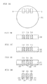
- FIGS. 2A-E schematic top view (A) and cross-sectional side view representations (B-E) are shown to illustrate an example of a method for fabricating a semiconductor chip so that it can be attached to a carrier.
- FIG. 2A shows a top view representation of a semiconductor wafer 200 comprising a plurality of processed semiconductor dies 210 .
- the semiconductor dies 210 are meant to correspond to the second semiconductor die 21 of FIGS. 1A-C .
- FIG. 2B shows a schematic cross-sectional side view representation of the semiconductor wafer 200 in a plane as indicated by line B-B.
- the semiconductor dies comprise an upper active surface having an integrated circuit incorporated therein.
- the upper surface of the semiconductor dies 210 may also comprise contact elements or contact pads which are not shown for reasons of simplicity.
- FIG. 2C shows a cross-sectional side view representation of the semiconductor wafer 200 after applying an insulating layer 220 onto the back surface of the semiconductor wafer 200 remote from the active surfaces of the semiconductor dies 210 .
- the insulating layer 220 can be made of a silicon dioxide layer obtained by a tempering process or by sputtering. Alternatively the insulating layer 220 can be made of an insulating laminate or foil. The insulating layer 220 may have a thickness in a range from 1.0 ⁇ m to 2.0 ⁇ m.
- FIG. 2D shows a cross-sectional side view representation of the semiconductor wafer 200 after applying a solder interconnect layer 230 onto the entire surface of the insulating layer 220 .
- the solder interconnect layer 230 can be made of a homogeneous layer of one and the same material or alternatively by a stack of layers of different materials.
- the solder interconnect layer 230 may have a thickness in a range from 0.5 ⁇ m to 1.0 ⁇ m.
- FIG. 2E shows a cross-sectional side view representation of separated semiconductor chips 240 obtained after singulating the semiconductor wafer 200 .
- the semiconductor chips 240 may be obtained by sawing the semiconductor wafer 200 along sawing streets.
- One possible disadvantage of the method may be the fact that in the process of sawing the semiconductor wafer 200 the solder interconnect layer 230 or particles thereof might be pulled onto or might otherwise reach the side faces of the insulating layer 220 and even the side faces of the semiconductor die 210 and thus might be able to cause leakage currents or short circuits.
- this disadvantage might be avoided.
- FIGS. 3A-C correspond to FIGS. 2A-C so that the description will not be repeated here.
- FIG. 3D shows a cross-sectional side view representation of the wafer 200 after depositing a structured solder interconnect layer 330 .
- the solder interconnect layer 330 is structured in such a way that it covers only a central portion below each one of the semiconductor dies 210 so that, as a result, a circumferential edge portion of the insulating layer 220 below each one of the semiconductor dies is not covered by the solder interconnect layer 330 .
- FIG. 3E shows again the separated semiconductor chips 340 after singulating the semiconductor wafer 200 . It can clearly be seen that the solder interconnect layer 330 is not applied onto a circumferential edge portion of the insulating layer 220 . With this measure it can be avoided that parts or particles of the solder interconnect layer 330 are conveyed or pulled onto the side faces of the insulating layer 220 or even the semiconductor die 210 .
- FIG. 4 shows a schematic cross-sectional side view representation of an electronic device according to an example.
- the electronic device 400 of FIG. 4 comprises a first carrier 410 , a second carrier 420 , a first semiconductor die 430 comprising at least one electrical contact element (not shown) on each one of two opposing main faces, and a second semiconductor die 440 comprising a first main face and a second main face opposite to the first main face and at least one electrical contact element (not shown) on the first main face.
- the first semiconductor die 430 is arranged on the first carrier 410 in such away that a first solder interconnect layer 431 is disposed between one of the main faces of the first semiconductor die 430 and the first carrier 410 .
- the second semiconductor die 440 is arranged on the second carrier 420 in such a way that an insulating layer 441 is applied onto the second main face of the second semiconductor die 440 and a second solder interconnect layer 442 is disposed between the insulating layer 441 and the second carrier 420 .
- the first and second carriers 410 and 420 and the first and second semiconductor dies 430 and 440 can be embedded in a mold material 450 . Furthermore, the first and second carriers 410 and 420 can be part of or originate from one and the same leadframe. The first and second carriers 410 and 420 and the contact elements of the first and second semiconductor dies 430 and 440 can be connected to external contact elements 460 , 470 and 480 which can be used to connect the electronic device 400 to a printed circuit board (PCB) or to any other substrate.
- PCB printed circuit board
- FIG. 4 Further examples and embodiments of the electronic device 400 of FIG. 4 can be formed along the examples and embodiments as well described above in connection with one of FIGS. 1 to 3 .
Landscapes
- Engineering & Computer Science (AREA)
- Microelectronics & Electronic Packaging (AREA)
- Power Engineering (AREA)
- Computer Hardware Design (AREA)
- Physics & Mathematics (AREA)
- Condensed Matter Physics & Semiconductors (AREA)
- General Physics & Mathematics (AREA)
- Manufacturing & Machinery (AREA)
- Internal Circuitry In Semiconductor Integrated Circuit Devices (AREA)
- Optics & Photonics (AREA)
- Die Bonding (AREA)
Abstract
Description
Claims (10)
Applications Claiming Priority (3)
| Application Number | Priority Date | Filing Date | Title |
|---|---|---|---|
| DE102014115882 | 2014-10-31 | ||
| DE102014115882.2A DE102014115882B3 (en) | 2014-10-31 | 2014-10-31 | An electronic device and a method of manufacturing an electronic device and a method of attaching a semiconductor die to a carrier |
| DE102014115882.2 | 2014-10-31 |
Publications (2)
| Publication Number | Publication Date |
|---|---|
| US20160126227A1 US20160126227A1 (en) | 2016-05-05 |
| US9881909B2 true US9881909B2 (en) | 2018-01-30 |
Family
ID=55274141
Family Applications (1)
| Application Number | Title | Priority Date | Filing Date |
|---|---|---|---|
| US14/926,892 Active US9881909B2 (en) | 2014-10-31 | 2015-10-29 | Method for attaching a semiconductor die to a carrier |
Country Status (3)
| Country | Link |
|---|---|
| US (1) | US9881909B2 (en) |
| CN (1) | CN105575827B (en) |
| DE (1) | DE102014115882B3 (en) |
Cited By (1)
| Publication number | Priority date | Publication date | Assignee | Title |
|---|---|---|---|---|
| US20190139886A1 (en) * | 2017-11-08 | 2019-05-09 | Taiwan Semiconductor Manufacturing Co., Ltd. | Package structure and manufacturing method thereof |
Families Citing this family (2)
| Publication number | Priority date | Publication date | Assignee | Title |
|---|---|---|---|---|
| US10622285B2 (en) | 2016-07-08 | 2020-04-14 | Rohm Co., Ltd. | Semiconductor device with solders of different melting points and method of manufacturing |
| EP3866187A1 (en) * | 2020-02-12 | 2021-08-18 | Infineon Technologies Austria AG | A semiconductor device comprising an embedded semiconductor die and a method for fabricating the same |
Citations (8)
| Publication number | Priority date | Publication date | Assignee | Title |
|---|---|---|---|---|
| US6306680B1 (en) * | 1999-02-22 | 2001-10-23 | General Electric Company | Power overlay chip scale packages for discrete power devices |
| US20020190317A1 (en) | 2001-06-19 | 2002-12-19 | Koninklijke Philips Electronics N.V. | Semiconductor module having multiple semiconductor chips |
| DE10149774A1 (en) | 2001-10-09 | 2003-04-24 | Bosch Gmbh Robert | Process for packing electronic modules comprises applying a power semiconductor chip on a base plate, applying a logic chip on the base plate, connecting the logic chip with the semiconductor chip, and packing the module |
| US20080173992A1 (en) | 2007-01-23 | 2008-07-24 | Infineon Technologies Ag | Semiconductor device including isolation layer |
| US20090160046A1 (en) | 2007-12-21 | 2009-06-25 | Infineon Technologies Ag | Electronic device and method |
| US20120319254A1 (en) * | 2010-03-04 | 2012-12-20 | Nec Corporation | Wiring board with built-in semiconductor element |
| CN103839842A (en) | 2012-11-19 | 2014-06-04 | 英飞凌科技股份有限公司 | Method for fabricating an electronic component |
| DE102013114059A1 (en) | 2012-12-14 | 2014-06-18 | Infineon Technologies Ag | Semiconductor component and method for its production |
-
2014
- 2014-10-31 DE DE102014115882.2A patent/DE102014115882B3/en active Active
-
2015
- 2015-10-29 US US14/926,892 patent/US9881909B2/en active Active
- 2015-10-30 CN CN201510720146.8A patent/CN105575827B/en active Active
Patent Citations (10)
| Publication number | Priority date | Publication date | Assignee | Title |
|---|---|---|---|---|
| US6306680B1 (en) * | 1999-02-22 | 2001-10-23 | General Electric Company | Power overlay chip scale packages for discrete power devices |
| US20020190317A1 (en) | 2001-06-19 | 2002-12-19 | Koninklijke Philips Electronics N.V. | Semiconductor module having multiple semiconductor chips |
| DE10149774A1 (en) | 2001-10-09 | 2003-04-24 | Bosch Gmbh Robert | Process for packing electronic modules comprises applying a power semiconductor chip on a base plate, applying a logic chip on the base plate, connecting the logic chip with the semiconductor chip, and packing the module |
| US20050006758A1 (en) | 2001-10-09 | 2005-01-13 | Kuno Wolf | Method for packaging electronic modules and multiple chip packaging |
| US20080173992A1 (en) | 2007-01-23 | 2008-07-24 | Infineon Technologies Ag | Semiconductor device including isolation layer |
| US20090160046A1 (en) | 2007-12-21 | 2009-06-25 | Infineon Technologies Ag | Electronic device and method |
| US20120319254A1 (en) * | 2010-03-04 | 2012-12-20 | Nec Corporation | Wiring board with built-in semiconductor element |
| CN103839842A (en) | 2012-11-19 | 2014-06-04 | 英飞凌科技股份有限公司 | Method for fabricating an electronic component |
| DE102013114059A1 (en) | 2012-12-14 | 2014-06-18 | Infineon Technologies Ag | Semiconductor component and method for its production |
| US20140167266A1 (en) | 2012-12-14 | 2014-06-19 | Infineon Technologies Ag | Semiconductor device having peripheral polymer structures |
Cited By (4)
| Publication number | Priority date | Publication date | Assignee | Title |
|---|---|---|---|---|
| US20190139886A1 (en) * | 2017-11-08 | 2019-05-09 | Taiwan Semiconductor Manufacturing Co., Ltd. | Package structure and manufacturing method thereof |
| US11482491B2 (en) * | 2017-11-08 | 2022-10-25 | Taiwan Semiconductor Manufacturing Company, Ltd. | Package structure with porous conductive structure and manufacturing method thereof |
| US20220367338A1 (en) * | 2017-11-08 | 2022-11-17 | Taiwan Semiconductor Manufacturing Company, Ltd. | Package structure and manufacturing method thereof |
| US11830781B2 (en) * | 2017-11-08 | 2023-11-28 | Taiwan Semiconductor Manufacturing Company, Ltd. | Package structure and manufacturing method thereof |
Also Published As
| Publication number | Publication date |
|---|---|
| CN105575827B (en) | 2018-11-02 |
| CN105575827A (en) | 2016-05-11 |
| US20160126227A1 (en) | 2016-05-05 |
| DE102014115882B3 (en) | 2016-02-25 |
Similar Documents
| Publication | Publication Date | Title |
|---|---|---|
| US11776882B2 (en) | Method of fabricating a semiconductor package | |
| US9585241B2 (en) | Substrate, chip arrangement, and method for manufacturing the same | |
| US9859251B2 (en) | Semiconductor device having a chip under package | |
| US9099454B2 (en) | Molded semiconductor package with backside die metallization | |
| US20140159054A1 (en) | Power module semiconductor device | |
| US8642389B2 (en) | Method of manufacturing a semiconductor device | |
| US8766430B2 (en) | Semiconductor modules and methods of formation thereof | |
| CN103996663A (en) | Semiconductor modules and methods of formation thereof | |
| US20200043881A1 (en) | Package structures and methods for fabricating the same | |
| US10685909B2 (en) | Power package having multiple mold compounds | |
| US20090230553A1 (en) | Semiconductor device including adhesive covered element | |
| US9806056B2 (en) | Method of packaging integrated circuits | |
| US9881909B2 (en) | Method for attaching a semiconductor die to a carrier | |
| US11598904B2 (en) | Power semiconductor module and method for producing a power semiconductor module | |
| US9171804B2 (en) | Method for fabricating an electronic component | |
| US20130264721A1 (en) | Electronic Module | |
| US9263421B2 (en) | Semiconductor device having multiple chips mounted to a carrier | |
| US9379050B2 (en) | Electronic device | |
| US10741402B2 (en) | Electronic device, electronic module and methods for fabricating the same | |
| US8970032B2 (en) | Chip module and method for fabricating a chip module | |
| US12154886B2 (en) | Semiconductor packages including electrical redistribution layers of different thicknesses and methods for manufacturing thereof | |
| US7329568B2 (en) | Method of forming active device on substrate that includes embossing insulating resin layer with metal mold | |
| US20140077388A1 (en) | Semiconductor device and method of manufacturing the same | |
| US8785248B2 (en) | Wafer level packaging using a lead-frame | |
| US10229885B2 (en) | Method of galvanic plating assisted by a current distribution layer |
Legal Events
| Date | Code | Title | Description |
|---|---|---|---|
| AS | Assignment |
Owner name: INFINEON TECHNOLOGIES AG, GERMANY Free format text: ASSIGNMENT OF ASSIGNORS INTEREST;ASSIGNORS:STUEMPFL, CHRISTIAN;HEITZER, LUDWIG;BAUER, MICHAEL;REEL/FRAME:037727/0852 Effective date: 20151030 |
|
| STCF | Information on status: patent grant |
Free format text: PATENTED CASE |
|
| CC | Certificate of correction | ||
| MAFP | Maintenance fee payment |
Free format text: PAYMENT OF MAINTENANCE FEE, 4TH YEAR, LARGE ENTITY (ORIGINAL EVENT CODE: M1551); ENTITY STATUS OF PATENT OWNER: LARGE ENTITY Year of fee payment: 4 |
|
| MAFP | Maintenance fee payment |
Free format text: PAYMENT OF MAINTENANCE FEE, 8TH YEAR, LARGE ENTITY (ORIGINAL EVENT CODE: M1552); ENTITY STATUS OF PATENT OWNER: LARGE ENTITY Year of fee payment: 8 |