US9881785B2 - Method of preventing charge accumulation in manufacture of semiconductor device - Google Patents
Method of preventing charge accumulation in manufacture of semiconductor device Download PDFInfo
- Publication number
- US9881785B2 US9881785B2 US13/783,466 US201313783466A US9881785B2 US 9881785 B2 US9881785 B2 US 9881785B2 US 201313783466 A US201313783466 A US 201313783466A US 9881785 B2 US9881785 B2 US 9881785B2
- Authority
- US
- United States
- Prior art keywords
- material layer
- layer
- substrate
- graphene
- forming
- Prior art date
- Legal status (The legal status is an assumption and is not a legal conclusion. Google has not performed a legal analysis and makes no representation as to the accuracy of the status listed.)
- Active
Links
- 238000000034 method Methods 0.000 title claims abstract description 37
- 239000004065 semiconductor Substances 0.000 title claims abstract description 19
- 238000004519 manufacturing process Methods 0.000 title claims abstract description 17
- 238000009825 accumulation Methods 0.000 title claims abstract description 16
- 239000000463 material Substances 0.000 claims abstract description 64
- OKTJSMMVPCPJKN-UHFFFAOYSA-N Carbon Chemical compound [C] OKTJSMMVPCPJKN-UHFFFAOYSA-N 0.000 claims abstract description 52
- 229910021389 graphene Inorganic materials 0.000 claims abstract description 52
- 239000000758 substrate Substances 0.000 claims abstract description 39
- 238000000059 patterning Methods 0.000 claims abstract description 11
- 238000009413 insulation Methods 0.000 claims abstract description 4
- 239000002904 solvent Substances 0.000 claims description 11
- 238000010884 ion-beam technique Methods 0.000 claims description 6
- 238000010894 electron beam technology Methods 0.000 claims description 5
- 239000011248 coating agent Substances 0.000 claims description 4
- 238000000576 coating method Methods 0.000 claims description 4
- 229910052581 Si3N4 Inorganic materials 0.000 claims description 3
- VYPSYNLAJGMNEJ-UHFFFAOYSA-N Silicium dioxide Chemical compound O=[Si]=O VYPSYNLAJGMNEJ-UHFFFAOYSA-N 0.000 claims description 3
- HQVNEWCFYHHQES-UHFFFAOYSA-N silicon nitride Chemical compound N12[Si]34N5[Si]62N3[Si]51N64 HQVNEWCFYHHQES-UHFFFAOYSA-N 0.000 claims description 3
- 229910052814 silicon oxide Inorganic materials 0.000 claims description 3
- 239000010410 layer Substances 0.000 description 92
- 239000013077 target material Substances 0.000 description 8
- 229910052751 metal Inorganic materials 0.000 description 7
- 239000002184 metal Substances 0.000 description 7
- 230000006378 damage Effects 0.000 description 5
- 239000010409 thin film Substances 0.000 description 5
- 239000002356 single layer Substances 0.000 description 4
- ZMXDDKWLCZADIW-UHFFFAOYSA-N N,N-Dimethylformamide Chemical compound CN(C)C=O ZMXDDKWLCZADIW-UHFFFAOYSA-N 0.000 description 3
- 238000005229 chemical vapour deposition Methods 0.000 description 2
- 238000000151 deposition Methods 0.000 description 2
- 230000005684 electric field Effects 0.000 description 2
- 238000000609 electron-beam lithography Methods 0.000 description 2
- 238000004321 preservation Methods 0.000 description 2
- SECXISVLQFMRJM-UHFFFAOYSA-N N-Methylpyrrolidone Chemical compound CN1CCCC1=O SECXISVLQFMRJM-UHFFFAOYSA-N 0.000 description 1
- 239000002322 conducting polymer Substances 0.000 description 1
- 229920001940 conductive polymer Polymers 0.000 description 1
- 230000008021 deposition Effects 0.000 description 1
- 230000006866 deterioration Effects 0.000 description 1
- 230000000694 effects Effects 0.000 description 1
- PCHJSUWPFVWCPO-UHFFFAOYSA-N gold Chemical compound [Au] PCHJSUWPFVWCPO-UHFFFAOYSA-N 0.000 description 1
- 229910052737 gold Inorganic materials 0.000 description 1
- 239000010931 gold Substances 0.000 description 1
- 229910000510 noble metal Inorganic materials 0.000 description 1
- 230000009257 reactivity Effects 0.000 description 1
- 230000007261 regionalization Effects 0.000 description 1
- 229910052594 sapphire Inorganic materials 0.000 description 1
- 239000010980 sapphire Substances 0.000 description 1
- 229910052709 silver Inorganic materials 0.000 description 1
- 239000004332 silver Substances 0.000 description 1
Images


Classifications
-
- H—ELECTRICITY
- H01—ELECTRIC ELEMENTS
- H01L—SEMICONDUCTOR DEVICES NOT COVERED BY CLASS H10
- H01L21/00—Processes or apparatus adapted for the manufacture or treatment of semiconductor or solid state devices or of parts thereof
- H01L21/02—Manufacture or treatment of semiconductor devices or of parts thereof
- H01L21/02104—Forming layers
- H01L21/02107—Forming insulating materials on a substrate
- H01L21/02109—Forming insulating materials on a substrate characterised by the type of layer, e.g. type of material, porous/non-porous, pre-cursors, mixtures or laminates
- H01L21/02112—Forming insulating materials on a substrate characterised by the type of layer, e.g. type of material, porous/non-porous, pre-cursors, mixtures or laminates characterised by the material of the layer
- H01L21/02115—Forming insulating materials on a substrate characterised by the type of layer, e.g. type of material, porous/non-porous, pre-cursors, mixtures or laminates characterised by the material of the layer the material being carbon, e.g. alpha-C, diamond or hydrogen doped carbon
-
- H—ELECTRICITY
- H01—ELECTRIC ELEMENTS
- H01J—ELECTRIC DISCHARGE TUBES OR DISCHARGE LAMPS
- H01J37/00—Discharge tubes with provision for introducing objects or material to be exposed to the discharge, e.g. for the purpose of examination or processing thereof
- H01J37/02—Details
- H01J37/026—Means for avoiding or neutralising unwanted electrical charges on tube components
-
- H—ELECTRICITY
- H01—ELECTRIC ELEMENTS
- H01J—ELECTRIC DISCHARGE TUBES OR DISCHARGE LAMPS
- H01J37/00—Discharge tubes with provision for introducing objects or material to be exposed to the discharge, e.g. for the purpose of examination or processing thereof
- H01J37/30—Electron-beam or ion-beam tubes for localised treatment of objects
- H01J37/317—Electron-beam or ion-beam tubes for localised treatment of objects for changing properties of the objects or for applying thin layers thereon, e.g. for ion implantation
- H01J37/3174—Particle-beam lithography, e.g. electron beam lithography
-
- H—ELECTRICITY
- H01—ELECTRIC ELEMENTS
- H01L—SEMICONDUCTOR DEVICES NOT COVERED BY CLASS H10
- H01L21/00—Processes or apparatus adapted for the manufacture or treatment of semiconductor or solid state devices or of parts thereof
- H01L21/02—Manufacture or treatment of semiconductor devices or of parts thereof
- H01L21/027—Making masks on semiconductor bodies for further photolithographic processing not provided for in group H01L21/18 or H01L21/34
- H01L21/0271—Making masks on semiconductor bodies for further photolithographic processing not provided for in group H01L21/18 or H01L21/34 comprising organic layers
- H01L21/0273—Making masks on semiconductor bodies for further photolithographic processing not provided for in group H01L21/18 or H01L21/34 comprising organic layers characterised by the treatment of photoresist layers
- H01L21/0274—Photolithographic processes
- H01L21/0275—Photolithographic processes using lasers
-
- H—ELECTRICITY
- H01—ELECTRIC ELEMENTS
- H01L—SEMICONDUCTOR DEVICES NOT COVERED BY CLASS H10
- H01L21/00—Processes or apparatus adapted for the manufacture or treatment of semiconductor or solid state devices or of parts thereof
- H01L21/02—Manufacture or treatment of semiconductor devices or of parts thereof
- H01L21/04—Manufacture or treatment of semiconductor devices or of parts thereof the devices having potential barriers, e.g. a PN junction, depletion layer or carrier concentration layer
- H01L21/18—Manufacture or treatment of semiconductor devices or of parts thereof the devices having potential barriers, e.g. a PN junction, depletion layer or carrier concentration layer the devices having semiconductor bodies comprising elements of Group IV of the Periodic Table or AIIIBV compounds with or without impurities, e.g. doping materials
- H01L21/26—Bombardment with radiation
- H01L21/263—Bombardment with radiation with high-energy radiation
- H01L21/2633—Bombardment with radiation with high-energy radiation for etching, e.g. sputteretching
-
- H—ELECTRICITY
- H01—ELECTRIC ELEMENTS
- H01L—SEMICONDUCTOR DEVICES NOT COVERED BY CLASS H10
- H01L21/00—Processes or apparatus adapted for the manufacture or treatment of semiconductor or solid state devices or of parts thereof
- H01L21/02—Manufacture or treatment of semiconductor devices or of parts thereof
- H01L21/04—Manufacture or treatment of semiconductor devices or of parts thereof the devices having potential barriers, e.g. a PN junction, depletion layer or carrier concentration layer
- H01L21/18—Manufacture or treatment of semiconductor devices or of parts thereof the devices having potential barriers, e.g. a PN junction, depletion layer or carrier concentration layer the devices having semiconductor bodies comprising elements of Group IV of the Periodic Table or AIIIBV compounds with or without impurities, e.g. doping materials
- H01L21/28—Manufacture of electrodes on semiconductor bodies using processes or apparatus not provided for in groups H01L21/20 - H01L21/268
- H01L21/28008—Making conductor-insulator-semiconductor electrodes
- H01L21/28017—Making conductor-insulator-semiconductor electrodes the insulator being formed after the semiconductor body, the semiconductor being silicon
- H01L21/28026—Making conductor-insulator-semiconductor electrodes the insulator being formed after the semiconductor body, the semiconductor being silicon characterised by the conductor
- H01L21/28123—Lithography-related aspects, e.g. sub-lithography lengths; Isolation-related aspects, e.g. to solve problems arising at the crossing with the side of the device isolation; Planarisation aspects
-
- H—ELECTRICITY
- H01—ELECTRIC ELEMENTS
- H01L—SEMICONDUCTOR DEVICES NOT COVERED BY CLASS H10
- H01L21/00—Processes or apparatus adapted for the manufacture or treatment of semiconductor or solid state devices or of parts thereof
- H01L21/02—Manufacture or treatment of semiconductor devices or of parts thereof
- H01L21/04—Manufacture or treatment of semiconductor devices or of parts thereof the devices having potential barriers, e.g. a PN junction, depletion layer or carrier concentration layer
- H01L21/18—Manufacture or treatment of semiconductor devices or of parts thereof the devices having potential barriers, e.g. a PN junction, depletion layer or carrier concentration layer the devices having semiconductor bodies comprising elements of Group IV of the Periodic Table or AIIIBV compounds with or without impurities, e.g. doping materials
- H01L21/30—Treatment of semiconductor bodies using processes or apparatus not provided for in groups H01L21/20 - H01L21/26
- H01L21/31—Treatment of semiconductor bodies using processes or apparatus not provided for in groups H01L21/20 - H01L21/26 to form insulating layers thereon, e.g. for masking or by using photolithographic techniques; After treatment of these layers; Selection of materials for these layers
- H01L21/3105—After-treatment
- H01L21/311—Etching the insulating layers by chemical or physical means
- H01L21/31105—Etching inorganic layers
-
- H—ELECTRICITY
- H01—ELECTRIC ELEMENTS
- H01L—SEMICONDUCTOR DEVICES NOT COVERED BY CLASS H10
- H01L21/00—Processes or apparatus adapted for the manufacture or treatment of semiconductor or solid state devices or of parts thereof
- H01L21/70—Manufacture or treatment of devices consisting of a plurality of solid state components formed in or on a common substrate or of parts thereof; Manufacture of integrated circuit devices or of parts thereof
- H01L21/77—Manufacture or treatment of devices consisting of a plurality of solid state components or integrated circuits formed in, or on, a common substrate
- H01L21/78—Manufacture or treatment of devices consisting of a plurality of solid state components or integrated circuits formed in, or on, a common substrate with subsequent division of the substrate into plural individual devices
- H01L21/82—Manufacture or treatment of devices consisting of a plurality of solid state components or integrated circuits formed in, or on, a common substrate with subsequent division of the substrate into plural individual devices to produce devices, e.g. integrated circuits, each consisting of a plurality of components
-
- H—ELECTRICITY
- H01—ELECTRIC ELEMENTS
- H01J—ELECTRIC DISCHARGE TUBES OR DISCHARGE LAMPS
- H01J2237/00—Discharge tubes exposing object to beam, e.g. for analysis treatment, etching, imaging
- H01J2237/004—Charge control of objects or beams
- H01J2237/0041—Neutralising arrangements
-
- H—ELECTRICITY
- H01—ELECTRIC ELEMENTS
- H01J—ELECTRIC DISCHARGE TUBES OR DISCHARGE LAMPS
- H01J2237/00—Discharge tubes exposing object to beam, e.g. for analysis treatment, etching, imaging
- H01J2237/30—Electron or ion beam tubes for processing objects
- H01J2237/317—Processing objects on a microscale
- H01J2237/3174—Etching microareas
Definitions
- Apparatuses and methods consistent with exemplary embodiments relate to the manufacture of a semiconductor device, and more particularly, to a method of preventing a charge accumulation by using a graphene layer in the manufacture of a semiconductor device.
- a metal thin film may be formed on the surface of the target material layer to overcome the above problem.
- the metal thin film formed on the surface of the target material layer may damage a substrate and may damage a previously formed pattern.
- the metal thin film may operate as an obstacle in transferring a previously formed pattern to the substrate.
- a noble metal such as gold or silver is used as the metal thin film.
- the whole manufacturing cost increases.
- a product using a conducting polymer is introduced to improve such a shortcoming, but has a problem in that a preservation period is short and a change in quality may occur in specific conditions. For example, a residue may form due to deterioration in the FIB process.
- One or more exemplary embodiments may provide methods of preventing a charge accumulation, which may prevent the damage of a target material layer or a distortion of a pattern during the manufacturing process of a semiconductor device.
- a method of preventing a charge accumulation in the manufacturing process of a semiconductor device includes: forming a material layer on a substrate; and patterning the material layer, wherein a graphene layer is formed under or on the material layer before patterning the material layer.
- the substrate may be an insulation substrate.
- the substrate may have a stacked structure including a plurality of layers.
- the material layer may include a silicon oxide layer, a silicon nitride layer, or an insulating layer that is capable of being patterned by using an electron beam or a focused ion beam (FIB).
- FIB focused ion beam
- the graphene layer may include a single layer or a plurality of layers.
- the graphene layer may be formed only on a portion between the substrate and the material layer.
- the graphene layer may be formed only on a portion of an upper surface of the material layer.
- a process of forming the graphene layer may include: coating a solvent, including graphene flakes, on a surface of the material layer, on which the graphene layer is to be formed; and baking a resultant structure on which the solvent has been coated.
- a method of preventing a charge accumulation in the manufacturing process of a semiconductor device includes forming a graphene layer on or under a target material layer.
- the graphene layer has conductivity of a metal level and has a very thin structure, and thus does not operate as an obstacle when transferring a pattern thereof.
- the graphene layer may be easily removed by using plasma or the like, has a long preservation period, hardly deteriorates, and has a low reactivity with a different material.
- the graphene layer when a great number of electric charges are applied to a target material layer, a charge accumulation on the surface of the target material layer may be prevented and another path of electric charges may be provided. Accordingly, a distortion of a material layer pattern and the damage or destruction of a material layer pattern, which occur when using electron beam lithography or a focused Ion beam (FIB), may be prevented.
- the graphene layer may be used in electromagnetic wave shielding and protection for a structure against a strong electric field.
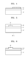
- FIG. 1 is a cross-sectional view illustrating a method of preventing a charge accumulation in the manufacturing process of a semiconductor device, according to an exemplary embodiment
- FIG. 2 is a cross-sectional view illustrating a case in which a graphene layer is formed only on a portion of an upper surface of a substrate;
- FIG. 3 is a cross-sectional view illustrating a method of preventing a charge accumulation in the manufacturing process of a semiconductor device, according to an exemplary embodiment
- FIG. 4 is a cross-sectional view illustrating a case in which a graphene layer is formed only on a portion of an upper surface of a material layer
- FIGS. 5 and 6 are cross-sectional views illustrating a method of preventing a charge accumulation in the manufacturing process of a semiconductor device, according to an exemplary embodiment.
- FIG. 1 is a cross-sectional view illustrating a method of preventing a charge accumulation in the manufacturing process of a semiconductor device.
- a graphene layer 22 is formed on the upper surface of a substrate 20 .
- the graphene layer 22 may be formed separately from the substrate 20 .
- the graphene layer 22 may be formed in a location separate from the substrate 20 , and may then be transferred to the upper surface of the substrate 20 .
- the graphene layer 22 may be formed by chemical vapor deposition (CVD) and may then be transferred to the upper surface of the substrate 20 .
- CVD chemical vapor deposition
- the substrate 20 may have the effect of having permanent conductivity.
- the graphene layer 22 may be a single layer or may be multiple layers.
- the graphene layer 22 may have a stacked form in which a plurality of single layers are stacked.
- a material layer 24 is formed on the graphene layer 22 .
- the material layer 24 is a layer that is to be patterned or processed by using an electron beam or a focused ion beam (FIB).
- the material layer 24 may be an insulating layer, and may be, for example, a silicon oxide layer or a silicon nitride layer. If the material layer 24 is not a material having conductivity, the material layer 24 may be any material layer that may be patterned by using the electron beam or a FIB.
- the graphene layer 22 may be formed over the entirety of the whole upper surface of the substrate 20 . However, as illustrated in FIG. 2 , the graphene layer 22 may alternately be formed on only a portion of the upper surface of the substrate 20 . Due to the conductivity of the graphene layer 22 , it is important that the graphene layer 22 exists, but the graphene layer 22 may be formed on the entirety of the whole upper surface of the substrate 20 or only on a portion of the upper surface of the substrate 20 .
- a semiconductor device may be formed by depositing material layers constituting the semiconductor device.
- a transistor may be formed by performing a process of forming a gate deposition material, and a process of forming a source and a drain.
- FIG. 3 is a cross-sectional view illustrating a method of preventing a charge accumulation in the manufacturing process of a semiconductor device. Like reference numerals are used with respect to elements that are the same as those illustrated in FIG. 1 , and descriptions of the same elements are omitted.
- a material layer 24 is formed on a substrate 30 .
- a graphene layer 22 is formed on the upper surface of the material layer 24 .
- the substrate 30 may be an insulation substrate, and, for example, may be a sapphire substrate.
- the graphene layer 22 is formed to cover the whole upper surface of the material layer 24 .
- the graphene layer 22 may be formed only on a portion of the upper surface of the material layer 24 . The reason for this is the same as that described with reference to FIG. 2 .
- the substrate 30 has no conductivity.
- FIG. 3 and FIG. 4 may be applied to a case where a temporary surface conductivity is needed.
- FIG. 5 is a cross-sectional view illustrating a method of preventing a charge accumulation in the manufacturing process of a semiconductor device. Like reference numerals are used with respect to elements that are the same as those illustrated in FIG. 1 , and descriptions of the same elements are omitted.
- a material layer 24 is formed on a substrate 30 .
- a material pattern 46 may be formed on the material layer 24 .
- the material pattern 46 may be an insulating pattern.
- the material pattern 46 may be a portion of the material layer 24 .
- a graphene layer may be formed by using a method that is different from a method of transferring a graphene layer, which is used in the cases of FIG. 1 and FIG. 3 .
- a solvent 40 covering the material pattern 46 is coated on the material layer 24 .
- the solvent 40 may include graphene flakes.
- dimethylformamide or N-methylpyrrolidone may be used as the solvent 40 .
- the size of the graphene flakes included in the solvent 40 may be, for example, in the range of about 10 nm to about 10 um.
- a resultant structure on which the solvent 40 has been coated is baked.
- the baking of the resultant structure may be performed at a predetermined temperature, and, for example, may be performed in the range of about 110° C. to about 140° C.
- a graphene layer 40 A is formed on the upper surface of the material layer 24 as illustrated in FIG. 6 .
- the material layer 24 is patterned to achieve a desired form.
- the graphene layer 40 A may also be patterned together with the material layer 24 .
- the graphene layer 40 A described with reference to FIGS. 5 and 6 may be used as the graphene layer 22 of FIG. 1 .
- FIGS. 5 and 6 may be applied to also a case where a concave portion exists in the material layer 24 .
- a uniform graphene layer may be formed also on an uneven portion.
- the substrate 20 or 30 may be simply a substrate including a single layer. However, the substrate 20 or 30 may be a lower structure of a semiconductor device, which includes a stacked structure having a plurality of layers.
Landscapes
- Engineering & Computer Science (AREA)
- Physics & Mathematics (AREA)
- Condensed Matter Physics & Semiconductors (AREA)
- General Physics & Mathematics (AREA)
- Manufacturing & Machinery (AREA)
- Computer Hardware Design (AREA)
- Microelectronics & Electronic Packaging (AREA)
- Power Engineering (AREA)
- High Energy & Nuclear Physics (AREA)
- Chemical & Material Sciences (AREA)
- Health & Medical Sciences (AREA)
- Toxicology (AREA)
- Inorganic Chemistry (AREA)
- Analytical Chemistry (AREA)
- Optics & Photonics (AREA)
- Carbon And Carbon Compounds (AREA)
Abstract
A method of preventing a charge accumulation in the manufacturing process of a semiconductor device is provided. The method includes: forming a material layer on a substrate; patterning (or processing) the material layer; and forming a graphene layer before patterning the material layer, wherein the graphene layer is formed on a surface of the material layer or on a surface of the substrate under the material layer. The substrate may be an insulation substrate. In addition, the substrate may have a stacked structure including a plurality of layers.
Description
This application claims priority from Korean Patent Application No. 10-2012-0091469, filed on Aug. 21, 2012, in the Korean Intellectual Property Office, the disclosure of which is incorporated herein in its entirety by reference.
Field
Apparatuses and methods consistent with exemplary embodiments relate to the manufacture of a semiconductor device, and more particularly, to a method of preventing a charge accumulation by using a graphene layer in the manufacture of a semiconductor device.
Description of the Related Art
In an object that is placed in a strong electric field or an object to which a great number of electric charges are applied, electric charges are distributed on the surface thereof unless the object is not a metal, and thus, the progress of subsequent processes may be disturbed.
In a process, which uses electron beam lithography or a focused ion beam (FIB), it is fundamental to process a desired structure by applying a great number of electric charges thereto. However, when accumulated electric charges exist in a target material layer, the pattern formation and processing for the target material layer may be distorted.
A metal thin film may be formed on the surface of the target material layer to overcome the above problem. However, the metal thin film formed on the surface of the target material layer may damage a substrate and may damage a previously formed pattern. In addition, the metal thin film may operate as an obstacle in transferring a previously formed pattern to the substrate.
To secure conductivity of the metal thin film, a noble metal such as gold or silver is used as the metal thin film. However, in this case, the whole manufacturing cost increases.
A product using a conducting polymer is introduced to improve such a shortcoming, but has a problem in that a preservation period is short and a change in quality may occur in specific conditions. For example, a residue may form due to deterioration in the FIB process.
One or more exemplary embodiments may provide methods of preventing a charge accumulation, which may prevent the damage of a target material layer or a distortion of a pattern during the manufacturing process of a semiconductor device.
Additional exemplary aspects and advantages will be set forth in part in the description which follows and, in part, will be apparent from the description, or may be learned by practice of the presented embodiments.
According to an aspect of an exemplary embodiment, a method of preventing a charge accumulation in the manufacturing process of a semiconductor device includes: forming a material layer on a substrate; and patterning the material layer, wherein a graphene layer is formed under or on the material layer before patterning the material layer.
The substrate may be an insulation substrate. In addition, the substrate may have a stacked structure including a plurality of layers.
The material layer may include a silicon oxide layer, a silicon nitride layer, or an insulating layer that is capable of being patterned by using an electron beam or a focused ion beam (FIB).
The graphene layer may include a single layer or a plurality of layers.
The graphene layer may be formed only on a portion between the substrate and the material layer. The graphene layer may be formed only on a portion of an upper surface of the material layer.
A process of forming the graphene layer may include: coating a solvent, including graphene flakes, on a surface of the material layer, on which the graphene layer is to be formed; and baking a resultant structure on which the solvent has been coated.
According to an aspect of another exemplary embodiment, a method of preventing a charge accumulation in the manufacturing process of a semiconductor device includes forming a graphene layer on or under a target material layer. The graphene layer has conductivity of a metal level and has a very thin structure, and thus does not operate as an obstacle when transferring a pattern thereof. In addition, the graphene layer may be easily removed by using plasma or the like, has a long preservation period, hardly deteriorates, and has a low reactivity with a different material.
By using such a graphene layer, when a great number of electric charges are applied to a target material layer, a charge accumulation on the surface of the target material layer may be prevented and another path of electric charges may be provided. Accordingly, a distortion of a material layer pattern and the damage or destruction of a material layer pattern, which occur when using electron beam lithography or a focused Ion beam (FIB), may be prevented. In addition, the graphene layer may be used in electromagnetic wave shielding and protection for a structure against a strong electric field.
These and/or other exemplary aspects and advantages will become apparent and more readily appreciated from the following description of exemplary embodiments, taken in conjunction with the accompanying drawings in which:
A method of preventing a charge accumulation in the manufacturing process of a semiconductor device, according to an exemplary embodiment, will now be described in detail with reference to the accompanying drawings. In the drawings, thicknesses of layers and regions may be exaggerated for clarity.
Referring to FIG. 1 , a graphene layer 22 is formed on the upper surface of a substrate 20. The graphene layer 22 may be formed separately from the substrate 20. In other words, the graphene layer 22 may be formed in a location separate from the substrate 20, and may then be transferred to the upper surface of the substrate 20. For example, the graphene layer 22 may be formed by chemical vapor deposition (CVD) and may then be transferred to the upper surface of the substrate 20. After the graphene layer 22 is disposed on the substrate 20, the substrate 20 may have the effect of having permanent conductivity. The graphene layer 22 may be a single layer or may be multiple layers. In the case where the graphene layer 22 includes multiple layers, the graphene layer 22 may have a stacked form in which a plurality of single layers are stacked. A material layer 24 is formed on the graphene layer 22. The material layer 24 is a layer that is to be patterned or processed by using an electron beam or a focused ion beam (FIB). The material layer 24 may be an insulating layer, and may be, for example, a silicon oxide layer or a silicon nitride layer. If the material layer 24 is not a material having conductivity, the material layer 24 may be any material layer that may be patterned by using the electron beam or a FIB.
The graphene layer 22 may be formed over the entirety of the whole upper surface of the substrate 20. However, as illustrated in FIG. 2 , the graphene layer 22 may alternately be formed on only a portion of the upper surface of the substrate 20. Due to the conductivity of the graphene layer 22, it is important that the graphene layer 22 exists, but the graphene layer 22 may be formed on the entirety of the whole upper surface of the substrate 20 or only on a portion of the upper surface of the substrate 20.
In FIG. 1 or FIG. 2 , after performing a patterning process with respect to the material layer 24, a semiconductor device may be formed by depositing material layers constituting the semiconductor device. For example, a transistor may be formed by performing a process of forming a gate deposition material, and a process of forming a source and a drain.
Referring to FIG. 3 , a material layer 24 is formed on a substrate 30. A graphene layer 22 is formed on the upper surface of the material layer 24. The substrate 30 may be an insulation substrate, and, for example, may be a sapphire substrate.
In FIG. 3 , the graphene layer 22 is formed to cover the whole upper surface of the material layer 24. However, as illustrated in FIG. 4 , the graphene layer 22 may be formed only on a portion of the upper surface of the material layer 24. The reason for this is the same as that described with reference to FIG. 2 .
As in FIG. 3 and FIG. 4 , in the case where the graphene layer 22 is directly formed on the upper surface of the material layer 24, the substrate 30 has no conductivity.
The cases of FIG. 3 and FIG. 4 may be applied to a case where a temporary surface conductivity is needed.
Referring to FIG. 5 , a material layer 24 is formed on a substrate 30. A material pattern 46 may be formed on the material layer 24. The material pattern 46 may be an insulating pattern. The material pattern 46 may be a portion of the material layer 24. When, in this manner, a convex portion such as the material pattern 46, that is, a ridge portion exists on the flat material layer 24, a graphene layer may be formed by using a method that is different from a method of transferring a graphene layer, which is used in the cases of FIG. 1 and FIG. 3 .
For example, as illustrated in FIG. 5 , a solvent 40 covering the material pattern 46 is coated on the material layer 24. The solvent 40 may include graphene flakes. For example, dimethylformamide or N-methylpyrrolidone may be used as the solvent 40. The size of the graphene flakes included in the solvent 40 may be, for example, in the range of about 10 nm to about 10 um.
After coating the solvent 40, a resultant structure on which the solvent 40 has been coated is baked. The baking of the resultant structure may be performed at a predetermined temperature, and, for example, may be performed in the range of about 110° C. to about 140° C.
By the baking, a graphene layer 40A is formed on the upper surface of the material layer 24 as illustrated in FIG. 6 . After forming the graphene layer 40A, the material layer 24 is patterned to achieve a desired form. In this case, the graphene layer 40A may also be patterned together with the material layer 24.
The graphene layer 40A described with reference to FIGS. 5 and 6 may be used as the graphene layer 22 of FIG. 1 .
The method illustrated in FIGS. 5 and 6 may be applied to also a case where a concave portion exists in the material layer 24.
Since the method illustrated in FIGS. 5 and 6 uses a solvent coating, a uniform graphene layer may be formed also on an uneven portion.
In FIGS. 1 through 6 , the substrate 20 or 30 may be simply a substrate including a single layer. However, the substrate 20 or 30 may be a lower structure of a semiconductor device, which includes a stacked structure having a plurality of layers.
It should be understood that the exemplary embodiments described herein should be considered in a descriptive sense only and not for purposes of limitation. Descriptions of features or aspects within each embodiment should typically be considered as available for other similar features or aspects in other embodiments.
Claims (7)
1. A method of preventing a charge accumulation in a manufacturing process of a semiconductor device, the method comprising:
forming a material layer on a substrate;
after forming the material layer, forming a graphene layer on the material layer; and
patterning the material layer,
wherein a convex portion is formed on the material layer and the convex portion is covered with the graphene layer.
2. The method of claim 1 , wherein the substrate is an insulation substrate.
3. The method of claim 1 , wherein the substrate has a stacked structure comprising a plurality of layers.
4. The method of claim 1 , wherein the material layer comprises one of a silicon oxide layer, a silicon nitride layer, and an insulating layer, and the patterning the material layer comprises patterning the material layer by using one of an electron beam and a focused ion beam.
5. The method of claim 1 , wherein a process of forming the graphene layer comprises:
coating a solvent comprising graphene flakes on a surface of the material layer; and
baking a resultant structure including the coated solvent.
6. The method of claim 1 , wherein the patterning the material layer comprises patterning the material layer using one of an electron beam and a focused ion beam.
7. A method of preventing a charge accumulation in a manufacturing process of a semiconductor device, the method comprising:
forming a material layer on a substrate;
after forming the material layer, forming a graphene layer on the material layer; and
patterning the material layer,
wherein a convex portion is formed on the material layer, the convex portion is covered with the graphene layer and the forming the material layer on the substrate and the forming the graphene layer on the material layer are sequentially performed.
Applications Claiming Priority (2)
| Application Number | Priority Date | Filing Date | Title |
|---|---|---|---|
| KR10-2012-0091469 | 2012-08-21 | ||
| KR1020120091469A KR101920722B1 (en) | 2012-08-21 | 2012-08-21 | Method of preventing charge accumulation in manufacture of semiconductor device |
Publications (2)
| Publication Number | Publication Date |
|---|---|
| US20140057451A1 US20140057451A1 (en) | 2014-02-27 |
| US9881785B2 true US9881785B2 (en) | 2018-01-30 |
Family
ID=50148359
Family Applications (1)
| Application Number | Title | Priority Date | Filing Date |
|---|---|---|---|
| US13/783,466 Active US9881785B2 (en) | 2012-08-21 | 2013-03-04 | Method of preventing charge accumulation in manufacture of semiconductor device |
Country Status (2)
| Country | Link |
|---|---|
| US (1) | US9881785B2 (en) |
| KR (1) | KR101920722B1 (en) |
Families Citing this family (1)
| Publication number | Priority date | Publication date | Assignee | Title |
|---|---|---|---|---|
| US10950485B2 (en) * | 2019-04-17 | 2021-03-16 | Taiwan Semiconductor Manufacturing Co., Ltd. | Semiconductor processing apparatus and method utilizing electrostatic discharge (ESD) prevention layer |
Citations (8)
| Publication number | Priority date | Publication date | Assignee | Title |
|---|---|---|---|---|
| US6586158B2 (en) | 2001-05-25 | 2003-07-01 | The United States Of America As Represented By The Secretary Of The Navy | Anti-charging layer for beam lithography and mask fabrication |
| US20060272796A1 (en) | 2001-04-04 | 2006-12-07 | Asmussen Erick R | Flexible graphite flooring heat spreader |
| US20070284557A1 (en) | 2006-06-13 | 2007-12-13 | Unidym, Inc. | Graphene film as transparent and electrically conducting material |
| US20090155578A1 (en) | 2007-12-17 | 2009-06-18 | Aruna Zhamu | Nano-scaled graphene platelets with a high length-to-width aspect ratio |
| US20100295023A1 (en) * | 2009-04-06 | 2010-11-25 | Purdue Research Foundation | Field effect transistor fabrication from carbon nanotubes |
| JP2011063492A (en) | 2009-09-18 | 2011-03-31 | Fuji Electric Holdings Co Ltd | Method for producing graphene thin film, and graphene thin film |
| US20110121409A1 (en) * | 2009-11-23 | 2011-05-26 | Samsung Electronics Co., Ltd. | Field effect transistors, methods of fabricating a carbon-insulating layer using molecular beam epitaxy and methods of fabricating a field effect transistor |
| US20140048799A1 (en) * | 2011-02-16 | 2014-02-20 | William Marsh Rice University | Invisible/transparent nonvolatile memory |
-
2012
- 2012-08-21 KR KR1020120091469A patent/KR101920722B1/en active IP Right Grant
-
2013
- 2013-03-04 US US13/783,466 patent/US9881785B2/en active Active
Patent Citations (9)
| Publication number | Priority date | Publication date | Assignee | Title |
|---|---|---|---|---|
| US20060272796A1 (en) | 2001-04-04 | 2006-12-07 | Asmussen Erick R | Flexible graphite flooring heat spreader |
| US6586158B2 (en) | 2001-05-25 | 2003-07-01 | The United States Of America As Represented By The Secretary Of The Navy | Anti-charging layer for beam lithography and mask fabrication |
| US6773865B2 (en) | 2001-05-25 | 2004-08-10 | The United States Of America As Represented By The Secretary Of The Navy | Anti-charging layer for beam lithography and mask fabrication |
| US20070284557A1 (en) | 2006-06-13 | 2007-12-13 | Unidym, Inc. | Graphene film as transparent and electrically conducting material |
| US20090155578A1 (en) | 2007-12-17 | 2009-06-18 | Aruna Zhamu | Nano-scaled graphene platelets with a high length-to-width aspect ratio |
| US20100295023A1 (en) * | 2009-04-06 | 2010-11-25 | Purdue Research Foundation | Field effect transistor fabrication from carbon nanotubes |
| JP2011063492A (en) | 2009-09-18 | 2011-03-31 | Fuji Electric Holdings Co Ltd | Method for producing graphene thin film, and graphene thin film |
| US20110121409A1 (en) * | 2009-11-23 | 2011-05-26 | Samsung Electronics Co., Ltd. | Field effect transistors, methods of fabricating a carbon-insulating layer using molecular beam epitaxy and methods of fabricating a field effect transistor |
| US20140048799A1 (en) * | 2011-02-16 | 2014-02-20 | William Marsh Rice University | Invisible/transparent nonvolatile memory |
Also Published As
| Publication number | Publication date |
|---|---|
| KR101920722B1 (en) | 2018-11-21 |
| KR20140025158A (en) | 2014-03-04 |
| US20140057451A1 (en) | 2014-02-27 |
Similar Documents
| Publication | Publication Date | Title |
|---|---|---|
| US8728880B2 (en) | Graphene electronic device and method of fabricating the same | |
| US9159907B2 (en) | Hybrid film for protecting MTJ stacks of MRAM | |
| WO2018014371A1 (en) | Flexible array substrate and preparation method therefor, and flexible display device | |
| CN109616587B (en) | Display substrate, manufacturing method thereof and display device | |
| KR20140037808A (en) | Method for fabricating array substrate, array substrate and display device | |
| CN109166862B (en) | Flexible OLED display panel and preparation method thereof | |
| US10083988B2 (en) | Complementary thin film transistor and manufacturing method thereof, array substrate, display apparatus | |
| US9240353B2 (en) | Method for manufacturing array substrate by forming common electrode connecting NMOS in display area and PMOS in drive area | |
| CN108231553B (en) | Manufacturing method of thin film transistor and manufacturing method of array substrate | |
| US8389358B2 (en) | Manufacturing method and structure of non-volatile memory | |
| KR101878584B1 (en) | Thin film transistor device, manufacturing method thereof, and display apparatus | |
| JP2010502013A5 (en) | ||
| US9881785B2 (en) | Method of preventing charge accumulation in manufacture of semiconductor device | |
| US20160027931A1 (en) | Thin Film Transistor and Manufacturing Method Thereof, Array Substrate, and Display Apparatus | |
| Shivayogimath et al. | Atomic Layer Deposition Alumina‐Mediated Graphene Transfer for Reduced Process Contamination | |
| US9881945B2 (en) | Methods of manufacturing thin film transistor and array substrate | |
| US9786856B2 (en) | Method of manufacturing an image sensor device | |
| US10665586B2 (en) | Method of concurrently forming source/drain and gate contacts and related device | |
| WO2015096239A1 (en) | Field-effect transistor for thin film transistor, and manufacturing method therefor | |
| US9142654B2 (en) | Manufacturing method of oxide semiconductor thin film transistor | |
| US20150179801A1 (en) | Thin film transistor and method for manufacturing the same | |
| US10510857B2 (en) | Thin film transistor, method for manufacturing the same and display device | |
| TW202034402A (en) | Conductor etching for producing thin-film transistor devices | |
| US20180315808A1 (en) | Organic light emitting (oled) display panels, and the manufacturing methods and display devices thereof | |
| US11316050B2 (en) | BCE IGZO TFT device and manufacturing method thereof |
Legal Events
| Date | Code | Title | Description |
|---|---|---|---|
| AS | Assignment |
Owner name: SAMSUNG ELECTRONICS CO., LTD., KOREA, REPUBLIC OF Free format text: ASSIGNMENT OF ASSIGNORS INTEREST;ASSIGNORS:ROH, YOUNG-GEUN;KIM, UN-JEONG;LEE, CHANG-WON;REEL/FRAME:029912/0205 Effective date: 20130220 |
|
| STCF | Information on status: patent grant |
Free format text: PATENTED CASE |
|
| MAFP | Maintenance fee payment |
Free format text: PAYMENT OF MAINTENANCE FEE, 4TH YEAR, LARGE ENTITY (ORIGINAL EVENT CODE: M1551); ENTITY STATUS OF PATENT OWNER: LARGE ENTITY Year of fee payment: 4 |