US9876097B2 - Selectively formed gate sidewall spacer - Google Patents
Selectively formed gate sidewall spacer Download PDFInfo
- Publication number
- US9876097B2 US9876097B2 US15/181,946 US201615181946A US9876097B2 US 9876097 B2 US9876097 B2 US 9876097B2 US 201615181946 A US201615181946 A US 201615181946A US 9876097 B2 US9876097 B2 US 9876097B2
- Authority
- US
- United States
- Prior art keywords
- fin
- sacrificial gate
- forming
- layer
- gate
- Prior art date
- Legal status (The legal status is an assumption and is not a legal conclusion. Google has not performed a legal analysis and makes no representation as to the accuracy of the status listed.)
- Expired - Fee Related
Links
- 125000006850 spacer group Chemical group 0.000 title claims abstract description 45
- 238000000034 method Methods 0.000 claims abstract description 65
- 239000004065 semiconductor Substances 0.000 claims abstract description 57
- 239000012212 insulator Substances 0.000 claims abstract description 32
- 239000000758 substrate Substances 0.000 claims abstract description 22
- 239000001257 hydrogen Substances 0.000 claims abstract description 19
- 229910052739 hydrogen Inorganic materials 0.000 claims abstract description 19
- UFHFLCQGNIYNRP-UHFFFAOYSA-N Hydrogen Chemical compound [H][H] UFHFLCQGNIYNRP-UHFFFAOYSA-N 0.000 claims abstract description 16
- 239000000463 material Substances 0.000 claims description 73
- 230000008569 process Effects 0.000 claims description 33
- 238000000151 deposition Methods 0.000 claims description 32
- 238000000231 atomic layer deposition Methods 0.000 claims description 12
- 229910021420 polycrystalline silicon Inorganic materials 0.000 claims description 9
- 229920005591 polysilicon Polymers 0.000 claims description 8
- 150000004767 nitrides Chemical class 0.000 claims description 4
- 238000000137 annealing Methods 0.000 claims description 3
- 229910021417 amorphous silicon Inorganic materials 0.000 claims description 2
- 238000000059 patterning Methods 0.000 claims description 2
- 239000002210 silicon-based material Substances 0.000 claims 2
- 230000008021 deposition Effects 0.000 description 20
- 229910052751 metal Inorganic materials 0.000 description 15
- 239000002184 metal Substances 0.000 description 15
- 238000005229 chemical vapour deposition Methods 0.000 description 13
- 230000015572 biosynthetic process Effects 0.000 description 12
- 238000005530 etching Methods 0.000 description 12
- VYPSYNLAJGMNEJ-UHFFFAOYSA-N Silicium dioxide Chemical compound O=[Si]=O VYPSYNLAJGMNEJ-UHFFFAOYSA-N 0.000 description 10
- 238000005137 deposition process Methods 0.000 description 10
- 238000005240 physical vapour deposition Methods 0.000 description 9
- 238000000623 plasma-assisted chemical vapour deposition Methods 0.000 description 9
- 229910052581 Si3N4 Inorganic materials 0.000 description 7
- XUIMIQQOPSSXEZ-UHFFFAOYSA-N Silicon Chemical compound [Si] XUIMIQQOPSSXEZ-UHFFFAOYSA-N 0.000 description 7
- 239000003989 dielectric material Substances 0.000 description 7
- 239000007789 gas Substances 0.000 description 7
- 229910052710 silicon Inorganic materials 0.000 description 7
- 239000010703 silicon Substances 0.000 description 7
- HQVNEWCFYHHQES-UHFFFAOYSA-N silicon nitride Chemical compound N12[Si]34N5[Si]62N3[Si]51N64 HQVNEWCFYHHQES-UHFFFAOYSA-N 0.000 description 7
- 239000002019 doping agent Substances 0.000 description 6
- -1 for example Substances 0.000 description 6
- 239000000203 mixture Substances 0.000 description 6
- 239000004020 conductor Substances 0.000 description 5
- BASFCYQUMIYNBI-UHFFFAOYSA-N platinum Chemical compound [Pt] BASFCYQUMIYNBI-UHFFFAOYSA-N 0.000 description 5
- 229910052814 silicon oxide Inorganic materials 0.000 description 5
- 229910000577 Silicon-germanium Inorganic materials 0.000 description 4
- 229910052782 aluminium Inorganic materials 0.000 description 4
- XAGFODPZIPBFFR-UHFFFAOYSA-N aluminium Chemical compound [Al] XAGFODPZIPBFFR-UHFFFAOYSA-N 0.000 description 4
- 238000001704 evaporation Methods 0.000 description 4
- 230000008020 evaporation Effects 0.000 description 4
- 229910052732 germanium Inorganic materials 0.000 description 4
- GNPVGFCGXDBREM-UHFFFAOYSA-N germanium atom Chemical compound [Ge] GNPVGFCGXDBREM-UHFFFAOYSA-N 0.000 description 4
- MRELNEQAGSRDBK-UHFFFAOYSA-N lanthanum(3+);oxygen(2-) Chemical compound [O-2].[O-2].[O-2].[La+3].[La+3] MRELNEQAGSRDBK-UHFFFAOYSA-N 0.000 description 4
- 229910044991 metal oxide Inorganic materials 0.000 description 4
- 150000004706 metal oxides Chemical class 0.000 description 4
- 239000000126 substance Substances 0.000 description 4
- WGTYBPLFGIVFAS-UHFFFAOYSA-M tetramethylammonium hydroxide Chemical compound [OH-].C[N+](C)(C)C WGTYBPLFGIVFAS-UHFFFAOYSA-M 0.000 description 4
- LEVVHYCKPQWKOP-UHFFFAOYSA-N [Si].[Ge] Chemical compound [Si].[Ge] LEVVHYCKPQWKOP-UHFFFAOYSA-N 0.000 description 3
- 125000004429 atom Chemical group 0.000 description 3
- 230000005669 field effect Effects 0.000 description 3
- 150000002431 hydrogen Chemical class 0.000 description 3
- 239000011810 insulating material Substances 0.000 description 3
- 238000001459 lithography Methods 0.000 description 3
- 238000004519 manufacturing process Methods 0.000 description 3
- 239000007769 metal material Substances 0.000 description 3
- 150000002739 metals Chemical class 0.000 description 3
- 238000001020 plasma etching Methods 0.000 description 3
- 235000012239 silicon dioxide Nutrition 0.000 description 3
- 239000000377 silicon dioxide Substances 0.000 description 3
- 239000010936 titanium Substances 0.000 description 3
- QGZKDVFQNNGYKY-UHFFFAOYSA-N Ammonia Chemical compound N QGZKDVFQNNGYKY-UHFFFAOYSA-N 0.000 description 2
- XKRFYHLGVUSROY-UHFFFAOYSA-N Argon Chemical compound [Ar] XKRFYHLGVUSROY-UHFFFAOYSA-N 0.000 description 2
- IJGRMHOSHXDMSA-UHFFFAOYSA-N Atomic nitrogen Chemical compound N#N IJGRMHOSHXDMSA-UHFFFAOYSA-N 0.000 description 2
- PXHVJJICTQNCMI-UHFFFAOYSA-N Nickel Chemical compound [Ni] PXHVJJICTQNCMI-UHFFFAOYSA-N 0.000 description 2
- KDLHZDBZIXYQEI-UHFFFAOYSA-N Palladium Chemical compound [Pd] KDLHZDBZIXYQEI-UHFFFAOYSA-N 0.000 description 2
- BOTDANWDWHJENH-UHFFFAOYSA-N Tetraethyl orthosilicate Chemical compound CCO[Si](OCC)(OCC)OCC BOTDANWDWHJENH-UHFFFAOYSA-N 0.000 description 2
- GWEVSGVZZGPLCZ-UHFFFAOYSA-N Titan oxide Chemical compound O=[Ti]=O GWEVSGVZZGPLCZ-UHFFFAOYSA-N 0.000 description 2
- RTAQQCXQSZGOHL-UHFFFAOYSA-N Titanium Chemical compound [Ti] RTAQQCXQSZGOHL-UHFFFAOYSA-N 0.000 description 2
- XWCMFHPRATWWFO-UHFFFAOYSA-N [O-2].[Ta+5].[Sc+3].[O-2].[O-2].[O-2] Chemical compound [O-2].[Ta+5].[Sc+3].[O-2].[O-2].[O-2] XWCMFHPRATWWFO-UHFFFAOYSA-N 0.000 description 2
- CEPICIBPGDWCRU-UHFFFAOYSA-N [Si].[Hf] Chemical compound [Si].[Hf] CEPICIBPGDWCRU-UHFFFAOYSA-N 0.000 description 2
- ILCYGSITMBHYNK-UHFFFAOYSA-N [Si]=O.[Hf] Chemical compound [Si]=O.[Hf] ILCYGSITMBHYNK-UHFFFAOYSA-N 0.000 description 2
- VKJLWXGJGDEGSO-UHFFFAOYSA-N barium(2+);oxygen(2-);titanium(4+) Chemical compound [O-2].[O-2].[O-2].[Ti+4].[Ba+2] VKJLWXGJGDEGSO-UHFFFAOYSA-N 0.000 description 2
- 239000005380 borophosphosilicate glass Substances 0.000 description 2
- 239000000969 carrier Substances 0.000 description 2
- 238000000224 chemical solution deposition Methods 0.000 description 2
- 150000001875 compounds Chemical class 0.000 description 2
- 239000002178 crystalline material Substances 0.000 description 2
- 238000005516 engineering process Methods 0.000 description 2
- 239000010931 gold Substances 0.000 description 2
- 229910000449 hafnium oxide Inorganic materials 0.000 description 2
- WIHZLLGSGQNAGK-UHFFFAOYSA-N hafnium(4+);oxygen(2-) Chemical compound [O-2].[O-2].[Hf+4] WIHZLLGSGQNAGK-UHFFFAOYSA-N 0.000 description 2
- 230000006872 improvement Effects 0.000 description 2
- 238000009616 inductively coupled plasma Methods 0.000 description 2
- 239000004615 ingredient Substances 0.000 description 2
- 229910052746 lanthanum Inorganic materials 0.000 description 2
- FZLIPJUXYLNCLC-UHFFFAOYSA-N lanthanum atom Chemical compound [La] FZLIPJUXYLNCLC-UHFFFAOYSA-N 0.000 description 2
- JQJCSZOEVBFDKO-UHFFFAOYSA-N lead zinc Chemical compound [Zn].[Pb] JQJCSZOEVBFDKO-UHFFFAOYSA-N 0.000 description 2
- 238000004943 liquid phase epitaxy Methods 0.000 description 2
- TWNQGVIAIRXVLR-UHFFFAOYSA-N oxo(oxoalumanyloxy)alumane Chemical compound O=[Al]O[Al]=O TWNQGVIAIRXVLR-UHFFFAOYSA-N 0.000 description 2
- KJXBRHIPHIVJCS-UHFFFAOYSA-N oxo(oxoalumanyloxy)lanthanum Chemical compound O=[Al]O[La]=O KJXBRHIPHIVJCS-UHFFFAOYSA-N 0.000 description 2
- SIWVEOZUMHYXCS-UHFFFAOYSA-N oxo(oxoyttriooxy)yttrium Chemical compound O=[Y]O[Y]=O SIWVEOZUMHYXCS-UHFFFAOYSA-N 0.000 description 2
- BPUBBGLMJRNUCC-UHFFFAOYSA-N oxygen(2-);tantalum(5+) Chemical compound [O-2].[O-2].[O-2].[O-2].[O-2].[Ta+5].[Ta+5] BPUBBGLMJRNUCC-UHFFFAOYSA-N 0.000 description 2
- RVTZCBVAJQQJTK-UHFFFAOYSA-N oxygen(2-);zirconium(4+) Chemical compound [O-2].[O-2].[Zr+4] RVTZCBVAJQQJTK-UHFFFAOYSA-N 0.000 description 2
- 238000000206 photolithography Methods 0.000 description 2
- 238000007747 plating Methods 0.000 description 2
- 229910052697 platinum Inorganic materials 0.000 description 2
- 239000000376 reactant Substances 0.000 description 2
- UVGLBOPDEUYYCS-UHFFFAOYSA-N silicon zirconium Chemical compound [Si].[Zr] UVGLBOPDEUYYCS-UHFFFAOYSA-N 0.000 description 2
- 238000004544 sputter deposition Methods 0.000 description 2
- VEALVRVVWBQVSL-UHFFFAOYSA-N strontium titanate Chemical compound [Sr+2].[O-][Ti]([O-])=O VEALVRVVWBQVSL-UHFFFAOYSA-N 0.000 description 2
- CZXRMHUWVGPWRM-UHFFFAOYSA-N strontium;barium(2+);oxygen(2-);titanium(4+) Chemical compound [O-2].[O-2].[O-2].[O-2].[Ti+4].[Sr+2].[Ba+2] CZXRMHUWVGPWRM-UHFFFAOYSA-N 0.000 description 2
- 229910001936 tantalum oxide Inorganic materials 0.000 description 2
- 229910052719 titanium Inorganic materials 0.000 description 2
- OGIDPMRJRNCKJF-UHFFFAOYSA-N titanium oxide Inorganic materials [Ti]=O OGIDPMRJRNCKJF-UHFFFAOYSA-N 0.000 description 2
- 238000000927 vapour-phase epitaxy Methods 0.000 description 2
- 229910001928 zirconium oxide Inorganic materials 0.000 description 2
- GFQYVLUOOAAOGM-UHFFFAOYSA-N zirconium(iv) silicate Chemical compound [Zr+4].[O-][Si]([O-])([O-])[O-] GFQYVLUOOAAOGM-UHFFFAOYSA-N 0.000 description 2
- 229910000951 Aluminide Inorganic materials 0.000 description 1
- 229910052582 BN Inorganic materials 0.000 description 1
- ZOXJGFHDIHLPTG-UHFFFAOYSA-N Boron Chemical compound [B] ZOXJGFHDIHLPTG-UHFFFAOYSA-N 0.000 description 1
- PZNSFCLAULLKQX-UHFFFAOYSA-N Boron nitride Chemical compound N#B PZNSFCLAULLKQX-UHFFFAOYSA-N 0.000 description 1
- OKTJSMMVPCPJKN-UHFFFAOYSA-N Carbon Chemical compound [C] OKTJSMMVPCPJKN-UHFFFAOYSA-N 0.000 description 1
- GYHNNYVSQQEPJS-UHFFFAOYSA-N Gallium Chemical compound [Ga] GYHNNYVSQQEPJS-UHFFFAOYSA-N 0.000 description 1
- OAICVXFJPJFONN-UHFFFAOYSA-N Phosphorus Chemical compound [P] OAICVXFJPJFONN-UHFFFAOYSA-N 0.000 description 1
- KJTLSVCANCCWHF-UHFFFAOYSA-N Ruthenium Chemical compound [Ru] KJTLSVCANCCWHF-UHFFFAOYSA-N 0.000 description 1
- BLRPTPMANUNPDV-UHFFFAOYSA-N Silane Chemical compound [SiH4] BLRPTPMANUNPDV-UHFFFAOYSA-N 0.000 description 1
- QCWXUUIWCKQGHC-UHFFFAOYSA-N Zirconium Chemical compound [Zr] QCWXUUIWCKQGHC-UHFFFAOYSA-N 0.000 description 1
- 229910026551 ZrC Inorganic materials 0.000 description 1
- OTCHGXYCWNXDOA-UHFFFAOYSA-N [C].[Zr] Chemical compound [C].[Zr] OTCHGXYCWNXDOA-UHFFFAOYSA-N 0.000 description 1
- 229910045601 alloy Inorganic materials 0.000 description 1
- 239000000956 alloy Substances 0.000 description 1
- CAVCGVPGBKGDTG-UHFFFAOYSA-N alumanylidynemethyl(alumanylidynemethylalumanylidenemethylidene)alumane Chemical compound [Al]#C[Al]=C=[Al]C#[Al] CAVCGVPGBKGDTG-UHFFFAOYSA-N 0.000 description 1
- 150000004645 aluminates Chemical class 0.000 description 1
- 229910021529 ammonia Inorganic materials 0.000 description 1
- 229910052786 argon Inorganic materials 0.000 description 1
- 229910052785 arsenic Inorganic materials 0.000 description 1
- RQNWIZPPADIBDY-UHFFFAOYSA-N arsenic atom Chemical compound [As] RQNWIZPPADIBDY-UHFFFAOYSA-N 0.000 description 1
- QVGXLLKOCUKJST-UHFFFAOYSA-N atomic oxygen Chemical compound [O] QVGXLLKOCUKJST-UHFFFAOYSA-N 0.000 description 1
- 230000004888 barrier function Effects 0.000 description 1
- 229910052796 boron Inorganic materials 0.000 description 1
- 229910052799 carbon Inorganic materials 0.000 description 1
- 239000012159 carrier gas Substances 0.000 description 1
- 229910017052 cobalt Inorganic materials 0.000 description 1
- 239000010941 cobalt Substances 0.000 description 1
- GUTLYIVDDKVIGB-UHFFFAOYSA-N cobalt atom Chemical compound [Co] GUTLYIVDDKVIGB-UHFFFAOYSA-N 0.000 description 1
- 230000000295 complement effect Effects 0.000 description 1
- 239000000306 component Substances 0.000 description 1
- 239000012141 concentrate Substances 0.000 description 1
- 239000013078 crystal Substances 0.000 description 1
- 230000007423 decrease Effects 0.000 description 1
- OXTURSYJKMYFLT-UHFFFAOYSA-N dichlorogermane Chemical compound Cl[GeH2]Cl OXTURSYJKMYFLT-UHFFFAOYSA-N 0.000 description 1
- MROCJMGDEKINLD-UHFFFAOYSA-N dichlorosilane Chemical compound Cl[SiH2]Cl MROCJMGDEKINLD-UHFFFAOYSA-N 0.000 description 1
- VXGHASBVNMHGDI-UHFFFAOYSA-N digermane Chemical compound [Ge][Ge] VXGHASBVNMHGDI-UHFFFAOYSA-N 0.000 description 1
- UCMVNBCLTOOHMN-UHFFFAOYSA-N dimethyl(silyl)silane Chemical compound C[SiH](C)[SiH3] UCMVNBCLTOOHMN-UHFFFAOYSA-N 0.000 description 1
- UBHZUDXTHNMNLD-UHFFFAOYSA-N dimethylsilane Chemical compound C[SiH2]C UBHZUDXTHNMNLD-UHFFFAOYSA-N 0.000 description 1
- PZPGRFITIJYNEJ-UHFFFAOYSA-N disilane Chemical compound [SiH3][SiH3] PZPGRFITIJYNEJ-UHFFFAOYSA-N 0.000 description 1
- 230000000694 effects Effects 0.000 description 1
- KCWYOFZQRFCIIE-UHFFFAOYSA-N ethylsilane Chemical compound CC[SiH3] KCWYOFZQRFCIIE-UHFFFAOYSA-N 0.000 description 1
- 229910052733 gallium Inorganic materials 0.000 description 1
- 229910000078 germane Inorganic materials 0.000 description 1
- 239000011521 glass Substances 0.000 description 1
- PCHJSUWPFVWCPO-UHFFFAOYSA-N gold Chemical compound [Au] PCHJSUWPFVWCPO-UHFFFAOYSA-N 0.000 description 1
- 229910052737 gold Inorganic materials 0.000 description 1
- 229910052735 hafnium Inorganic materials 0.000 description 1
- VBJZVLUMGGDVMO-UHFFFAOYSA-N hafnium atom Chemical compound [Hf] VBJZVLUMGGDVMO-UHFFFAOYSA-N 0.000 description 1
- WHJFNYXPKGDKBB-UHFFFAOYSA-N hafnium;methane Chemical compound C.[Hf] WHJFNYXPKGDKBB-UHFFFAOYSA-N 0.000 description 1
- 229910052734 helium Inorganic materials 0.000 description 1
- 239000001307 helium Substances 0.000 description 1
- SWQJXJOGLNCZEY-UHFFFAOYSA-N helium atom Chemical compound [He] SWQJXJOGLNCZEY-UHFFFAOYSA-N 0.000 description 1
- NEXSMEBSBIABKL-UHFFFAOYSA-N hexamethyldisilane Chemical compound C[Si](C)(C)[Si](C)(C)C NEXSMEBSBIABKL-UHFFFAOYSA-N 0.000 description 1
- 238000003384 imaging method Methods 0.000 description 1
- 238000011065 in-situ storage Methods 0.000 description 1
- 239000007788 liquid Substances 0.000 description 1
- 239000012705 liquid precursor Substances 0.000 description 1
- 238000013208 measuring procedure Methods 0.000 description 1
- 150000001247 metal acetylides Chemical class 0.000 description 1
- 229910052914 metal silicate Inorganic materials 0.000 description 1
- IQCYANORSDPPDT-UHFFFAOYSA-N methyl(silyl)silane Chemical compound C[SiH2][SiH3] IQCYANORSDPPDT-UHFFFAOYSA-N 0.000 description 1
- UIUXUFNYAYAMOE-UHFFFAOYSA-N methylsilane Chemical compound [SiH3]C UIUXUFNYAYAMOE-UHFFFAOYSA-N 0.000 description 1
- 238000012986 modification Methods 0.000 description 1
- 230000004048 modification Effects 0.000 description 1
- 238000001451 molecular beam epitaxy Methods 0.000 description 1
- 229910052759 nickel Inorganic materials 0.000 description 1
- 229910052757 nitrogen Inorganic materials 0.000 description 1
- 230000003647 oxidation Effects 0.000 description 1
- 238000007254 oxidation reaction Methods 0.000 description 1
- 239000001301 oxygen Substances 0.000 description 1
- 229910052760 oxygen Inorganic materials 0.000 description 1
- 229910052763 palladium Inorganic materials 0.000 description 1
- 229910052698 phosphorus Inorganic materials 0.000 description 1
- 239000011574 phosphorus Substances 0.000 description 1
- 238000005498 polishing Methods 0.000 description 1
- 229920003209 poly(hydridosilsesquioxane) Polymers 0.000 description 1
- 229910052707 ruthenium Inorganic materials 0.000 description 1
- 238000000926 separation method Methods 0.000 description 1
- 229910000077 silane Inorganic materials 0.000 description 1
- 150000004760 silicates Chemical class 0.000 description 1
- HBMJWWWQQXIZIP-UHFFFAOYSA-N silicon carbide Chemical compound [Si+]#[C-] HBMJWWWQQXIZIP-UHFFFAOYSA-N 0.000 description 1
- 229910010271 silicon carbide Inorganic materials 0.000 description 1
- LIVNPJMFVYWSIS-UHFFFAOYSA-N silicon monoxide Chemical class [Si-]#[O+] LIVNPJMFVYWSIS-UHFFFAOYSA-N 0.000 description 1
- FDNAPBUWERUEDA-UHFFFAOYSA-N silicon tetrachloride Chemical compound Cl[Si](Cl)(Cl)Cl FDNAPBUWERUEDA-UHFFFAOYSA-N 0.000 description 1
- 229910052715 tantalum Inorganic materials 0.000 description 1
- GUVRBAGPIYLISA-UHFFFAOYSA-N tantalum atom Chemical compound [Ta] GUVRBAGPIYLISA-UHFFFAOYSA-N 0.000 description 1
- IEXRMSFAVATTJX-UHFFFAOYSA-N tetrachlorogermane Chemical compound Cl[Ge](Cl)(Cl)Cl IEXRMSFAVATTJX-UHFFFAOYSA-N 0.000 description 1
- LXEXBJXDGVGRAR-UHFFFAOYSA-N trichloro(trichlorosilyl)silane Chemical compound Cl[Si](Cl)(Cl)[Si](Cl)(Cl)Cl LXEXBJXDGVGRAR-UHFFFAOYSA-N 0.000 description 1
- MUDDKLJPADVVKF-UHFFFAOYSA-N trichlorogermane Chemical compound Cl[GeH](Cl)Cl MUDDKLJPADVVKF-UHFFFAOYSA-N 0.000 description 1
- ZDHXKXAHOVTTAH-UHFFFAOYSA-N trichlorosilane Chemical compound Cl[SiH](Cl)Cl ZDHXKXAHOVTTAH-UHFFFAOYSA-N 0.000 description 1
- 239000005052 trichlorosilane Substances 0.000 description 1
- MTPVUVINMAGMJL-UHFFFAOYSA-N trimethyl(1,1,2,2,2-pentafluoroethyl)silane Chemical compound C[Si](C)(C)C(F)(F)C(F)(F)F MTPVUVINMAGMJL-UHFFFAOYSA-N 0.000 description 1
- VEDJZFSRVVQBIL-UHFFFAOYSA-N trisilane Chemical compound [SiH3][SiH2][SiH3] VEDJZFSRVVQBIL-UHFFFAOYSA-N 0.000 description 1
- WFKWXMTUELFFGS-UHFFFAOYSA-N tungsten Chemical compound [W] WFKWXMTUELFFGS-UHFFFAOYSA-N 0.000 description 1
- 229910052721 tungsten Inorganic materials 0.000 description 1
- 239000010937 tungsten Substances 0.000 description 1
- 238000001039 wet etching Methods 0.000 description 1
- 239000011701 zinc Substances 0.000 description 1
- 229910052726 zirconium Inorganic materials 0.000 description 1
Images
Classifications
-
- H—ELECTRICITY
- H01—ELECTRIC ELEMENTS
- H01L—SEMICONDUCTOR DEVICES NOT COVERED BY CLASS H10
- H01L29/00—Semiconductor devices specially adapted for rectifying, amplifying, oscillating or switching and having potential barriers; Capacitors or resistors having potential barriers, e.g. a PN-junction depletion layer or carrier concentration layer; Details of semiconductor bodies or of electrodes thereof ; Multistep manufacturing processes therefor
- H01L29/66—Types of semiconductor device ; Multistep manufacturing processes therefor
- H01L29/66007—Multistep manufacturing processes
- H01L29/66075—Multistep manufacturing processes of devices having semiconductor bodies comprising group 14 or group 13/15 materials
- H01L29/66227—Multistep manufacturing processes of devices having semiconductor bodies comprising group 14 or group 13/15 materials the devices being controllable only by the electric current supplied or the electric potential applied, to an electrode which does not carry the current to be rectified, amplified or switched, e.g. three-terminal devices
- H01L29/66409—Unipolar field-effect transistors
- H01L29/66477—Unipolar field-effect transistors with an insulated gate, i.e. MISFET
- H01L29/66787—Unipolar field-effect transistors with an insulated gate, i.e. MISFET with a gate at the side of the channel
- H01L29/66795—Unipolar field-effect transistors with an insulated gate, i.e. MISFET with a gate at the side of the channel with a horizontal current flow in a vertical sidewall of a semiconductor body, e.g. FinFET, MuGFET
-
- H—ELECTRICITY
- H01—ELECTRIC ELEMENTS
- H01L—SEMICONDUCTOR DEVICES NOT COVERED BY CLASS H10
- H01L21/00—Processes or apparatus adapted for the manufacture or treatment of semiconductor or solid state devices or of parts thereof
- H01L21/02—Manufacture or treatment of semiconductor devices or of parts thereof
- H01L21/02104—Forming layers
- H01L21/02107—Forming insulating materials on a substrate
- H01L21/02109—Forming insulating materials on a substrate characterised by the type of layer, e.g. type of material, porous/non-porous, pre-cursors, mixtures or laminates
- H01L21/02112—Forming insulating materials on a substrate characterised by the type of layer, e.g. type of material, porous/non-porous, pre-cursors, mixtures or laminates characterised by the material of the layer
- H01L21/02123—Forming insulating materials on a substrate characterised by the type of layer, e.g. type of material, porous/non-porous, pre-cursors, mixtures or laminates characterised by the material of the layer the material containing silicon
- H01L21/0217—Forming insulating materials on a substrate characterised by the type of layer, e.g. type of material, porous/non-porous, pre-cursors, mixtures or laminates characterised by the material of the layer the material containing silicon the material being a silicon nitride not containing oxygen, e.g. SixNy or SixByNz
-
- H—ELECTRICITY
- H01—ELECTRIC ELEMENTS
- H01L—SEMICONDUCTOR DEVICES NOT COVERED BY CLASS H10
- H01L21/00—Processes or apparatus adapted for the manufacture or treatment of semiconductor or solid state devices or of parts thereof
- H01L21/02—Manufacture or treatment of semiconductor devices or of parts thereof
- H01L21/02104—Forming layers
- H01L21/02107—Forming insulating materials on a substrate
- H01L21/02225—Forming insulating materials on a substrate characterised by the process for the formation of the insulating layer
- H01L21/0226—Forming insulating materials on a substrate characterised by the process for the formation of the insulating layer formation by a deposition process
- H01L21/02263—Forming insulating materials on a substrate characterised by the process for the formation of the insulating layer formation by a deposition process deposition from the gas or vapour phase
- H01L21/02271—Forming insulating materials on a substrate characterised by the process for the formation of the insulating layer formation by a deposition process deposition from the gas or vapour phase deposition by decomposition or reaction of gaseous or vapour phase compounds, i.e. chemical vapour deposition
- H01L21/0228—Forming insulating materials on a substrate characterised by the process for the formation of the insulating layer formation by a deposition process deposition from the gas or vapour phase deposition by decomposition or reaction of gaseous or vapour phase compounds, i.e. chemical vapour deposition deposition by cyclic CVD, e.g. ALD, ALE, pulsed CVD
-
- H—ELECTRICITY
- H01—ELECTRIC ELEMENTS
- H01L—SEMICONDUCTOR DEVICES NOT COVERED BY CLASS H10
- H01L21/00—Processes or apparatus adapted for the manufacture or treatment of semiconductor or solid state devices or of parts thereof
- H01L21/02—Manufacture or treatment of semiconductor devices or of parts thereof
- H01L21/02104—Forming layers
- H01L21/02107—Forming insulating materials on a substrate
- H01L21/02296—Forming insulating materials on a substrate characterised by the treatment performed before or after the formation of the layer
- H01L21/02299—Forming insulating materials on a substrate characterised by the treatment performed before or after the formation of the layer pre-treatment
- H01L21/02312—Forming insulating materials on a substrate characterised by the treatment performed before or after the formation of the layer pre-treatment treatment by exposure to a gas or vapour
-
- H—ELECTRICITY
- H01—ELECTRIC ELEMENTS
- H01L—SEMICONDUCTOR DEVICES NOT COVERED BY CLASS H10
- H01L21/00—Processes or apparatus adapted for the manufacture or treatment of semiconductor or solid state devices or of parts thereof
- H01L21/02—Manufacture or treatment of semiconductor devices or of parts thereof
- H01L21/04—Manufacture or treatment of semiconductor devices or of parts thereof the devices having potential barriers, e.g. a PN junction, depletion layer or carrier concentration layer
- H01L21/18—Manufacture or treatment of semiconductor devices or of parts thereof the devices having potential barriers, e.g. a PN junction, depletion layer or carrier concentration layer the devices having semiconductor bodies comprising elements of Group IV of the Periodic Table or AIIIBV compounds with or without impurities, e.g. doping materials
- H01L21/28—Manufacture of electrodes on semiconductor bodies using processes or apparatus not provided for in groups H01L21/20 - H01L21/268
- H01L21/28008—Making conductor-insulator-semiconductor electrodes
- H01L21/28017—Making conductor-insulator-semiconductor electrodes the insulator being formed after the semiconductor body, the semiconductor being silicon
- H01L21/28026—Making conductor-insulator-semiconductor electrodes the insulator being formed after the semiconductor body, the semiconductor being silicon characterised by the conductor
- H01L21/28123—Lithography-related aspects, e.g. sub-lithography lengths; Isolation-related aspects, e.g. to solve problems arising at the crossing with the side of the device isolation; Planarisation aspects
- H01L21/28132—Lithography-related aspects, e.g. sub-lithography lengths; Isolation-related aspects, e.g. to solve problems arising at the crossing with the side of the device isolation; Planarisation aspects conducting part of electrode is difined by a sidewall spacer or a similar technique, e.g. oxidation under mask, plating
-
- H—ELECTRICITY
- H01—ELECTRIC ELEMENTS
- H01L—SEMICONDUCTOR DEVICES NOT COVERED BY CLASS H10
- H01L29/00—Semiconductor devices specially adapted for rectifying, amplifying, oscillating or switching and having potential barriers; Capacitors or resistors having potential barriers, e.g. a PN-junction depletion layer or carrier concentration layer; Details of semiconductor bodies or of electrodes thereof ; Multistep manufacturing processes therefor
- H01L29/40—Electrodes ; Multistep manufacturing processes therefor
- H01L29/401—Multistep manufacturing processes
-
- H—ELECTRICITY
- H01—ELECTRIC ELEMENTS
- H01L—SEMICONDUCTOR DEVICES NOT COVERED BY CLASS H10
- H01L29/00—Semiconductor devices specially adapted for rectifying, amplifying, oscillating or switching and having potential barriers; Capacitors or resistors having potential barriers, e.g. a PN-junction depletion layer or carrier concentration layer; Details of semiconductor bodies or of electrodes thereof ; Multistep manufacturing processes therefor
- H01L29/40—Electrodes ; Multistep manufacturing processes therefor
- H01L29/43—Electrodes ; Multistep manufacturing processes therefor characterised by the materials of which they are formed
- H01L29/49—Metal-insulator-semiconductor electrodes, e.g. gates of MOSFET
- H01L29/4966—Metal-insulator-semiconductor electrodes, e.g. gates of MOSFET the conductor material next to the insulator being a composite material, e.g. organic material, TiN, MoSi2
-
- H—ELECTRICITY
- H01—ELECTRIC ELEMENTS
- H01L—SEMICONDUCTOR DEVICES NOT COVERED BY CLASS H10
- H01L29/00—Semiconductor devices specially adapted for rectifying, amplifying, oscillating or switching and having potential barriers; Capacitors or resistors having potential barriers, e.g. a PN-junction depletion layer or carrier concentration layer; Details of semiconductor bodies or of electrodes thereof ; Multistep manufacturing processes therefor
- H01L29/66—Types of semiconductor device ; Multistep manufacturing processes therefor
- H01L29/66007—Multistep manufacturing processes
- H01L29/66075—Multistep manufacturing processes of devices having semiconductor bodies comprising group 14 or group 13/15 materials
- H01L29/66227—Multistep manufacturing processes of devices having semiconductor bodies comprising group 14 or group 13/15 materials the devices being controllable only by the electric current supplied or the electric potential applied, to an electrode which does not carry the current to be rectified, amplified or switched, e.g. three-terminal devices
- H01L29/66409—Unipolar field-effect transistors
- H01L29/66477—Unipolar field-effect transistors with an insulated gate, i.e. MISFET
- H01L29/66545—Unipolar field-effect transistors with an insulated gate, i.e. MISFET using a dummy, i.e. replacement gate in a process wherein at least a part of the final gate is self aligned to the dummy gate
-
- H—ELECTRICITY
- H01—ELECTRIC ELEMENTS
- H01L—SEMICONDUCTOR DEVICES NOT COVERED BY CLASS H10
- H01L29/00—Semiconductor devices specially adapted for rectifying, amplifying, oscillating or switching and having potential barriers; Capacitors or resistors having potential barriers, e.g. a PN-junction depletion layer or carrier concentration layer; Details of semiconductor bodies or of electrodes thereof ; Multistep manufacturing processes therefor
- H01L29/66—Types of semiconductor device ; Multistep manufacturing processes therefor
- H01L29/68—Types of semiconductor device ; Multistep manufacturing processes therefor controllable by only the electric current supplied, or only the electric potential applied, to an electrode which does not carry the current to be rectified, amplified or switched
- H01L29/76—Unipolar devices, e.g. field effect transistors
- H01L29/772—Field effect transistors
- H01L29/78—Field effect transistors with field effect produced by an insulated gate
- H01L29/785—Field effect transistors with field effect produced by an insulated gate having a channel with a horizontal current flow in a vertical sidewall of a semiconductor body, e.g. FinFET, MuGFET
Definitions
- the present invention generally relates to complimentary metal-oxide semiconductors (CMOS) and metal-oxide-semiconductor field-effect transistors (MOSFET), and more specifically, to finFET device fabrication.
- CMOS complimentary metal-oxide semiconductors
- MOSFET metal-oxide-semiconductor field-effect transistors
- the MOSFET is a transistor used for switching electronic signals.
- the MOSFET has a source, a drain and a gate electrode.
- the metal gate is electrically insulated from the main semiconductor n-channel or p-channel by a thin layer of insulating material, for example, silicon dioxide or high dielectric constant (high-k) dielectrics, which makes the input resistance of the MOSFET relatively high.
- the gate voltage controls whether the path from drain to source is an open circuit (“off”) or a resistive path (“on”).
- N-type field effect transistors and p-type field effect transistors (pFET) are two types of complementary MOSFETs.
- the nFET has n-doped source and drain junctions and uses electrons as the current carriers.
- the pFET has p-doped source and drain junctions and uses holes as the current carriers.
- the finFET is a type of MOSFET.
- the finFET is a multiple-gate MOSFET device that mitigates the effects of short channels and reduces drain-induced barrier lowering.
- the word “fin” refers to a generally fin-shaped semiconductor structure patterned on a substrate that often has three exposed surfaces that form the narrow channel between source and drain regions. A thin dielectric layer arranged over the fin separates the fin channel from the gate. Since the fin provides a three dimensional surface for the channel region, a larger channel length may be achieved in a given region of the substrate as opposed to a planar FET device.
- Gate spacers form an insulating film along the gate sidewalls. Gate spacers may also initially be formed along sacrificial gate sidewalls in replacement gate technology. The gate spacers are used to define source/drain regions in active areas of a semiconductor channel layer located adjacent to the gate.
- optical lithography has limitations for minimum dimensions and pitch, which are determined by the wavelength of the irradiation.
- a method for forming a semiconductor device comprises forming a fin on a substrate and forming a sacrificial gate over a channel region of the fin.
- a hydrogen terminated surface is formed on sidewalls of the sacrificial gate, and a spacer is deposited on the hydrogen terminated surface of the sacrificial gate.
- An insulator layer is formed over portions of the fin.
- the sacrificial gate is removed to expose the channel region of the fin, and a gate stack is formed over the channel region of the fin.
- a method for forming a semiconductor device comprises forming a fin on an insulator layer, forming an oxide layer over the fin, depositing a layer of polysilicon over the fin and the insulator layer, and forming a hardmask on the layer of polysilicon. Portions of the hardmask and the layer of polysilicon are removed to form a sacrificial gate with a hardmask arranged on the sacrificial gate. A hydrogen terminated surface is formed on sidewalls of the sacrificial gate, and a spacer is deposited on the hydrogen terminated surface of the sacrificial gate. An insulator material is formed over exposed portions of the fin and the insulator layer. The hardmask and the sacrificial gate are removed to expose a channel region of the fin. A gate stack is formed over the channel region of the fin.
- a semiconductor device comprises a semiconductor fin arranged on a substrate and an oxide layer arranged on the semiconductor fin.
- a gate stack is arranged over a channel region of the semiconductor fin and a spacer is arranged adjacent to the gate stack on the oxide layer.
- a source/drain region is arranged adjacent to the spacer.
- FIGS. 1A-3 illustrate an example of forming spacers along the sidewalls of a sacrificial gate.
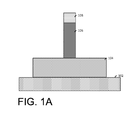
- FIG. 1A illustrates a cut-away view of a semiconductor fin arranged on a substrate.
- FIG. 1B illustrates a top view of the semiconductor fin arranged on the substrate.
- FIG. 2 illustrates a cut-away view following the deposition of a layer of spacer material over the substrate, the semiconductor fin, and the sacrificial gate.
- FIG. 3 illustrates a cut-away view following an anisotropic etching process that removes exposed portions of the layer of spacer material.
- FIGS. 4-6 illustrate another example of forming spacers along sidewalls of a sacrificial gate where the pitch of the sacrificial gates is high.
- FIG. 4 illustrates a cut-away view of the sacrificial gates that are arranged on the semiconductor fin.
- FIG. 5 illustrates a cut-away view following the deposition of a layer of spacer material over the substrate, the semiconductor fin, the sacrificial gate and the hardmask.
- FIG. 6 illustrates a cut-away view following an anisotropic etching process that removes portions of the layer of spacer material.
- FIGS. 7-19B Illustrate an exemplary method for forming a finFET device with sidewall spacers.
- FIG. 7 illustrates a side view of a semiconductor-on-insulator (SOI) wafer.
- SOI semiconductor-on-insulator
- FIG. 8A illustrates a cut-away view along the line A-A (of FIG. 8B ) following the formation of fins on the insulator layer.
- FIG. 8B illustrates a top view of the fin 804 arranged on the insulator layer.
- FIG. 9 illustrates a cut-away view following the deposition of an oxide layer over the insulator layer and the fin.
- FIG. 10 illustrates a cut-away view following the deposition of a layer of sacrificial gate material.
- FIG. 11A illustrates a cut-away view along the line B-B (of FIG. 11B ) following a lithographic patterning and etching process.
- FIG. 11B illustrates a top view following the formation of the sacrificial gates.
- FIG. 12 illustrates a cut-away view following the formation of a hydrogen (H) terminated surface on the exposed sidewalls of the sacrificial gates
- FIG. 13 illustrates a cut-away view following the formation of spacers on the hydrogen-terminated surfaces.
- FIG. 14 illustrates a top view following the removal of exposed portions of the oxide layer (of FIG. 13 ).
- FIG. 15 illustrates a top view following the formation of source/drain regions.
- FIG. 16A illustrates a top view following the deposition of an inter-level dielectric layer over the source/drain regions and portions of the insulating layer.
- FIG. 16B illustrates a cut-away view along the line A-A (of FIG. 16A ) showing the fin, the source/drain region, and the inter-level dielectric layer.
- FIG. 17 illustrates a top view following a planarization process.
- FIG. 18 illustrates a top view of the resultant structure following the removal of the sacrificial gates (of FIG. 17 ) to form cavities that expose the channel regions of the fins.
- FIG. 19A illustrates a top view of the resultant structure following the formation of a replacement metal gate stack (gate stack).
- FIG. 19B illustrates a cut-away view of the gate stack along the line C-C (of FIG. 19A ).
- a sacrificial gate is formed over a channel region of a semiconductor fin.
- Spacers are formed along sidewalls of the sacrificial gate.
- the spacers are often formed by depositing a layer of spacer material over the sacrificial gate. An anisotropic etching process is performed to remove portions of the layer of spacer material generally arranged orthogonally with respect to the sacrificial gate.
- FIGS. 1A-3 illustrate an example of forming spacers along the sidewalls of a sacrificial gate.
- FIG. 1A illustrates a cut-away view of a semiconductor fin 104 arranged on a substrate 102 .
- a sacrificial gate 106 and hardmask 108 are arranged over a channel region of the semiconductor fin 104 .
- the sacrificial gate 106 is formed by lithographically patterning and etching to remove portions of the hardmask 108 and underlying portions of the semiconductor fin material.
- the sidewalls of the sacrificial gate 106 are generally flush with the edges of the sacrificial gate 106 .
- FIG. 1B illustrates a top view of the semiconductor fin 104 arranged on the substrate 102 .
- FIG. 2 illustrates a cut-away view following the deposition of a layer of spacer material 202 over the substrate 102 , the semiconductor fin 104 , and the sacrificial gate 106 .
- FIG. 3 illustrates a cut-away view following an anisotropic etching process that removes exposed portions of the layer of spacer material 202 (of FIG. 2 ) to form spacers 302 along sidewalls of the sacrificial gate 106 .
- FIGS. 4-6 illustrate another example of forming spacers along sidewalls of a sacrificial gate where the sacrificial gate is tall.
- the sacrificial gates 106 are arranged on the semiconductor fin 104 and the hardmask 408 is arranged on the sacrificial gate 106 .
- the sidewalls of the sacrificial gate 106 are not flush with the edges of the hardmask 408 .
- Anisotropic etching processes generally do not etch with perfect directionality. The lateral etch (removal of sidewall material) of sacrificial gate becomes more pronounced as the gate height increases.
- FIG. 5 illustrates a cut-away view following the deposition of a layer of spacer material 202 over the substrate 102 , the semiconductor fin 104 , the sacrificial gate 106 and the hardmask 408 .
- FIG. 6 illustrates a cut-away view following an anisotropic etching process that removes portions of the layer of spacer material.
- portions 602 of the layer of spacer material remain un-etched between the sacrificial gates 106 due to the greater widths of the hardmasks 408 compared to widths of the sacrificial gate 106 .
- the etching process does not sufficiently remove portions of the layer of spacer material to form the desired spacer arrangement.
- the portions 602 remain on the semiconductor fin 104 , and are undesirable since they obscure active regions of the semiconductor fin 602 . This may reduce the performance of the resultant finFET devices.
- FIGS. 7-19B Illustrate an exemplary method for forming a finFET device with sidewall spacers.
- FIG. 7 illustrates a side view of a semiconductor-on-insulator (SOI) wafer 701 .
- the SOI wafer 701 includes a substrate 703 , an insulator layer 702 arranged on the substrate, and a semiconductor channel layer 704 arranged on the insulator layer 702 .
- the SOI wafer 701 can be formed by any suitable technique such as, for example wafer bonding, SmartcutTM, SIMOX (Separation by IMplanted Oxygen). Though the illustrated exemplary embodiment includes a semiconductor-on-insulator wafer 701 alternate exemplary embodiments may be formed using, for example, a bulk semiconductor substrate.
- the semiconductor channel layer may also comprise an organic semiconductor or a layered semiconductor such as, for example, Si/SiGe, a silicon-on-insulator or a SiGe-on-insulator. A portion or entire semiconductor channel layer may be amorphous, polycrystalline, or monocrystalline.
- the semiconductor channel layer employed in the present invention may also comprise a hybrid oriented (HOT) semiconductor channel layer in which the HOT substrate has surface regions of different crystallographic orientation.
- the semiconductor channel layer may be doped, undoped or contain doped regions and undoped regions therein.
- the semiconductor channel layer may contain regions with strain and regions without strain therein, or contain regions of tensile strain and compressive strain.
- the insulator layer 702 may include, for example, a buried oxide (BOX) material or other suitable insulator materials.
- suitable insulator materials include, silicon oxide, silicon nitride, silicon oxynitride, boron nitride, high-k materials, or any combination of these materials.
- high-k materials include but are not limited to metal oxides such as hafnium oxide, hafnium silicon oxide, hafnium silicon oxynitride, lanthanum oxide, lanthanum aluminum oxide, zirconium oxide, zirconium silicon oxide, zirconium silicon oxynitride, tantalum oxide, titanium oxide, barium strontium titanium oxide, barium titanium oxide, strontium titanium oxide, yttrium oxide, aluminum oxide, lead scandium tantalum oxide, and lead zinc niobate.
- the high-k may further include dopants such as lanthanum, aluminum.
- the thickness of insulator layer 702 generally varies and is not intended to be limited. In one aspect, the thickness of the insulator layer 702 is in a range from about 10 nm to about 1000 nm.
- the insulator layer 702 can be formed by any suitable process such as thermal oxidation, thermal nitridation, chemical vapor deposition (CVD).
- a hardmask layer 708 is arranged on the semiconductor channel layer 704 .
- the hardmask layer 708 may include, for example, silicon oxide, silicon nitride (SiN), SiOCN, SiBCN or any suitable combination of those.
- the hardmask layer 708 may be deposited using a deposition process, including, but not limited to, PVD, CVD, PECVD, or any combination thereof.
- FIG. 8A illustrates a cut-away view along the line A-A (of FIG. 8B ) following the formation of fins 804 on the insulator layer 702 .
- the fins 804 may be patterned by, for example, a lithographic patterning and etching process such as, reactive ion etching (ME) or a sidewall imaging transfer process that removes exposed portions of the hardmask layer 708 and portions of the semiconductor channel layer 704 to expose portions of the insulator layer 702 .
- FIG. 8B illustrates a top view of the fin 804 arranged on the insulator layer 702 .
- the substrate 703 (of FIG. 7 has been omitted from the subsequent figures.)
- FIG. 9 illustrates a cut-away view following the deposition of an oxide layer 902 over the insulator layer 702 and the fin 804 .
- the hardmask layer 708 (of FIG. 8A ) has been removed prior to depositing the oxide layer 902 .
- oxides include silicon dioxide, tetraethylorthosilicate (TEOS) oxide, high aspect ratio plasma (HARP) oxide, high temperature oxide (HTO), high density plasma (HDP) oxide, oxides (e.g., silicon oxides) formed by an atomic layer deposition (ALD) process, or any combination thereof.
- FIG. 10 illustrates a cut-away view following the deposition of a layer of sacrificial gate material 1002 .
- the layer of sacrificial gate material 1002 may include, for example, amorphous silicon (aSi), or polycrystalline silicon (polysilicon) material or another suitable sacrificial gate material.
- the layer sacrificial gate material 1002 may be deposited by a deposition process, including, but not limited to, physical vapor deposition (PVD), chemical vapor deposition (CVD), atomic layer deposition (ALD, plasma enhanced chemical vapor deposition (PECVD), inductively coupled plasma chemical vapor deposition (ICP CVD), or any combination thereof.
- PVD physical vapor deposition
- CVD chemical vapor deposition
- ALD atomic layer deposition
- PECVD plasma enhanced chemical vapor deposition
- ICP CVD inductively coupled plasma chemical vapor deposition
- a hard mask layer 1004 such as, for example, silicon oxide, silicon nitride (SiN), SiOCN, SiBCN or any suitable combination of those materials, is deposited on the layer of sacrificial gate material 1002 .
- the hardmask layer 1004 may be deposited using a deposition process, including, but not limited to, PVD, CVD, PECVD, or any combination thereof.
- FIG. 11A illustrates a cut-away view along the line B-B (of FIG. 11B ) following a lithographic patterning and etching process such as, for example, reactive ion etching or a wet etching process that is performed to remove exposed portions of the hardmask layer 1004 (of FIG. 10 ) and the layer of sacrificial gate material 1002 form the sacrificial gates 1102 and the sacrificial gate caps 1104 .
- the sacrificial gates 1102 have a width W 2 and the sacrificial gate caps 1104 have a width W 1 , where W 1 >W 2 .
- FIG. 11B illustrates a top view following the formation of the sacrificial gates 1102 .
- FIG. 12 illustrates a cut-away view following the formation of a hydrogen (H) terminated surface 1202 on the exposed sidewalls of the sacrificial gates 1102 .
- the hydrogen-terminated surfaces 1202 are formed by performing an annealing process in H 2 ambience.
- the H-terminated surface will only be formed on Si surface because dangling bonds are present on the exposed Si surface.
- the process results in the hydrogen-terminated surfaces 1202 on exposed portions of the sacrificial gates 1102 .
- FIG. 13 illustrates a cut-away view following the formation of spacers 1302 on the hydrogen-terminated surfaces 1202 .
- the spacers 1302 are formed using, for example, an atomic layer deposition (ALD) process that selectively deposits a nitride material such as, for example, silicon nitride on exposed hydrogen-terminated surfaces 1202 .
- ALD atomic layer deposition
- FIG. 14 illustrates a top view following the removal of exposed portions of the oxide layer 902 (of FIG. 13 ).
- FIG. 15 illustrates a top view following the formation of source/drain regions 1502 .
- the source/drain regions 1502 are formed by an epitaxial growth process that deposits a crystalline overlayer of semiconductor material onto the exposed crystalline seed material of the exposed fin 804 to form the source/drain regions 1502 .
- Epitaxial materials may be grown from gaseous or liquid precursors. Epitaxial materials may be grown using vapor-phase epitaxy (VPE), molecular-beam epitaxy (MBE), liquid-phase epitaxy (LPE), or other suitable process.
- VPE vapor-phase epitaxy
- MBE molecular-beam epitaxy
- LPE liquid-phase epitaxy
- Epitaxial silicon, silicon germanium, and/or carbon doped silicon (Si:C) silicon can be doped during deposition (in-situ doped) by adding dopants, n-type dopants (e.g., phosphorus or arsenic) or p-type dopants (e.g., boron or gallium), depending on the type of transistor.
- the dopant concentration in the source/drain can range from 1 ⁇ 10 19 cm ⁇ 3 to 2 ⁇ 10 21 cm ⁇ 3 , or preferably between 2 ⁇ 10 20 cm ⁇ 3 to 1 ⁇ 10 21 cm ⁇ 3 .
- epitaxial growth and/or deposition and “epitaxially formed and/or grown” mean the growth of a semiconductor material (crystalline material) on a deposition surface of another semiconductor material (crystalline material), in which the semiconductor material being grown (crystalline overlayer) has substantially the same crystalline characteristics as the semiconductor material of the deposition surface (seed material).
- the chemical reactants provided by the source gases are controlled and the system parameters are set so that the depositing atoms arrive at the deposition surface of the semiconductor channel layer with sufficient energy to move about on the surface such that the depositing atoms orient themselves to the crystal arrangement of the atoms of the deposition surface.
- an epitaxially grown semiconductor material has substantially the same crystalline characteristics as the deposition surface on which the epitaxially grown material is formed.
- an epitaxially grown semiconductor material deposited on a ⁇ 100 ⁇ orientated crystalline surface will take on a ⁇ 100 ⁇ orientation.
- epitaxial growth and/or deposition processes are selective to forming on semiconductor surface, and generally do not deposit material on exposed surfaces, such as silicon dioxide or silicon nitride surfaces.
- the gas source for the deposition of epitaxial semiconductor material include a silicon containing gas source, a germanium containing gas source, or a combination thereof.
- a silicon gas source that is selected from the group consisting of silane, disilane, trisilane, tetrasilane, hexachlorodisilane, tetrachlorosilane, dichlorosilane, trichlorosilane, methylsilane, dimethylsilane, ethylsilane, methyldisilane, dimethyldisilane, hexamethyldisilane and combinations thereof.
- An epitaxial germanium layer can be deposited from a germanium gas source that is selected from the group consisting of germane, digermane, halogermane, dichlorogermane, trichlorogermane, tetrachlorogermane and combinations thereof. While an epitaxial silicon germanium alloy layer can be formed utilizing a combination of such gas sources. Carrier gases like hydrogen, nitrogen, helium and argon may be used.
- FIG. 16A illustrates a top view following the deposition of an inter-level dielectric layer 1602 over the source/drain regions 1502 and portions of the insulating layer 702 .
- the inter-level dielectric layer 1602 is formed from, for example, a low-k dielectric material (with k ⁇ 4.0), including but not limited to, silicon oxide, spin-on-glass, a flowable oxide, a high density plasma oxide, borophosphosilicate glass (BPSG), or any combination thereof.
- the inter-level dielectric layer 1602 is deposited by a deposition process, including, but not limited to CVD, PVD, plasma enhanced CVD, atomic layer deposition (ALD), evaporation, chemical solution deposition, or like processes.
- FIG. 16B illustrates a cut-away view along the line A-A (of FIG. 16A ) showing the fin 802 , the source/drain region 1502 , and the inter-level dielectric layer 1602 .
- FIG. 17 illustrates a top view following a planarization process such as, for example, chemical mechanical polishing.
- the planarization process removes portions of the inter-level dielectric layer 1602 and the hardmask layer 1104 (of FIG. 16A ) to expose the sacrificial gates 1102 and the spacers 1302 .
- FIG. 18 illustrates a top view of the resultant structure following the removal of the sacrificial gates 1102 (of FIG. 17 ) to form cavities 1802 that expose the channel regions of the fins 802 .
- the sacrificial gates 1102 may be removed by performing a dry etch process, for example, RIE, followed by a wet etch process.
- the wet etch process is selective to (will not substantially etch) the spacers 1302 and the inter-level dielectric material.
- the chemical etch process may include, but is not limited to, hot ammonia or tetramethylammonium hydroxide (TMAH).
- FIG. 19A illustrates a top view of the resultant structure following the formation of a replacement metal gate stack (gate stack) 1901 .
- FIG. 19B illustrates a cut-away view of the gate stack 1901 along the line C-C (of FIG. 19A ).
- the gate stack 1901 include high-k metal gates formed, for example, by filling the cavity 1802 (of FIG. 18 ) with one or more gate dielectric 1902 materials, one or more workfunction metals 1904 , and one or more metal gate conductor 1906 materials.
- the gate dielectric 1902 material(s) can be a dielectric material having a dielectric constant greater than 3.9, 7.0, or 10.0.
- Non-limiting examples of suitable materials for the dielectric 1902 materials include oxides, nitrides, oxynitrides, silicates (e.g., metal silicates), aluminates, titanates, nitrides, or any combination thereof.
- high-k materials include, but are not limited to, metal oxides such as hafnium oxide, hafnium silicon oxide, hafnium silicon oxynitride, lanthanum oxide, lanthanum aluminum oxide, zirconium oxide, zirconium silicon oxide, zirconium silicon oxynitride, tantalum oxide, titanium oxide, barium strontium titanium oxide, barium titanium oxide, strontium titanium oxide, yttrium oxide, aluminum oxide, lead scandium tantalum oxide, and lead zinc niobate.
- the high-k material may further include dopants such as, for example, lanthanum and aluminum.
- the gate dielectric 1902 materials may be formed by suitable deposition processes, for example, chemical vapor deposition (CVD), plasma-enhanced chemical vapor deposition (PECVD), atomic layer deposition (ALD), evaporation, physical vapor deposition (PVD), chemical solution deposition, or other like processes.
- CVD chemical vapor deposition
- PECVD plasma-enhanced chemical vapor deposition
- ALD atomic layer deposition
- evaporation evaporation
- PVD physical vapor deposition
- chemical solution deposition evapor deposition
- the thickness of the dielectric material may vary depending on the deposition process as well as the composition and number of high-k dielectric materials used.
- the dielectric material layer may have a thickness in a range from about 0.5 to about 20 nm.
- the work function metal(s) 1904 may be disposed over the gate dielectric 1902 material.
- the type of work function metal(s) 1904 depends on the type of transistor and may differ between the nFET and pFET devices.
- suitable work function metals 1904 include p-type work function metal materials and n-type work function metal materials.
- P-type work function materials include compositions such as ruthenium, palladium, platinum, cobalt, nickel, and conductive metal oxides, or any combination thereof.
- N-type metal materials include compositions such as hafnium, zirconium, titanium, tantalum, aluminum, metal carbides (e.g., hafnium carbide, zirconium carbide, titanium carbide, and aluminum carbide), aluminides, or any combination thereof.
- the work function metal(s) may be deposited by a suitable deposition process, for example, CVD, PECVD, PVD, plating, thermal or e-beam evaporation, and sputtering.
- the gate conductor 1906 material(s) is deposited over the gate dielectric 1902 materials and work function metal(s) 1904 to form the gate stack 1901 .
- suitable conductive metals include aluminum (Al), platinum (Pt), gold (Au), tungsten (W), titanium (Ti), or any combination thereof.
- the gate conductor 1906 material(s) may be deposited by a suitable deposition process, for example, CVD, PECVD, PVD, plating, thermal or e-beam evaporation, and sputtering.
- planarization process for example, chemical mechanical planarization (CMP) is performed to remove the overburden of the deposited gate materials and form the gate stack 1901 .
- CMP chemical mechanical planarization
- additional insulating material may be deposited over the device(s).
- the insulating material may be patterned to form cavities (not shown) that expose portions of the source/drain region 1502 and the gate stack 1901 .
- the cavities may be filled by a conductive material (not shown) and, in some embodiments, a liner layer (not shown) to form conductive contacts (not shown).
- the methods and resultant structures described herein provide for forming gate stacks of finFET devices with a tight pitch.
- the methods use a process to form a hydrogen annealed surface on the sidewalls of the sacrificial gate stacks.
- the hydrogen annealed surface provides a surface for selectively depositing spacer material on the sidewalls of the sacrificial gates.
- the spacer material is thus formed as desired along the sidewalls of the sacrificial gates, and is not substantially deposited on the fin surfaces.
- the methods and resultant structures provide for forming spacers without undesirable spacer material being arranged on active surfaces of the device.
- invention or “present invention” are non-limiting terms and not intended to refer to any single aspect of the particular invention but encompass all possible aspects as described in the specification and the claims.
- the term “on” may refer to an element that is on, above or in contact with another element or feature described in the specification and/or illustrated in the figures.
- the term “about” modifying the quantity of an ingredient, component, or reactant of the invention employed refers to variation in the numerical quantity that can occur, for example, through typical measuring and liquid handling procedures used for making concentrates or solutions. Furthermore, variation can occur from inadvertent error in measuring procedures, differences in the manufacture, source, or purity of the ingredients employed to make the compositions or carry out the methods, and the like.
- the term “about” means within 10% of the reported numerical value.
- the term “about” means within 5% of the reported numerical value.
- the term “about” means within 10, 9, 8, 7, 6, 5, 4, 3, 2, or 1% of the reported numerical value.
Landscapes
- Engineering & Computer Science (AREA)
- Microelectronics & Electronic Packaging (AREA)
- Power Engineering (AREA)
- Condensed Matter Physics & Semiconductors (AREA)
- General Physics & Mathematics (AREA)
- Physics & Mathematics (AREA)
- Computer Hardware Design (AREA)
- Manufacturing & Machinery (AREA)
- Ceramic Engineering (AREA)
- Chemical & Material Sciences (AREA)
- Chemical Kinetics & Catalysis (AREA)
- Composite Materials (AREA)
- Materials Engineering (AREA)
- Thin Film Transistor (AREA)
- Insulated Gate Type Field-Effect Transistor (AREA)
Abstract
Description
Claims (19)
Priority Applications (2)
Application Number | Priority Date | Filing Date | Title |
---|---|---|---|
US15/181,946 US9876097B2 (en) | 2016-06-14 | 2016-06-14 | Selectively formed gate sidewall spacer |
US15/818,828 US10833176B2 (en) | 2016-06-14 | 2017-11-21 | Selectively formed gate sidewall spacer |
Applications Claiming Priority (1)
Application Number | Priority Date | Filing Date | Title |
---|---|---|---|
US15/181,946 US9876097B2 (en) | 2016-06-14 | 2016-06-14 | Selectively formed gate sidewall spacer |
Related Child Applications (1)
Application Number | Title | Priority Date | Filing Date |
---|---|---|---|
US15/818,828 Division US10833176B2 (en) | 2016-06-14 | 2017-11-21 | Selectively formed gate sidewall spacer |
Publications (2)
Publication Number | Publication Date |
---|---|
US20170358664A1 US20170358664A1 (en) | 2017-12-14 |
US9876097B2 true US9876097B2 (en) | 2018-01-23 |
Family
ID=60573162
Family Applications (2)
Application Number | Title | Priority Date | Filing Date |
---|---|---|---|
US15/181,946 Expired - Fee Related US9876097B2 (en) | 2016-06-14 | 2016-06-14 | Selectively formed gate sidewall spacer |
US15/818,828 Active 2036-09-27 US10833176B2 (en) | 2016-06-14 | 2017-11-21 | Selectively formed gate sidewall spacer |
Family Applications After (1)
Application Number | Title | Priority Date | Filing Date |
---|---|---|---|
US15/818,828 Active 2036-09-27 US10833176B2 (en) | 2016-06-14 | 2017-11-21 | Selectively formed gate sidewall spacer |
Country Status (1)
Country | Link |
---|---|
US (2) | US9876097B2 (en) |
Families Citing this family (3)
Publication number | Priority date | Publication date | Assignee | Title |
---|---|---|---|---|
US10141231B1 (en) * | 2017-08-28 | 2018-11-27 | Taiwan Semiconductor Manufacturing Co., Ltd. | FinFET device with wrapped-around epitaxial structure and manufacturing method thereof |
US10106892B1 (en) * | 2017-08-31 | 2018-10-23 | Globalfoundries Inc. | Thermal oxide equivalent low temperature ALD oxide for dual purpose gate oxide and method for producing the same |
CN113327979B (en) * | 2020-02-28 | 2023-04-18 | 中芯国际集成电路制造(天津)有限公司 | Method for forming semiconductor structure |
Citations (12)
Publication number | Priority date | Publication date | Assignee | Title |
---|---|---|---|---|
US20030104707A1 (en) | 2001-11-16 | 2003-06-05 | Yoshihide Senzaki | System and method for improved thin dielectric films |
US6770516B2 (en) | 2002-09-05 | 2004-08-03 | Taiwan Semiconductor Manufacturing Company | Method of forming an N channel and P channel FINFET device on the same semiconductor substrate |
US20070020879A1 (en) | 2005-07-19 | 2007-01-25 | Samsung Electronics Co., Ltd | Method of forming an isolation layer and method of manufacturing a field effect transistor using the same |
US7172792B2 (en) | 2002-12-20 | 2007-02-06 | Applied Materials, Inc. | Method for forming a high quality low temperature silicon nitride film |
US7476578B1 (en) | 2007-07-12 | 2009-01-13 | International Business Machines Corporation | Process for finFET spacer formation |
US7579648B2 (en) | 2004-07-22 | 2009-08-25 | Samsung Electronics Co., Ltd. | Semiconductor device having a channel pattern and method of manufacturing the same |
US8174055B2 (en) | 2010-02-17 | 2012-05-08 | Globalfoundries Inc. | Formation of FinFET gate spacer |
US8637359B2 (en) * | 2011-06-10 | 2014-01-28 | International Business Machines Corporation | Fin-last replacement metal gate FinFET process |
US8716797B2 (en) | 2009-11-03 | 2014-05-06 | International Business Machines Corporation | FinFET spacer formation by oriented implantation |
US20150115371A1 (en) | 2013-10-29 | 2015-04-30 | Globalfoundries Inc. | Finfet semiconductor structures and methods of fabricating same |
US9171927B2 (en) | 2013-03-26 | 2015-10-27 | GlobalFoundries, Inc. | Spacer replacement for replacement metal gate semiconductor devices |
US9276087B2 (en) * | 2013-05-10 | 2016-03-01 | Samsung Electronics Co., Ltd. | Methods of manufacturing FINFET semiconductor devices using sacrificial gate patterns and selective oxidization of a fin |
-
2016
- 2016-06-14 US US15/181,946 patent/US9876097B2/en not_active Expired - Fee Related
-
2017
- 2017-11-21 US US15/818,828 patent/US10833176B2/en active Active
Patent Citations (12)
Publication number | Priority date | Publication date | Assignee | Title |
---|---|---|---|---|
US20030104707A1 (en) | 2001-11-16 | 2003-06-05 | Yoshihide Senzaki | System and method for improved thin dielectric films |
US6770516B2 (en) | 2002-09-05 | 2004-08-03 | Taiwan Semiconductor Manufacturing Company | Method of forming an N channel and P channel FINFET device on the same semiconductor substrate |
US7172792B2 (en) | 2002-12-20 | 2007-02-06 | Applied Materials, Inc. | Method for forming a high quality low temperature silicon nitride film |
US7579648B2 (en) | 2004-07-22 | 2009-08-25 | Samsung Electronics Co., Ltd. | Semiconductor device having a channel pattern and method of manufacturing the same |
US20070020879A1 (en) | 2005-07-19 | 2007-01-25 | Samsung Electronics Co., Ltd | Method of forming an isolation layer and method of manufacturing a field effect transistor using the same |
US7476578B1 (en) | 2007-07-12 | 2009-01-13 | International Business Machines Corporation | Process for finFET spacer formation |
US8716797B2 (en) | 2009-11-03 | 2014-05-06 | International Business Machines Corporation | FinFET spacer formation by oriented implantation |
US8174055B2 (en) | 2010-02-17 | 2012-05-08 | Globalfoundries Inc. | Formation of FinFET gate spacer |
US8637359B2 (en) * | 2011-06-10 | 2014-01-28 | International Business Machines Corporation | Fin-last replacement metal gate FinFET process |
US9171927B2 (en) | 2013-03-26 | 2015-10-27 | GlobalFoundries, Inc. | Spacer replacement for replacement metal gate semiconductor devices |
US9276087B2 (en) * | 2013-05-10 | 2016-03-01 | Samsung Electronics Co., Ltd. | Methods of manufacturing FINFET semiconductor devices using sacrificial gate patterns and selective oxidization of a fin |
US20150115371A1 (en) | 2013-10-29 | 2015-04-30 | Globalfoundries Inc. | Finfet semiconductor structures and methods of fabricating same |
Non-Patent Citations (2)
Title |
---|
Dumas, P. et al., "Morphology of hydrogen-terminated Si (111) and Si (100) surfaces upon etching in HF and buffered-HF solutions," Surface Science, vol. 269/270, 1992, pp. 867-878. |
Yokoyama, S. et al., "Atomic-layer selective deposition of silicon nitride on hydrogen-terminated Si surfaces," Applied Surface Science, vol. 130-132, 1998, pp. 352-356. |
Also Published As
Publication number | Publication date |
---|---|
US10833176B2 (en) | 2020-11-10 |
US20180076305A1 (en) | 2018-03-15 |
US20170358664A1 (en) | 2017-12-14 |
Similar Documents
Publication | Publication Date | Title |
---|---|---|
US10396181B2 (en) | Forming stacked nanowire semiconductor device | |
US10062615B2 (en) | Stacked nanowire devices | |
US10332883B2 (en) | Integrated metal gate CMOS devices | |
US10256161B2 (en) | Dual work function CMOS devices | |
US9882028B2 (en) | Pitch split patterning for semiconductor devices | |
US9917089B2 (en) | III-V semiconductor CMOS FinFET device | |
US9704859B1 (en) | Forming semiconductor fins with self-aligned patterning | |
US10608080B2 (en) | Bulk to silicon on insulator device | |
US10833176B2 (en) | Selectively formed gate sidewall spacer | |
US9698266B1 (en) | Semiconductor device strain relaxation buffer layer | |
US9859389B1 (en) | Sidewall protective layer for contact formation | |
US9859174B1 (en) | Sidewall image transfer structures | |
US10242983B2 (en) | Semiconductor device with increased source/drain area | |
US10157827B2 (en) | Semiconductor contact |
Legal Events
Date | Code | Title | Description |
---|---|---|---|
AS | Assignment |
Owner name: INTERNATIONAL BUSINESS MACHINES CORPORATION, NEW Y Free format text: ASSIGNMENT OF ASSIGNORS INTEREST;ASSIGNORS:CHENG, KANGGUO;MIAO, XIN;XU, WENYU;AND OTHERS;REEL/FRAME:038910/0641 Effective date: 20160614 |
|
STCF | Information on status: patent grant |
Free format text: PATENTED CASE |
|
FEPP | Fee payment procedure |
Free format text: MAINTENANCE FEE REMINDER MAILED (ORIGINAL EVENT CODE: REM.); ENTITY STATUS OF PATENT OWNER: LARGE ENTITY |
|
LAPS | Lapse for failure to pay maintenance fees |
Free format text: PATENT EXPIRED FOR FAILURE TO PAY MAINTENANCE FEES (ORIGINAL EVENT CODE: EXP.); ENTITY STATUS OF PATENT OWNER: LARGE ENTITY |
|
STCH | Information on status: patent discontinuation |
Free format text: PATENT EXPIRED DUE TO NONPAYMENT OF MAINTENANCE FEES UNDER 37 CFR 1.362 |
|
FP | Lapsed due to failure to pay maintenance fee |
Effective date: 20220123 |