US9871516B2 - Transmitting apparatus with source termination - Google Patents
Transmitting apparatus with source termination Download PDFInfo
- Publication number
- US9871516B2 US9871516B2 US14/296,377 US201414296377A US9871516B2 US 9871516 B2 US9871516 B2 US 9871516B2 US 201414296377 A US201414296377 A US 201414296377A US 9871516 B2 US9871516 B2 US 9871516B2
- Authority
- US
- United States
- Prior art keywords
- inductive element
- driver
- driver output
- differential
- mode signal
- Prior art date
- Legal status (The legal status is an assumption and is not a legal conclusion. Google has not performed a legal analysis and makes no representation as to the accuracy of the status listed.)
- Active
Links
Images


Classifications
-
- H—ELECTRICITY
- H03—ELECTRONIC CIRCUITRY
- H03K—PULSE TECHNIQUE
- H03K19/00—Logic circuits, i.e. having at least two inputs acting on one output; Inverting circuits
- H03K19/0005—Modifications of input or output impedance
-
- H—ELECTRICITY
- H03—ELECTRONIC CIRCUITRY
- H03K—PULSE TECHNIQUE
- H03K19/00—Logic circuits, i.e. having at least two inputs acting on one output; Inverting circuits
- H03K19/003—Modifications for increasing the reliability for protection
- H03K19/00346—Modifications for eliminating interference or parasitic voltages or currents
Definitions
- This disclosure pertains in general to data communications, and more specifically to signal integrity on a chip to chip communication.
- Video and audio data are typically transferred from one device to another across using communication links.
- an advanced protocol such as the high definition multimedia interface (HDMI) or the mobile high definition link (MHL)
- one device may communicate with another using a common mode signal superimposed on a differential mode signal.
- the common mode signal may generate Electromagnetic Interference (EMI).
- EMI Electromagnetic Interference
- a common mode choke may be employed between the two devices. However, the common mode choke may degrade the signal quality from the transmitting device.
- Embodiments of the present disclosure relate to a transmitting apparatus with an improved source termination for a chip to chip communication in a manner that properly terminates an output of the transmitter, maintains the signal quality, and reduces EMI.
- an apparatus for transmitting a signal with an improved termination includes a driver to generate a differential mode signal superimposed on a common mode signal at a differential driver output of the driver.
- the differential driver output includes a first driver output and a second driver output.
- the apparatus also includes a termination circuit coupled between the first driver output and the second driver output.
- the termination circuit includes a capacitor connected to a node.
- the termination circuit also includes a first resistor and a first inductive element coupled in series between the first driver output and the node.
- the termination circuit includes a second resistor and a second inductive element coupled in series between the second driver output and the node. The first inductive element and second inductive element causes peaking in the differential mode signal at the differential driver output.
- the apparatus further includes a first switch coupled in series with the first resistor and the first inductive element between the first driver output and the node.
- the apparatus also includes a second switch coupled in series with the second resistor and the second inductive element between the second driver output and the node.
- the first switch and second switch are closed when the apparatus is communicating through a first communication protocol.
- the first switch and the second switch are open when the apparatus is communicating through a second communication protocol.
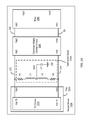
- FIG. 1 is a high-level block diagram of a system for multimedia data communications, according to one embodiment.
- FIG. 2A is a block diagram of a source device, according to one embodiment.
- FIG. 2B is an impedance plot of a termination circuit for a common mode signal versus frequency.
- FIG. 2C is an impedance plot of a termination circuit for a differential mode signal versus frequency, according to one embodiment.
- FIG. 2D is an insertion loss plot of a termination circuit for a differential mode signal versus frequency, according to one embodiment.
- FIG. 3 is an illustration of a signal transmitted from the source device including a differential mode signal and a common mode signal, according to one embodiment.
- FIGS. 4A and 4B are illustrations of common mode and differential mode signals with various termination configurations at an output of a driver and an output of a port, according to one embodiment.
- FIG. 5 is an illustration of a block diagram of a source device with a transmitter integrated circuit (IC) including switches for enabling the termination, according to one embodiment.
- IC transmitter integrated circuit
- FIG. 6 is an illustration of a block diagram of a source device with a transmitter IC including switches and resistors, according to one embodiment.
- FIG. 7 is an illustration of a block diagram of a source device with a transmitter IC including switches, resistors and inductors, according to one embodiment.
- FIG. 8 is an illustration of a block diagram of a source device with a transmitter IC including switches, resistors, inductors, and a capacitor, according to one embodiment.
- FIG. 9 is an illustration of a block diagram of a source device with a transmitter IC including switches, resistors, and bonding inductors, according to one embodiment.
- directly connected means that two components are directly connected to each other without any intervening components.
- coupled means that two components may be directly connected to each other or that intervening components may be located between two components.
- Embodiments of the present disclosure include a transmitter with a termination circuit that does not degrade signal quality.
- the transmitter communicates with a receiver through a differential signal including a differential mode signal and a common mode signal.
- the termination circuit ensures signal integrity of signals produced from the transmitter in a chip to chip communication.
- the termination circuit enables a proper termination to reduce unwanted interference from one device to another.
- FIG. 1 is a high-level block diagram of a system 100 for data communications, according to one embodiment.
- the system 100 includes a source device 110 communicating with a sink device 115 through one or more communication media (e.g., one or more interface cables 120 , 150 , 180 ).
- Source device 110 transmits multimedia data streams (e.g., audio/video streams) to the sink device 115 and also exchanges control data with the sink device 115 through the interface cables 120 , 150 , 180 .
- source device 110 and/or sink device 115 may be repeater devices.
- Source device 110 includes physical communication ports 112 , 142 , 172 for coupling to the interface cables 120 , 150 , 180 .
- Sink device 115 also includes physical communication ports 117 , 147 , 177 for coupling to the interface cables 120 , 150 , 180 . Signals exchanged between the source device 110 and the sink device 115 across the interface cables 120 , 150 , 180 pass through the physical communication ports.
- interface cable 150 represents a Mobile High-Definition Link (MHL) cable.
- MHL Mobile High-Definition Link
- the MHL cable 150 supports differential signals transmitted via data 0 + line 151 , data 0 ⁇ line 152 , data 1 + line 153 , data 1 ⁇ line 154 , data 2 + line 155 and data 2 ⁇ line 156 .
- there may only be a single pair of differential data lines e.g., 151 and 152 ).
- Embedded common mode clocks are transmitted through the differential data lines.
- the MHL cable 150 may further include a control bus (CBUS) 159 , power 160 and ground 161 .
- the CBUS 159 carries control information such as discovery data, configuration data and remote control commands.
- interface cable 120 represents a High Definition Multimedia Interface (HDMI) cable.
- HDMI cable 120 supports differential signals transmitted via data 0 + line 121 , data 0 ⁇ line 122 , data 1 + line 123 , data 1 ⁇ line 124 , data 2 + line 125 , and data 2 ⁇ line 126 .
- the HDMI cable 120 may further include differential clock lines clock+ 127 and clock ⁇ 128 ; Consumer Electronics Control (CEC) control bus 129 ; Display Data Channel (DDC) bus 130 ; power 131 , ground 132 ; hot plug detect 133 ; and four shield lines 134 for the differential signals.
- the sink device 115 may utilize the CEC control bus 129 for the transmission of closed loop feedback control data to source device 110 .
- a representation of the source device 110 , the sink device 115 , or components within the source device 110 or sink device 115 may be stored as data in a non-transitory computer-readable medium (e.g. hard disk drive, flash drive, optical drive).
- a non-transitory computer-readable medium e.g. hard disk drive, flash drive, optical drive.
- These representations may be behavioral level, register transfer level, logic component level, transistor level and layout geometry-level descriptions.
- FIG. 2A is a block diagram of a source device 110 A, according to one embodiment.
- the source device 110 A includes a transmitter integrated circuit (TXIC) 230 A, a termination circuit 215 A, a common mode choke circuit 220 and a port 250 .
- a positive output pin Vop 1 of the TXIC 230 A is coupled to a positive input pin Vip 2 of the common mode choke circuit 220 via a connection 212 .
- a negative output pin Von 1 of the TXIC 230 A is coupled to the negative input pin Vin 2 of the common mode choke circuit 220 via a connection 214 .
- the termination circuit 215 A is coupled between the positive output pin Vop 1 and the negative output pin Von 1 of the TXIC 230 A.
- a positive output pin Vop 2 of the common mode choke circuit 220 is coupled to a positive input pin Vip 3 of the port 250 via a connection 222 .
- a negative output pin Von 2 of the common mode choke circuit 220 is coupled to a negative input pin Vin 3 of the port 250 via a connection 224 .
- the TXIC 230 A includes a transmitter driver (TX driver) 210 that drives a differential signal onto the driver outputs Vop and Von that includes a differential mode signal and a common mode signal.
- the differential mode signal typically operates at a higher frequency than the common mode signal.
- the differential mode signal operates at 3 GHz and represents data for a multimedia stream.
- the common mode signal is a clock that operates at 75 MHz.
- the differential mode signal can represent one data stream (e.g. Ethernet data) while the common mode signal represents another data stream (e.g. audio data).
- the TX driver 210 includes a differential driver to generate the differential mode signal and a common mode driver to generate the common mode signal.
- a positive output pin Vop TX of the TX driver 210 is coupled to the positive output pin Vop 1 of the TXIC 230 A to transmit a positive signal of the differential signal.
- a negative output pin Von TX of the TX driver 210 is coupled to the negative output pin Von 1 of the TXIC 230 A to transmit a negative signal of the differential signal.
- the common mode choke circuit 220 is coupled between the differential outputs Vop 1 and Von 1 of the TX driver 210 .
- the common mode choke circuit 220 suppresses common mode noise generated from the TXIC 230 A.
- the common mode choke circuit 220 is formed with a transformer.
- the transformer may be configured such that magnetic fluxes generated from the common mode signal by the TX driver 210 are added together.
- the common mode choke circuit 220 acts as an inductor to suppress the common mode noise at a high frequency and passes the common mode signal at a low frequency.
- the transformer is also configured such that magnetic fluxes generated from the differential signal by the TX driver 210 are cancelled with each other.
- the common mode choke circuit 220 passes the differential mode signal without substantial loss.
- the port 250 provides a physical interface to mate with an interface cable 120 as described herein with respect to FIG. 1 .
- the port 250 may be the port 112 of FIG. 1 .
- the port 250 may be the port 142 of FIG. 1 .
- an electrostatic discharge (ESD) protection circuit may be implemented between the common mode choke circuit 220 and the port 250 to alleviate a sudden flow of electricity between the TXIC 230 A and the port 250 .
- the termination circuit 215 A enables a proper termination to guarantee adequate signal quality and reduce the EMI from the TXIC 230 A.
- the termination circuit 215 A includes passive components such as a first resistor R 1 , a second resistor R 2 , a first inductor L 1 , a second inductor L 2 and a capacitor C 1 .
- the passive components are implemented external to the TXIC 230 A on a printed circuit board (PCB).
- the first resistor R 1 and the first inductor L 1 are coupled in series between the positive output pin Vop 1 of the TXIC 230 A and a common node Ncm.
- one end of the first resistor R 1 is coupled to the positive output pin Vop 1
- another end of the first resistor R 1 is coupled to one end of the first inductor L 1 .
- another end of the first inductor L 1 is coupled to the common node Ncm.
- the first resistor R 1 and the inductor L 1 may be swapped.
- the second resistor R 2 and the second inductor L 2 are coupled in series between the negative output Von 1 of the TXIC 230 A and the common node Ncm.
- the configuration of the second resistor R 2 , the second inductor L 2 , and the negative output pin Von 1 are substantially similar to the configuration of the first resistor R 1 , the first inductor L 1 , and the positive output pin Vop 1 . Additionally, a capacitor C 1 is coupled between the common node Ncm and ground 232 to suppress a common mode peaking in the common mode signal.
- the first resistor R 1 and the second resistor R 2 provide a termination impedance to the common mode signal.
- the capacitor C 1 removes an unwanted peaking of the common mode signal generated due to the common mode choke circuit 220 as described in details herein with respect to FIG. 4A .
- the common mode impedance 294 of the termination circuit 215 A becomes Z 2 (e.g., approximately 50 Ohm) at the common mode operating frequency fcm, because both the inductive elements L 1 and L 2 become substantially shorted.
- the common mode impedance 294 increases as the frequency increases, because the impedance of each of the inductive elements L 1 and L 2 increases.
- values for the inductive elements L 1 and L 2 can be chosen such that at three times the frequency of the common mode operating frequency fcm, the common mode impedance 294 becomes Z 3 (e.g., approximately 100 Ohm).
- the value for the capacitor C 1 is chosen such that the capacitor C 1 does not introduce a significant impedance at the common mode operating frequency fcm.
- the value for capacitor C 1 can be selected to obtain a common mode impedance 294 with the following equation:
- impedance of 0.1 Ohm is targeted to ensure that the common node Ncm is substantially close to ground at a common mode operating frequency fcm. As the capacitance of the capacitor C 1 becomes larger, the common node Ncm becomes closer to ground.
- the resistors R 1 , R 2 and capacitor C 1 would have the negative side effect of reducing the size of the data eye for the differential mode signal.
- the first inductor L 1 and the second inductor L 2 are placed in series with the resistors R 1 and R 2 .
- the first inductor L 1 and second inductor L 2 present high impedance to the differential mode signal and generate a differential mode peaking, as described in details with respect to FIG. 4B .
- the common node Ncm becomes virtual ground, therefore the capacitor C 1 becomes ineffective.
- the inductive values for L 1 and L 2 can be selected to obtain the common mode impedance 294 with the following equation:
- each of the resistance of the resistors R 1 and R 2 is targeted for the impedance of each of the inductive elements L 1 and L 2 to ensure that the inductive elements L 1 and L 2 do not increase the common mode impedance 294 at the third harmonic of the common mode operating frequency fcm.
- the inductance of each of the inductive elements L 1 and L 2 are chosen such that the inductive elements L 1 and L 2 add substantially no impedance to the common mode impedance 294 at the third harmonic of the common mode operating frequency fcm.
- the inductance of each of the inductive elements L 1 and L 2 are chosen such that the inductive elements L 1 and L 2 add a large impedance to the differential impedance 292 at the differential mode operating frequency Fdm.
- the differential impedance 292 of the termination circuit 215 A becomes Z 4 (e.g., 1500 Ohm) at the differential mode operating frequency Fdm, because each of the inductive elements L 1 and L 2 contributes large impedance.
- the termination circuit 215 A presents high impedance to a differential mode signal to improve an eye opening (i.e., signal quality) at the differential mode operating frequency Fdm, as described herein in detail with respect to FIG. 4B .
- R 1 is 50 Ohm
- R 2 is 50 Ohm
- L 1 is 20 nH
- L 2 is 20 nH
- C 1 is 100 nF
- FIG. 2D illustrates an insertion loss S 21 plot of the differential mode signal in the termination circuit 215 A, according to one embodiment.
- the plot in FIG. 2D includes a channel loss plot 296 , a termination circuit loss plot 298 , and a target insertion loss plot 299 . Together, these plots illustrate one example aspect of determining values of the inductive elements L 1 and L 2 in the termination circuit 215 A.
- the values of the inductive elements L 1 and L 2 are determined such that the target insertion loss plot 299 retains approximately a flat region below a frequency fx.
- the frequency fx is determined by when the insertion loss S 21 of a channel without the termination circuit 215 A is close to S 1 .
- the channel loss plot 296 approximates a resistive loss due to the connections 212 , 222 , 214 and 224 to the port 250 .
- the insertion loss S 21 of the channel drops in a substantially linear manner as depicted by the channel loss plot 296 .
- the frequency fx e.g., ⁇ 600 MHz
- the frequency fx can be determined such that the channel loss plot 296 is approximately ⁇ 1.78 dB.
- An insertion loss S 21 of the termination circuit 215 A improves as illustrated in the termination circuit loss plot 298 , because the termination circuit 215 A includes the inductive elements L 1 and L 2 , and the resistors R 1 and R 2 .
- the values of the resistors R 1 and R 2 are predetermined (e.g., 50 Ohm each). Therefore, the values of the inductive elements L 1 and L 2 can be chosen such that the insertion loss S 21 of the termination circuit loss plot 298 is close to S 1 at the frequency fx.
- the target insertion loss plot 299 is an insertion loss S 21 of the channel including the termination circuit 215 A. Therefore, the channel loss plot 296 is combined with the termination circuit loss plot 298 to produce the target insertion loss plot 299 as in FIG. 2D . Hence, the target insertion loss plot 299 becomes substantially flat below the frequency fx. Below the frequency fx, the summation of the channel loss plot 296 and the termination circuit loss plot 298 becomes S 2 . For example, S 2 is substantially equal to ⁇ 3.52 dB, or between ⁇ 3 dB and ⁇ 4 dB. In addition, the target insertion loss plot 299 tracks the channel loss plot 296 above the frequency fx, because the channel loss dominates the total loss in this region.
- the inductance of each of the inductive elements L 1 and L 2 can be determined using the following equation:
- x is an insertion loss S 21 of the termination circuit 215 A at the frequency fx.
- x is an insertion loss S 21 of the termination circuit 215 A at the frequency fx.
- an insertion loss x corresponding to ⁇ 1.78 dB at the frequency fx of 600 MHz leads to a L value of approximately 16.63 nH.
- the differential signal 310 includes a common mode signal 330 superimposed on a differential mode positive signal 320 A and a differential mode negative signal 320 B (generally herein referred to as a differential mode signal 320 ).
- the common mode signal 330 is obtained by averaging the positive signal 310 A and the negative signal 310 B of the differential signal 310 .
- the differential mode signal 320 is obtained by comparing the positive signal 310 A to the negative signal 310 B. As illustrated in FIG. 3 , a frequency of the differential mode signal 320 is higher than a frequency of the common mode signal 330 .
- FIG. 4A is an illustration of the common mode signal 330 with various termination configurations at the output pins Vop 1 and Von 1 of the TXIC 230 A and the output pins Vop 3 and Von 3 of the port 250 .
- a common mode signal 410 at the output pins Vop 1 and Von 1 of the TXIC 230 A includes a peaking 415 , because the common mode choke circuit 220 fails to respond to a very sharp transition (e.g., 1 ns).
- the peaking 415 of the common mode signal 410 introduces an undesired EMI.
- a common mode signal 420 at the output pins Vop 3 and Von 3 of the port 250 is substantially similar to the common mode signal 410 at the output pins Vop 1 and Von 1 of the TXIC 230 A, because the common mode signal 410 operates at a relatively low frequency (e.g., 75 MHz).
- FIG. 4B is an illustration of the differential mode signal 320 with various termination configurations at the output pins Vop 1 and Von 1 of the TXIC 230 A and the output pins Vop 3 and Von 3 of the port 250 .
- a differential mode signal 450 at the output pins Vop 1 and Von 1 of the TXIC 230 A is substantially close to a square wave.
- the differential mode signal 460 at the output pins Vop 3 and Von 3 of the port 250 is damped, because the differential mode signal 450 operates at a high frequency (e.g., 3 GHz).
- parasitic capacitances associated with the common mode choke circuit 220 , port 250 and connections 212 , 222 , 214 and 224 become significant and slow the response at the output pins Vop 3 and Von 3 of the port 250 . Damping of the differential mode signal 460 reduces the data eye of the differential mode signal at the sink device 115 .
- the first inductor L 1 and the second inductor L 2 introduces a peaking 475 in a differential mode signal 470 at the output pins Vop 1 and Von 1 of the TXIC 230 A.
- the peaking 475 causes the rising edge of the differential mode signal 470 to temporarily rise past a target differential voltage (for logic value 1) of the differential mode signal 470 before settling at the target differential voltage.
- the peaking 475 causes the falling edge of the differential mode signal 470 to temporarily fall below a target differential voltage (for logic value 0) of the differential mode signal 470 before settling at the target differential voltage.
- the peaking 475 in the differential mode signal 470 does not cause EMI issues, because the magnetic field caused by the peaking 475 is cancelled out.
- the differential mode signal 480 at the output pins Vop 3 and Von 3 of the port 250 substantially similar to a square wave.
- the change in shape of the differential mode signal 480 is due to parasitic capacitances within the source device 110 A.
- FIG. 5 illustrated is a block diagram of the source device 110 B with a TXIC 230 B including a first switch SW 1 and a second switch SW 2 for enabling the termination, according to one embodiment.
- the source device 110 B is configured similar to the source device 110 A of FIG. 2A .
- the termination circuit 215 B of the source device 110 B is similar to the termination circuit 215 A of the source device 110 A.
- the differences include the first switch SW 1 and the second switch SW 2 being embedded in the TXIC 230 B.
- the first switch SW 1 and the second switch SW 2 enable a connection between the differential output pins Vop 1 and Vop 2 , and the termination circuit 215 B.
- the first switch SW 1 , the first resistor R 1 and the first inductor L 1 are coupled in series between the positive output pin Vop 1 of the TXIC 230 B and the common node Ncm.
- one end of the first switch SW 1 is coupled in series to the first resistor R 1 and the first inductor L 1 through a first termination pin Vtp of the TXIC 230 B.
- another end of the first switch SW 1 is coupled to the positive output pin Vop 1 of the TXIC 230 B.
- the second switch SW 2 , the second resistor R 2 and the second inductor L 2 are coupled in series between the negative output pin Von 1 of the TXIC 230 B and the common node Ncm.
- one end of the second switch SW 2 is coupled to the second resistor R 2 and the second inductor L 2 through a second termination pin Vtn of the TXIC 230 B.
- another end of the second switch SW 2 is coupled to the negative output pin Von 1 of the TXIC 230 B.
- FIG. 6 is an illustration of a block diagram of a source device 110 C with a TXIC 230 C including the first switch SW 1 , the second switch SW 2 , the first resistor R 1 and the second resistor R 2 , according to one embodiment.
- the source device 110 C is configured similar to the source device 110 B of FIG. 5 .
- the differences include the first resistor R 1 and the second resistor R 2 being embedded in the TXIC 230 C.
- off-chip components of the termination circuit 215 C include the first inductor L 1 , the second inductor L 2 and the capacitor C 1 .
- the source device 110 C saves area used for implementing the first resistor R 1 and the second resistor R 2 off-chip.
- the first switch SW 1 and the first resistor R 1 are coupled in series to the first inductor L 1 through a first termination pin Vtp of the TXIC 230 C.
- one end of the first switch SW 1 is coupled to a positive output pin Vop 1 and another end of the first switch SW 1 is coupled to one end of the first resistor R 1 .
- another end of the first resistor R 1 is coupled to the first termination pin Vtp of the TXIC 230 C.
- the first switch SW 1 and the first resistor R 1 may be swapped.
- the second switch SW 2 and the second resistor R 2 are coupled in series to the second inductor L 2 through a second termination pin Vtn of the TXIC 230 C.
- the configuration of the second switch SW 2 , the second resistor R 2 , the negative output pin Von 1 and the second termination pin Vtn of the TXIC 230 C are similar to the configuration of the first switch SW 1 , the first resistor R 1 , the positive output pin Vop 1 and the first termination pin Vtp of the TXIC 230 C.
- FIG. 7 illustrated is a block diagram of a source device 110 D with a TXIC 230 D including the first switch SW 1 , the second switch SW 2 , the first resistor R 1 , the second resistor R 2 , the first inductor L 1 and the second inductor L 2 , according to one embodiment.
- the source device 110 D is configured similar to the source device 110 C of FIG. 6 .
- the differences include the first inductor L 1 and the second inductor L 2 being embedded in the TXIC 230 D.
- an off-chip component of the termination circuit 215 D includes the capacitor C 1 .
- the source device 110 D saves area used for implementing the first inductor L 1 and the second inductor L 2 off-chip.
- the first inductor L 1 and the second inductor L 2 may be implemented with on-chip spiral inductors or bonding wires that are lengthened until they have a substantial amount of inductance.
- the first switch SW 1 , the first resistor R 1 , and the first inductor L 1 are coupled in series to the common node Ncm through a termination pin Vt of the TXIC 230 D.
- one end of the first switch SW 1 is coupled to a positive output pin Vop 1 and another end of the first switch SW 1 is coupled to one end of the first resistor R 1 .
- another end of the first resistor R 1 is couple to one end of an inductor L 1
- another end of the inductor L 1 is coupled to the termination pin Vt of the TXIC 230 D.
- the first switch SW 1 , the first resistor R 1 , and the first inductor L 1 may be swapped.
- the second switch SW 2 , the second resistor R 2 , and the second inductor L 2 are coupled in series to the common node Ncm through the termination pin Vp of the TXIC 230 D.
- the configuration of the second switch SW 2 , the second resistor R 2 , the second inductor L 2 , and the negative output pin Von 1 of the TXIC 230 D are similar to the configuration of the first switch SW 1 , the first resistor R 1 , the first inductor L 1 , and the positive output pin Vop 1 of the TXIC 230 D.
- FIG. 8 is an illustration of a block diagram of a source device 110 E with a TXIC 230 E including all passive components of the termination circuit 215 E, according to one embodiment.
- the source device 110 E is configured similar to the source device 110 D of FIG. 7 .
- the differences include the capacitor C 1 embedded in the TXIC 230 E.
- the termination pin Vt of TXIC 230 D of FIG. 7 is omitted.
- the source device 110 E saves area used for implementing the capacitor C 1 off-chip, and additional termination pins employed in the TXIC 230 B-D.
- FIG. 9 is an illustration of a source device 110 F, according to one embodiment.
- the source device 110 F illustrated in FIG. 9 is a detailed implementation of the source device 110 D of FIG. 7 that includes connections to a transmitter die 940 and a package of the TXIC 230 F.
- the transmitter die 940 is a silicon wafer with core circuitries implemented on the transmitter die 940 .
- the connections between the transmitter die 940 and the package of the TXIC 230 F may be implemented with bonding wires.
- the transmitter die 940 includes the TX driver 210 implemented on any fabrication process or technologies.
- the transmitter die 940 also includes the first switch SW 1 , the second switch SW 2 , the first resistor R 1 and the second resistor R 2 .
- the positive output pin Vop TX of the TX driver 210 is coupled to a bond pad 911
- the negative output pin Von TX of the TX driver 210 is coupled to a bond pad 917 .
- the transmitter die 940 also includes the first switch SW 1 and the first resistor R 1 coupled to the positive output pin Vop TX of the TX driver 210 .
- the transmitter die 940 includes the second switch SW 2 and the second resistor R 2 coupled to the negative output pin Von TX of the TX driver 210 .
- a bond pad 913 allows the first switch SW 1 and the first resistor R 1 to be coupled to a termination pin Vt of the TXIC 230 F through a lengthened bonding wire 991 serving as the first inductor L 1 .
- a bond pad 915 allows the second switch SW 2 and the second resistor R 2 to be coupled to the termination pin Vt of the TXIC 230 F through a lengthened bonding wire 993 serving as the second inductor L 2 .
- the bonding wires 991 and 993 are lengthened such that they have a substantial amount of inductance (e.g., >1.5 nH) in accordance with the equation for inductance described above.
- a bond pad 911 allows the positive output pin Vop TX of the TX driver 210 to be coupled to the positive output pin Vop 1 of the TXIC 230 F through a short bonding wire 901 having substantially no inductance.
- the bond pad 917 allows the negative output pin Von TX of the TX driver 210 to be coupled to the negative output pin Von 1 of the TXIC 230 F through a short bonding wire 903 having substantially no inductance.
- the termination circuit 215 F employs the capacitor C 1 as an external component.
- the capacitor C 1 is coupled between the common node Ncm and ground.
- the common node Ncm is coupled to the first inductor L 1 and the second inductor L 2 through a termination pin Vt of the TXIC 230 F.
- the disclosed configuration provides an optimal termination of an output of the transmitter while decreasing EMI and maintaining signal quality.
Landscapes
- Physics & Mathematics (AREA)
- Engineering & Computer Science (AREA)
- Computer Hardware Design (AREA)
- Computing Systems (AREA)
- General Engineering & Computer Science (AREA)
- Mathematical Physics (AREA)
- Dc Digital Transmission (AREA)
Abstract
Description
where x is an insertion loss S21 of the
Claims (18)
Priority Applications (2)
| Application Number | Priority Date | Filing Date | Title |
|---|---|---|---|
| US14/296,377 US9871516B2 (en) | 2014-06-04 | 2014-06-04 | Transmitting apparatus with source termination |
| KR1020140094924A KR102228329B1 (en) | 2014-06-04 | 2014-07-25 | Trnasmtting apparatus with source termination |
Applications Claiming Priority (1)
| Application Number | Priority Date | Filing Date | Title |
|---|---|---|---|
| US14/296,377 US9871516B2 (en) | 2014-06-04 | 2014-06-04 | Transmitting apparatus with source termination |
Publications (2)
| Publication Number | Publication Date |
|---|---|
| US20150358020A1 US20150358020A1 (en) | 2015-12-10 |
| US9871516B2 true US9871516B2 (en) | 2018-01-16 |
Family
ID=54770402
Family Applications (1)
| Application Number | Title | Priority Date | Filing Date |
|---|---|---|---|
| US14/296,377 Active US9871516B2 (en) | 2014-06-04 | 2014-06-04 | Transmitting apparatus with source termination |
Country Status (2)
| Country | Link |
|---|---|
| US (1) | US9871516B2 (en) |
| KR (1) | KR102228329B1 (en) |
Cited By (1)
| Publication number | Priority date | Publication date | Assignee | Title |
|---|---|---|---|---|
| US11843372B2 (en) * | 2005-12-19 | 2023-12-12 | Rambus Inc. | Integrated circuit with configurable on-die termination |
Families Citing this family (1)
| Publication number | Priority date | Publication date | Assignee | Title |
|---|---|---|---|---|
| CN113485955B (en) * | 2021-07-07 | 2024-02-23 | 合肥中科采象科技有限公司 | Equipment transmission circuit, device and system |
Citations (87)
| Publication number | Priority date | Publication date | Assignee | Title |
|---|---|---|---|---|
| US3666890A (en) | 1970-11-27 | 1972-05-30 | American Data Systems Inc | Differential coding system and method |
| US6205182B1 (en) | 1998-02-25 | 2001-03-20 | Cisco Technology, Inc. | Encoding a clock signal and a data signal into a single signal for distribution in a signal forwarding device |
| US20020008263A1 (en) | 1998-06-16 | 2002-01-24 | Hiroshige Hirano | Ferroelectric memory device |
| US20020044147A1 (en) | 1998-09-10 | 2002-04-18 | Martin Russel A. | Bi-directional data transfer using two pair of differential lines as a single additional differential pair |
| EP1241844A2 (en) | 2001-03-16 | 2002-09-18 | Silicon Image, Inc. | Combining a clock signal and a data signal |
| US6463092B1 (en) | 1998-09-10 | 2002-10-08 | Silicon Image, Inc. | System and method for sending and receiving data signals over a clock signal line |
| US20020149541A1 (en) | 1998-04-29 | 2002-10-17 | Seung-Gi Shin | Analog/digital display adapter and a computer system having the same |
| US20020184552A1 (en) | 2001-05-31 | 2002-12-05 | Evoy David R. | Parallel data communication having skew intolerant data groups |
| US6496540B1 (en) | 1998-07-22 | 2002-12-17 | International Business Machines Corporation | Transformation of parallel interface into coded format with preservation of baud-rate |
| US20030069042A1 (en) | 2001-06-27 | 2003-04-10 | Tadahiro Sato | Radio base station transceiver sub-system |
| US20030131310A1 (en) | 2002-01-08 | 2003-07-10 | Pitio Walter Michael | Forward error correction and framing protocol |
| US6593768B1 (en) * | 1999-11-18 | 2003-07-15 | Intel Corporation | Dual termination serial data bus with pull-up current source |
| US20030145258A1 (en) | 2001-12-17 | 2003-07-31 | Micron Technology, Inc. | DVI link with parallel test data |
| US20030201802A1 (en) | 2002-04-26 | 2003-10-30 | Young Brian D. | Driver and amplifier circuitry |
| US20030208779A1 (en) | 2002-04-15 | 2003-11-06 | Green Samuel I. | System and method for transmitting digital video over an optical fiber |
| US20040036494A1 (en) | 2002-08-21 | 2004-02-26 | Mak Tak M. | Device testing |
| US6731751B1 (en) | 2000-06-27 | 2004-05-04 | Vxi Corporation | Apparatus for cordless computer telephony |
| US20040240580A1 (en) | 2002-12-10 | 2004-12-02 | Anthony Bessios | Technique for utilizing spare bandwidth resulting from the use of a code in a multi-level signaling system |
| US20040239374A1 (en) | 2003-05-27 | 2004-12-02 | Nec Electronics Corporation | Differential signal receiving device and differential signal transmission system |
| US6832080B1 (en) | 2000-09-12 | 2004-12-14 | Ericsson, Inc. | Apparatus for and method of adapting a radio receiver using control functions |
| US20050044257A1 (en) | 2003-08-20 | 2005-02-24 | Booth Bradley J. | Scalable device-to-device interconnection |
| US6914597B2 (en) | 2001-10-17 | 2005-07-05 | Hewlett-Packard Development Company, L.P. | System for bi-directional video signal transmission |
| US20050280405A1 (en) | 2004-06-18 | 2005-12-22 | Bray David M | Apparatus and method for improving electromagnetic compatibility |
| US20060044061A1 (en) | 2004-08-27 | 2006-03-02 | Scintera Networks, Inc. | Analog delay chain having more uniformly distributed capacitive loads and analog delay cell for use in chain |
| US7020208B1 (en) | 2002-05-03 | 2006-03-28 | Pericom Semiconductor Corp. | Differential clock signals encoded with data |
| US20060114046A1 (en) | 2004-11-29 | 2006-06-01 | Fujitsu Limited | Differential clock transmission apparatus, differential clock sending apparatus, differential clock receiving apparatus and differential clock transmission method |
| US20060126751A1 (en) | 2004-12-10 | 2006-06-15 | Anthony Bessios | Technique for disparity bounding coding in a multi-level signaling system |
| US7085950B2 (en) | 2001-09-28 | 2006-08-01 | Koninklijke Philips Electronics N.V. | Parallel data communication realignment of data sent in multiple groups |
| US7154940B2 (en) | 1997-04-22 | 2006-12-26 | Silicon Laboratories Inc. | Isolation system with digital communication across a capacitive barrier |
| US20070024369A1 (en) * | 2005-07-29 | 2007-02-01 | Jun Cao | Current-controlled CMOS (C3MOS) wideband input data amplifier for reduced differential and common-mode reflection |
| US20070057830A1 (en) | 2005-09-09 | 2007-03-15 | Andreas Wiesbauer | Apparatus and method for spectrally shaping a reference clock signal |
| WO2007060620A1 (en) | 2005-11-22 | 2007-05-31 | Nxp B.V. | Synchronized receiver |
| US20070146011A1 (en) | 2005-12-28 | 2007-06-28 | O'mahony Frank P | Duty cycle adjustment |
| CN101005292A (en) | 2005-10-31 | 2007-07-25 | 晶像股份有限公司 | Clock edge modulated serial link with DC balance control |
| US20070200859A1 (en) | 2006-02-24 | 2007-08-30 | Banks John D | Parallel interface bus to communicate video data encoded for serial data links |
| US20080022023A1 (en) | 2004-02-18 | 2008-01-24 | Silicon Image, Inc. | Cable with Circuitry for Asserting Stored Cable Data or Other Information to an External Device or User |
| US20080037693A1 (en) | 2003-12-19 | 2008-02-14 | Andrus Jeremy C | Vehicular communications system having improved serial communication |
| US7339502B2 (en) | 2003-10-22 | 2008-03-04 | Nxp B.V. | Method and device for transmitting data over a plurality of transmission lines |
| US20080063129A1 (en) | 2006-09-11 | 2008-03-13 | Nokia Corporation | System and method for pre-defined wake-up of high speed serial link |
| US7358869B1 (en) | 2003-08-20 | 2008-04-15 | University Of Pittsburgh | Power efficient, high bandwidth communication using multi-signal-differential channels |
| US20080116943A1 (en) * | 2006-11-20 | 2008-05-22 | Rajendran Nair | True-differential DVI/HDMI line driver |
| US20080174383A1 (en) * | 2007-01-05 | 2008-07-24 | Integration Associates Inc. | Differential impedance matching circuit and method with harmonic suppression |
| US7408993B2 (en) | 2002-03-15 | 2008-08-05 | Gennum Corporation | Digital communication extender system and method |
| US7436203B1 (en) * | 2007-04-18 | 2008-10-14 | National Semiconductor Corporation | On-chip transformer arrangement |
| US7443211B2 (en) * | 2005-12-16 | 2008-10-28 | Via Technologies Inc. | Transmitter and transmission circuit |
| US20080285634A1 (en) | 2003-06-03 | 2008-11-20 | Entropic Communications Inc. | Near-end, far-end and echo cancellers in a multi-channel transceiver system |
| US20080310521A1 (en) | 2007-05-25 | 2008-12-18 | Kanji Otsuka | Signal transmission circuit and signal transmission system |
| US20080315920A1 (en) | 2007-06-22 | 2008-12-25 | Macroblock, Inc. | Signal encoder and signal decoder |
| US7490209B1 (en) | 2005-12-14 | 2009-02-10 | Altera Corporation | Fully buffered DIMM system and method with hard-IP memory controller and soft-IP frequency controller |
| US20090168918A1 (en) | 2007-12-26 | 2009-07-02 | Shuei-Lin Chen | Differential signal modulating apparatus and method thereof |
| US7565576B2 (en) | 2003-04-17 | 2009-07-21 | Seagate Technology Llc | Method and apparatus for obtaining trace data of a high speed embedded processor |
| CN101542992A (en) | 2006-11-02 | 2009-09-23 | 雷德米尔技术有限公司 | Programmable high-speed cable with embedded power control |
| US20090252206A1 (en) | 2006-07-17 | 2009-10-08 | Clemens Rheinfelder | Digital transceiver |
| US20100013579A1 (en) | 2007-07-25 | 2010-01-21 | Redmere Technology Ltd. | Boosted cable for carrying high speed channels and methods for calibrating the same |
| US20100054738A1 (en) | 2008-08-29 | 2010-03-04 | Fujitsu Limited | Control apparatus, polarization multiplexing light modulator, light transmitting apparatus, and method of controlling polarization multiplexing light modulator |
| US20100067877A1 (en) | 2007-11-22 | 2010-03-18 | Sony Corporation | Reproducing apparatus, display apparatus, reproducing method, and display method |
| US20100104029A1 (en) | 2008-10-27 | 2010-04-29 | Inyeol Lee | Independent link(s) over differential pairs using common-mode signaling |
| US20100138887A1 (en) | 2008-05-02 | 2010-06-03 | Sony Corporation | Transmission apparatus, information transmission method, reception apparatus, and information processing method |
| US20100215118A1 (en) | 2007-06-05 | 2010-08-26 | Rambus, Inc. | Techniques for multi-wire encoding with an embedded clock |
| US20100232484A1 (en) | 2009-03-13 | 2010-09-16 | Chia-Hung Chiu | Bidirectional digital communication circuit and a bidirectional digital communication method |
| US20100272215A1 (en) | 2007-10-30 | 2010-10-28 | Qi Lin | Signaling with Superimposed Differential-Mode and Common-Mode Signals |
| US7836363B2 (en) | 2001-12-17 | 2010-11-16 | Micron Technology, Inc. | DVI link with circuit and method for test |
| US20100329381A1 (en) | 2009-06-30 | 2010-12-30 | Sony Corporation | Signal processing apparatus, information processing apparatus, multilevel coding method, and data transmission method |
| US7952538B2 (en) | 2006-05-16 | 2011-05-31 | Lg Electronics Inc. | Plasma display apparatus and method of driving the same |
| US20110196997A1 (en) | 2010-02-11 | 2011-08-11 | Ruberg Alan T | Hybrid interface for serial and parallel communication |
| US8090030B2 (en) | 2008-01-04 | 2012-01-03 | Silicon Image, Inc. | Method, apparatus and system for generating and facilitating mobile high-definition multimedia interface |
| US20120008263A1 (en) | 2010-07-08 | 2012-01-12 | Sony Corporation | Electronic appliance |
| US8108576B2 (en) | 2008-10-15 | 2012-01-31 | Aten International Co., Ltd. | Dongle module, console module, matrix KVM switch system, local-end module, remote-end module, and extender system |
| US20120082249A1 (en) | 2010-10-05 | 2012-04-05 | Aten International Co., Ltd. | Signal extender system and signal extender thereof |
| US20120098960A1 (en) | 2007-08-31 | 2012-04-26 | Toshihiro Fujino | Video collaboration type illuminating control system and video collaboration type illuminating control method |
| US20120106949A1 (en) | 2010-10-28 | 2012-05-03 | Via Technologies, Inc. | Optical Transceiver Module, Optical Transmission Device, and Optical Transmission Method |
| US8176214B2 (en) | 2008-10-31 | 2012-05-08 | Silicon Image, Inc. | Transmission of alternative content over standard device connectors |
| US20120155398A1 (en) | 2010-12-20 | 2012-06-21 | Ozgur Oyman | Signaling techniques for a multimedia-aware radio and network adaptation |
| US20120229310A1 (en) | 2011-03-11 | 2012-09-13 | Taiwan Semiconductor Manufacturing Company, Ltd. | Using Bus Inversion to Reduce Simultaneous Signal Switching |
| US20130015821A1 (en) | 2011-07-12 | 2013-01-17 | Texas Instruments Incorporated | System and method for balancing electrical energy storage devices via differential power bus and capacitive load switched-mode power supply |
| US8416852B2 (en) | 2006-03-23 | 2013-04-09 | Sony Corporation | Video signal coding system and method of coding video signal for network transmission, video output apparatus, and signal conversion apparatus |
| US20130089110A1 (en) | 2007-02-02 | 2013-04-11 | Cisco Technology, Inc. | Mechanism For Channel Synchronization |
| US20130151875A1 (en) | 2011-12-08 | 2013-06-13 | Active-Semi, Inc. | Power Manager Tile For Multi-Tile Power Management Integrated Circuit |
| US20130223293A1 (en) | 2012-02-23 | 2013-08-29 | Graeme P. Jones | Transmitting multiple differential signals over a reduced number of physical channels |
| US8589998B2 (en) | 2009-06-26 | 2013-11-19 | Broadcom Corporation | HDMI and displayport dual mode transmitter |
| US8644334B2 (en) | 2009-09-30 | 2014-02-04 | Silicon Image, Inc. | Messaging to provide data link integrity |
| US8692937B2 (en) | 2010-02-25 | 2014-04-08 | Silicon Image, Inc. | Video frame synchronization |
| US20140198418A1 (en) * | 2013-01-15 | 2014-07-17 | Citruscom Corporation | Integrated circuit common-mode filters with esd protection and manufacturing method |
| US20140241457A1 (en) | 2013-02-25 | 2014-08-28 | Silicon Image, Inc. | Apparatus, system and method for providing clock and data signaling |
| US20150049839A1 (en) * | 2013-08-16 | 2015-02-19 | Via Technologies, Inc. | Common Mode Modulation with Current Compensation |
| US20150188697A1 (en) * | 2013-12-26 | 2015-07-02 | Mstar Semiconductor, Inc. | Multimedia interface receiving circuit |
| US20150326638A1 (en) * | 2014-05-06 | 2015-11-12 | Silicon Image, Inc. | System for Dynamic Audio Visual Capabilities Exchange |
Family Cites Families (1)
| Publication number | Priority date | Publication date | Assignee | Title |
|---|---|---|---|---|
| JP5969779B2 (en) * | 2012-03-09 | 2016-08-17 | ローム株式会社 | Audio output circuit, electronic device using the same, and audio integrated circuit |
-
2014
- 2014-06-04 US US14/296,377 patent/US9871516B2/en active Active
- 2014-07-25 KR KR1020140094924A patent/KR102228329B1/en active Active
Patent Citations (92)
| Publication number | Priority date | Publication date | Assignee | Title |
|---|---|---|---|---|
| US3666890A (en) | 1970-11-27 | 1972-05-30 | American Data Systems Inc | Differential coding system and method |
| US7154940B2 (en) | 1997-04-22 | 2006-12-26 | Silicon Laboratories Inc. | Isolation system with digital communication across a capacitive barrier |
| US6205182B1 (en) | 1998-02-25 | 2001-03-20 | Cisco Technology, Inc. | Encoding a clock signal and a data signal into a single signal for distribution in a signal forwarding device |
| US20020149541A1 (en) | 1998-04-29 | 2002-10-17 | Seung-Gi Shin | Analog/digital display adapter and a computer system having the same |
| US20020008263A1 (en) | 1998-06-16 | 2002-01-24 | Hiroshige Hirano | Ferroelectric memory device |
| US6496540B1 (en) | 1998-07-22 | 2002-12-17 | International Business Machines Corporation | Transformation of parallel interface into coded format with preservation of baud-rate |
| US20020044147A1 (en) | 1998-09-10 | 2002-04-18 | Martin Russel A. | Bi-directional data transfer using two pair of differential lines as a single additional differential pair |
| US6463092B1 (en) | 1998-09-10 | 2002-10-08 | Silicon Image, Inc. | System and method for sending and receiving data signals over a clock signal line |
| US6593768B1 (en) * | 1999-11-18 | 2003-07-15 | Intel Corporation | Dual termination serial data bus with pull-up current source |
| US6731751B1 (en) | 2000-06-27 | 2004-05-04 | Vxi Corporation | Apparatus for cordless computer telephony |
| US6832080B1 (en) | 2000-09-12 | 2004-12-14 | Ericsson, Inc. | Apparatus for and method of adapting a radio receiver using control functions |
| EP1241844A2 (en) | 2001-03-16 | 2002-09-18 | Silicon Image, Inc. | Combining a clock signal and a data signal |
| US20020184552A1 (en) | 2001-05-31 | 2002-12-05 | Evoy David R. | Parallel data communication having skew intolerant data groups |
| JP2004520778A (en) | 2001-05-31 | 2004-07-08 | コーニンクレッカ フィリップス エレクトロニクス エヌ ヴィ | Parallel data communication with skew-tolerant data groups |
| US20030069042A1 (en) | 2001-06-27 | 2003-04-10 | Tadahiro Sato | Radio base station transceiver sub-system |
| US7085950B2 (en) | 2001-09-28 | 2006-08-01 | Koninklijke Philips Electronics N.V. | Parallel data communication realignment of data sent in multiple groups |
| US6914597B2 (en) | 2001-10-17 | 2005-07-05 | Hewlett-Packard Development Company, L.P. | System for bi-directional video signal transmission |
| US7836363B2 (en) | 2001-12-17 | 2010-11-16 | Micron Technology, Inc. | DVI link with circuit and method for test |
| US20030145258A1 (en) | 2001-12-17 | 2003-07-31 | Micron Technology, Inc. | DVI link with parallel test data |
| US20030131310A1 (en) | 2002-01-08 | 2003-07-10 | Pitio Walter Michael | Forward error correction and framing protocol |
| US7408993B2 (en) | 2002-03-15 | 2008-08-05 | Gennum Corporation | Digital communication extender system and method |
| US20030208779A1 (en) | 2002-04-15 | 2003-11-06 | Green Samuel I. | System and method for transmitting digital video over an optical fiber |
| US20030201802A1 (en) | 2002-04-26 | 2003-10-30 | Young Brian D. | Driver and amplifier circuitry |
| US7020208B1 (en) | 2002-05-03 | 2006-03-28 | Pericom Semiconductor Corp. | Differential clock signals encoded with data |
| US20040036494A1 (en) | 2002-08-21 | 2004-02-26 | Mak Tak M. | Device testing |
| US20040240580A1 (en) | 2002-12-10 | 2004-12-02 | Anthony Bessios | Technique for utilizing spare bandwidth resulting from the use of a code in a multi-level signaling system |
| US7565576B2 (en) | 2003-04-17 | 2009-07-21 | Seagate Technology Llc | Method and apparatus for obtaining trace data of a high speed embedded processor |
| CN1574800A (en) | 2003-05-27 | 2005-02-02 | 恩益禧电子股份有限公司 | Differential signal receiving device and differential signal transmission system |
| US20040239374A1 (en) | 2003-05-27 | 2004-12-02 | Nec Electronics Corporation | Differential signal receiving device and differential signal transmission system |
| US20080285634A1 (en) | 2003-06-03 | 2008-11-20 | Entropic Communications Inc. | Near-end, far-end and echo cancellers in a multi-channel transceiver system |
| US20050044257A1 (en) | 2003-08-20 | 2005-02-24 | Booth Bradley J. | Scalable device-to-device interconnection |
| US7358869B1 (en) | 2003-08-20 | 2008-04-15 | University Of Pittsburgh | Power efficient, high bandwidth communication using multi-signal-differential channels |
| US7339502B2 (en) | 2003-10-22 | 2008-03-04 | Nxp B.V. | Method and device for transmitting data over a plurality of transmission lines |
| US20080037693A1 (en) | 2003-12-19 | 2008-02-14 | Andrus Jeremy C | Vehicular communications system having improved serial communication |
| US20080022023A1 (en) | 2004-02-18 | 2008-01-24 | Silicon Image, Inc. | Cable with Circuitry for Asserting Stored Cable Data or Other Information to an External Device or User |
| US20050280405A1 (en) | 2004-06-18 | 2005-12-22 | Bray David M | Apparatus and method for improving electromagnetic compatibility |
| US20060044061A1 (en) | 2004-08-27 | 2006-03-02 | Scintera Networks, Inc. | Analog delay chain having more uniformly distributed capacitive loads and analog delay cell for use in chain |
| US20060114046A1 (en) | 2004-11-29 | 2006-06-01 | Fujitsu Limited | Differential clock transmission apparatus, differential clock sending apparatus, differential clock receiving apparatus and differential clock transmission method |
| US20060126751A1 (en) | 2004-12-10 | 2006-06-15 | Anthony Bessios | Technique for disparity bounding coding in a multi-level signaling system |
| US20070024369A1 (en) * | 2005-07-29 | 2007-02-01 | Jun Cao | Current-controlled CMOS (C3MOS) wideband input data amplifier for reduced differential and common-mode reflection |
| US20070057830A1 (en) | 2005-09-09 | 2007-03-15 | Andreas Wiesbauer | Apparatus and method for spectrally shaping a reference clock signal |
| US7627044B2 (en) | 2005-10-31 | 2009-12-01 | Silicon Image, Inc. | Clock-edge modulated serial link with DC-balance control |
| CN101005292A (en) | 2005-10-31 | 2007-07-25 | 晶像股份有限公司 | Clock edge modulated serial link with DC balance control |
| WO2007060620A1 (en) | 2005-11-22 | 2007-05-31 | Nxp B.V. | Synchronized receiver |
| US7490209B1 (en) | 2005-12-14 | 2009-02-10 | Altera Corporation | Fully buffered DIMM system and method with hard-IP memory controller and soft-IP frequency controller |
| US7443211B2 (en) * | 2005-12-16 | 2008-10-28 | Via Technologies Inc. | Transmitter and transmission circuit |
| US20070146011A1 (en) | 2005-12-28 | 2007-06-28 | O'mahony Frank P | Duty cycle adjustment |
| US7844762B2 (en) | 2006-02-24 | 2010-11-30 | Silicon Image, Inc. | Parallel interface bus to communicate video data encoded for serial data links |
| US20070200859A1 (en) | 2006-02-24 | 2007-08-30 | Banks John D | Parallel interface bus to communicate video data encoded for serial data links |
| US8416852B2 (en) | 2006-03-23 | 2013-04-09 | Sony Corporation | Video signal coding system and method of coding video signal for network transmission, video output apparatus, and signal conversion apparatus |
| US7952538B2 (en) | 2006-05-16 | 2011-05-31 | Lg Electronics Inc. | Plasma display apparatus and method of driving the same |
| US20090252206A1 (en) | 2006-07-17 | 2009-10-08 | Clemens Rheinfelder | Digital transceiver |
| US20080063129A1 (en) | 2006-09-11 | 2008-03-13 | Nokia Corporation | System and method for pre-defined wake-up of high speed serial link |
| CN101542992A (en) | 2006-11-02 | 2009-09-23 | 雷德米尔技术有限公司 | Programmable high-speed cable with embedded power control |
| US20080116943A1 (en) * | 2006-11-20 | 2008-05-22 | Rajendran Nair | True-differential DVI/HDMI line driver |
| US20080174383A1 (en) * | 2007-01-05 | 2008-07-24 | Integration Associates Inc. | Differential impedance matching circuit and method with harmonic suppression |
| US20130089110A1 (en) | 2007-02-02 | 2013-04-11 | Cisco Technology, Inc. | Mechanism For Channel Synchronization |
| US7436203B1 (en) * | 2007-04-18 | 2008-10-14 | National Semiconductor Corporation | On-chip transformer arrangement |
| US20080310521A1 (en) | 2007-05-25 | 2008-12-18 | Kanji Otsuka | Signal transmission circuit and signal transmission system |
| US20100215118A1 (en) | 2007-06-05 | 2010-08-26 | Rambus, Inc. | Techniques for multi-wire encoding with an embedded clock |
| US20080315920A1 (en) | 2007-06-22 | 2008-12-25 | Macroblock, Inc. | Signal encoder and signal decoder |
| US20100013579A1 (en) | 2007-07-25 | 2010-01-21 | Redmere Technology Ltd. | Boosted cable for carrying high speed channels and methods for calibrating the same |
| US20120098960A1 (en) | 2007-08-31 | 2012-04-26 | Toshihiro Fujino | Video collaboration type illuminating control system and video collaboration type illuminating control method |
| US20100272215A1 (en) | 2007-10-30 | 2010-10-28 | Qi Lin | Signaling with Superimposed Differential-Mode and Common-Mode Signals |
| US20100067877A1 (en) | 2007-11-22 | 2010-03-18 | Sony Corporation | Reproducing apparatus, display apparatus, reproducing method, and display method |
| US20090168918A1 (en) | 2007-12-26 | 2009-07-02 | Shuei-Lin Chen | Differential signal modulating apparatus and method thereof |
| US8090030B2 (en) | 2008-01-04 | 2012-01-03 | Silicon Image, Inc. | Method, apparatus and system for generating and facilitating mobile high-definition multimedia interface |
| US20100138887A1 (en) | 2008-05-02 | 2010-06-03 | Sony Corporation | Transmission apparatus, information transmission method, reception apparatus, and information processing method |
| US20100054738A1 (en) | 2008-08-29 | 2010-03-04 | Fujitsu Limited | Control apparatus, polarization multiplexing light modulator, light transmitting apparatus, and method of controlling polarization multiplexing light modulator |
| US8108576B2 (en) | 2008-10-15 | 2012-01-31 | Aten International Co., Ltd. | Dongle module, console module, matrix KVM switch system, local-end module, remote-end module, and extender system |
| US20100104029A1 (en) | 2008-10-27 | 2010-04-29 | Inyeol Lee | Independent link(s) over differential pairs using common-mode signaling |
| US8176214B2 (en) | 2008-10-31 | 2012-05-08 | Silicon Image, Inc. | Transmission of alternative content over standard device connectors |
| US20100232484A1 (en) | 2009-03-13 | 2010-09-16 | Chia-Hung Chiu | Bidirectional digital communication circuit and a bidirectional digital communication method |
| US8589998B2 (en) | 2009-06-26 | 2013-11-19 | Broadcom Corporation | HDMI and displayport dual mode transmitter |
| US20100329381A1 (en) | 2009-06-30 | 2010-12-30 | Sony Corporation | Signal processing apparatus, information processing apparatus, multilevel coding method, and data transmission method |
| US8644334B2 (en) | 2009-09-30 | 2014-02-04 | Silicon Image, Inc. | Messaging to provide data link integrity |
| US20110196997A1 (en) | 2010-02-11 | 2011-08-11 | Ruberg Alan T | Hybrid interface for serial and parallel communication |
| US8692937B2 (en) | 2010-02-25 | 2014-04-08 | Silicon Image, Inc. | Video frame synchronization |
| US20120008263A1 (en) | 2010-07-08 | 2012-01-12 | Sony Corporation | Electronic appliance |
| US20120082249A1 (en) | 2010-10-05 | 2012-04-05 | Aten International Co., Ltd. | Signal extender system and signal extender thereof |
| US8804853B2 (en) | 2010-10-05 | 2014-08-12 | Aten International Co., Ltd. | Signal extender system and signal extender thereof |
| US20120106949A1 (en) | 2010-10-28 | 2012-05-03 | Via Technologies, Inc. | Optical Transceiver Module, Optical Transmission Device, and Optical Transmission Method |
| US20120155398A1 (en) | 2010-12-20 | 2012-06-21 | Ozgur Oyman | Signaling techniques for a multimedia-aware radio and network adaptation |
| US20120229310A1 (en) | 2011-03-11 | 2012-09-13 | Taiwan Semiconductor Manufacturing Company, Ltd. | Using Bus Inversion to Reduce Simultaneous Signal Switching |
| US20130015821A1 (en) | 2011-07-12 | 2013-01-17 | Texas Instruments Incorporated | System and method for balancing electrical energy storage devices via differential power bus and capacitive load switched-mode power supply |
| US20130151875A1 (en) | 2011-12-08 | 2013-06-13 | Active-Semi, Inc. | Power Manager Tile For Multi-Tile Power Management Integrated Circuit |
| US20130223293A1 (en) | 2012-02-23 | 2013-08-29 | Graeme P. Jones | Transmitting multiple differential signals over a reduced number of physical channels |
| US20140198418A1 (en) * | 2013-01-15 | 2014-07-17 | Citruscom Corporation | Integrated circuit common-mode filters with esd protection and manufacturing method |
| US20140241457A1 (en) | 2013-02-25 | 2014-08-28 | Silicon Image, Inc. | Apparatus, system and method for providing clock and data signaling |
| US20150049839A1 (en) * | 2013-08-16 | 2015-02-19 | Via Technologies, Inc. | Common Mode Modulation with Current Compensation |
| US20150188697A1 (en) * | 2013-12-26 | 2015-07-02 | Mstar Semiconductor, Inc. | Multimedia interface receiving circuit |
| US20150326638A1 (en) * | 2014-05-06 | 2015-11-12 | Silicon Image, Inc. | System for Dynamic Audio Visual Capabilities Exchange |
Cited By (2)
| Publication number | Priority date | Publication date | Assignee | Title |
|---|---|---|---|---|
| US11843372B2 (en) * | 2005-12-19 | 2023-12-12 | Rambus Inc. | Integrated circuit with configurable on-die termination |
| US12224748B2 (en) | 2005-12-19 | 2025-02-11 | Rambus Inc. | Integrated circuit with configurable on-die termination |
Also Published As
| Publication number | Publication date |
|---|---|
| KR20150139755A (en) | 2015-12-14 |
| KR102228329B1 (en) | 2021-03-16 |
| US20150358020A1 (en) | 2015-12-10 |
Similar Documents
| Publication | Publication Date | Title |
|---|---|---|
| US10033552B2 (en) | Driving data of multiple protocols through a single set of pins | |
| EP2803139B1 (en) | Driver circuit and method of generating an output signal | |
| CN106463899B (en) | Multimedia link, apparatus for interfacing with multimedia link, and non-transitory computer readable medium | |
| JP7046054B2 (en) | Coaxial data communication with reduced EMI | |
| US8488685B2 (en) | Active bidirectional splitter for single ended media | |
| CN203225732U (en) | Electrical Overload Protection Device Based on Charge Injection and Discharge | |
| US20200036563A1 (en) | Passive continuous-time linear equalizer | |
| US9692617B2 (en) | Electronic apparatus and method for improving quality of transmitted signal, and system for the same | |
| EP3188424B1 (en) | Transmitter output driver circuits for high data rate applications, and methods of their operation | |
| US7557676B2 (en) | Signal transmission circuit, electronic device, cable, and connector | |
| US9871516B2 (en) | Transmitting apparatus with source termination | |
| KR20090114629A (en) | Semiconductor device | |
| CN103959457A (en) | Decoupling circuit and semiconductor integrated circuit | |
| Keel et al. | CDM-reliable T-coil techniques for a 25-Gb/s wireline receiver front-end | |
| JP3206436U (en) | Network equipment | |
| CN118783910A (en) | Passive equalizer, layout scheme of passive equalizer, electronic device | |
| US9431168B2 (en) | Contactless interconnect | |
| US11831153B1 (en) | High-bandwidth signal driver/receiver | |
| TWI880397B (en) | Electronic device | |
| US9214426B1 (en) | Highly coupled spiral planar inductors structure at bump to compensate on die excess capacitance of differential I/O | |
| CN101950727B (en) | Systems and methods for reducing integrated circuit inductance | |
| CN110932534B (en) | Spurious suppression device, frequency source and electronic equipment | |
| JP2014007458A (en) | Reception circuit | |
| JP2007037065A (en) | Signal transmission circuit, electronic apparatus, cable and connector | |
| CN107819588A (en) | A kind of network interface circuit |
Legal Events
| Date | Code | Title | Description |
|---|---|---|---|
| AS | Assignment |
Owner name: SILICON IMAGE, INC., CALIFORNIA Free format text: ASSIGNMENT OF ASSIGNORS INTEREST;ASSIGNORS:JEONG, YOUCHUL;LEE, JUNWOO;LEE, INYEOL;AND OTHERS;SIGNING DATES FROM 20140609 TO 20140611;REEL/FRAME:033103/0211 |
|
| AS | Assignment |
Owner name: JEFFERIES FINANCE LLC, NEW YORK Free format text: SECURITY INTEREST;ASSIGNORS:LATTICE SEMICONDUCTOR CORPORATION;SIBEAM, INC.;SILICON IMAGE, INC.;AND OTHERS;REEL/FRAME:035223/0387 Effective date: 20150310 |
|
| AS | Assignment |
Owner name: LATTICE SEMICONDUCTOR CORPORATION, OREGON Free format text: MERGER;ASSIGNOR:SILICON IMAGE, INC.;REEL/FRAME:036419/0792 Effective date: 20150513 |
|
| STCF | Information on status: patent grant |
Free format text: PATENTED CASE |
|
| AS | Assignment |
Owner name: LATTICE SEMICONDUCTOR CORPORATION, OREGON Free format text: RELEASE BY SECURED PARTY;ASSIGNOR:JEFFERIES FINANCE LLC;REEL/FRAME:049827/0326 Effective date: 20190517 Owner name: SIBEAM, INC., OREGON Free format text: RELEASE BY SECURED PARTY;ASSIGNOR:JEFFERIES FINANCE LLC;REEL/FRAME:049827/0326 Effective date: 20190517 Owner name: DVDO, INC., OREGON Free format text: RELEASE BY SECURED PARTY;ASSIGNOR:JEFFERIES FINANCE LLC;REEL/FRAME:049827/0326 Effective date: 20190517 Owner name: SILICON IMAGE, INC., OREGON Free format text: RELEASE BY SECURED PARTY;ASSIGNOR:JEFFERIES FINANCE LLC;REEL/FRAME:049827/0326 Effective date: 20190517 Owner name: WELLS FARGO BANK, NATIONAL ASSOCIATION, AS ADMINIS Free format text: SECURITY INTEREST;ASSIGNOR:LATTICE SEMICONDUCTOR CORPORATION;REEL/FRAME:049980/0786 Effective date: 20190517 Owner name: WELLS FARGO BANK, NATIONAL ASSOCIATION, AS ADMINISTRATIVE AGENT, COLORADO Free format text: SECURITY INTEREST;ASSIGNOR:LATTICE SEMICONDUCTOR CORPORATION;REEL/FRAME:049980/0786 Effective date: 20190517 |
|
| MAFP | Maintenance fee payment |
Free format text: PAYMENT OF MAINTENANCE FEE, 4TH YEAR, LARGE ENTITY (ORIGINAL EVENT CODE: M1551); ENTITY STATUS OF PATENT OWNER: LARGE ENTITY Year of fee payment: 4 |
|
| MAFP | Maintenance fee payment |
Free format text: PAYMENT OF MAINTENANCE FEE, 8TH YEAR, LARGE ENTITY (ORIGINAL EVENT CODE: M1552); ENTITY STATUS OF PATENT OWNER: LARGE ENTITY Year of fee payment: 8 |