US9871010B2 - Tin alloy electroplating solution for solder bumps including perfluoroalkyl surfactant - Google Patents
Tin alloy electroplating solution for solder bumps including perfluoroalkyl surfactant Download PDFInfo
- Publication number
- US9871010B2 US9871010B2 US14/810,414 US201514810414A US9871010B2 US 9871010 B2 US9871010 B2 US 9871010B2 US 201514810414 A US201514810414 A US 201514810414A US 9871010 B2 US9871010 B2 US 9871010B2
- Authority
- US
- United States
- Prior art keywords
- tin
- electroplating solution
- fluorinated surfactant
- perfluoroalkyl
- copper
- Prior art date
- Legal status (The legal status is an assumption and is not a legal conclusion. Google has not performed a legal analysis and makes no representation as to the accuracy of the status listed.)
- Active, expires
Links
- 238000009713 electroplating Methods 0.000 title claims abstract description 81
- 239000004094 surface-active agent Substances 0.000 title claims abstract description 57
- 229910000679 solder Inorganic materials 0.000 title claims abstract description 45
- 125000005010 perfluoroalkyl group Chemical group 0.000 title description 5
- 229910001128 Sn alloy Inorganic materials 0.000 title description 2
- 238000007747 plating Methods 0.000 claims abstract description 53
- ATJFFYVFTNAWJD-UHFFFAOYSA-N Tin Chemical compound [Sn] ATJFFYVFTNAWJD-UHFFFAOYSA-N 0.000 claims abstract description 50
- RYGMFSIKBFXOCR-UHFFFAOYSA-N Copper Chemical compound [Cu] RYGMFSIKBFXOCR-UHFFFAOYSA-N 0.000 claims abstract description 48
- 229910052802 copper Inorganic materials 0.000 claims abstract description 48
- 239000010949 copper Substances 0.000 claims abstract description 48
- AFVFQIVMOAPDHO-UHFFFAOYSA-N Methanesulfonic acid Chemical compound CS(O)(=O)=O AFVFQIVMOAPDHO-UHFFFAOYSA-N 0.000 claims abstract description 32
- 239000010410 layer Substances 0.000 claims abstract description 29
- PXHVJJICTQNCMI-UHFFFAOYSA-N Nickel Chemical compound [Ni] PXHVJJICTQNCMI-UHFFFAOYSA-N 0.000 claims abstract description 28
- 238000000034 method Methods 0.000 claims abstract description 24
- XLYOFNOQVPJJNP-UHFFFAOYSA-N water Substances O XLYOFNOQVPJJNP-UHFFFAOYSA-N 0.000 claims abstract description 17
- 229910001868 water Inorganic materials 0.000 claims abstract description 17
- 229940098779 methanesulfonic acid Drugs 0.000 claims abstract description 16
- 238000005272 metallurgy Methods 0.000 claims abstract description 15
- RTZKZFJDLAIYFH-UHFFFAOYSA-N Diethyl ether Chemical compound CCOCC RTZKZFJDLAIYFH-UHFFFAOYSA-N 0.000 claims abstract description 14
- 229910052759 nickel Inorganic materials 0.000 claims abstract description 14
- AICMYQIGFPHNCY-UHFFFAOYSA-J methanesulfonate;tin(4+) Chemical compound [Sn+4].CS([O-])(=O)=O.CS([O-])(=O)=O.CS([O-])(=O)=O.CS([O-])(=O)=O AICMYQIGFPHNCY-UHFFFAOYSA-J 0.000 claims abstract description 10
- RYKLZUPYJFFNRR-UHFFFAOYSA-N 3-hydroxypiperidin-2-one Chemical compound OC1CCCNC1=O RYKLZUPYJFFNRR-UHFFFAOYSA-N 0.000 claims abstract description 9
- 125000003118 aryl group Chemical group 0.000 claims abstract description 6
- XUIMIQQOPSSXEZ-UHFFFAOYSA-N Silicon Chemical compound [Si] XUIMIQQOPSSXEZ-UHFFFAOYSA-N 0.000 claims abstract description 5
- 229910052710 silicon Inorganic materials 0.000 claims abstract description 5
- 239000010703 silicon Substances 0.000 claims abstract description 5
- 239000011241 protective layer Substances 0.000 claims abstract description 4
- -1 perfluoroalkyl phosphate Chemical compound 0.000 claims description 35
- 230000015572 biosynthetic process Effects 0.000 claims description 23
- BQCADISMDOOEFD-UHFFFAOYSA-N Silver Chemical compound [Ag] BQCADISMDOOEFD-UHFFFAOYSA-N 0.000 claims description 16
- 229910052709 silver Inorganic materials 0.000 claims description 16
- 239000004332 silver Substances 0.000 claims description 16
- 239000000203 mixture Substances 0.000 claims description 13
- 239000003513 alkali Substances 0.000 claims description 11
- 229910052751 metal Inorganic materials 0.000 claims description 11
- 239000002184 metal Substances 0.000 claims description 11
- 229910052700 potassium Inorganic materials 0.000 claims description 8
- 239000011591 potassium Substances 0.000 claims description 8
- ZLMJMSJWJFRBEC-UHFFFAOYSA-N Potassium Chemical compound [K] ZLMJMSJWJFRBEC-UHFFFAOYSA-N 0.000 claims description 6
- 229910019142 PO4 Inorganic materials 0.000 claims description 5
- DGAQECJNVWCQMB-PUAWFVPOSA-M Ilexoside XXIX Chemical compound C[C@@H]1CC[C@@]2(CC[C@@]3(C(=CC[C@H]4[C@]3(CC[C@@H]5[C@@]4(CC[C@@H](C5(C)C)OS(=O)(=O)[O-])C)C)[C@@H]2[C@]1(C)O)C)C(=O)O[C@H]6[C@@H]([C@H]([C@@H]([C@H](O6)CO)O)O)O.[Na+] DGAQECJNVWCQMB-PUAWFVPOSA-M 0.000 claims description 4
- 229910052783 alkali metal Inorganic materials 0.000 claims description 4
- 150000001340 alkali metals Chemical class 0.000 claims description 4
- 229910052708 sodium Inorganic materials 0.000 claims description 4
- 239000011734 sodium Substances 0.000 claims description 4
- 239000010452 phosphate Substances 0.000 claims description 3
- 239000007787 solid Substances 0.000 claims 2
- QCEUXSAXTBNJGO-UHFFFAOYSA-N [Ag].[Sn] Chemical compound [Ag].[Sn] QCEUXSAXTBNJGO-UHFFFAOYSA-N 0.000 description 22
- 229910001316 Ag alloy Inorganic materials 0.000 description 12
- 238000012858 packaging process Methods 0.000 description 10
- 239000006259 organic additive Substances 0.000 description 9
- QAOWNCQODCNURD-UHFFFAOYSA-N Sulfuric acid Chemical compound OS(O)(=O)=O QAOWNCQODCNURD-UHFFFAOYSA-N 0.000 description 8
- BASFCYQUMIYNBI-UHFFFAOYSA-N platinum Chemical compound [Pt] BASFCYQUMIYNBI-UHFFFAOYSA-N 0.000 description 8
- 230000000052 comparative effect Effects 0.000 description 7
- OKTJSMMVPCPJKN-UHFFFAOYSA-N Carbon Chemical compound [C] OKTJSMMVPCPJKN-UHFFFAOYSA-N 0.000 description 6
- 239000008139 complexing agent Substances 0.000 description 6
- 239000011148 porous material Substances 0.000 description 6
- 150000003839 salts Chemical class 0.000 description 6
- 238000003756 stirring Methods 0.000 description 5
- ISWSIDIOOBJBQZ-UHFFFAOYSA-N Phenol Chemical compound OC1=CC=CC=C1 ISWSIDIOOBJBQZ-UHFFFAOYSA-N 0.000 description 4
- PXKLMJQFEQBVLD-UHFFFAOYSA-N bisphenol F Chemical compound C1=CC(O)=CC=C1CC1=CC=C(O)C=C1 PXKLMJQFEQBVLD-UHFFFAOYSA-N 0.000 description 4
- XTHPWXDJESJLNJ-UHFFFAOYSA-N chlorosulfonic acid Substances OS(Cl)(=O)=O XTHPWXDJESJLNJ-UHFFFAOYSA-N 0.000 description 4
- 238000000635 electron micrograph Methods 0.000 description 4
- 150000002148 esters Chemical class 0.000 description 4
- 238000011156 evaluation Methods 0.000 description 4
- 238000003384 imaging method Methods 0.000 description 4
- 239000012535 impurity Substances 0.000 description 4
- 229910000765 intermetallic Inorganic materials 0.000 description 4
- 229910052697 platinum Inorganic materials 0.000 description 4
- 238000012545 processing Methods 0.000 description 4
- 239000000047 product Substances 0.000 description 4
- IIACRCGMVDHOTQ-UHFFFAOYSA-M sulfamate Chemical compound NS([O-])(=O)=O IIACRCGMVDHOTQ-UHFFFAOYSA-M 0.000 description 4
- CQJYGWQTONCDFK-UHFFFAOYSA-N COP(C)(=O)CO.CP(C)(=O)CO Chemical compound COP(C)(=O)CO.CP(C)(=O)CO CQJYGWQTONCDFK-UHFFFAOYSA-N 0.000 description 3
- HNQIVZYLYMDVSB-UHFFFAOYSA-N CS(N)(=O)=O Chemical compound CS(N)(=O)=O HNQIVZYLYMDVSB-UHFFFAOYSA-N 0.000 description 3
- VEXZGXHMUGYJMC-UHFFFAOYSA-N Hydrochloric acid Chemical compound Cl VEXZGXHMUGYJMC-UHFFFAOYSA-N 0.000 description 3
- WMFOQBRAJBCJND-UHFFFAOYSA-M Lithium hydroxide Chemical compound [Li+].[OH-] WMFOQBRAJBCJND-UHFFFAOYSA-M 0.000 description 3
- KWYUFKZDYYNOTN-UHFFFAOYSA-M Potassium hydroxide Chemical compound [OH-].[K+] KWYUFKZDYYNOTN-UHFFFAOYSA-M 0.000 description 3
- HEMHJVSKTPXQMS-UHFFFAOYSA-M Sodium hydroxide Chemical compound [OH-].[Na+] HEMHJVSKTPXQMS-UHFFFAOYSA-M 0.000 description 3
- 229910045601 alloy Inorganic materials 0.000 description 3
- 239000000956 alloy Substances 0.000 description 3
- 239000003963 antioxidant agent Substances 0.000 description 3
- 238000001914 filtration Methods 0.000 description 3
- 235000021317 phosphate Nutrition 0.000 description 3
- 229920002120 photoresistant polymer Polymers 0.000 description 3
- IJGRMHOSHXDMSA-UHFFFAOYSA-N Atomic nitrogen Chemical compound N#N IJGRMHOSHXDMSA-UHFFFAOYSA-N 0.000 description 2
- 229910001369 Brass Inorganic materials 0.000 description 2
- ICHBUPLXTAHKLA-UHFFFAOYSA-N CS(=O)(=O)CO Chemical compound CS(=O)(=O)CO ICHBUPLXTAHKLA-UHFFFAOYSA-N 0.000 description 2
- QIGBRXMKCJKVMJ-UHFFFAOYSA-N Hydroquinone Chemical compound OC1=CC=C(O)C=C1 QIGBRXMKCJKVMJ-UHFFFAOYSA-N 0.000 description 2
- WHXSMMKQMYFTQS-UHFFFAOYSA-N Lithium Chemical compound [Li] WHXSMMKQMYFTQS-UHFFFAOYSA-N 0.000 description 2
- RTAQQCXQSZGOHL-UHFFFAOYSA-N Titanium Chemical compound [Ti] RTAQQCXQSZGOHL-UHFFFAOYSA-N 0.000 description 2
- 239000000654 additive Substances 0.000 description 2
- 125000000217 alkyl group Chemical group 0.000 description 2
- 150000003863 ammonium salts Chemical class 0.000 description 2
- 239000002518 antifoaming agent Substances 0.000 description 2
- 239000010951 brass Substances 0.000 description 2
- 230000005587 bubbling Effects 0.000 description 2
- 239000003795 chemical substances by application Substances 0.000 description 2
- 229910000365 copper sulfate Inorganic materials 0.000 description 2
- ARUVKPQLZAKDPS-UHFFFAOYSA-L copper(II) sulfate Chemical compound [Cu+2].[O-][S+2]([O-])([O-])[O-] ARUVKPQLZAKDPS-UHFFFAOYSA-L 0.000 description 2
- 239000013078 crystal Substances 0.000 description 2
- USIUVYZYUHIAEV-UHFFFAOYSA-N diphenyl ether Chemical compound C=1C=CC=CC=1OC1=CC=CC=C1 USIUVYZYUHIAEV-UHFFFAOYSA-N 0.000 description 2
- 238000005868 electrolysis reaction Methods 0.000 description 2
- 230000006870 function Effects 0.000 description 2
- 238000010438 heat treatment Methods 0.000 description 2
- 229910052744 lithium Inorganic materials 0.000 description 2
- 238000004519 manufacturing process Methods 0.000 description 2
- 230000015654 memory Effects 0.000 description 2
- 238000007254 oxidation reaction Methods 0.000 description 2
- 229960003742 phenol Drugs 0.000 description 2
- 239000002244 precipitate Substances 0.000 description 2
- 238000002360 preparation method Methods 0.000 description 2
- 238000007670 refining Methods 0.000 description 2
- GHMLBKRAJCXXBS-UHFFFAOYSA-N resorcinol Chemical compound OC1=CC=CC(O)=C1 GHMLBKRAJCXXBS-UHFFFAOYSA-N 0.000 description 2
- 238000001878 scanning electron micrograph Methods 0.000 description 2
- 239000004065 semiconductor Substances 0.000 description 2
- NDVLTYZPCACLMA-UHFFFAOYSA-N silver oxide Chemical compound [O-2].[Ag+].[Ag+] NDVLTYZPCACLMA-UHFFFAOYSA-N 0.000 description 2
- 238000012360 testing method Methods 0.000 description 2
- YODZTKMDCQEPHD-UHFFFAOYSA-N thiodiglycol Chemical compound OCCSCCO YODZTKMDCQEPHD-UHFFFAOYSA-N 0.000 description 2
- 229950006389 thiodiglycol Drugs 0.000 description 2
- 239000010936 titanium Substances 0.000 description 2
- 229910052719 titanium Inorganic materials 0.000 description 2
- KEQGZUUPPQEDPF-UHFFFAOYSA-N 1,3-dichloro-5,5-dimethylimidazolidine-2,4-dione Chemical compound CC1(C)N(Cl)C(=O)N(Cl)C1=O KEQGZUUPPQEDPF-UHFFFAOYSA-N 0.000 description 1
- 235000001674 Agaricus brunnescens Nutrition 0.000 description 1
- ZAMOUSCENKQFHK-UHFFFAOYSA-N Chlorine atom Chemical compound [Cl] ZAMOUSCENKQFHK-UHFFFAOYSA-N 0.000 description 1
- 238000010521 absorption reaction Methods 0.000 description 1
- 150000001298 alcohols Chemical class 0.000 description 1
- 150000001447 alkali salts Chemical class 0.000 description 1
- 125000003277 amino group Chemical group 0.000 description 1
- 239000003945 anionic surfactant Substances 0.000 description 1
- 238000003321 atomic absorption spectrophotometry Methods 0.000 description 1
- 238000006243 chemical reaction Methods 0.000 description 1
- 239000000460 chlorine Substances 0.000 description 1
- 229910052801 chlorine Inorganic materials 0.000 description 1
- 238000010924 continuous production Methods 0.000 description 1
- 238000001816 cooling Methods 0.000 description 1
- JZCCFEFSEZPSOG-UHFFFAOYSA-L copper(II) sulfate pentahydrate Chemical compound O.O.O.O.O.[Cu+2].[O-]S([O-])(=O)=O JZCCFEFSEZPSOG-UHFFFAOYSA-L 0.000 description 1
- 125000000753 cycloalkyl group Chemical group 0.000 description 1
- 230000007547 defect Effects 0.000 description 1
- 238000011161 development Methods 0.000 description 1
- 239000006185 dispersion Substances 0.000 description 1
- 238000004090 dissolution Methods 0.000 description 1
- 230000000694 effects Effects 0.000 description 1
- 238000001493 electron microscopy Methods 0.000 description 1
- 238000004945 emulsification Methods 0.000 description 1
- 238000005530 etching Methods 0.000 description 1
- 150000002170 ethers Chemical class 0.000 description 1
- 238000002474 experimental method Methods 0.000 description 1
- 239000000706 filtrate Substances 0.000 description 1
- 239000003112 inhibitor Substances 0.000 description 1
- 239000000463 material Substances 0.000 description 1
- LNOPIUAQISRISI-UHFFFAOYSA-N n'-hydroxy-2-propan-2-ylsulfonylethanimidamide Chemical compound CC(C)S(=O)(=O)CC(N)=NO LNOPIUAQISRISI-UHFFFAOYSA-N 0.000 description 1
- 230000007935 neutral effect Effects 0.000 description 1
- 229910052757 nitrogen Inorganic materials 0.000 description 1
- 230000003647 oxidation Effects 0.000 description 1
- 125000004430 oxygen atom Chemical group O* 0.000 description 1
- 238000004806 packaging method and process Methods 0.000 description 1
- 239000002245 particle Substances 0.000 description 1
- NBIIXXVUZAFLBC-UHFFFAOYSA-K phosphate Chemical compound [O-]P([O-])([O-])=O NBIIXXVUZAFLBC-UHFFFAOYSA-K 0.000 description 1
- 150000003013 phosphoric acid derivatives Chemical class 0.000 description 1
- 239000011833 salt mixture Substances 0.000 description 1
- 229910001923 silver oxide Inorganic materials 0.000 description 1
- 238000002798 spectrophotometry method Methods 0.000 description 1
- 238000004544 sputter deposition Methods 0.000 description 1
- IIACRCGMVDHOTQ-UHFFFAOYSA-N sulfamic acid Chemical compound NS(O)(=O)=O IIACRCGMVDHOTQ-UHFFFAOYSA-N 0.000 description 1
- 229910052717 sulfur Inorganic materials 0.000 description 1
- 125000004434 sulfur atom Chemical group 0.000 description 1
- 150000003464 sulfur compounds Chemical class 0.000 description 1
- 229910021642 ultra pure water Inorganic materials 0.000 description 1
- 239000012498 ultrapure water Substances 0.000 description 1
Images


Classifications
-
- H—ELECTRICITY
- H01—ELECTRIC ELEMENTS
- H01L—SEMICONDUCTOR DEVICES NOT COVERED BY CLASS H10
- H01L24/00—Arrangements for connecting or disconnecting semiconductor or solid-state bodies; Methods or apparatus related thereto
- H01L24/01—Means for bonding being attached to, or being formed on, the surface to be connected, e.g. chip-to-package, die-attach, "first-level" interconnects; Manufacturing methods related thereto
- H01L24/10—Bump connectors ; Manufacturing methods related thereto
- H01L24/11—Manufacturing methods
-
- C—CHEMISTRY; METALLURGY
- C25—ELECTROLYTIC OR ELECTROPHORETIC PROCESSES; APPARATUS THEREFOR
- C25D—PROCESSES FOR THE ELECTROLYTIC OR ELECTROPHORETIC PRODUCTION OF COATINGS; ELECTROFORMING; APPARATUS THEREFOR
- C25D3/00—Electroplating: Baths therefor
- C25D3/02—Electroplating: Baths therefor from solutions
- C25D3/56—Electroplating: Baths therefor from solutions of alloys
-
- C—CHEMISTRY; METALLURGY
- C25—ELECTROLYTIC OR ELECTROPHORETIC PROCESSES; APPARATUS THEREFOR
- C25D—PROCESSES FOR THE ELECTROLYTIC OR ELECTROPHORETIC PRODUCTION OF COATINGS; ELECTROFORMING; APPARATUS THEREFOR
- C25D3/00—Electroplating: Baths therefor
- C25D3/02—Electroplating: Baths therefor from solutions
- C25D3/30—Electroplating: Baths therefor from solutions of tin
- C25D3/32—Electroplating: Baths therefor from solutions of tin characterised by the organic bath constituents used
-
- C—CHEMISTRY; METALLURGY
- C25—ELECTROLYTIC OR ELECTROPHORETIC PROCESSES; APPARATUS THEREFOR
- C25D—PROCESSES FOR THE ELECTROLYTIC OR ELECTROPHORETIC PRODUCTION OF COATINGS; ELECTROFORMING; APPARATUS THEREFOR
- C25D3/00—Electroplating: Baths therefor
- C25D3/02—Electroplating: Baths therefor from solutions
- C25D3/46—Electroplating: Baths therefor from solutions of silver
-
- C—CHEMISTRY; METALLURGY
- C25—ELECTROLYTIC OR ELECTROPHORETIC PROCESSES; APPARATUS THEREFOR
- C25D—PROCESSES FOR THE ELECTROLYTIC OR ELECTROPHORETIC PRODUCTION OF COATINGS; ELECTROFORMING; APPARATUS THEREFOR
- C25D3/00—Electroplating: Baths therefor
- C25D3/02—Electroplating: Baths therefor from solutions
- C25D3/56—Electroplating: Baths therefor from solutions of alloys
- C25D3/60—Electroplating: Baths therefor from solutions of alloys containing more than 50% by weight of tin
-
- C—CHEMISTRY; METALLURGY
- C25—ELECTROLYTIC OR ELECTROPHORETIC PROCESSES; APPARATUS THEREFOR
- C25D—PROCESSES FOR THE ELECTROLYTIC OR ELECTROPHORETIC PRODUCTION OF COATINGS; ELECTROFORMING; APPARATUS THEREFOR
- C25D5/00—Electroplating characterised by the process; Pretreatment or after-treatment of workpieces
- C25D5/02—Electroplating of selected surface areas
-
- C—CHEMISTRY; METALLURGY
- C25—ELECTROLYTIC OR ELECTROPHORETIC PROCESSES; APPARATUS THEREFOR
- C25D—PROCESSES FOR THE ELECTROLYTIC OR ELECTROPHORETIC PRODUCTION OF COATINGS; ELECTROFORMING; APPARATUS THEREFOR
- C25D5/00—Electroplating characterised by the process; Pretreatment or after-treatment of workpieces
- C25D5/10—Electroplating with more than one layer of the same or of different metals
- C25D5/12—Electroplating with more than one layer of the same or of different metals at least one layer being of nickel or chromium
-
- C—CHEMISTRY; METALLURGY
- C25—ELECTROLYTIC OR ELECTROPHORETIC PROCESSES; APPARATUS THEREFOR
- C25D—PROCESSES FOR THE ELECTROLYTIC OR ELECTROPHORETIC PRODUCTION OF COATINGS; ELECTROFORMING; APPARATUS THEREFOR
- C25D5/00—Electroplating characterised by the process; Pretreatment or after-treatment of workpieces
- C25D5/60—Electroplating characterised by the structure or texture of the layers
- C25D5/615—Microstructure of the layers, e.g. mixed structure
- C25D5/617—Crystalline layers
-
- C—CHEMISTRY; METALLURGY
- C25—ELECTROLYTIC OR ELECTROPHORETIC PROCESSES; APPARATUS THEREFOR
- C25D—PROCESSES FOR THE ELECTROLYTIC OR ELECTROPHORETIC PRODUCTION OF COATINGS; ELECTROFORMING; APPARATUS THEREFOR
- C25D7/00—Electroplating characterised by the article coated
- C25D7/12—Semiconductors
- C25D7/123—Semiconductors first coated with a seed layer or a conductive layer
-
- C—CHEMISTRY; METALLURGY
- C25—ELECTROLYTIC OR ELECTROPHORETIC PROCESSES; APPARATUS THEREFOR
- C25D—PROCESSES FOR THE ELECTROLYTIC OR ELECTROPHORETIC PRODUCTION OF COATINGS; ELECTROFORMING; APPARATUS THEREFOR
- C25D3/00—Electroplating: Baths therefor
- C25D3/02—Electroplating: Baths therefor from solutions
- C25D3/38—Electroplating: Baths therefor from solutions of copper
-
- H—ELECTRICITY
- H01—ELECTRIC ELEMENTS
- H01L—SEMICONDUCTOR DEVICES NOT COVERED BY CLASS H10
- H01L2224/00—Indexing scheme for arrangements for connecting or disconnecting semiconductor or solid-state bodies and methods related thereto as covered by H01L24/00
- H01L2224/01—Means for bonding being attached to, or being formed on, the surface to be connected, e.g. chip-to-package, die-attach, "first-level" interconnects; Manufacturing methods related thereto
- H01L2224/02—Bonding areas; Manufacturing methods related thereto
- H01L2224/03—Manufacturing methods
- H01L2224/034—Manufacturing methods by blanket deposition of the material of the bonding area
- H01L2224/03444—Manufacturing methods by blanket deposition of the material of the bonding area in gaseous form
- H01L2224/0345—Physical vapour deposition [PVD], e.g. evaporation, or sputtering
-
- H—ELECTRICITY
- H01—ELECTRIC ELEMENTS
- H01L—SEMICONDUCTOR DEVICES NOT COVERED BY CLASS H10
- H01L2224/00—Indexing scheme for arrangements for connecting or disconnecting semiconductor or solid-state bodies and methods related thereto as covered by H01L24/00
- H01L2224/01—Means for bonding being attached to, or being formed on, the surface to be connected, e.g. chip-to-package, die-attach, "first-level" interconnects; Manufacturing methods related thereto
- H01L2224/02—Bonding areas; Manufacturing methods related thereto
- H01L2224/04—Structure, shape, material or disposition of the bonding areas prior to the connecting process
- H01L2224/05—Structure, shape, material or disposition of the bonding areas prior to the connecting process of an individual bonding area
- H01L2224/0554—External layer
- H01L2224/05599—Material
- H01L2224/056—Material with a principal constituent of the material being a metal or a metalloid, e.g. boron [B], silicon [Si], germanium [Ge], arsenic [As], antimony [Sb], tellurium [Te] and polonium [Po], and alloys thereof
- H01L2224/05638—Material with a principal constituent of the material being a metal or a metalloid, e.g. boron [B], silicon [Si], germanium [Ge], arsenic [As], antimony [Sb], tellurium [Te] and polonium [Po], and alloys thereof the principal constituent melting at a temperature of greater than or equal to 950°C and less than 1550°C
- H01L2224/05647—Copper [Cu] as principal constituent
-
- H—ELECTRICITY
- H01—ELECTRIC ELEMENTS
- H01L—SEMICONDUCTOR DEVICES NOT COVERED BY CLASS H10
- H01L2224/00—Indexing scheme for arrangements for connecting or disconnecting semiconductor or solid-state bodies and methods related thereto as covered by H01L24/00
- H01L2224/01—Means for bonding being attached to, or being formed on, the surface to be connected, e.g. chip-to-package, die-attach, "first-level" interconnects; Manufacturing methods related thereto
- H01L2224/10—Bump connectors; Manufacturing methods related thereto
- H01L2224/11—Manufacturing methods
- H01L2224/114—Manufacturing methods by blanket deposition of the material of the bump connector
- H01L2224/1146—Plating
- H01L2224/11462—Electroplating
-
- H—ELECTRICITY
- H01—ELECTRIC ELEMENTS
- H01L—SEMICONDUCTOR DEVICES NOT COVERED BY CLASS H10
- H01L2224/00—Indexing scheme for arrangements for connecting or disconnecting semiconductor or solid-state bodies and methods related thereto as covered by H01L24/00
- H01L2224/01—Means for bonding being attached to, or being formed on, the surface to be connected, e.g. chip-to-package, die-attach, "first-level" interconnects; Manufacturing methods related thereto
- H01L2224/10—Bump connectors; Manufacturing methods related thereto
- H01L2224/11—Manufacturing methods
- H01L2224/1147—Manufacturing methods using a lift-off mask
-
- H—ELECTRICITY
- H01—ELECTRIC ELEMENTS
- H01L—SEMICONDUCTOR DEVICES NOT COVERED BY CLASS H10
- H01L2224/00—Indexing scheme for arrangements for connecting or disconnecting semiconductor or solid-state bodies and methods related thereto as covered by H01L24/00
- H01L2224/01—Means for bonding being attached to, or being formed on, the surface to be connected, e.g. chip-to-package, die-attach, "first-level" interconnects; Manufacturing methods related thereto
- H01L2224/10—Bump connectors; Manufacturing methods related thereto
- H01L2224/11—Manufacturing methods
- H01L2224/118—Post-treatment of the bump connector
- H01L2224/11848—Thermal treatments, e.g. annealing, controlled cooling
- H01L2224/11849—Reflowing
-
- H—ELECTRICITY
- H01—ELECTRIC ELEMENTS
- H01L—SEMICONDUCTOR DEVICES NOT COVERED BY CLASS H10
- H01L2224/00—Indexing scheme for arrangements for connecting or disconnecting semiconductor or solid-state bodies and methods related thereto as covered by H01L24/00
- H01L2224/01—Means for bonding being attached to, or being formed on, the surface to be connected, e.g. chip-to-package, die-attach, "first-level" interconnects; Manufacturing methods related thereto
- H01L2224/10—Bump connectors; Manufacturing methods related thereto
- H01L2224/12—Structure, shape, material or disposition of the bump connectors prior to the connecting process
- H01L2224/13—Structure, shape, material or disposition of the bump connectors prior to the connecting process of an individual bump connector
- H01L2224/13001—Core members of the bump connector
- H01L2224/13099—Material
- H01L2224/131—Material with a principal constituent of the material being a metal or a metalloid, e.g. boron [B], silicon [Si], germanium [Ge], arsenic [As], antimony [Sb], tellurium [Te] and polonium [Po], and alloys thereof
- H01L2224/13101—Material with a principal constituent of the material being a metal or a metalloid, e.g. boron [B], silicon [Si], germanium [Ge], arsenic [As], antimony [Sb], tellurium [Te] and polonium [Po], and alloys thereof the principal constituent melting at a temperature of less than 400°C
- H01L2224/13111—Tin [Sn] as principal constituent
-
- H—ELECTRICITY
- H01—ELECTRIC ELEMENTS
- H01L—SEMICONDUCTOR DEVICES NOT COVERED BY CLASS H10
- H01L2224/00—Indexing scheme for arrangements for connecting or disconnecting semiconductor or solid-state bodies and methods related thereto as covered by H01L24/00
- H01L2224/01—Means for bonding being attached to, or being formed on, the surface to be connected, e.g. chip-to-package, die-attach, "first-level" interconnects; Manufacturing methods related thereto
- H01L2224/10—Bump connectors; Manufacturing methods related thereto
- H01L2224/12—Structure, shape, material or disposition of the bump connectors prior to the connecting process
- H01L2224/13—Structure, shape, material or disposition of the bump connectors prior to the connecting process of an individual bump connector
- H01L2224/13001—Core members of the bump connector
- H01L2224/13099—Material
- H01L2224/131—Material with a principal constituent of the material being a metal or a metalloid, e.g. boron [B], silicon [Si], germanium [Ge], arsenic [As], antimony [Sb], tellurium [Te] and polonium [Po], and alloys thereof
- H01L2224/13138—Material with a principal constituent of the material being a metal or a metalloid, e.g. boron [B], silicon [Si], germanium [Ge], arsenic [As], antimony [Sb], tellurium [Te] and polonium [Po], and alloys thereof the principal constituent melting at a temperature of greater than or equal to 950°C and less than 1550°C
- H01L2224/13147—Copper [Cu] as principal constituent
-
- H—ELECTRICITY
- H01—ELECTRIC ELEMENTS
- H01L—SEMICONDUCTOR DEVICES NOT COVERED BY CLASS H10
- H01L2224/00—Indexing scheme for arrangements for connecting or disconnecting semiconductor or solid-state bodies and methods related thereto as covered by H01L24/00
- H01L2224/01—Means for bonding being attached to, or being formed on, the surface to be connected, e.g. chip-to-package, die-attach, "first-level" interconnects; Manufacturing methods related thereto
- H01L2224/10—Bump connectors; Manufacturing methods related thereto
- H01L2224/12—Structure, shape, material or disposition of the bump connectors prior to the connecting process
- H01L2224/13—Structure, shape, material or disposition of the bump connectors prior to the connecting process of an individual bump connector
- H01L2224/13001—Core members of the bump connector
- H01L2224/13099—Material
- H01L2224/131—Material with a principal constituent of the material being a metal or a metalloid, e.g. boron [B], silicon [Si], germanium [Ge], arsenic [As], antimony [Sb], tellurium [Te] and polonium [Po], and alloys thereof
- H01L2224/13138—Material with a principal constituent of the material being a metal or a metalloid, e.g. boron [B], silicon [Si], germanium [Ge], arsenic [As], antimony [Sb], tellurium [Te] and polonium [Po], and alloys thereof the principal constituent melting at a temperature of greater than or equal to 950°C and less than 1550°C
- H01L2224/13155—Nickel [Ni] as principal constituent
-
- H—ELECTRICITY
- H01—ELECTRIC ELEMENTS
- H01L—SEMICONDUCTOR DEVICES NOT COVERED BY CLASS H10
- H01L2224/00—Indexing scheme for arrangements for connecting or disconnecting semiconductor or solid-state bodies and methods related thereto as covered by H01L24/00
- H01L2224/93—Batch processes
- H01L2224/94—Batch processes at wafer-level, i.e. with connecting carried out on a wafer comprising a plurality of undiced individual devices
-
- H—ELECTRICITY
- H01—ELECTRIC ELEMENTS
- H01L—SEMICONDUCTOR DEVICES NOT COVERED BY CLASS H10
- H01L24/00—Arrangements for connecting or disconnecting semiconductor or solid-state bodies; Methods or apparatus related thereto
- H01L24/01—Means for bonding being attached to, or being formed on, the surface to be connected, e.g. chip-to-package, die-attach, "first-level" interconnects; Manufacturing methods related thereto
- H01L24/02—Bonding areas ; Manufacturing methods related thereto
- H01L24/03—Manufacturing methods
-
- H—ELECTRICITY
- H01—ELECTRIC ELEMENTS
- H01L—SEMICONDUCTOR DEVICES NOT COVERED BY CLASS H10
- H01L24/00—Arrangements for connecting or disconnecting semiconductor or solid-state bodies; Methods or apparatus related thereto
- H01L24/01—Means for bonding being attached to, or being formed on, the surface to be connected, e.g. chip-to-package, die-attach, "first-level" interconnects; Manufacturing methods related thereto
- H01L24/02—Bonding areas ; Manufacturing methods related thereto
- H01L24/04—Structure, shape, material or disposition of the bonding areas prior to the connecting process
- H01L24/05—Structure, shape, material or disposition of the bonding areas prior to the connecting process of an individual bonding area
-
- H—ELECTRICITY
- H01—ELECTRIC ELEMENTS
- H01L—SEMICONDUCTOR DEVICES NOT COVERED BY CLASS H10
- H01L24/00—Arrangements for connecting or disconnecting semiconductor or solid-state bodies; Methods or apparatus related thereto
- H01L24/01—Means for bonding being attached to, or being formed on, the surface to be connected, e.g. chip-to-package, die-attach, "first-level" interconnects; Manufacturing methods related thereto
- H01L24/10—Bump connectors ; Manufacturing methods related thereto
- H01L24/12—Structure, shape, material or disposition of the bump connectors prior to the connecting process
- H01L24/13—Structure, shape, material or disposition of the bump connectors prior to the connecting process of an individual bump connector
-
- H—ELECTRICITY
- H01—ELECTRIC ELEMENTS
- H01L—SEMICONDUCTOR DEVICES NOT COVERED BY CLASS H10
- H01L24/00—Arrangements for connecting or disconnecting semiconductor or solid-state bodies; Methods or apparatus related thereto
- H01L24/93—Batch processes
- H01L24/94—Batch processes at wafer-level, i.e. with connecting carried out on a wafer comprising a plurality of undiced individual devices
-
- H—ELECTRICITY
- H01—ELECTRIC ELEMENTS
- H01L—SEMICONDUCTOR DEVICES NOT COVERED BY CLASS H10
- H01L2924/00—Indexing scheme for arrangements or methods for connecting or disconnecting semiconductor or solid-state bodies as covered by H01L24/00
- H01L2924/0001—Technical content checked by a classifier
- H01L2924/00014—Technical content checked by a classifier the subject-matter covered by the group, the symbol of which is combined with the symbol of this group, being disclosed without further technical details
-
- H—ELECTRICITY
- H01—ELECTRIC ELEMENTS
- H01L—SEMICONDUCTOR DEVICES NOT COVERED BY CLASS H10
- H01L2924/00—Indexing scheme for arrangements or methods for connecting or disconnecting semiconductor or solid-state bodies as covered by H01L24/00
- H01L2924/01—Chemical elements
- H01L2924/01047—Silver [Ag]
-
- H—ELECTRICITY
- H01—ELECTRIC ELEMENTS
- H01L—SEMICONDUCTOR DEVICES NOT COVERED BY CLASS H10
- H01L2924/00—Indexing scheme for arrangements or methods for connecting or disconnecting semiconductor or solid-state bodies as covered by H01L24/00
- H01L2924/013—Alloys
- H01L2924/0132—Binary Alloys
-
- H—ELECTRICITY
- H01—ELECTRIC ELEMENTS
- H01L—SEMICONDUCTOR DEVICES NOT COVERED BY CLASS H10
- H01L2924/00—Indexing scheme for arrangements or methods for connecting or disconnecting semiconductor or solid-state bodies as covered by H01L24/00
- H01L2924/10—Details of semiconductor or other solid state devices to be connected
- H01L2924/102—Material of the semiconductor or solid state bodies
- H01L2924/1025—Semiconducting materials
- H01L2924/10251—Elemental semiconductors, i.e. Group IV
- H01L2924/10253—Silicon [Si]
Definitions
- the present disclosure relates to a tin-based electroplating solution that is used to form solder bumps in a flip-chip packaging process.
- flip-chip packaging techniques are rapidly extended and applied to the fabrication of electronic devices.
- Conventional wire bonding processes involve connecting chips to boards with fine wires.
- Tape automated bonding (TAB) processes involves arranging chips on flexible tapes.
- TAB Tape automated bonding
- these conventional processes have limitations in achieving reduced system size or improved electrical performance.
- solder bumps are formed on a pad of integrated circuit chips and are directly bonded to a circuit board by heating. That is, flip-chip packaging processes are area array packaging processes that utilize the entire area of chips, unlike wire bonding or TAB processes using only the edges of chips.
- flip-chip packaging processes enable the formation of a significantly increased number of input/output terminals per unit area and are thus suitable for fine pitch applications.
- flip-chip packaging processes use solder bumps whose length is shorter than bonding wires, ensuring excellent electrical properties. Due to these advantages, flip-chip packaging processes can minimize the size of packages, thus being suitable for the manufacture of lightweight, thin, compact, high-performance, and fast operating electronic products.
- flip-chip packaging processes can provide a solution to noise problems. Such techniques are extendable and applicable to the display, semiconductor, and other relevant industries, including CPU and memory industries.
- Such flip chip packages take various forms, but most of them use solder bumps composed of copper (or copper/nickel) pillars and tin alloy bumps on a copper-based under bump metallurgy (UBM) layer.
- UBM under bump metallurgy
- An object of the present invention is to provide a perfluoroalkyl surfactant-containing tin-based electroplating solution for the formation of tin-based solder bumps on a metal-based UBM layer for a flip chip package by electroplating that is advantageous in terms of current efficiency, leaves no cracks in intermetallic compound (IMC) layers and no empty spaces inside bumps, can be used to form bumps with high flatness and small height variation, and is applicable to high speed plating.
- a further object of the present invention is to provide a method of forming solder bumps for a flip chip by using the tin-based electroplating solution.
- One aspect of the present invention provides a tin-based electroplating solution including tin methanesulfonate in such an amount that the tin content of the plating solution is from 40 to 105 g/L, 70 to 210 g/L of methanesulfonic acid, 0.01 to 100 mg/L of a fluorinated surfactant, 0.5 to 60 g/L of an aromatic polyoxyalkylene ether, and water.
- the tin-based electroplating solution may optionally include silver methanesulfonate in such an amount that the silver content of the plating solution is from 0.40 to 3.0 g/L.
- the tin-silver alloy electroplating solution may further include 130 to 350 g/L of a complexing agent.
- the electroplating solution of the present invention may further include various kinds of organic additives.
- the organic additives are suitably present at a total concentration of 6.0 to 650 g/L.
- the kinds of the organic additives suitable for use in the tin-based electroplating solution of the present invention may be determined by those skilled in the art according to the intended applications and detailed descriptions thereof are thus omitted herein.
- the organic additives may be accelerators, inhibitors, defoaming agents, organic antioxidants, and grain-refining agents.
- Specific examples of the organic additives are hydroxybenzene-based antioxidants, such as phenol, hydroquinone, and resorcinol, which may be used alone or in combination thereof.
- the electroplating solution contains 0.05 to 10 mg/L of the fluorinated surfactant.
- the fluorinated surfactant may be selected from a perfluoroalkyl phosphate salt, a perfluoroalkyl sulfate, a perfluoroalkyl sulfonate salt, and mixtures thereof.
- the perfluoroalkyl phosphate salt is a mixture containing mono- and di-C 6 -C 12 perfluoroalkyl phosphate salts wherein the monoester salt accounts for 33 to 45% by weight of the total weight of the monoester salt and the diester salt.
- the perfluoroalkyl phosphate salts have an apparent average molecular weight of 560 to 980.
- the mono- and di-fluoroalkyl phosphate salts are obtained by reacting a mixture of mono- and di-perfluoroalkyl phosphates with at least one alkali selected from the group consisting of sodium hydroxide, potassium hydroxide, and lithium hydroxide.
- the perfluoroalkyl sulfate is a surfactant containing a perfluoroalkyl sulfamate and water.
- the perfluoroalkyl sulfonate salt is a surfactant including a C 6 -C 12 perfluoroalkyl group.
- the perfluoroalkyl groups of the three kinds of surfactants are unbranched straight chained.
- a further aspect of the present invention discloses a method of forming solder bumps for a flip chip by using the tin-based electroplating solution.
- the method includes: electroplating a silicon wafer having a protective layer through which an electrode pad is exposed and an under bump metallurgy (UBM) layer with a copper or copper/nickel plating solution to form copper or copper/nickel pillars on the under bump metallurgy layer; and electroplating the pillars with the tin-based electroplating solution to form solder bumps.
- UBM under bump metallurgy
- the electroplating solution is filtered through a cartridge filter to remove precipitates or impurities impeding the formation of the alloy solder bumps.
- solder bumps can be formed on the metal pillars using the tin-based electroplating solution of the present invention.
- the presence of the fluorinated surfactant can improve the surface tension, wettability, and spreadability of the tin-based electroplating solution.
- the current efficiency of the plating process can be enhanced, the occurrence of cracks in intermetallic compound layers and the formation of empty spaces inside bumps can be prevented, height variations of WID and WIW bumps can be reduced, and a flip chip package can be obtained whose plating film properties are excellent even in the high speed plating range (10 to 19 A/dm 2 ).
- FIG. 1 schematically shows the overall flip-chip packaging process including forming a copper pillar on an under bump metallurgy layer and forming a solder bump on the copper pillar using a tin-based plating solution;
- FIG. 2 shows top and side electron microscopy images of copper pillars formed on an under bump metallurgy (UBM) layer of a 12-inch patterned wafer ( 2 a: ⁇ 7000, 2 b: ⁇ 3000 magnifications);
- UBM under bump metallurgy
- FIGS. 3 and 4 are electron microscopy images of the surfaces of tin-silver alloy structures formed on brass plates by galvanostatic plating under different conditions according to embodiments of the present invention.
- FIGS. 5 and 6 are electron microscopy images showing the shapes of tin-silver alloy solder bumps (bump CD 25 ⁇ m) formed on patterned wafer test pieces, on which copper metal pillars were formed, by electroplating under different conditions processing according to embodiments of the present invention.
- FIG. 1 schematically shows the overall flip-chip packaging process including forming a copper pillar on an under bump metallurgy layer and forming a solder bump on the copper pillar using a tin-based plating solution.
- A shows the formation of a copper UBM layer on a patterned wafer consisting of chips by sputtering
- B shows the formation of a photoresist (PR) pattern
- C shows the formation of a copper or copper/nickel pillar by electroplating
- D shows the formation of a tin-silver bump on the copper pillar by electroplating
- E shows the removal of the photoresist
- F show metal etching and reflow.
- One aspect of the present invention discloses an aqueous, tin-based or tin-silver-based electroplating solution, which can be used in step D of the process shown in FIG. 1 .
- the tin-based electroplating solution of the present invention includes the following components:
- the tin methanesulfonate may be used in such an amount that the tin content of the plating solution is from 80 to 100 g/L.
- the presence of the tin methanesulfonate in such an amount that the tin content of the electroplating solution is within the range defined above is preferred in terms of current efficiency upon tin-based bump formation.
- the tin methanesulfonate (based on the final tin content (10-20 wt %)) used in the electroplating solution is prepared by oxidization of tin in commercial 65 to 75% methanesulfonic acid by electrolysis.
- the tin-based electroplating solution may include silver.
- the tin-based electroplating solution may optionally further include a complexing agent. Any general complexing agent that is capable of forming a complex with silver in the field of electroplating may be used without particular limitation in the present invention.
- the complexing agent may be present at a concentration of 130 to 350 g/L in the electroplating solution.
- the methanesulfonic acid used in the electroplating solution of the present invention may be any of the commercial grade products used in the field of electroplating.
- the methanesulfonic acid used in the electroplating solution and the methanesulfonic acid used for the preparation of the tin or silver methanesulfonate are purchased in the market and purified before use.
- the methanesulfonic acid may be purified by activated carbon filtration, bubbling or treatment in a bath to remove impurities, such as chlorine and sulfur compounds.
- the fluorinated surfactant is a composition including mono- and di-perfluoroalkyl phosphate salts.
- the surfactant composition is obtained by treatment of the phosphate mixture with an alkali.
- the alkali may be any of those that are commonly used in the art. Examples of such alkalis include, but are not limited to, sodium, potassium, and lithium.
- Materials obtained by the alkali treatment include neutral salts (i.e. sodium, potassium, lithium, and ammonium salts) formed by reaction of the mono- and di-perfluoroalkyl phosphates with the alkali. This alkali treatment can increase the hydrophilicity of the surfactant.
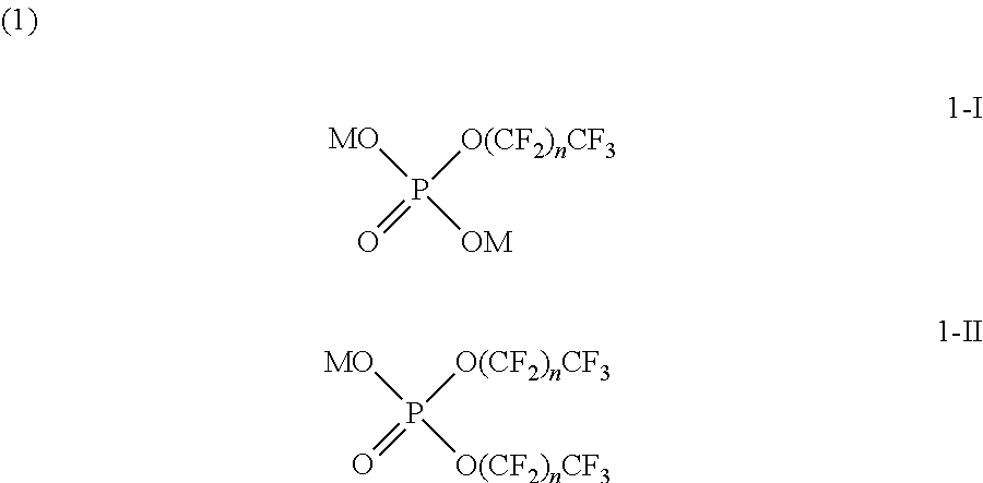
- the mixture of the perfluorinated phosphate salts may be an ester mixture containing a monoester salt having a structure of 1-I and a diester salt having a structure of 1-II represented by Formula 1:
- each n in Formula 1 is a natural number, preferably an integer ranging from 5 to 11. In a more specific embodiment, each n is 7. When each n is within the range defined above, low viscosity and flowability of the surfactant can be attained, achieving improved workability. In addition, the hydrophilicity and hydrophobicity of the surfactant are adjustable, ensuring good dispersibility and processing stability.
- each M is an alkali metal.
- the monoester salt accounts for 33 to 45% by weight of the total weight of the monoester salt and the diester salt. In the ester salt mixture, the ester salt components have an apparent average molecular weight of 560 to 980.
- the fluorinated surfactant is a perfluoroalkyl sulfate surfactant.
- the perfluoroalkyl sulfate is distinguished from a perfluoroalkyl sulfonate in that the perfluoroalkyl group is connected to the sulfur atom through the oxygen atom.
- the anionic surfactant there may also be used an ester of chlorosulfonic acid (ClSO 3 H) or sulfamic acid (NH 2 SO 3 H) and a perfluorinated alcohol or optionally an alkali salt of the ester.
- the perfluoroalkyl sulfate surfactant may be a sulfamate having a structure represented by Formula 2:
- n in Formula 2 is an integer from 5 to 11. In a more specific embodiment, n is 7.
- n is within the range defined above, low viscosity and flowability of the surfactant can be attained, achieving improved workability.
- the hydrophilicity and hydrophobicity of the surfactant are adjustable, ensuring good dispersibility and processing stability.
- the water content of the sulfamate surfactant may be from 30 to 90% by weight.
- the use of the sulfamate as the sulfuric acid-based surfactant is advantageous in that an ammonium salt as a charged ionic species (a protonated amino group) can be obtained with the perfluoroalkyl ester only. Due to this advantage, the use of the sulfamate can avoid the need for alkali treatment to enhance the hydrophilicity of the surfactant, unlike the use of sulfuric acid or chlorosulfuric acid.
- the fluorinated surfactant is a perfluoroalkyl sulfonate salt surfactant.
- the perfluoroalkyl sulfonate salt surfactant may have a structure represented by Formula 3:
- n in Formula 3 is a natural number, preferably an integer ranging from 5 to 11. In a more specific embodiment, n is 7.
- n is within the range defined above, low viscosity and flowability of the surfactant can be attained, achieving improved workability.
- hydrophilicity and hydrophobicity of the surfactant are adjustable, ensuring good dispersibility and processing stability.
- the fluorinated surfactant can exhibit dispersion, emulsification, and defoaming effects.
- the fluorinated surfactant functions to make the crystal of the plating metal fine, improving the grain size and shape characteristics of bumps.
- Other functions of the fluorinated surfactant are to reduce the height variations of bumps (WID and WIW) and to prevent the formation of empty spaces inside bumps and cracks in intermetallic layers.
- the fluorinated surfactant may be a commercially available product.
- the fluorinated surfactant 0.01 to 100 mg/L of the fluorinated surfactant is included in the tin-based electroplating solution.
- the content of the fluorinated surfactant may be adjusted to the range of 0.05 to 10 mg/L. Within this range, the tin-based crystal on the surface of bumps can be made fine, the height variation of bumps can be reduced, and the formation of empty spaces inside bumps and cracks in intermetallic layers can be prevented.
- the electroplating solution of the present invention may further include organic additives.
- the total concentration of the additives and the fluorinated surfactant is suitably adjusted to 10 to 100 g/L.
- the kinds of the organic additives suitable for use in the tin-based electroplating solution of the present invention may be determined by those skilled in the art according to the intended applications and detailed descriptions thereof are thus omitted herein.
- Examples of the organic additives include grain-refining agents, complexing agents, antioxidants, and defoaming agents.
- the electroplating solution of the present invention is preferably subjected to filtration before use for electroplating.
- the plating solution may be filtered through a cartridge filter having a pore size of several micrometers to remove precipitates or impurities.
- the pore size of the cartridge filter may be, for example, from 0.2 to 6 ⁇ m.
- a filter paper having a pore size of 0.2 to 6 ⁇ m may also be used.
- a further aspect of the present invention provides a method of producing solder bumps for a flip chip by using the tin-based electroplating solution.
- the method of the present invention involves the formation of copper-based metal pillars on an UBM layer and the plating of tin or tin-silver alloy solder bumps thereon.
- the tin-based electroplating solution is applied within 12 hours after copper or copper/nickel pillars are formed on an UBM layer.
- tin plating or tin-silver alloy plating may be performed in a continuous process. This continuous plating process within 12 hours can minimize the intermetallic adhesion resulting from the formation of oxide films on the copper or nickel surface or the occurrence of cracks and defects between the metal layers.
- the method of the present invention includes (A) electroplating a silicon wafer having a protective layer through which an electrode pad is exposed and an under bump metallurgy (UBM) layer with a copper or copper/nickel plating solution to form copper or copper/nickel pillars on the under bump metallurgy layer and (B) electroplating the pillars with the tin-based electroplating solution to form solder bumps.
- UBM under bump metallurgy
- the electroplating method for the formation of the copper or copper/nickel pillars on the under bump metallurgy layer and the copper or copper/nickel electroplating solution used in the electroplating method in step (A).
- the plating method and the plating solution may be those that are commonly used in the art.
- the copper electroplating solution may be one that includes copper sulfate, sulfuric acid (H 2 SO 4 ), hydrochloric acid, water, and optionally additives.
- the copper electroplating solution may be commercially available from JCU, Co., Ltd. (Japan) under the trade name Cu-BRITE BUHD.
- the tin-based electroplating for the formation of solder bumps in step (B) may be performed by any suitable process known in the art and thus specific conditions thereof are not described herein.
- the electroplating may be performed using a silicon wafer, as a cathode, formed with the copper pillars on the UBM layer and an inert metal electrode (e.g., a platinum electrode or platinum-coated electrode) as an anode.
- the electroplating for the formation of solder bumps in step (B) may be performed at a current density of 3 to 20 A/dm 2 .
- high speed plating is possible at a current density of 10 to 19 A/dm 2 .
- copper pillars were formed on a copper under bump metallurgy (UBM) layer of a flip chip semiconductor package.
- UBM copper under bump metallurgy
- a commercial copper sulfate-based electroplating solution containing CuSO 4 .5H 2 O, H 2 SO 4 , HCl, H 2 O, and organic additives (Cu-BRITE BUHD, JCU Co., Ltd., Japan) was plated on a 12-inch patterned wafer to form copper pillars.
- the copper electroplating was performed according to the manufacturer's recommendation and thus a brief explanation is herein given of the plating conditions.
- the plating solution was stirred at room temperature and plated at a current density of 10 A/dm 2 until the height of copper pillars reached 10 ⁇ m.
- FIG. 2 shows electron microscopy images of the copper pillars formed under the above conditions.
- Tin methanesulfonate (based on the final tin content (95 g/L)), silver methanesulfonate (based on the final silver content (2.0 g/L)), 100 g/L of methanesulfonic acid, 0.1 mg/L of potassium perfluorinated octyl sulfonate, 13.5 g/L of polyoxyethylenestyrenic phenyl ether, 1.5 g/L of polyoxyethylene bisphenol F ether, and 270 g/L of thiodiglycol as a complexing agent were mixed with stirring and filtered through a cartridge filter having a pore size of several micrometers to prepare a tin-silver alloy plating solution.
- galvanostatic plating was performed using the tin-silver alloy plating solution of Example 1 and the characteristics of the plated tin-silver alloy were evaluated.
- the cross section of a brass plate having a size of 2 ⁇ 2 cm 2 was used as a cathode and a platinum-coated titanium electrode was used as an anode.
- Galvanostatic plating was performed at current densities of 5 and 10 A/dm 2 while stirring 250 mL of the plating solution at a rate of 100 rpm until the thickness reached 20 ⁇ m. The results are shown in FIGS. 3 and 4 .
- the surface shapes of the tin-silver plated layers formed at current densities of 5 ASD and 10 ASD are shown in FIGS. 3 and 4 , respectively.
- Example 2 The tin-silver electroplating solution of Example 1 was electroplated on the copper pillars, which were formed on the 12-inch patterned wafer in Preparative Example 1, to form solder bumps.
- the tin-silver electroplating was performed at a current density of 13 A/dm 2 while stirring the plating solution at room temperature.
- the plating speed was 6.6 ⁇ m/min at 13 A/dm 2 .
- a current efficiency of 99.5% and a silver content of 2.2% were attained. After heating to 240° C. at a rate of 2° C./min and cooling at a rate of 3° C./min, solder reflow was performed.
- solder bumps were well patterned (bump CD 20-60 ⁇ m, bump pitch 95-190 ⁇ m) and the plating tendency was good regardless of the shape (pillar or mushroom shape) of the solder bumps. Meanwhile, tin-silver plating was performed at different current densities. The current efficiencies of the plating were found to be 99.6, 99.5, 99.5, 98.9, 98.0, and 95.8% at current densities of 10, 12, 13, 14, 15, and 16 A/dm 2 , respectively.
- the solder bumps obtained by plating at a current density of 13 A/dm 2 were analyzed by electron microscopy and X-ray imaging before and after the solder reflow. As a result, the bumps could be confirmed to have smooth surface appearances after the solder reflow.
- the variation between the maximum and minimum heights of the within die (WID) solder bumps was 19.79 ⁇ 0.19 ⁇ m.
- the proportion of silver in the tin-silver alloy was 2.2%, as measured by atomic absorption (AA) spectrophotometry.
- the X-ray imaging revealed that the solder bumps had a dense structure without empty spaces.
- Example 1 the shape and characteristics of tin-silver alloy bumps were observed.
- the tin-silver electroplating solution of Example 1 was electroplated on the 12-inch patterned wafer formed with the under bump metallurgy layer, which was prepared in Preparative Example 1, to form solder bumps.
- Example 3 was different from Evaluation Example 1 in that the plated patterned wafer used in Preparative Example 1 was cut into a test piece having a size of 3 ⁇ 3 cm 2 , which was used as a cathode, a platinum-coated titanium electrode was used as an anode, and galvanostatic plating was performed at current densities of 5 and 10 A/dm 2 while stirring 250 mL of the electroplating solution at a rate of 250 rpm until the thickness reached 20 ⁇ m. The characteristics of the solder bumps were measured and the results are shown in Table 2 and FIGS. 5 ( 5 a ) and 6 ( 6 a ).
- Solder bumps were formed by tin-silver plating in the same manner as in Example 3, except that the fluorinated surfactant component was excluded from the electroplating solution. The characteristics of the solder bumps formed at densities of 5 A/dm 2 and 10 A/dm 2 were measured. The results are shown in Table 2 and FIGS. 5 ( 5 b ) and 6 ( 6 B).
- Example 3 The compositions of the tin-based electroplating solutions used in Example 3 and Comparative Example 1 are summarized in Table 1.
- Example 1 Tin methanesulfonate Based on final tin The same as left concentration (95 g/L) Silver methanesulfonate Based on final silver The same as left concentration (2.0 g/L) Potassium perfluorinated 0.1 mg/L — octyl sulfonate Methanesulfonic acid 100 g/L The same as left Aromatic polyoxyalkylene POE-SPE 13.5 g/L The same as left ethers POE-BPF 1.5 g/L Thiodiglycol 270 g/L The same as left Water Remainder The same as left ⁇ POE-SPE: Polyoxyethylenestyrenic phenyl ether POE-BPF: Polyoxyethylene bisphenol F ether
- Example 3 To evaluate the appearances of the plating films obtained in Example 3 and Comparative Example 1, the shapes of the bumps before and after solder reflow were observed by SEM. The current efficiencies, silver contents (by atomic absorption spectrophotometry), empty spaces inside the bumps after reflow (by X-ray imaging), and WID values (%) were measured. The WID value was obtained by dividing the difference between the maximum and minimum heights of the within die (WID) bumps by the average height and was expressed in percent. The appearances of the bumps were relatively evaluated based on surface fineness and flatness.
- the bumps were judged to be “excellent” when there were no empty spaces inside the bumps, “good” when empty spaces were not larger than 0.05%, and “poor” when empty spaces were larger than 0.05%, as observed by X-ray imaging.
- the results are shown in Table 2 and FIG. 5 .
- FIGS. 5 ( 5 a ) and 6 ( 6 a ) show SEM images of the bumps formed using the plating solution including the fluorinated surfactant component at 5 ASD and 10 ASD, respectively.
- FIGS. 5 ASD and 10 ASD show SEM images of the bumps formed using the plating solution including the fluorinated surfactant component at 5 ASD and 10 ASD, respectively.
Landscapes
- Chemical & Material Sciences (AREA)
- Engineering & Computer Science (AREA)
- Chemical Kinetics & Catalysis (AREA)
- Electrochemistry (AREA)
- Materials Engineering (AREA)
- Metallurgy (AREA)
- Organic Chemistry (AREA)
- Crystallography & Structural Chemistry (AREA)
- Manufacturing & Machinery (AREA)
- Computer Hardware Design (AREA)
- Microelectronics & Electronic Packaging (AREA)
- Power Engineering (AREA)
- Electroplating And Plating Baths Therefor (AREA)
Abstract
Description


| TABLE 1 | ||
| Comparative | ||
| Component | Example 3 | Example 1 |
| Tin methanesulfonate | Based on final tin | The same as left |
| concentration (95 g/L) | ||
| Silver methanesulfonate | Based on final silver | The same as left |
| concentration (2.0 g/L) | ||
| Potassium perfluorinated | 0.1 mg/L | — |
| octyl sulfonate | ||
| Methanesulfonic acid | 100 g/L | The same as left |
| Aromatic polyoxyalkylene | POE-SPE 13.5 g/L | The same as left |
| ethers | POE-BPF 1.5 g/L | |
| Thiodiglycol | 270 g/L | The same as left |
| Water | Remainder | The same as left |
| ※ POE-SPE: Polyoxyethylenestyrenic phenyl ether | ||
| POE-BPF: Polyoxyethylene bisphenol F ether | ||
| TABLE 2 |
| Evaluation of the tin-silver alloy bumps formed at 10 ASD |
| Current | Silver | Average bump | Bump appearance | Empty spaces |
| Parameters | efficiency, % | content, % | thickness, μm | WID, % | Before reflow | After reflow | inside bumps after reflow |
| Example 3 | 98.2 | 2.2 | 21.18 | 0.62 | Excellent | Excellent | Excellent |
| Comparative | 97.1 | 2.7 | 21.70 | 5.0 | Excellent-good | Excellent-good | Good |
| Example 1 | |||||||
Claims (10)


Applications Claiming Priority (2)
| Application Number | Priority Date | Filing Date | Title |
|---|---|---|---|
| KR20140098394 | 2014-07-31 | ||
| KR10-2014-0098394 | 2014-07-31 |
Publications (2)
| Publication Number | Publication Date |
|---|---|
| US20160035685A1 US20160035685A1 (en) | 2016-02-04 |
| US9871010B2 true US9871010B2 (en) | 2018-01-16 |
Family
ID=55180823
Family Applications (1)
| Application Number | Title | Priority Date | Filing Date |
|---|---|---|---|
| US14/810,414 Active 2036-01-07 US9871010B2 (en) | 2014-07-31 | 2015-07-27 | Tin alloy electroplating solution for solder bumps including perfluoroalkyl surfactant |
Country Status (4)
| Country | Link |
|---|---|
| US (1) | US9871010B2 (en) |
| KR (1) | KR101636361B1 (en) |
| CN (1) | CN105316711B (en) |
| TW (1) | TWI575115B (en) |
Families Citing this family (6)
| Publication number | Priority date | Publication date | Assignee | Title |
|---|---|---|---|---|
| JP7009679B2 (en) * | 2015-07-29 | 2022-01-26 | 石原ケミカル株式会社 | Electric tin and electric tin alloy plating bath, method of forming electrodeposits using the plating bath |
| CN106757212B (en) * | 2016-11-30 | 2018-02-02 | 昆山成功环保科技有限公司 | ELECTROPLATING Sn-Ag ALLOY solution for wafer-level packaging |
| CN111690958B (en) * | 2019-03-15 | 2023-07-28 | 上海新阳半导体材料股份有限公司 | Tin plating solution, preparation method and application thereof |
| CN113652719B (en) * | 2021-08-13 | 2024-01-19 | 广西隆林利通线缆科技有限公司 | Electroplating solution for copper wire tinning and copper wire tinning method |
| CN117773409B (en) * | 2023-12-20 | 2024-09-03 | 道尔化成电子材料(上海)有限公司 | Nano silver-based composite solder and preparation method thereof |
| CN118639288B (en) * | 2024-08-12 | 2024-11-15 | 江苏中科智芯集成科技有限公司 | Tin-silver alloy bump and preparation method thereof |
Citations (3)
| Publication number | Priority date | Publication date | Assignee | Title |
|---|---|---|---|---|
| US4381228A (en) * | 1981-06-16 | 1983-04-26 | Occidental Chemical Corporation | Process and composition for the electrodeposition of tin and tin alloys |
| US20090145765A1 (en) * | 2007-12-11 | 2009-06-11 | Enthone Inc. | Composite coatings for whisker reduction |
| US20150308007A1 (en) * | 2014-04-28 | 2015-10-29 | Samsung Electronics Co., Ltd. | Tin plating solution, tin plating equipment, and method for fabricating semiconductor device using the tin plating solution |
Family Cites Families (11)
| Publication number | Priority date | Publication date | Assignee | Title |
|---|---|---|---|---|
| US6251249B1 (en) * | 1996-09-20 | 2001-06-26 | Atofina Chemicals, Inc. | Precious metal deposition composition and process |
| JP3334594B2 (en) * | 1998-02-16 | 2002-10-15 | 三菱マテリアル株式会社 | Plating bath and method for forming bump electrodes on semiconductor wafer |
| JP3455712B2 (en) * | 2000-04-14 | 2003-10-14 | 日本ニュークローム株式会社 | Pyrophosphate bath for copper-tin alloy plating |
| JP4698904B2 (en) * | 2001-09-20 | 2011-06-08 | 株式会社大和化成研究所 | Tin or tin-based alloy plating bath, tin salt and acid or complexing agent solution for building bath, maintenance or replenishment of the plating bath, and electric / electronic parts manufactured using the plating bath |
| JP2004276219A (en) * | 2003-03-18 | 2004-10-07 | Ebara Corp | Electrolytic machining liquid, electrolytic machining device, and wiring machining method |
| JP4758614B2 (en) * | 2003-04-07 | 2011-08-31 | ローム・アンド・ハース・エレクトロニック・マテリアルズ,エル.エル.シー. | Electroplating composition and method |
| CN100595342C (en) * | 2005-03-24 | 2010-03-24 | 肇庆市羚光电子化学品材料科技有限公司 | Additive for tin methanesulfonate-based pure tin electroplating solution |
| JP4812365B2 (en) * | 2005-08-19 | 2011-11-09 | ローム・アンド・ハース・エレクトロニック・マテリアルズ,エル.エル.シー. | Tin electroplating solution and tin electroplating method |
| ES2361500T3 (en) * | 2006-01-06 | 2011-06-17 | Enthone, Incorporated | ELECTROLYTE AND PROCEDURE FOR THE PRECIPITATION OF A MATE METAL LAYER. |
| EP2221396A1 (en) * | 2008-12-31 | 2010-08-25 | Rohm and Haas Electronic Materials LLC | Lead-Free Tin Alloy Electroplating Compositions and Methods |
| KR20150080398A (en) * | 2013-12-31 | 2015-07-09 | 주식회사 에이피씨티 | Method for Manufacturing Solder Bumps for Flip Chips and Metal Electroplating Solution for the Same |
-
2014
- 2014-11-10 KR KR1020140155735A patent/KR101636361B1/en active Active
-
2015
- 2015-07-24 TW TW104124104A patent/TWI575115B/en active
- 2015-07-27 US US14/810,414 patent/US9871010B2/en active Active
- 2015-07-30 CN CN201510458355.XA patent/CN105316711B/en active Active
Patent Citations (3)
| Publication number | Priority date | Publication date | Assignee | Title |
|---|---|---|---|---|
| US4381228A (en) * | 1981-06-16 | 1983-04-26 | Occidental Chemical Corporation | Process and composition for the electrodeposition of tin and tin alloys |
| US20090145765A1 (en) * | 2007-12-11 | 2009-06-11 | Enthone Inc. | Composite coatings for whisker reduction |
| US20150308007A1 (en) * | 2014-04-28 | 2015-10-29 | Samsung Electronics Co., Ltd. | Tin plating solution, tin plating equipment, and method for fabricating semiconductor device using the tin plating solution |
Also Published As
| Publication number | Publication date |
|---|---|
| CN105316711A (en) | 2016-02-10 |
| KR101636361B1 (en) | 2016-07-06 |
| TW201604334A (en) | 2016-02-01 |
| TWI575115B (en) | 2017-03-21 |
| KR20160018310A (en) | 2016-02-17 |
| CN105316711B (en) | 2018-01-05 |
| US20160035685A1 (en) | 2016-02-04 |
Similar Documents
| Publication | Publication Date | Title |
|---|---|---|
| US9871010B2 (en) | Tin alloy electroplating solution for solder bumps including perfluoroalkyl surfactant | |
| US7713859B2 (en) | Tin-silver solder bumping in electronics manufacture | |
| KR101361555B1 (en) | Tin electroplating bath, tin-plated coating film, tin electroplating method, and electronic device component | |
| KR101319863B1 (en) | Tin electroplating solution and tin electroplating method | |
| JP6198343B2 (en) | Non-cyanide electrolytic gold plating solution | |
| JP2015045094A (en) | Lead-free tin alloy electroplating compositions and methods | |
| JP6759736B2 (en) | Plating liquid | |
| US11840771B2 (en) | Composition for tin or tin alloy electroplating comprising suppressing agent | |
| KR101722703B1 (en) | Tin-silver solder bump plating solution | |
| JP2009191335A (en) | Plating solution and electronic parts | |
| KR20160033678A (en) | Method for Manufacturing Solder Bumps for Flip Chips and Metal Electroplating Solution for the Same | |
| JP2018009227A (en) | Electrolytic palladium silver alloy plating film and electrolytic plating solution for forming the same | |
| JP2017155296A (en) | Plating solution | |
| CN1638198A (en) | Terminal having surface layer ,and part and product having the same | |
| KR102533369B1 (en) | Tin-silver plating solution and method of forming tin-silver solder bumps using the same | |
| KR20210037046A (en) | SnAgCu electroplating solution for solder bump and solder bump manufactured by the same | |
| KR101596437B1 (en) | Method for Manufacturing Copper Pillars for Flip Chips and Copper-Based Electroplating Solution for the Same | |
| CN116848292A (en) | Tin alloy plating solution | |
| KR101738535B1 (en) | Tin-based electroplating solution for solder bump | |
| CN111690958B (en) | Tin plating solution, preparation method and application thereof | |
| KR20230029380A (en) | Sn-Ag electroplating solution for solder bump and manufacturing method of solder bump for flip chip using the same | |
| US20220316085A1 (en) | Structure including copper plating layer or copper alloy plating layer | |
| TWI805090B (en) | Tin-silver plating solution, method of forming tin-silver solder bump using same, and tin-silver solder bump formed by said forming method | |
| WO2022080191A1 (en) | Tin or tin alloy plating solution, and bump formation method which uses said plating solution | |
| KR102634249B1 (en) | Plating Composition and Method for Forming The Solder Bump |
Legal Events
| Date | Code | Title | Description |
|---|---|---|---|
| AS | Assignment |
Owner name: APCT CO., LTD, KOREA, REPUBLIC OF Free format text: ASSIGNMENT OF ASSIGNORS INTEREST;ASSIGNORS:KO, JUNG WOO;OH, JEONG HUN;PARK, KYU BIN;AND OTHERS;REEL/FRAME:036188/0499 Effective date: 20150722 |
|
| STCF | Information on status: patent grant |
Free format text: PATENTED CASE |
|
| MAFP | Maintenance fee payment |
Free format text: PAYMENT OF MAINTENANCE FEE, 4TH YR, SMALL ENTITY (ORIGINAL EVENT CODE: M2551); ENTITY STATUS OF PATENT OWNER: SMALL ENTITY Year of fee payment: 4 |
|
| MAFP | Maintenance fee payment |
Free format text: PAYMENT OF MAINTENANCE FEE, 8TH YR, SMALL ENTITY (ORIGINAL EVENT CODE: M2552); ENTITY STATUS OF PATENT OWNER: SMALL ENTITY Year of fee payment: 8 |