US9865953B2 - Electrical contact assembly for printed circuit boards - Google Patents
Electrical contact assembly for printed circuit boards Download PDFInfo
- Publication number
- US9865953B2 US9865953B2 US15/646,234 US201715646234A US9865953B2 US 9865953 B2 US9865953 B2 US 9865953B2 US 201715646234 A US201715646234 A US 201715646234A US 9865953 B2 US9865953 B2 US 9865953B2
- Authority
- US
- United States
- Prior art keywords
- socket
- contact region
- contact
- housing
- socket pin
- Prior art date
- Legal status (The legal status is an assumption and is not a legal conclusion. Google has not performed a legal analysis and makes no representation as to the accuracy of the status listed.)
- Active
Links
- 238000000034 method Methods 0.000 claims abstract description 25
- 230000008569 process Effects 0.000 claims abstract description 25
- 229910000679 solder Inorganic materials 0.000 claims abstract description 23
- 238000005452 bending Methods 0.000 claims description 18
- 238000009434 installation Methods 0.000 abstract description 8
- 230000014759 maintenance of location Effects 0.000 description 6
- 230000000712 assembly Effects 0.000 description 4
- 238000000429 assembly Methods 0.000 description 4
- 230000008901 benefit Effects 0.000 description 4
- 238000013459 approach Methods 0.000 description 3
- 230000009471 action Effects 0.000 description 2
- 230000006872 improvement Effects 0.000 description 2
- 238000005476 soldering Methods 0.000 description 2
- 230000002411 adverse Effects 0.000 description 1
- 230000004888 barrier function Effects 0.000 description 1
- 230000015572 biosynthetic process Effects 0.000 description 1
- 230000006835 compression Effects 0.000 description 1
- 238000007906 compression Methods 0.000 description 1
- 230000007547 defect Effects 0.000 description 1
- 230000000694 effects Effects 0.000 description 1
- 238000005755 formation reaction Methods 0.000 description 1
- 238000007689 inspection Methods 0.000 description 1
- 238000004519 manufacturing process Methods 0.000 description 1
- 239000000463 material Substances 0.000 description 1
- 238000010137 moulding (plastic) Methods 0.000 description 1
- 238000004806 packaging method and process Methods 0.000 description 1
- 239000002699 waste material Substances 0.000 description 1
Images


Classifications
-
- H—ELECTRICITY
- H01—ELECTRIC ELEMENTS
- H01R—ELECTRICALLY-CONDUCTIVE CONNECTIONS; STRUCTURAL ASSOCIATIONS OF A PLURALITY OF MUTUALLY-INSULATED ELECTRICAL CONNECTING ELEMENTS; COUPLING DEVICES; CURRENT COLLECTORS
- H01R12/00—Structural associations of a plurality of mutually-insulated electrical connecting elements, specially adapted for printed circuits, e.g. printed circuit boards [PCB], flat or ribbon cables, or like generally planar structures, e.g. terminal strips, terminal blocks; Coupling devices specially adapted for printed circuits, flat or ribbon cables, or like generally planar structures; Terminals specially adapted for contact with, or insertion into, printed circuits, flat or ribbon cables, or like generally planar structures
- H01R12/50—Fixed connections
- H01R12/51—Fixed connections for rigid printed circuits or like structures
- H01R12/55—Fixed connections for rigid printed circuits or like structures characterised by the terminals
- H01R12/57—Fixed connections for rigid printed circuits or like structures characterised by the terminals surface mounting terminals
-
- H—ELECTRICITY
- H01—ELECTRIC ELEMENTS
- H01R—ELECTRICALLY-CONDUCTIVE CONNECTIONS; STRUCTURAL ASSOCIATIONS OF A PLURALITY OF MUTUALLY-INSULATED ELECTRICAL CONNECTING ELEMENTS; COUPLING DEVICES; CURRENT COLLECTORS
- H01R13/00—Details of coupling devices of the kinds covered by groups H01R12/70 or H01R24/00 - H01R33/00
- H01R13/02—Contact members
- H01R13/10—Sockets for co-operation with pins or blades
- H01R13/11—Resilient sockets
-
- H—ELECTRICITY
- H01—ELECTRIC ELEMENTS
- H01R—ELECTRICALLY-CONDUCTIVE CONNECTIONS; STRUCTURAL ASSOCIATIONS OF A PLURALITY OF MUTUALLY-INSULATED ELECTRICAL CONNECTING ELEMENTS; COUPLING DEVICES; CURRENT COLLECTORS
- H01R12/00—Structural associations of a plurality of mutually-insulated electrical connecting elements, specially adapted for printed circuits, e.g. printed circuit boards [PCB], flat or ribbon cables, or like generally planar structures, e.g. terminal strips, terminal blocks; Coupling devices specially adapted for printed circuits, flat or ribbon cables, or like generally planar structures; Terminals specially adapted for contact with, or insertion into, printed circuits, flat or ribbon cables, or like generally planar structures
- H01R12/70—Coupling devices
- H01R12/71—Coupling devices for rigid printing circuits or like structures
- H01R12/712—Coupling devices for rigid printing circuits or like structures co-operating with the surface of the printed circuit or with a coupling device exclusively provided on the surface of the printed circuit
- H01R12/716—Coupling device provided on the PCB
-
- H—ELECTRICITY
- H01—ELECTRIC ELEMENTS
- H01R—ELECTRICALLY-CONDUCTIVE CONNECTIONS; STRUCTURAL ASSOCIATIONS OF A PLURALITY OF MUTUALLY-INSULATED ELECTRICAL CONNECTING ELEMENTS; COUPLING DEVICES; CURRENT COLLECTORS
- H01R43/00—Apparatus or processes specially adapted for manufacturing, assembling, maintaining, or repairing of line connectors or current collectors or for joining electric conductors
- H01R43/04—Apparatus or processes specially adapted for manufacturing, assembling, maintaining, or repairing of line connectors or current collectors or for joining electric conductors for forming connections by deformation, e.g. crimping tool
-
- H—ELECTRICITY
- H01—ELECTRIC ELEMENTS
- H01R—ELECTRICALLY-CONDUCTIVE CONNECTIONS; STRUCTURAL ASSOCIATIONS OF A PLURALITY OF MUTUALLY-INSULATED ELECTRICAL CONNECTING ELEMENTS; COUPLING DEVICES; CURRENT COLLECTORS
- H01R43/00—Apparatus or processes specially adapted for manufacturing, assembling, maintaining, or repairing of line connectors or current collectors or for joining electric conductors
- H01R43/20—Apparatus or processes specially adapted for manufacturing, assembling, maintaining, or repairing of line connectors or current collectors or for joining electric conductors for assembling or disassembling contact members with insulating base, case or sleeve
- H01R43/205—Apparatus or processes specially adapted for manufacturing, assembling, maintaining, or repairing of line connectors or current collectors or for joining electric conductors for assembling or disassembling contact members with insulating base, case or sleeve with a panel or printed circuit board
-
- H—ELECTRICITY
- H05—ELECTRIC TECHNIQUES NOT OTHERWISE PROVIDED FOR
- H05K—PRINTED CIRCUITS; CASINGS OR CONSTRUCTIONAL DETAILS OF ELECTRIC APPARATUS; MANUFACTURE OF ASSEMBLAGES OF ELECTRICAL COMPONENTS
- H05K3/00—Apparatus or processes for manufacturing printed circuits
- H05K3/30—Assembling printed circuits with electric components, e.g. with resistor
- H05K3/32—Assembling printed circuits with electric components, e.g. with resistor electrically connecting electric components or wires to printed circuits
- H05K3/34—Assembling printed circuits with electric components, e.g. with resistor electrically connecting electric components or wires to printed circuits by soldering
- H05K3/3447—Lead-in-hole components
-
- H—ELECTRICITY
- H05—ELECTRIC TECHNIQUES NOT OTHERWISE PROVIDED FOR
- H05K—PRINTED CIRCUITS; CASINGS OR CONSTRUCTIONAL DETAILS OF ELECTRIC APPARATUS; MANUFACTURE OF ASSEMBLAGES OF ELECTRICAL COMPONENTS
- H05K7/00—Constructional details common to different types of electric apparatus
- H05K7/02—Arrangements of circuit components or wiring on supporting structure
- H05K7/10—Plug-in assemblages of components, e.g. IC sockets
- H05K7/1053—Plug-in assemblages of components, e.g. IC sockets having interior leads
- H05K7/1061—Plug-in assemblages of components, e.g. IC sockets having interior leads co-operating by abutting
- H05K7/1069—Plug-in assemblages of components, e.g. IC sockets having interior leads co-operating by abutting with spring contact pieces
-
- H—ELECTRICITY
- H05—ELECTRIC TECHNIQUES NOT OTHERWISE PROVIDED FOR
- H05K—PRINTED CIRCUITS; CASINGS OR CONSTRUCTIONAL DETAILS OF ELECTRIC APPARATUS; MANUFACTURE OF ASSEMBLAGES OF ELECTRICAL COMPONENTS
- H05K1/00—Printed circuits
- H05K1/18—Printed circuits structurally associated with non-printed electric components
- H05K1/182—Printed circuits structurally associated with non-printed electric components associated with components mounted in the printed circuit board, e.g. insert mounted components [IMC]
- H05K1/184—Components including terminals inserted in holes through the printed circuit board and connected to printed contacts on the walls of the holes or at the edges thereof or protruding over or into the holes
-
- H—ELECTRICITY
- H05—ELECTRIC TECHNIQUES NOT OTHERWISE PROVIDED FOR
- H05K—PRINTED CIRCUITS; CASINGS OR CONSTRUCTIONAL DETAILS OF ELECTRIC APPARATUS; MANUFACTURE OF ASSEMBLAGES OF ELECTRICAL COMPONENTS
- H05K2201/00—Indexing scheme relating to printed circuits covered by H05K1/00
- H05K2201/10—Details of components or other objects attached to or integrated in a printed circuit board
- H05K2201/10227—Other objects, e.g. metallic pieces
- H05K2201/10295—Metallic connector elements partly mounted in a hole of the PCB
- H05K2201/10303—Pin-in-hole mounted pins
-
- H—ELECTRICITY
- H05—ELECTRIC TECHNIQUES NOT OTHERWISE PROVIDED FOR
- H05K—PRINTED CIRCUITS; CASINGS OR CONSTRUCTIONAL DETAILS OF ELECTRIC APPARATUS; MANUFACTURE OF ASSEMBLAGES OF ELECTRICAL COMPONENTS
- H05K2201/00—Indexing scheme relating to printed circuits covered by H05K1/00
- H05K2201/10—Details of components or other objects attached to or integrated in a printed circuit board
- H05K2201/10613—Details of electrical connections of non-printed components, e.g. special leads
- H05K2201/10621—Components characterised by their electrical contacts
- H05K2201/10704—Pin grid array [PGA]
-
- H—ELECTRICITY
- H05—ELECTRIC TECHNIQUES NOT OTHERWISE PROVIDED FOR
- H05K—PRINTED CIRCUITS; CASINGS OR CONSTRUCTIONAL DETAILS OF ELECTRIC APPARATUS; MANUFACTURE OF ASSEMBLAGES OF ELECTRICAL COMPONENTS
- H05K2201/00—Indexing scheme relating to printed circuits covered by H05K1/00
- H05K2201/10—Details of components or other objects attached to or integrated in a printed circuit board
- H05K2201/10613—Details of electrical connections of non-printed components, e.g. special leads
- H05K2201/10742—Details of leads
- H05K2201/1075—Shape details
- H05K2201/1078—Leads having locally deformed portion, e.g. for retention
-
- H—ELECTRICITY
- H05—ELECTRIC TECHNIQUES NOT OTHERWISE PROVIDED FOR
- H05K—PRINTED CIRCUITS; CASINGS OR CONSTRUCTIONAL DETAILS OF ELECTRIC APPARATUS; MANUFACTURE OF ASSEMBLAGES OF ELECTRICAL COMPONENTS
- H05K2201/00—Indexing scheme relating to printed circuits covered by H05K1/00
- H05K2201/10—Details of components or other objects attached to or integrated in a printed circuit board
- H05K2201/10613—Details of electrical connections of non-printed components, e.g. special leads
- H05K2201/10742—Details of leads
- H05K2201/1075—Shape details
- H05K2201/10803—Tapered leads, i.e. leads having changing width or diameter
Definitions
- the present invention relates generally to the field of electrical contacts, and more particularly to electrical contact assemblies.
- a land grid array is a type of surface-mount packaging for integrated circuits that is notable for having the pins on the socket rather than the integrated circuit.
- An LGA can be electrically connected to a printed circuit board either by the use of a socket or by soldering directly to the board.
- a CPU (central processing unit) socket is a mechanical component that provides mechanical and electrical connections between an integrated circuit and a printed circuit board.
- the CPU socket allows the integrated circuit to be placed and replaced without soldering.
- LGA sockets are typically used for integrated circuits having a large number of pins.
- the LGA socket design provides for a compression force to be applied once a surface plate is in position. Thus, providing mechanical retention while avoiding the risk of bending pins when inserting the integrated circuit into the socket.
- An aspect of the present invention is an assembly process including inserting a socket pin into a socket housing, the socket pin having a contact region, the socket housing having a rectangular contact cavity that receive the contact region, the contact region passing through the rectangular contact cavity and extending beyond the socket housing; bending the socket pin such that the contact region is configured to receive a solder ball including securing the socket housing, striking the contact region in a first direction, and striking the contact region a second direction such that the contact region is bent more than 90 degrees from an original orientation; and attaching the solder ball to the contact region.
- the contact region is bounded by an end of the socket pin and a stress concentration feature. The socket pin bends at the stress concentration feature.
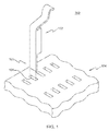
- FIG. 1 is an exploded view of a socket assembly according to an embodiment of the present invention
- FIG. 2 is a cut-away side view of a sub-assembly of a socket assembly according to an embodiment of the present invention
- FIG. 3 is a cut-away side view of a sub-assembly of a socket assembly according to an embodiment of the present invention
- FIGS. 4A and 4B are detail views of a socket pin used in the socket assembly of FIG. 1 ;
- FIG. 5 is a flowchart depicting an assembly process according to an embodiment of the present invention.
- an unresolved failure mode in the field of CPU sockets is the backing out of contacts during assembly caused by forces applied in a direction opposite the installation direction;
- conventional approaches provide for contact geometry to press into a pre-formed contact cavity in the socket housing;
- precision contact formations such as barbs and latches are stamped into the contacts, which increase design complexity and drive inefficient inspection processes and waste;
- conventional approaches to CPU socket design and assembly have an adverse effect on co-planarity among contacts on a single housing;
- each contact is pressed into place, but variations in the materials and other slight variations result in uneven solder ball contact locations, which results in sunken solder balls and electrical inconsistencies; and/or (vi) damaged solder balls cause solder defects during surface mount processing.
- Some embodiments of the present invention approach the problem of co-planarity by applying a final form process to the contact after installation into the socket housing.
- Some embodiment of the present invention solve the problem on backed out pins by a final forming process after installation of the contact into the socket housing.
- the final form operates to prevent the contact from backing out.
- a socket housing and contact assembly process includes forming the solder ball contact region after initial installation of a set of contacts into the housing.
- the contact regions of the set of contacts pass through corresponding contact cavities to extend beyond the housing and the contact regions are formed over at equal angles for solder ball placement.
- socket assembly 100 includes socket pin 102 and housing 104 .
- the housing and contact are illustrated in a simplified manner to emphasize aspects of the present invention for this disclosure.
- the housing includes additional structure to support the socket pin and prevent electrical shorting, such as dielectric barriers surrounding the mid-section of the contact, additional housing elements to protect from incidental contact with the cantilever contact portion, and/or housing elements configured to receive conventional contact retention features.
- the socket pin in some embodiments, may include conventional retention structure(s), such as barbs and/or latches, as discussed above.
- retention structures may be designed for lighter duty, that is, the retention structure may be used to hold the socket pin in place during assembly, but the fully formed socket assembly ( FIG. 3 ) is designed to be secure against back-out forces.
- Socket pin 102 includes a contact region 108 .
- the contact region is an area on the socket pin where socket assembly 100 is attached to a solder ball (not shown).
- the contact region is configured to pass through contact cavity 106 and protrude away from housing 104 . Further, the contact region is configured to receive the solder ball for subsequent assembly processing.
- socket assembly 100 is shown with socket pin 102 inserted into housing 104 .
- the side of housing 104 from which contact region 108 protrudes is attachment plane 202 .
- the distance that the contact region protrudes from the housing depends largely on the application.
- the corresponding solder ball (not shown) is approximately 0.6 mm and the contact region is 2 mm.
- a typical LGA socket assembly includes a contact region ranging from 1 mm to 3 mm. A person of ordinary skill in the art will be able to determine an appropriate length when designing the socket assembly.
- the depth of contact cavity 106 is a designer's choice. It should be noted that in this example design the depth of the contact cavity and the length of contact region 108 combine to the length of the unformed pin. In some embodiments, the depth of the contact cavity corresponds also to pin features, such as retention barbs and/or latches.
- Assembly rib 204 also referred to as a standoff, is an additional feature of housing 104 designed to support a forming process that is discussed in the following paragraphs with respect to FIG. 3 .
- socket assembly 200 is created by bending contact region 108 of socket assembly 100 .
- conventional socket assembly processes do not form, or bend, a contact region after the socket pin is installed into the housing.
- the contact region is bent over to establish a surface on which a solder ball is attached.
- the contact cavity is configured to block and/or restrict movement of the socket pin after forming the contact region. That is, the attachment surface and/or the assembly rib prevent movement of the pin opposite the installation direction after the forming operation.
- the simplified geometry of the contact cavity provides for a more uniform housing geometry, thus improving mold flow and reducing warpage performance over conventional socket assemblies.
- a roller strikes the contact region with a single striking action to form it over toward the housing.
- the striking action occurs in two stages, one stage to create an initial bend and a second stage to over-bend the contact to account for mechanical spring back.
- the assembly 100 is secured in a die (not shown) and a mechanical roller (not shown) bends a row of contact regions in a single motion along a planar direction.
- the roller moves out of plane just after passing the location of the assembly rib 204 to account for spring back of the contact regions.
- the assembly rib provides support for the contact region to be bent greater than 90 degrees toward the attachment plane 202 . It should be understood that when a contact region is bent over during contact with a roller moving in a planar direction, subsequent to the bending operation, the contact region will spring back somewhat in the opposing direction. By moving the roller, for example, out of plane toward the attachment plane, the contact region may be precisely bent for consistent and level solder ball attachment.
- rigid plates strike the bent contact region by moving out of plane for the final form.
- the plate may be set at a desired angle to account for spring back.
- the forming process may include repeated strikes by the rigid plates to establish the desired bend angle.
- FIGS. 4A and 4B additional features are presented to support both consistent bending of the contact region at a desired bending point and a reduced force requirement for the bending operation.
- One advantage provided by additional features as shown in FIGS. 4A and 4B are the reduced spring back tendency of the contact region.
- the illustrated features are different solutions drawing from the principle of stress concentration. By creating a stress concentration at a particular location on the contact, when a bending for is applied near the contact region, a failure will occur first at that location.
- FIG. 4A is a side view of contact region 408 a having notch 402 , or scoreline, located at a desired bend location. Effectively, contact region 408 a is located below the notch. When bending force is applied, whether by roller as described above, or by other application of force, contact region 408 a is bent over such that it remains approximately 90 degrees from its original orientation.
- FIG. 4B is a front view of contact region 408 b having a reduced width 404 that creates a region of less resistance to bending.
- contact region 408 b defined at one end by the reduced width, bends over such that it remains approximately 90 degrees from its original orientation.
- FIG. 5 is flowchart 500 for creating socket assembly 200 as shown in part at FIG. 3 .
- Step S 502 a set of socket pins are received along with a socket housing suitable for the installation of the socket pins.
- the socket pins are fully stamped and/or formed with the exception of a final bend to be made at a later step during the assembly process ( FIG. 1 ).
- the socket pins include a contact region, such as region 108 , and the socket housing includes a contact cavity, such as contact cavity 106 .
- step S 504 the set of socket pins are inserted into the housing as shown in part at FIG. 2 .
- the housing is configured to hold the socket pin in place, at least with sufficient resistance to movement to support bending the contact region.
- This resistance to movement includes resistance to backout forces and angular forces generated during the bending process.
- Resistance to movement during use of the socket is conventionally achieved with features such as barbs and/or latches on the socket pin that interact with the housing to secure the socket pin with respect to the housing. While the resistance to movement during bending is lower than in conventional designs where backout forces must be resisted during use, conventional barbs and/or latches may be used while practicing embodiments of the present invention.
- Resistance to angular movement is achieved with conventional housing geometry supporting the socket pin along the length of the pin.
- step S 506 the contact regions, extending below attachment surface 202 ( FIG. 2 ) are formed over such that they are oriented for the attachment of solder balls, one per contact region.
- the housing is advantageously designed with relatively simple rectangular through-hole cavities. Alternative geometries are envisioned, but not illustrated herein.
- One advantage that may be found in this design is the uniform wall thickness from one cavity length to a next cavity length. Additionally, the gap between cavity lengths may be designed to be equivalent to the thickness of the cavities.
- step S 508 solder balls are placed on the various contact regions.
- the contact regions are generally parallel with attachment plane 202 and are generally co-planar with one another where the bending process assures uniform application of bending force.
- the socket assemblies having installed solder balls, are ready for an infrared reflow process used during subsequent installation of the socket assemblies. While the examples provided show a 90 degree bend and discuss parallel configuration with respect to the attachment plane, the application of bending a contact region post-assembly may be applied to various shapes and directions.
- Some embodiments of the present invention may include one, or more, of the following features, characteristics and/or advantages: improved dynamic warpage performance; and relatively low housing mold tooling cost compared to conventional mold tooling.
- Some embodiments of the present invention are useful in CPU socket design where solder balls are attached to a contact surface.
- Technical problems that arise in CPU socket manufacturing include: damaged solder balls; solder ball co-planarity; and warpage of socket housing during surface mount processing.
- a contact forming process includes post assembly forming.
- the housing geometry is simplified, as shown, for example, in contact cavity 106 ( FIG. 1 ) as a rectangular shape.
- the simplified geometry may include fewer cored out features in the molded part than is required when installing the fully-formed contact.
Landscapes
- Engineering & Computer Science (AREA)
- Manufacturing & Machinery (AREA)
- Microelectronics & Electronic Packaging (AREA)
- Connecting Device With Holders (AREA)
- Coupling Device And Connection With Printed Circuit (AREA)
Abstract
Description
Claims (7)
Priority Applications (1)
| Application Number | Priority Date | Filing Date | Title |
|---|---|---|---|
| US15/646,234 US9865953B2 (en) | 2016-03-04 | 2017-07-11 | Electrical contact assembly for printed circuit boards |
Applications Claiming Priority (2)
| Application Number | Priority Date | Filing Date | Title |
|---|---|---|---|
| US15/060,728 US9793634B2 (en) | 2016-03-04 | 2016-03-04 | Electrical contact assembly for printed circuit boards |
| US15/646,234 US9865953B2 (en) | 2016-03-04 | 2017-07-11 | Electrical contact assembly for printed circuit boards |
Related Parent Applications (1)
| Application Number | Title | Priority Date | Filing Date |
|---|---|---|---|
| US15/060,728 Continuation US9793634B2 (en) | 2016-03-04 | 2016-03-04 | Electrical contact assembly for printed circuit boards |
Publications (2)
| Publication Number | Publication Date |
|---|---|
| US20170310031A1 US20170310031A1 (en) | 2017-10-26 |
| US9865953B2 true US9865953B2 (en) | 2018-01-09 |
Family
ID=59724364
Family Applications (2)
| Application Number | Title | Priority Date | Filing Date |
|---|---|---|---|
| US15/060,728 Active US9793634B2 (en) | 2016-03-04 | 2016-03-04 | Electrical contact assembly for printed circuit boards |
| US15/646,234 Active US9865953B2 (en) | 2016-03-04 | 2017-07-11 | Electrical contact assembly for printed circuit boards |
Family Applications Before (1)
| Application Number | Title | Priority Date | Filing Date |
|---|---|---|---|
| US15/060,728 Active US9793634B2 (en) | 2016-03-04 | 2016-03-04 | Electrical contact assembly for printed circuit boards |
Country Status (1)
| Country | Link |
|---|---|
| US (2) | US9793634B2 (en) |
Families Citing this family (2)
| Publication number | Priority date | Publication date | Assignee | Title |
|---|---|---|---|---|
| EP3633829B1 (en) * | 2018-10-01 | 2023-12-20 | Vitesco Technologies GmbH | Motor control unit for an electric motor, motor assembly and process for assembling a motor assembly |
| US10886647B2 (en) | 2018-11-27 | 2021-01-05 | International Business Machines Corporation | Electronic circuitry socket structure |
Citations (55)
| Publication number | Priority date | Publication date | Assignee | Title |
|---|---|---|---|---|
| US891039A (en) | 1907-12-10 | 1908-06-16 | Charles W Clifford | Electrical contact terminal. |
| US2293606A (en) | 1939-04-08 | 1942-08-18 | United Carr Fastener Corp | Contact terminal |
| US2962692A (en) | 1957-05-02 | 1960-11-29 | North American Aviation Inc | Electric contact terminal |
| US3201744A (en) | 1961-02-15 | 1965-08-17 | Itt | Contact terminal for an electrical conductor member |
| US4262984A (en) | 1978-07-19 | 1981-04-21 | Yamaichi Electric Mfg. Co., Ltd. | Electric contact terminal member |
| US4645114A (en) | 1985-06-17 | 1987-02-24 | Northern Telecom Limited | Shaped solder pad for surface mounting electronic devices and a surface mounting position incorporating such shaped pads |
| US4834681A (en) | 1987-09-28 | 1989-05-30 | Francelco | Electric contact terminal |
| US4851614A (en) | 1987-05-22 | 1989-07-25 | Compaq Computer Corporation | Non-occluding mounting hole with solder pad for printed circuit boards |
| US4950186A (en) | 1988-12-16 | 1990-08-21 | Amp Incorporated | Electrical contact terminal |
| US5284447A (en) | 1993-03-29 | 1994-02-08 | Virginia Plastics Company, Inc. | Contact terminal for modular plug |
| US5307980A (en) | 1993-02-10 | 1994-05-03 | Ford Motor Company | Solder pad configuration for wave soldering |
| WO1996005713A1 (en) | 1994-08-10 | 1996-02-22 | Ast Research, Inc. | Solder pad for printed circuit boards |
| US5543583A (en) | 1994-10-31 | 1996-08-06 | Motorola, Inc. | Conductive solder pad for bonding an electronic device to a ceramic substrate |
| US5779502A (en) | 1995-06-06 | 1998-07-14 | Ast Research | Socket integrating high frequency capacitor assembly |
| US5984693A (en) | 1998-12-17 | 1999-11-16 | Hon Hai Precision Ind. Co., Ltd. | Contact of an LGA socket |
| US6007365A (en) | 1996-11-26 | 1999-12-28 | Sumitomo Wiring Systems, Ltd. | Pressure contact terminal fitting |
| US6206721B1 (en) | 1998-03-20 | 2001-03-27 | Yazaki Corporation | Pressure contact terminal having multiple width wire cutting edges |
| US6292372B1 (en) | 1999-07-15 | 2001-09-18 | Lucent Technologies, Inc. | Solder thieving pad for wave soldered through-hole components |
| US6317323B1 (en) | 1999-11-02 | 2001-11-13 | Foxconn Precision Components Co., Ltd. | Heat sink assembly for an electrical socket |
| US20020071935A1 (en) | 2000-12-12 | 2002-06-13 | Chi-Chuan Wu | Passive element solder pad free of solder ball |
| US6413111B1 (en) | 2001-12-07 | 2002-07-02 | Hon Hai Precision Ind. Co., Ltd. | Pick up cap used for an electrical socket |
| US6478588B1 (en) | 2001-12-28 | 2002-11-12 | Hon Hai Precision Ind. Co., Ltd. | CPU socket assembly with pick up cap |
| US6494748B1 (en) | 1999-11-16 | 2002-12-17 | Yazaki Corporation | Butt type contact terminal |
| US6537097B1 (en) | 2001-12-14 | 2003-03-25 | Hon Hai Precision Ind. Co., Ltd. | Device for CPU socket actuation |
| US6561831B1 (en) | 2001-12-27 | 2003-05-13 | Hon Hai Precision Ind. Co., Ltd. | Housing of socket connector and conductive terminal thereof |
| EP1416780A2 (en) | 2002-10-31 | 2004-05-06 | Tyco Electronics AMP K.K. | LGA package socket |
| US6740576B1 (en) | 2000-10-13 | 2004-05-25 | Bridge Semiconductor Corporation | Method of making a contact terminal with a plated metal peripheral sidewall portion for a semiconductor chip assembly |
| US20040099716A1 (en) | 2002-11-27 | 2004-05-27 | Motorola Inc. | Solder joint reliability by changing solder pad surface from flat to convex shape |
| US6752635B1 (en) | 2003-03-31 | 2004-06-22 | Intel Corporation | Comb-shaped land grid array (LGA) socket contact for improved power delivery |
| US20040127085A1 (en) | 2002-10-18 | 2004-07-01 | James Chen | Connector for a pin grid array integrated circuit device |
| US6821127B2 (en) | 2002-04-12 | 2004-11-23 | Hon Hai Precision Ind. Co., Ltd | Socket assembly with vacuum pickup cap |
| US20050042852A1 (en) | 2003-08-19 | 2005-02-24 | Unitech Printed Circuit Board Corp. | Method for applying solder mask onto pad spacings of a printed circuit board |
| US6905377B2 (en) | 2002-09-17 | 2005-06-14 | Tyco Electronics Corporation | Contact for land grid array socket |
| US6927492B2 (en) | 2001-04-23 | 2005-08-09 | Shipley Company, L.L.C. | Solder pads and method of making a solder pad |
| US20060019508A1 (en) | 2004-04-27 | 2006-01-26 | Ronmee Industrial Corporation | Terminal formation for socket employed on CPU |
| US7037122B1 (en) | 2005-03-21 | 2006-05-02 | Giga-Byte Technology Co., Ltd. | CPU socket module and protective cap thereof |
| US7059869B2 (en) | 2004-02-27 | 2006-06-13 | Tyco Electronics Corporation | Metal contact LGA socket |
| US7104827B1 (en) | 2005-12-09 | 2006-09-12 | Huang-Chou Huang | CPU socket with multiple contacting tab holders |
| US7112068B2 (en) | 2004-06-30 | 2006-09-26 | Hon Hai Precision Inc. Co., Ltd. | Land grid array socket having contact-protecting mechanism |
| US20070281507A1 (en) | 2006-06-05 | 2007-12-06 | Hon Hai Precision Ind. Co., Ltd. | IC contact for LGA socket |
| US7578684B2 (en) | 2006-12-18 | 2009-08-25 | Hon Hai Precision Ind. Co., Ltd. | Socket assembly having a vacuum pickup cap |
| US7695288B2 (en) | 2008-06-25 | 2010-04-13 | Intel Corporation | Land grid array (LGA) socket with cells and method of fabrication and assembly |
| US7746655B1 (en) | 2008-12-16 | 2010-06-29 | Dell Products L.P. | System and method for assembly of a processor and socket on an information handling system printed circuit board |
| US7794236B2 (en) | 2008-12-15 | 2010-09-14 | Intel Corporation | Land grid array (LGA) socket for various package sizes |
| CN1838251B (en) | 2005-01-13 | 2010-10-13 | 日立环球储存科技荷兰有限公司 | Apparatus and method for reducing solder pad size in an electrical lead suspension |
| US7866985B2 (en) | 2008-01-22 | 2011-01-11 | Hon Hai Precision Ind. Co., Ltd. | CPU socket assembly with package retention mechanism |
| US7968141B2 (en) | 2001-12-13 | 2011-06-28 | Luvata Oy | Method for producing contact terminal with textured surface and use thereof |
| US7988459B2 (en) | 2009-06-30 | 2011-08-02 | Intel Corporation | Unified retention mechanism for CPU/socket loading and thermal solution attach |
| WO2012050236A1 (en) | 2010-10-14 | 2012-04-19 | Yazaki Corporation | Water proof press contact terminal and method for forming water proof press contact terminal |
| US8167630B2 (en) | 1996-10-10 | 2012-05-01 | Fci Americas Technology Llc | High density connector and method of manufacture |
| US20130059486A1 (en) | 2011-09-06 | 2013-03-07 | Samsung Electronics Co., Ltd. | Contact terminal for printed circuit board |
| US8461455B2 (en) | 2010-04-28 | 2013-06-11 | Joinset Co., Ltd. | Elastic electric contact terminal |
| US20140179175A1 (en) | 2012-12-24 | 2014-06-26 | Chief Land Electronic Co., Ltd. | Asymmetrical contact terminal and fabrication method of the same |
| US20140206206A1 (en) | 2013-01-21 | 2014-07-24 | International Business Machines Corporation | Land grid array (lga) socket cartridge and method of forming |
| US9069149B2 (en) * | 2013-03-15 | 2015-06-30 | Commscope, Inc. Of North Carolina | Flexible switch pack |
Family Cites Families (3)
| Publication number | Priority date | Publication date | Assignee | Title |
|---|---|---|---|---|
| US6193567B1 (en) * | 1999-09-27 | 2001-02-27 | Delphi Technologies, Inc. | Female terminal for printed circuit board |
| DE10009215C1 (en) * | 2000-02-26 | 2001-05-10 | Harting Kgaa | Surface-mounted plug-in connector for printed circuit board has contact elements with pin contacts at one end and solder connection terminals at opposite end bent through 90 degrees |
| TWM391761U (en) * | 2010-04-09 | 2010-11-01 | Hon Hai Prec Ind Co Ltd | Electrical connector |
-
2016
- 2016-03-04 US US15/060,728 patent/US9793634B2/en active Active
-
2017
- 2017-07-11 US US15/646,234 patent/US9865953B2/en active Active
Patent Citations (57)
| Publication number | Priority date | Publication date | Assignee | Title |
|---|---|---|---|---|
| US891039A (en) | 1907-12-10 | 1908-06-16 | Charles W Clifford | Electrical contact terminal. |
| US2293606A (en) | 1939-04-08 | 1942-08-18 | United Carr Fastener Corp | Contact terminal |
| US2962692A (en) | 1957-05-02 | 1960-11-29 | North American Aviation Inc | Electric contact terminal |
| US3201744A (en) | 1961-02-15 | 1965-08-17 | Itt | Contact terminal for an electrical conductor member |
| US4262984A (en) | 1978-07-19 | 1981-04-21 | Yamaichi Electric Mfg. Co., Ltd. | Electric contact terminal member |
| US4645114A (en) | 1985-06-17 | 1987-02-24 | Northern Telecom Limited | Shaped solder pad for surface mounting electronic devices and a surface mounting position incorporating such shaped pads |
| US4851614A (en) | 1987-05-22 | 1989-07-25 | Compaq Computer Corporation | Non-occluding mounting hole with solder pad for printed circuit boards |
| US4834681A (en) | 1987-09-28 | 1989-05-30 | Francelco | Electric contact terminal |
| US4950186A (en) | 1988-12-16 | 1990-08-21 | Amp Incorporated | Electrical contact terminal |
| US5307980A (en) | 1993-02-10 | 1994-05-03 | Ford Motor Company | Solder pad configuration for wave soldering |
| US5284447A (en) | 1993-03-29 | 1994-02-08 | Virginia Plastics Company, Inc. | Contact terminal for modular plug |
| WO1996005713A1 (en) | 1994-08-10 | 1996-02-22 | Ast Research, Inc. | Solder pad for printed circuit boards |
| US5543583A (en) | 1994-10-31 | 1996-08-06 | Motorola, Inc. | Conductive solder pad for bonding an electronic device to a ceramic substrate |
| US5779502A (en) | 1995-06-06 | 1998-07-14 | Ast Research | Socket integrating high frequency capacitor assembly |
| US8167630B2 (en) | 1996-10-10 | 2012-05-01 | Fci Americas Technology Llc | High density connector and method of manufacture |
| US6007365A (en) | 1996-11-26 | 1999-12-28 | Sumitomo Wiring Systems, Ltd. | Pressure contact terminal fitting |
| US6206721B1 (en) | 1998-03-20 | 2001-03-27 | Yazaki Corporation | Pressure contact terminal having multiple width wire cutting edges |
| US5984693A (en) | 1998-12-17 | 1999-11-16 | Hon Hai Precision Ind. Co., Ltd. | Contact of an LGA socket |
| US6292372B1 (en) | 1999-07-15 | 2001-09-18 | Lucent Technologies, Inc. | Solder thieving pad for wave soldered through-hole components |
| US6317323B1 (en) | 1999-11-02 | 2001-11-13 | Foxconn Precision Components Co., Ltd. | Heat sink assembly for an electrical socket |
| US6494748B1 (en) | 1999-11-16 | 2002-12-17 | Yazaki Corporation | Butt type contact terminal |
| US6740576B1 (en) | 2000-10-13 | 2004-05-25 | Bridge Semiconductor Corporation | Method of making a contact terminal with a plated metal peripheral sidewall portion for a semiconductor chip assembly |
| US20020071935A1 (en) | 2000-12-12 | 2002-06-13 | Chi-Chuan Wu | Passive element solder pad free of solder ball |
| US6927492B2 (en) | 2001-04-23 | 2005-08-09 | Shipley Company, L.L.C. | Solder pads and method of making a solder pad |
| US6413111B1 (en) | 2001-12-07 | 2002-07-02 | Hon Hai Precision Ind. Co., Ltd. | Pick up cap used for an electrical socket |
| US7968141B2 (en) | 2001-12-13 | 2011-06-28 | Luvata Oy | Method for producing contact terminal with textured surface and use thereof |
| US6537097B1 (en) | 2001-12-14 | 2003-03-25 | Hon Hai Precision Ind. Co., Ltd. | Device for CPU socket actuation |
| US6561831B1 (en) | 2001-12-27 | 2003-05-13 | Hon Hai Precision Ind. Co., Ltd. | Housing of socket connector and conductive terminal thereof |
| US6478588B1 (en) | 2001-12-28 | 2002-11-12 | Hon Hai Precision Ind. Co., Ltd. | CPU socket assembly with pick up cap |
| US6821127B2 (en) | 2002-04-12 | 2004-11-23 | Hon Hai Precision Ind. Co., Ltd | Socket assembly with vacuum pickup cap |
| US6905377B2 (en) | 2002-09-17 | 2005-06-14 | Tyco Electronics Corporation | Contact for land grid array socket |
| US20040127085A1 (en) | 2002-10-18 | 2004-07-01 | James Chen | Connector for a pin grid array integrated circuit device |
| EP1416780A2 (en) | 2002-10-31 | 2004-05-06 | Tyco Electronics AMP K.K. | LGA package socket |
| US20040099716A1 (en) | 2002-11-27 | 2004-05-27 | Motorola Inc. | Solder joint reliability by changing solder pad surface from flat to convex shape |
| US6752635B1 (en) | 2003-03-31 | 2004-06-22 | Intel Corporation | Comb-shaped land grid array (LGA) socket contact for improved power delivery |
| EP1609342B1 (en) | 2003-03-31 | 2012-04-04 | Intel Corporation | Combed land grid array (lga) socket contact for improved power delivery |
| US20050042852A1 (en) | 2003-08-19 | 2005-02-24 | Unitech Printed Circuit Board Corp. | Method for applying solder mask onto pad spacings of a printed circuit board |
| US7059869B2 (en) | 2004-02-27 | 2006-06-13 | Tyco Electronics Corporation | Metal contact LGA socket |
| US20060019508A1 (en) | 2004-04-27 | 2006-01-26 | Ronmee Industrial Corporation | Terminal formation for socket employed on CPU |
| US7112068B2 (en) | 2004-06-30 | 2006-09-26 | Hon Hai Precision Inc. Co., Ltd. | Land grid array socket having contact-protecting mechanism |
| CN1838251B (en) | 2005-01-13 | 2010-10-13 | 日立环球储存科技荷兰有限公司 | Apparatus and method for reducing solder pad size in an electrical lead suspension |
| US7037122B1 (en) | 2005-03-21 | 2006-05-02 | Giga-Byte Technology Co., Ltd. | CPU socket module and protective cap thereof |
| US7104827B1 (en) | 2005-12-09 | 2006-09-12 | Huang-Chou Huang | CPU socket with multiple contacting tab holders |
| US20070281507A1 (en) | 2006-06-05 | 2007-12-06 | Hon Hai Precision Ind. Co., Ltd. | IC contact for LGA socket |
| US7578684B2 (en) | 2006-12-18 | 2009-08-25 | Hon Hai Precision Ind. Co., Ltd. | Socket assembly having a vacuum pickup cap |
| US7866985B2 (en) | 2008-01-22 | 2011-01-11 | Hon Hai Precision Ind. Co., Ltd. | CPU socket assembly with package retention mechanism |
| US7695288B2 (en) | 2008-06-25 | 2010-04-13 | Intel Corporation | Land grid array (LGA) socket with cells and method of fabrication and assembly |
| US7794236B2 (en) | 2008-12-15 | 2010-09-14 | Intel Corporation | Land grid array (LGA) socket for various package sizes |
| US7746655B1 (en) | 2008-12-16 | 2010-06-29 | Dell Products L.P. | System and method for assembly of a processor and socket on an information handling system printed circuit board |
| US7988459B2 (en) | 2009-06-30 | 2011-08-02 | Intel Corporation | Unified retention mechanism for CPU/socket loading and thermal solution attach |
| US8461455B2 (en) | 2010-04-28 | 2013-06-11 | Joinset Co., Ltd. | Elastic electric contact terminal |
| WO2012050236A1 (en) | 2010-10-14 | 2012-04-19 | Yazaki Corporation | Water proof press contact terminal and method for forming water proof press contact terminal |
| CN103155285A (en) | 2010-10-14 | 2013-06-12 | 矢崎总业株式会社 | Water proof press contact terminal and method for forming water proof press contact terminal |
| US20130059486A1 (en) | 2011-09-06 | 2013-03-07 | Samsung Electronics Co., Ltd. | Contact terminal for printed circuit board |
| US20140179175A1 (en) | 2012-12-24 | 2014-06-26 | Chief Land Electronic Co., Ltd. | Asymmetrical contact terminal and fabrication method of the same |
| US20140206206A1 (en) | 2013-01-21 | 2014-07-24 | International Business Machines Corporation | Land grid array (lga) socket cartridge and method of forming |
| US9069149B2 (en) * | 2013-03-15 | 2015-06-30 | Commscope, Inc. Of North Carolina | Flexible switch pack |
Non-Patent Citations (4)
| Title |
|---|
| "BGA Solder Attach Update", Amphenol AHSP, Dec. 2, 2013, 6 pages. |
| Appendix P List of IBM Patents or Applications Treated as Related Dated Jul. 10, 2017. Two pages. |
| Hines et al., "Solder Charge SMT: The Design and Validation of New Solder Attach Technologies", SMTA International Conference Proceedings, Oct. 4, 2009, 7 pages. |
| Original U.S. Appl. No. 15/060,728, filed Mar. 4, 2016. |
Also Published As
| Publication number | Publication date |
|---|---|
| US20170256875A1 (en) | 2017-09-07 |
| US9793634B2 (en) | 2017-10-17 |
| US20170310031A1 (en) | 2017-10-26 |
Similar Documents
| Publication | Publication Date | Title |
|---|---|---|
| US9620877B2 (en) | Flexible press fit pins for semiconductor packages and related methods | |
| US7748991B2 (en) | IC socket and manufacturing method for the same | |
| DE102006025977B4 (en) | Control unit with a front side contacted circuit carrier | |
| US6638104B2 (en) | Electrical connector | |
| US20060246754A1 (en) | Electrical connector with improved contacts | |
| CN1132268C (en) | Electrical connector of pin grid array assembly | |
| CN1042474C (en) | Electrical connector | |
| JP4441157B2 (en) | connector | |
| US9865953B2 (en) | Electrical contact assembly for printed circuit boards | |
| TW200428723A (en) | Conductive elastomeric contact system with anti-overstress columns | |
| US9485855B2 (en) | Substrate reinforcing structure | |
| EP3018762A1 (en) | Conductive member and electromagnetic shield structure | |
| JP6187374B2 (en) | Flexible board connector | |
| JP2004192976A (en) | Jig for press-fitting terminal and press-fitting device | |
| KR101083721B1 (en) | Board Mount Connector and Connector Side Bracket Assembly | |
| CN100505438C (en) | IC Sockets and IC Socket Assemblies | |
| US20160120024A1 (en) | Linear Conductor Connection Terminal | |
| US6132247A (en) | Metallic one-piece hold-down and an electrical connector with the hold-down | |
| JP4971957B2 (en) | Contact member, contact member holding structure and electrical connector | |
| US7210225B2 (en) | Methods for controlling contact height | |
| KR101029668B1 (en) | Surface Mount Header Assemblies | |
| US8202132B2 (en) | Contact spring for vehicular antenna/amplifier connection | |
| CN108493648B (en) | Electrical connector | |
| CN111342267B (en) | Interposer and method for manufacturing interposer | |
| DE102021122590A1 (en) | ELECTRONIC DEVICE |
Legal Events
| Date | Code | Title | Description |
|---|---|---|---|
| AS | Assignment |
Owner name: INTERNATIONAL BUSINESS MACHINES CORPORATION, NEW Y Free format text: ASSIGNMENT OF ASSIGNORS INTEREST;ASSIGNORS:FAN, NA;HU, JUN;HUANG, SEN XIONG;AND OTHERS;REEL/FRAME:042966/0032 Effective date: 20160224 |
|
| STCF | Information on status: patent grant |
Free format text: PATENTED CASE |
|
| MAFP | Maintenance fee payment |
Free format text: PAYMENT OF MAINTENANCE FEE, 4TH YEAR, LARGE ENTITY (ORIGINAL EVENT CODE: M1551); ENTITY STATUS OF PATENT OWNER: LARGE ENTITY Year of fee payment: 4 |
|
| MAFP | Maintenance fee payment |
Free format text: PAYMENT OF MAINTENANCE FEE, 8TH YEAR, LARGE ENTITY (ORIGINAL EVENT CODE: M1552); ENTITY STATUS OF PATENT OWNER: LARGE ENTITY Year of fee payment: 8 |