US9860960B2 - Organic EL display device and method for production of the same - Google Patents
Organic EL display device and method for production of the same Download PDFInfo
- Publication number
- US9860960B2 US9860960B2 US13/282,772 US201113282772A US9860960B2 US 9860960 B2 US9860960 B2 US 9860960B2 US 201113282772 A US201113282772 A US 201113282772A US 9860960 B2 US9860960 B2 US 9860960B2
- Authority
- US
- United States
- Prior art keywords
- group
- organic
- layer
- molecular weight
- display device
- Prior art date
- Legal status (The legal status is an assumption and is not a legal conclusion. Google has not performed a legal analysis and makes no representation as to the accuracy of the status listed.)
- Active, expires
Links
- 238000004519 manufacturing process Methods 0.000 title description 17
- 239000000463 material Substances 0.000 claims abstract description 166
- 239000000758 substrate Substances 0.000 claims abstract description 45
- 238000005401 electroluminescence Methods 0.000 claims abstract description 36
- 238000005192 partition Methods 0.000 claims description 42
- 150000001875 compounds Chemical class 0.000 claims description 36
- 125000003118 aryl group Chemical group 0.000 claims description 27
- 230000000903 blocking effect Effects 0.000 claims description 27
- 125000002029 aromatic hydrocarbon group Chemical group 0.000 claims description 21
- 125000000623 heterocyclic group Chemical group 0.000 claims description 17
- 238000009833 condensation Methods 0.000 claims description 16
- 230000005494 condensation Effects 0.000 claims description 16
- 125000004435 hydrogen atom Chemical group [H]* 0.000 claims description 16
- 229910052751 metal Inorganic materials 0.000 claims description 16
- 239000002184 metal Substances 0.000 claims description 16
- 125000005843 halogen group Chemical group 0.000 claims description 14
- 238000004768 lowest unoccupied molecular orbital Methods 0.000 claims description 13
- 238000004770 highest occupied molecular orbital Methods 0.000 claims description 10
- 239000011777 magnesium Substances 0.000 claims description 9
- BASFCYQUMIYNBI-UHFFFAOYSA-N platinum Chemical compound [Pt] BASFCYQUMIYNBI-UHFFFAOYSA-N 0.000 claims description 9
- 229910052782 aluminium Inorganic materials 0.000 claims description 8
- QJGQUHMNIGDVPM-UHFFFAOYSA-N nitrogen group Chemical group [N] QJGQUHMNIGDVPM-UHFFFAOYSA-N 0.000 claims description 8
- 239000011347 resin Substances 0.000 claims description 7
- 229920005989 resin Polymers 0.000 claims description 7
- KDLHZDBZIXYQEI-UHFFFAOYSA-N Palladium Chemical compound [Pd] KDLHZDBZIXYQEI-UHFFFAOYSA-N 0.000 claims description 6
- XAGFODPZIPBFFR-UHFFFAOYSA-N aluminium Chemical compound [Al] XAGFODPZIPBFFR-UHFFFAOYSA-N 0.000 claims description 6
- 239000010931 gold Substances 0.000 claims description 6
- 239000011810 insulating material Substances 0.000 claims description 6
- OKTJSMMVPCPJKN-UHFFFAOYSA-N Carbon Chemical compound [C] OKTJSMMVPCPJKN-UHFFFAOYSA-N 0.000 claims description 5
- BQCADISMDOOEFD-UHFFFAOYSA-N Silver Chemical compound [Ag] BQCADISMDOOEFD-UHFFFAOYSA-N 0.000 claims description 5
- 229910052799 carbon Inorganic materials 0.000 claims description 5
- 125000004122 cyclic group Chemical group 0.000 claims description 5
- 229910052741 iridium Inorganic materials 0.000 claims description 5
- 229910052749 magnesium Inorganic materials 0.000 claims description 5
- 239000004332 silver Substances 0.000 claims description 5
- 125000003837 (C1-C20) alkyl group Chemical group 0.000 claims description 4
- 229920003026 Acene Polymers 0.000 claims description 4
- ROFVEXUMMXZLPA-UHFFFAOYSA-N Bipyridyl Chemical group N1=CC=CC=C1C1=CC=CC=N1 ROFVEXUMMXZLPA-UHFFFAOYSA-N 0.000 claims description 4
- FYYHWMGAXLPEAU-UHFFFAOYSA-N Magnesium Chemical compound [Mg] FYYHWMGAXLPEAU-UHFFFAOYSA-N 0.000 claims description 4
- 125000003545 alkoxy group Chemical group 0.000 claims description 4
- GKOZUEZYRPOHIO-UHFFFAOYSA-N iridium atom Chemical compound [Ir] GKOZUEZYRPOHIO-UHFFFAOYSA-N 0.000 claims description 4
- 239000010948 rhodium Substances 0.000 claims description 4
- 229910052709 silver Inorganic materials 0.000 claims description 4
- 125000003342 alkenyl group Chemical group 0.000 claims description 3
- 125000000217 alkyl group Chemical group 0.000 claims description 3
- 125000003277 amino group Chemical group 0.000 claims description 3
- 229910052796 boron Inorganic materials 0.000 claims description 3
- 125000002915 carbonyl group Chemical group [*:2]C([*:1])=O 0.000 claims description 3
- PCHJSUWPFVWCPO-UHFFFAOYSA-N gold Chemical compound [Au] PCHJSUWPFVWCPO-UHFFFAOYSA-N 0.000 claims description 3
- 229910052737 gold Inorganic materials 0.000 claims description 3
- 229910052697 platinum Inorganic materials 0.000 claims description 3
- ZOXJGFHDIHLPTG-UHFFFAOYSA-N Boron Chemical compound [B] ZOXJGFHDIHLPTG-UHFFFAOYSA-N 0.000 claims description 2
- 229910052688 Gadolinium Inorganic materials 0.000 claims description 2
- KJTLSVCANCCWHF-UHFFFAOYSA-N Ruthenium Chemical compound [Ru] KJTLSVCANCCWHF-UHFFFAOYSA-N 0.000 claims description 2
- 125000006615 aromatic heterocyclic group Chemical group 0.000 claims description 2
- 229910052790 beryllium Inorganic materials 0.000 claims description 2
- ATBAMAFKBVZNFJ-UHFFFAOYSA-N beryllium atom Chemical compound [Be] ATBAMAFKBVZNFJ-UHFFFAOYSA-N 0.000 claims description 2
- 229910052793 cadmium Inorganic materials 0.000 claims description 2
- BDOSMKKIYDKNTQ-UHFFFAOYSA-N cadmium atom Chemical compound [Cd] BDOSMKKIYDKNTQ-UHFFFAOYSA-N 0.000 claims description 2
- 125000004093 cyano group Chemical group *C#N 0.000 claims description 2
- UIWYJDYFSGRHKR-UHFFFAOYSA-N gadolinium atom Chemical compound [Gd] UIWYJDYFSGRHKR-UHFFFAOYSA-N 0.000 claims description 2
- 125000002887 hydroxy group Chemical group [H]O* 0.000 claims description 2
- 125000000449 nitro group Chemical group [O-][N+](*)=O 0.000 claims description 2
- 229910052762 osmium Inorganic materials 0.000 claims description 2
- SYQBFIAQOQZEGI-UHFFFAOYSA-N osmium atom Chemical compound [Os] SYQBFIAQOQZEGI-UHFFFAOYSA-N 0.000 claims description 2
- 229910052763 palladium Inorganic materials 0.000 claims description 2
- 125000005575 polycyclic aromatic hydrocarbon group Chemical group 0.000 claims description 2
- 229910052703 rhodium Inorganic materials 0.000 claims description 2
- MHOVAHRLVXNVSD-UHFFFAOYSA-N rhodium atom Chemical compound [Rh] MHOVAHRLVXNVSD-UHFFFAOYSA-N 0.000 claims description 2
- 229910052707 ruthenium Inorganic materials 0.000 claims description 2
- 229910052706 scandium Inorganic materials 0.000 claims description 2
- SIXSYDAISGFNSX-UHFFFAOYSA-N scandium atom Chemical compound [Sc] SIXSYDAISGFNSX-UHFFFAOYSA-N 0.000 claims description 2
- 125000003808 silyl group Chemical group [H][Si]([H])([H])[*] 0.000 claims description 2
- JBQYATWDVHIOAR-UHFFFAOYSA-N tellanylidenegermanium Chemical compound [Te]=[Ge] JBQYATWDVHIOAR-UHFFFAOYSA-N 0.000 claims description 2
- 229910052727 yttrium Inorganic materials 0.000 claims description 2
- VWQVUPCCIRVNHF-UHFFFAOYSA-N yttrium atom Chemical compound [Y] VWQVUPCCIRVNHF-UHFFFAOYSA-N 0.000 claims description 2
- 125000001183 hydrocarbyl group Chemical group 0.000 claims 4
- 125000004185 ester group Chemical group 0.000 claims 1
- 238000002347 injection Methods 0.000 abstract description 26
- 239000007924 injection Substances 0.000 abstract description 26
- 239000010410 layer Substances 0.000 description 324
- -1 spin coating Substances 0.000 description 111
- 238000000576 coating method Methods 0.000 description 56
- 239000011248 coating agent Substances 0.000 description 43
- 239000010408 film Substances 0.000 description 38
- 239000003795 chemical substances by application Substances 0.000 description 20
- 238000010438 heat treatment Methods 0.000 description 17
- 239000012044 organic layer Substances 0.000 description 15
- VYPSYNLAJGMNEJ-UHFFFAOYSA-N silicon dioxide Inorganic materials O=[Si]=O VYPSYNLAJGMNEJ-UHFFFAOYSA-N 0.000 description 15
- 238000007740 vapor deposition Methods 0.000 description 15
- 239000003086 colorant Substances 0.000 description 14
- 238000000034 method Methods 0.000 description 14
- 230000000052 comparative effect Effects 0.000 description 13
- 239000011241 protective layer Substances 0.000 description 13
- 238000007789 sealing Methods 0.000 description 13
- XLYOFNOQVPJJNP-UHFFFAOYSA-N water Substances O XLYOFNOQVPJJNP-UHFFFAOYSA-N 0.000 description 13
- CTQNGGLPUBDAKN-UHFFFAOYSA-N O-Xylene Chemical compound CC1=CC=CC=C1C CTQNGGLPUBDAKN-UHFFFAOYSA-N 0.000 description 12
- 238000001035 drying Methods 0.000 description 12
- 239000008096 xylene Substances 0.000 description 12
- 239000010409 thin film Substances 0.000 description 11
- 239000000243 solution Substances 0.000 description 10
- QVGXLLKOCUKJST-UHFFFAOYSA-N atomic oxygen Chemical compound [O] QVGXLLKOCUKJST-UHFFFAOYSA-N 0.000 description 9
- 229910052681 coesite Inorganic materials 0.000 description 9
- 229910052906 cristobalite Inorganic materials 0.000 description 9
- 239000011159 matrix material Substances 0.000 description 9
- 239000000203 mixture Substances 0.000 description 9
- 229910052760 oxygen Inorganic materials 0.000 description 9
- 239000001301 oxygen Substances 0.000 description 9
- 229910052682 stishovite Inorganic materials 0.000 description 9
- 229910052905 tridymite Inorganic materials 0.000 description 9
- VZSRBBMJRBPUNF-UHFFFAOYSA-N 2-(2,3-dihydro-1H-inden-2-ylamino)-N-[3-oxo-3-(2,4,6,7-tetrahydrotriazolo[4,5-c]pyridin-5-yl)propyl]pyrimidine-5-carboxamide Chemical compound C1C(CC2=CC=CC=C12)NC1=NC=C(C=N1)C(=O)NCCC(N1CC2=C(CC1)NN=N2)=O VZSRBBMJRBPUNF-UHFFFAOYSA-N 0.000 description 8
- WYURNTSHIVDZCO-UHFFFAOYSA-N Tetrahydrofuran Chemical compound C1CCOC1 WYURNTSHIVDZCO-UHFFFAOYSA-N 0.000 description 8
- 239000012298 atmosphere Substances 0.000 description 8
- 230000000694 effects Effects 0.000 description 8
- 238000009832 plasma treatment Methods 0.000 description 8
- 229910045601 alloy Inorganic materials 0.000 description 7
- 239000000956 alloy Substances 0.000 description 7
- 238000010586 diagram Methods 0.000 description 7
- 230000006870 function Effects 0.000 description 7
- 229920000767 polyaniline Polymers 0.000 description 7
- 239000002904 solvent Substances 0.000 description 7
- 238000001771 vacuum deposition Methods 0.000 description 7
- AFCARXCZXQIEQB-UHFFFAOYSA-N N-[3-oxo-3-(2,4,6,7-tetrahydrotriazolo[4,5-c]pyridin-5-yl)propyl]-2-[[3-(trifluoromethoxy)phenyl]methylamino]pyrimidine-5-carboxamide Chemical compound O=C(CCNC(=O)C=1C=NC(=NC=1)NCC1=CC(=CC=C1)OC(F)(F)F)N1CC2=C(CC1)NN=N2 AFCARXCZXQIEQB-UHFFFAOYSA-N 0.000 description 6
- MWPLVEDNUUSJAV-UHFFFAOYSA-N anthracene Chemical compound C1=CC=CC2=CC3=CC=CC=C3C=C21 MWPLVEDNUUSJAV-UHFFFAOYSA-N 0.000 description 6
- 238000005229 chemical vapour deposition Methods 0.000 description 6
- 239000011521 glass Substances 0.000 description 6
- 230000008569 process Effects 0.000 description 6
- 150000003384 small molecules Chemical class 0.000 description 6
- 238000004528 spin coating Methods 0.000 description 6
- NIPNSKYNPDTRPC-UHFFFAOYSA-N N-[2-oxo-2-(2,4,6,7-tetrahydrotriazolo[4,5-c]pyridin-5-yl)ethyl]-2-[[3-(trifluoromethoxy)phenyl]methylamino]pyrimidine-5-carboxamide Chemical compound O=C(CNC(=O)C=1C=NC(=NC=1)NCC1=CC(=CC=C1)OC(F)(F)F)N1CC2=C(CC1)NN=N2 NIPNSKYNPDTRPC-UHFFFAOYSA-N 0.000 description 5
- 229910021417 amorphous silicon Inorganic materials 0.000 description 5
- 230000015572 biosynthetic process Effects 0.000 description 5
- 239000000178 monomer Substances 0.000 description 5
- 239000011368 organic material Substances 0.000 description 5
- 229920003023 plastic Polymers 0.000 description 5
- 239000004033 plastic Substances 0.000 description 5
- 229920000123 polythiophene Polymers 0.000 description 5
- 239000005871 repellent Substances 0.000 description 5
- 239000000377 silicon dioxide Substances 0.000 description 5
- 239000000126 substance Substances 0.000 description 5
- 125000001424 substituent group Chemical group 0.000 description 5
- TXEYQDLBPFQVAA-UHFFFAOYSA-N tetrafluoromethane Chemical compound FC(F)(F)F TXEYQDLBPFQVAA-UHFFFAOYSA-N 0.000 description 5
- UFWIBTONFRDIAS-UHFFFAOYSA-N Naphthalene Chemical compound C1=CC=CC2=CC=CC=C21 UFWIBTONFRDIAS-UHFFFAOYSA-N 0.000 description 4
- 238000009835 boiling Methods 0.000 description 4
- 239000011575 calcium Substances 0.000 description 4
- 239000011651 chromium Substances 0.000 description 4
- 239000000470 constituent Substances 0.000 description 4
- 238000011109 contamination Methods 0.000 description 4
- QDOXWKRWXJOMAK-UHFFFAOYSA-N dichromium trioxide Chemical compound O=[Cr]O[Cr]=O QDOXWKRWXJOMAK-UHFFFAOYSA-N 0.000 description 4
- 239000006185 dispersion Substances 0.000 description 4
- 150000002430 hydrocarbons Chemical group 0.000 description 4
- 230000006872 improvement Effects 0.000 description 4
- 238000007639 printing Methods 0.000 description 4
- 230000006798 recombination Effects 0.000 description 4
- 238000005215 recombination Methods 0.000 description 4
- 230000002940 repellent Effects 0.000 description 4
- 238000000935 solvent evaporation Methods 0.000 description 4
- YLQBMQCUIZJEEH-UHFFFAOYSA-N tetrahydrofuran Natural products C=1C=COC=1 YLQBMQCUIZJEEH-UHFFFAOYSA-N 0.000 description 4
- HYZJCKYKOHLVJF-UHFFFAOYSA-N 1H-benzimidazole Chemical class C1=CC=C2NC=NC2=C1 HYZJCKYKOHLVJF-UHFFFAOYSA-N 0.000 description 3
- IJGRMHOSHXDMSA-UHFFFAOYSA-N Atomic nitrogen Chemical compound N#N IJGRMHOSHXDMSA-UHFFFAOYSA-N 0.000 description 3
- UHOVQNZJYSORNB-UHFFFAOYSA-N Benzene Chemical compound C1=CC=CC=C1 UHOVQNZJYSORNB-UHFFFAOYSA-N 0.000 description 3
- YCKRFDGAMUMZLT-UHFFFAOYSA-N Fluorine atom Chemical compound [F] YCKRFDGAMUMZLT-UHFFFAOYSA-N 0.000 description 3
- PXHVJJICTQNCMI-UHFFFAOYSA-N Nickel Chemical compound [Ni] PXHVJJICTQNCMI-UHFFFAOYSA-N 0.000 description 3
- 229920001609 Poly(3,4-ethylenedioxythiophene) Polymers 0.000 description 3
- 239000004642 Polyimide Substances 0.000 description 3
- YXFVVABEGXRONW-UHFFFAOYSA-N Toluene Chemical compound CC1=CC=CC=C1 YXFVVABEGXRONW-UHFFFAOYSA-N 0.000 description 3
- 229910052783 alkali metal Inorganic materials 0.000 description 3
- 150000001340 alkali metals Chemical class 0.000 description 3
- 150000004982 aromatic amines Chemical group 0.000 description 3
- 230000004888 barrier function Effects 0.000 description 3
- 229910052791 calcium Inorganic materials 0.000 description 3
- 229920000547 conjugated polymer Polymers 0.000 description 3
- 229910052731 fluorine Inorganic materials 0.000 description 3
- 239000011737 fluorine Substances 0.000 description 3
- 239000007789 gas Substances 0.000 description 3
- GVVPGTZRZFNKDS-JXMROGBWSA-N geranyl diphosphate Chemical compound CC(C)=CCC\C(C)=C\CO[P@](O)(=O)OP(O)(O)=O GVVPGTZRZFNKDS-JXMROGBWSA-N 0.000 description 3
- RAXXELZNTBOGNW-UHFFFAOYSA-N imidazole Natural products C1=CNC=N1 RAXXELZNTBOGNW-UHFFFAOYSA-N 0.000 description 3
- 229910010272 inorganic material Inorganic materials 0.000 description 3
- 239000011229 interlayer Substances 0.000 description 3
- 238000002156 mixing Methods 0.000 description 3
- 229910052757 nitrogen Inorganic materials 0.000 description 3
- 229920000553 poly(phenylenevinylene) Polymers 0.000 description 3
- 229920000172 poly(styrenesulfonic acid) Polymers 0.000 description 3
- 229920001721 polyimide Polymers 0.000 description 3
- 229920000642 polymer Polymers 0.000 description 3
- 229940005642 polystyrene sulfonic acid Drugs 0.000 description 3
- 230000001681 protective effect Effects 0.000 description 3
- 238000003860 storage Methods 0.000 description 3
- CXWXQJXEFPUFDZ-UHFFFAOYSA-N tetralin Chemical compound C1=CC=C2CCCCC2=C1 CXWXQJXEFPUFDZ-UHFFFAOYSA-N 0.000 description 3
- 238000002834 transmittance Methods 0.000 description 3
- NAWXUBYGYWOOIX-SFHVURJKSA-N (2s)-2-[[4-[2-(2,4-diaminoquinazolin-6-yl)ethyl]benzoyl]amino]-4-methylidenepentanedioic acid Chemical compound C1=CC2=NC(N)=NC(N)=C2C=C1CCC1=CC=C(C(=O)N[C@@H](CC(=C)C(O)=O)C(O)=O)C=C1 NAWXUBYGYWOOIX-SFHVURJKSA-N 0.000 description 2
- UWRZIZXBOLBCON-VOTSOKGWSA-N (e)-2-phenylethenamine Chemical compound N\C=C\C1=CC=CC=C1 UWRZIZXBOLBCON-VOTSOKGWSA-N 0.000 description 2
- GWHJZXXIDMPWGX-UHFFFAOYSA-N 1,2,4-trimethylbenzene Chemical compound CC1=CC=C(C)C(C)=C1 GWHJZXXIDMPWGX-UHFFFAOYSA-N 0.000 description 2
- QNLZIZAQLLYXTC-UHFFFAOYSA-N 1,2-dimethylnaphthalene Chemical compound C1=CC=CC2=C(C)C(C)=CC=C21 QNLZIZAQLLYXTC-UHFFFAOYSA-N 0.000 description 2
- YIWGJFPJRAEKMK-UHFFFAOYSA-N 1-(2H-benzotriazol-5-yl)-3-methyl-8-[2-[[3-(trifluoromethoxy)phenyl]methylamino]pyrimidine-5-carbonyl]-1,3,8-triazaspiro[4.5]decane-2,4-dione Chemical compound CN1C(=O)N(c2ccc3n[nH]nc3c2)C2(CCN(CC2)C(=O)c2cnc(NCc3cccc(OC(F)(F)F)c3)nc2)C1=O YIWGJFPJRAEKMK-UHFFFAOYSA-N 0.000 description 2
- NPDIDUXTRAITDE-UHFFFAOYSA-N 1-methyl-3-phenylbenzene Chemical group CC1=CC=CC(C=2C=CC=CC=2)=C1 NPDIDUXTRAITDE-UHFFFAOYSA-N 0.000 description 2
- QPUYECUOLPXSFR-UHFFFAOYSA-N 1-methylnaphthalene Chemical compound C1=CC=C2C(C)=CC=CC2=C1 QPUYECUOLPXSFR-UHFFFAOYSA-N 0.000 description 2
- 125000001637 1-naphthyl group Chemical group [H]C1=C([H])C([H])=C2C(*)=C([H])C([H])=C([H])C2=C1[H] 0.000 description 2
- HBEDSQVIWPRPAY-UHFFFAOYSA-N 2,3-dihydrobenzofuran Chemical compound C1=CC=C2OCCC2=C1 HBEDSQVIWPRPAY-UHFFFAOYSA-N 0.000 description 2
- IXHWGNYCZPISET-UHFFFAOYSA-N 2-[4-(dicyanomethylidene)-2,3,5,6-tetrafluorocyclohexa-2,5-dien-1-ylidene]propanedinitrile Chemical compound FC1=C(F)C(=C(C#N)C#N)C(F)=C(F)C1=C(C#N)C#N IXHWGNYCZPISET-UHFFFAOYSA-N 0.000 description 2
- 125000001622 2-naphthyl group Chemical group [H]C1=C([H])C([H])=C2C([H])=C(*)C([H])=C([H])C2=C1[H] 0.000 description 2
- ZZLCFHIKESPLTH-UHFFFAOYSA-N 4-Methylbiphenyl Chemical group C1=CC(C)=CC=C1C1=CC=CC=C1 ZZLCFHIKESPLTH-UHFFFAOYSA-N 0.000 description 2
- UJOBWOGCFQCDNV-UHFFFAOYSA-N 9H-carbazole Chemical compound C1=CC=C2C3=CC=CC=C3NC2=C1 UJOBWOGCFQCDNV-UHFFFAOYSA-N 0.000 description 2
- 239000004925 Acrylic resin Substances 0.000 description 2
- 229920000178 Acrylic resin Polymers 0.000 description 2
- VYZAMTAEIAYCRO-UHFFFAOYSA-N Chromium Chemical compound [Cr] VYZAMTAEIAYCRO-UHFFFAOYSA-N 0.000 description 2
- CPLXHLVBOLITMK-UHFFFAOYSA-N Magnesium oxide Chemical compound [Mg]=O CPLXHLVBOLITMK-UHFFFAOYSA-N 0.000 description 2
- 229910019015 Mg-Ag Inorganic materials 0.000 description 2
- KWYHDKDOAIKMQN-UHFFFAOYSA-N N,N,N',N'-tetramethylethylenediamine Chemical compound CN(C)CCN(C)C KWYHDKDOAIKMQN-UHFFFAOYSA-N 0.000 description 2
- MKYBYDHXWVHEJW-UHFFFAOYSA-N N-[1-oxo-1-(2,4,6,7-tetrahydrotriazolo[4,5-c]pyridin-5-yl)propan-2-yl]-2-[[3-(trifluoromethoxy)phenyl]methylamino]pyrimidine-5-carboxamide Chemical compound O=C(C(C)NC(=O)C=1C=NC(=NC=1)NCC1=CC(=CC=C1)OC(F)(F)F)N1CC2=C(CC1)NN=N2 MKYBYDHXWVHEJW-UHFFFAOYSA-N 0.000 description 2
- VCUFZILGIRCDQQ-KRWDZBQOSA-N N-[[(5S)-2-oxo-3-(2-oxo-3H-1,3-benzoxazol-6-yl)-1,3-oxazolidin-5-yl]methyl]-2-[[3-(trifluoromethoxy)phenyl]methylamino]pyrimidine-5-carboxamide Chemical compound O=C1O[C@H](CN1C1=CC2=C(NC(O2)=O)C=C1)CNC(=O)C=1C=NC(=NC=1)NCC1=CC(=CC=C1)OC(F)(F)F VCUFZILGIRCDQQ-KRWDZBQOSA-N 0.000 description 2
- KYQCOXFCLRTKLS-UHFFFAOYSA-N Pyrazine Chemical compound C1=CN=CC=N1 KYQCOXFCLRTKLS-UHFFFAOYSA-N 0.000 description 2
- JUJWROOIHBZHMG-UHFFFAOYSA-N Pyridine Chemical compound C1=CC=NC=C1 JUJWROOIHBZHMG-UHFFFAOYSA-N 0.000 description 2
- KAESVJOAVNADME-UHFFFAOYSA-N Pyrrole Chemical compound C=1C=CNC=1 KAESVJOAVNADME-UHFFFAOYSA-N 0.000 description 2
- YTPLMLYBLZKORZ-UHFFFAOYSA-N Thiophene Chemical compound C=1C=CSC=1 YTPLMLYBLZKORZ-UHFFFAOYSA-N 0.000 description 2
- JAWMENYCRQKKJY-UHFFFAOYSA-N [3-(2,4,6,7-tetrahydrotriazolo[4,5-c]pyridin-5-ylmethyl)-1-oxa-2,8-diazaspiro[4.5]dec-2-en-8-yl]-[2-[[3-(trifluoromethoxy)phenyl]methylamino]pyrimidin-5-yl]methanone Chemical compound N1N=NC=2CN(CCC=21)CC1=NOC2(C1)CCN(CC2)C(=O)C=1C=NC(=NC=1)NCC1=CC(=CC=C1)OC(F)(F)F JAWMENYCRQKKJY-UHFFFAOYSA-N 0.000 description 2
- 230000002730 additional effect Effects 0.000 description 2
- 239000012790 adhesive layer Substances 0.000 description 2
- 229910000272 alkali metal oxide Inorganic materials 0.000 description 2
- 229910052784 alkaline earth metal Inorganic materials 0.000 description 2
- 150000001342 alkaline earth metals Chemical class 0.000 description 2
- RDOXTESZEPMUJZ-UHFFFAOYSA-N anisole Chemical compound COC1=CC=CC=C1 RDOXTESZEPMUJZ-UHFFFAOYSA-N 0.000 description 2
- 229910052788 barium Inorganic materials 0.000 description 2
- 230000008901 benefit Effects 0.000 description 2
- FJDQFPXHSGXQBY-UHFFFAOYSA-L caesium carbonate Chemical compound [Cs+].[Cs+].[O-]C([O-])=O FJDQFPXHSGXQBY-UHFFFAOYSA-L 0.000 description 2
- 229910000024 caesium carbonate Inorganic materials 0.000 description 2
- 239000003990 capacitor Substances 0.000 description 2
- 229910052804 chromium Inorganic materials 0.000 description 2
- WDECIBYCCFPHNR-UHFFFAOYSA-N chrysene Chemical compound C1=CC=CC2=CC=C3C4=CC=CC=C4C=CC3=C21 WDECIBYCCFPHNR-UHFFFAOYSA-N 0.000 description 2
- 229920001940 conductive polymer Polymers 0.000 description 2
- 239000010949 copper Substances 0.000 description 2
- VPUGDVKSAQVFFS-UHFFFAOYSA-N coronene Chemical compound C1=C(C2=C34)C=CC3=CC=C(C=C3)C4=C4C3=CC=C(C=C3)C4=C2C3=C1 VPUGDVKSAQVFFS-UHFFFAOYSA-N 0.000 description 2
- JHIVVAPYMSGYDF-UHFFFAOYSA-N cyclohexanone Chemical compound O=C1CCCCC1 JHIVVAPYMSGYDF-UHFFFAOYSA-N 0.000 description 2
- HHNHBFLGXIUXCM-GFCCVEGCSA-N cyclohexylbenzene Chemical compound [CH]1CCCC[C@@H]1C1=CC=CC=C1 HHNHBFLGXIUXCM-GFCCVEGCSA-N 0.000 description 2
- ZSWFCLXCOIISFI-UHFFFAOYSA-N cyclopentadiene Chemical compound C1C=CC=C1 ZSWFCLXCOIISFI-UHFFFAOYSA-N 0.000 description 2
- 230000007423 decrease Effects 0.000 description 2
- 230000006866 deterioration Effects 0.000 description 2
- 230000001627 detrimental effect Effects 0.000 description 2
- DMBHHRLKUKUOEG-UHFFFAOYSA-N diphenylamine Chemical compound C=1C=CC=CC=1NC1=CC=CC=C1 DMBHHRLKUKUOEG-UHFFFAOYSA-N 0.000 description 2
- 230000005684 electric field Effects 0.000 description 2
- 239000003822 epoxy resin Substances 0.000 description 2
- 230000005281 excited state Effects 0.000 description 2
- 239000012530 fluid Substances 0.000 description 2
- 238000013007 heat curing Methods 0.000 description 2
- 238000010348 incorporation Methods 0.000 description 2
- 239000011147 inorganic material Substances 0.000 description 2
- 229910052744 lithium Inorganic materials 0.000 description 2
- FUJCRWPEOMXPAD-UHFFFAOYSA-N lithium oxide Chemical compound [Li+].[Li+].[O-2] FUJCRWPEOMXPAD-UHFFFAOYSA-N 0.000 description 2
- 229910001947 lithium oxide Inorganic materials 0.000 description 2
- 125000000040 m-tolyl group Chemical group [H]C1=C([H])C(*)=C([H])C(=C1[H])C([H])([H])[H] 0.000 description 2
- 150000002739 metals Chemical class 0.000 description 2
- 239000011259 mixed solution Substances 0.000 description 2
- 239000012046 mixed solvent Substances 0.000 description 2
- 229920003986 novolac Polymers 0.000 description 2
- 125000003261 o-tolyl group Chemical group [H]C1=C([H])C(*)=C(C([H])=C1[H])C([H])([H])[H] 0.000 description 2
- 238000007645 offset printing Methods 0.000 description 2
- 239000003960 organic solvent Substances 0.000 description 2
- 125000001037 p-tolyl group Chemical group [H]C1=C([H])C(=C([H])C([H])=C1*)C([H])([H])[H] 0.000 description 2
- 238000000059 patterning Methods 0.000 description 2
- 230000035699 permeability Effects 0.000 description 2
- YNPNZTXNASCQKK-UHFFFAOYSA-N phenanthrene Chemical compound C1=CC=C2C3=CC=CC=C3C=CC2=C1 YNPNZTXNASCQKK-UHFFFAOYSA-N 0.000 description 2
- 125000001997 phenyl group Chemical group [H]C1=C([H])C([H])=C(*)C([H])=C1[H] 0.000 description 2
- IEQIEDJGQAUEQZ-UHFFFAOYSA-N phthalocyanine Chemical compound N1C(N=C2C3=CC=CC=C3C(N=C3C4=CC=CC=C4C(=N4)N3)=N2)=C(C=CC=C2)C2=C1N=C1C2=CC=CC=C2C4=N1 IEQIEDJGQAUEQZ-UHFFFAOYSA-N 0.000 description 2
- 239000000049 pigment Substances 0.000 description 2
- 229920003227 poly(N-vinyl carbazole) Polymers 0.000 description 2
- 229920003229 poly(methyl methacrylate) Polymers 0.000 description 2
- 229920000548 poly(silane) polymer Polymers 0.000 description 2
- 229920000647 polyepoxide Polymers 0.000 description 2
- 229920000139 polyethylene terephthalate Polymers 0.000 description 2
- 239000005020 polyethylene terephthalate Substances 0.000 description 2
- 229920002098 polyfluorene Polymers 0.000 description 2
- 239000004926 polymethyl methacrylate Substances 0.000 description 2
- 229920000128 polypyrrole Polymers 0.000 description 2
- UOHMMEJUHBCKEE-UHFFFAOYSA-N prehnitene Chemical compound CC1=CC=C(C)C(C)=C1C UOHMMEJUHBCKEE-UHFFFAOYSA-N 0.000 description 2
- 150000003217 pyrazoles Chemical class 0.000 description 2
- BBEAQIROQSPTKN-UHFFFAOYSA-N pyrene Chemical compound C1=CC=C2C=CC3=CC=CC4=CC=C1C2=C43 BBEAQIROQSPTKN-UHFFFAOYSA-N 0.000 description 2
- 125000004076 pyridyl group Chemical group 0.000 description 2
- 238000010791 quenching Methods 0.000 description 2
- 230000000171 quenching effect Effects 0.000 description 2
- 125000005493 quinolyl group Chemical group 0.000 description 2
- 230000004044 response Effects 0.000 description 2
- HQVNEWCFYHHQES-UHFFFAOYSA-N silicon nitride Chemical compound N12[Si]34N5[Si]62N3[Si]51N64 HQVNEWCFYHHQES-UHFFFAOYSA-N 0.000 description 2
- 238000001228 spectrum Methods 0.000 description 2
- PJANXHGTPQOBST-UHFFFAOYSA-N stilbene Chemical group C=1C=CC=CC=1C=CC1=CC=CC=C1 PJANXHGTPQOBST-UHFFFAOYSA-N 0.000 description 2
- TVIVIEFSHFOWTE-UHFFFAOYSA-K tri(quinolin-8-yloxy)alumane Chemical compound [Al+3].C1=CN=C2C([O-])=CC=CC2=C1.C1=CN=C2C([O-])=CC=CC2=C1.C1=CN=C2C([O-])=CC=CC2=C1 TVIVIEFSHFOWTE-UHFFFAOYSA-K 0.000 description 2
- ODHXBMXNKOYIBV-UHFFFAOYSA-N triphenylamine Chemical compound C1=CC=CC=C1N(C=1C=CC=CC=1)C1=CC=CC=C1 ODHXBMXNKOYIBV-UHFFFAOYSA-N 0.000 description 2
- GEYOCULIXLDCMW-UHFFFAOYSA-N 1,2-phenylenediamine Chemical compound NC1=CC=CC=C1N GEYOCULIXLDCMW-UHFFFAOYSA-N 0.000 description 1
- WZEYZMKZKQPXSX-UHFFFAOYSA-N 1,3,5-trimethylbenzene Chemical compound CC1=CC(C)=CC(C)=C1.CC1=CC(C)=CC(C)=C1 WZEYZMKZKQPXSX-UHFFFAOYSA-N 0.000 description 1
- KLCLIOISYBHYDZ-UHFFFAOYSA-N 1,4,4-triphenylbuta-1,3-dienylbenzene Chemical compound C=1C=CC=CC=1C(C=1C=CC=CC=1)=CC=C(C=1C=CC=CC=1)C1=CC=CC=C1 KLCLIOISYBHYDZ-UHFFFAOYSA-N 0.000 description 1
- CBCKQZAAMUWICA-UHFFFAOYSA-N 1,4-phenylenediamine Chemical compound NC1=CC=C(N)C=C1 CBCKQZAAMUWICA-UHFFFAOYSA-N 0.000 description 1
- APQXWKHOGQFGTB-UHFFFAOYSA-N 1-ethenyl-9h-carbazole Chemical class C12=CC=CC=C2NC2=C1C=CC=C2C=C APQXWKHOGQFGTB-UHFFFAOYSA-N 0.000 description 1
- UVHXEHGUEKARKZ-UHFFFAOYSA-N 1-ethenylanthracene Chemical compound C1=CC=C2C=C3C(C=C)=CC=CC3=CC2=C1 UVHXEHGUEKARKZ-UHFFFAOYSA-N 0.000 description 1
- LIWRTHVZRZXVFX-UHFFFAOYSA-N 1-phenyl-3-propan-2-ylbenzene Chemical group CC(C)C1=CC=CC(C=2C=CC=CC=2)=C1 LIWRTHVZRZXVFX-UHFFFAOYSA-N 0.000 description 1
- GUPMCMZMDAGSPF-UHFFFAOYSA-N 1-phenylbuta-1,3-dienylbenzene Chemical compound C=1C=CC=CC=1[C](C=C[CH2])C1=CC=CC=C1 GUPMCMZMDAGSPF-UHFFFAOYSA-N 0.000 description 1
- PMPBFICDXLLSRM-UHFFFAOYSA-N 1-propan-2-ylnaphthalene Chemical compound C1=CC=C2C(C(C)C)=CC=CC2=C1 PMPBFICDXLLSRM-UHFFFAOYSA-N 0.000 description 1
- NIDFGXDXQKPZMA-UHFFFAOYSA-N 14h-benz[4,5]isoquino[2,1-a]perimidin-14-one Chemical compound C1=CC(N2C(=O)C=3C4=C(C2=N2)C=CC=C4C=CC=3)=C3C2=CC=CC3=C1 NIDFGXDXQKPZMA-UHFFFAOYSA-N 0.000 description 1
- GKWLILHTTGWKLQ-UHFFFAOYSA-N 2,3-dihydrothieno[3,4-b][1,4]dioxine Chemical compound O1CCOC2=CSC=C21 GKWLILHTTGWKLQ-UHFFFAOYSA-N 0.000 description 1
- STTGYIUESPWXOW-UHFFFAOYSA-N 2,9-dimethyl-4,7-diphenyl-1,10-phenanthroline Chemical compound C=12C=CC3=C(C=4C=CC=CC=4)C=C(C)N=C3C2=NC(C)=CC=1C1=CC=CC=C1 STTGYIUESPWXOW-UHFFFAOYSA-N 0.000 description 1
- 125000002941 2-furyl group Chemical group O1C([*])=C([H])C([H])=C1[H] 0.000 description 1
- ACWRSZKNNOJCJE-UHFFFAOYSA-N 2-n-naphthalen-1-yl-2-n-phenylbenzene-1,2-diamine Chemical compound NC1=CC=CC=C1N(C=1C2=CC=CC=C2C=CC=1)C1=CC=CC=C1 ACWRSZKNNOJCJE-UHFFFAOYSA-N 0.000 description 1
- NSMJMUQZRGZMQC-UHFFFAOYSA-N 2-naphthalen-1-yl-1H-imidazo[4,5-f][1,10]phenanthroline Chemical compound C12=CC=CN=C2C2=NC=CC=C2C2=C1NC(C=1C3=CC=CC=C3C=CC=1)=N2 NSMJMUQZRGZMQC-UHFFFAOYSA-N 0.000 description 1
- 125000003903 2-propenyl group Chemical group [H]C([*])([H])C([H])=C([H])[H] 0.000 description 1
- MGADZUXDNSDTHW-UHFFFAOYSA-N 2H-pyran Chemical compound C1OC=CC=C1 MGADZUXDNSDTHW-UHFFFAOYSA-N 0.000 description 1
- 125000003682 3-furyl group Chemical group O1C([H])=C([*])C([H])=C1[H] 0.000 description 1
- MSHFRERJPWKJFX-UHFFFAOYSA-N 4-Methoxybenzyl alcohol Chemical compound COC1=CC=C(CO)C=C1 MSHFRERJPWKJFX-UHFFFAOYSA-N 0.000 description 1
- 125000004860 4-ethylphenyl group Chemical group [H]C1=C([H])C(=C([H])C([H])=C1*)C([H])([H])C([H])([H])[H] 0.000 description 1
- RMTFQLKKBBWGAH-UHFFFAOYSA-N 4-methyl-n-(4-methylphenyl)-n-[4-(2-phenylethenyl)phenyl]aniline Chemical compound C1=CC(C)=CC=C1N(C=1C=CC(C=CC=2C=CC=CC=2)=CC=1)C1=CC=C(C)C=C1 RMTFQLKKBBWGAH-UHFFFAOYSA-N 0.000 description 1
- 125000000590 4-methylphenyl group Chemical group [H]C1=C([H])C(=C([H])C([H])=C1*)C([H])([H])[H] 0.000 description 1
- VIJYEGDOKCKUOL-UHFFFAOYSA-N 9-phenylcarbazole Chemical compound C1=CC=CC=C1N1C2=CC=CC=C2C2=CC=CC=C21 VIJYEGDOKCKUOL-UHFFFAOYSA-N 0.000 description 1
- VESMRDNBVZOIEN-UHFFFAOYSA-N 9h-carbazole-1,2-diamine Chemical compound C1=CC=C2C3=CC=C(N)C(N)=C3NC2=C1 VESMRDNBVZOIEN-UHFFFAOYSA-N 0.000 description 1
- 229910001316 Ag alloy Inorganic materials 0.000 description 1
- 229910000838 Al alloy Inorganic materials 0.000 description 1
- 229910001148 Al-Li alloy Inorganic materials 0.000 description 1
- NLZUEZXRPGMBCV-UHFFFAOYSA-N Butylhydroxytoluene Chemical compound CC1=CC(C(C)(C)C)=C(O)C(C(C)(C)C)=C1 NLZUEZXRPGMBCV-UHFFFAOYSA-N 0.000 description 1
- OYPRJOBELJOOCE-UHFFFAOYSA-N Calcium Chemical compound [Ca] OYPRJOBELJOOCE-UHFFFAOYSA-N 0.000 description 1
- RYGMFSIKBFXOCR-UHFFFAOYSA-N Copper Chemical compound [Cu] RYGMFSIKBFXOCR-UHFFFAOYSA-N 0.000 description 1
- KRHYYFGTRYWZRS-UHFFFAOYSA-M Fluoride anion Chemical compound [F-] KRHYYFGTRYWZRS-UHFFFAOYSA-M 0.000 description 1
- 229910001323 Li2O2 Inorganic materials 0.000 description 1
- WHXSMMKQMYFTQS-UHFFFAOYSA-N Lithium Chemical compound [Li] WHXSMMKQMYFTQS-UHFFFAOYSA-N 0.000 description 1
- 229910000861 Mg alloy Inorganic materials 0.000 description 1
- 229920000557 Nafion® Polymers 0.000 description 1
- ZCQWOFVYLHDMMC-UHFFFAOYSA-N Oxazole Chemical compound C1=COC=N1 ZCQWOFVYLHDMMC-UHFFFAOYSA-N 0.000 description 1
- PCNDJXKNXGMECE-UHFFFAOYSA-N Phenazine Natural products C1=CC=CC2=NC3=CC=CC=C3N=C21 PCNDJXKNXGMECE-UHFFFAOYSA-N 0.000 description 1
- 229920000265 Polyparaphenylene Polymers 0.000 description 1
- 229920000292 Polyquinoline Polymers 0.000 description 1
- NRCMAYZCPIVABH-UHFFFAOYSA-N Quinacridone Chemical compound N1C2=CC=CC=C2C(=O)C2=C1C=C1C(=O)C3=CC=CC=C3NC1=C2 NRCMAYZCPIVABH-UHFFFAOYSA-N 0.000 description 1
- PJANXHGTPQOBST-VAWYXSNFSA-N Stilbene Natural products C=1C=CC=CC=1/C=C/C1=CC=CC=C1 PJANXHGTPQOBST-VAWYXSNFSA-N 0.000 description 1
- NINIDFKCEFEMDL-UHFFFAOYSA-N Sulfur Chemical compound [S] NINIDFKCEFEMDL-UHFFFAOYSA-N 0.000 description 1
- XBDYBAVJXHJMNQ-UHFFFAOYSA-N Tetrahydroanthracene Natural products C1=CC=C2C=C(CCCC3)C3=CC2=C1 XBDYBAVJXHJMNQ-UHFFFAOYSA-N 0.000 description 1
- SLGBZMMZGDRARJ-UHFFFAOYSA-N Triphenylene Natural products C1=CC=C2C3=CC=CC=C3C3=CC=CC=C3C2=C1 SLGBZMMZGDRARJ-UHFFFAOYSA-N 0.000 description 1
- XLOMVQKBTHCTTD-UHFFFAOYSA-N Zinc monoxide Chemical compound [Zn]=O XLOMVQKBTHCTTD-UHFFFAOYSA-N 0.000 description 1
- 229910001297 Zn alloy Inorganic materials 0.000 description 1
- 238000005299 abrasion Methods 0.000 description 1
- 125000001931 aliphatic group Chemical group 0.000 description 1
- 125000003282 alkyl amino group Chemical group 0.000 description 1
- 229920005603 alternating copolymer Polymers 0.000 description 1
- APLQAVQJYBLXDR-UHFFFAOYSA-N aluminum quinoline Chemical compound [Al+3].N1=CC=CC2=CC=CC=C12.N1=CC=CC2=CC=CC=C12.N1=CC=CC2=CC=CC=C12 APLQAVQJYBLXDR-UHFFFAOYSA-N 0.000 description 1
- 229910003481 amorphous carbon Inorganic materials 0.000 description 1
- SMWDFEZZVXVKRB-UHFFFAOYSA-N anhydrous quinoline Natural products N1=CC=CC2=CC=CC=C21 SMWDFEZZVXVKRB-UHFFFAOYSA-N 0.000 description 1
- 150000001448 anilines Chemical class 0.000 description 1
- 125000002078 anthracen-1-yl group Chemical group [H]C1=C([H])C([H])=C2C([H])=C3C([*])=C([H])C([H])=C([H])C3=C([H])C2=C1[H] 0.000 description 1
- 125000000748 anthracen-2-yl group Chemical group [H]C1=C([H])C([H])=C2C([H])=C3C([H])=C([*])C([H])=C([H])C3=C([H])C2=C1[H] 0.000 description 1
- 150000004945 aromatic hydrocarbons Chemical class 0.000 description 1
- 125000001691 aryl alkyl amino group Chemical group 0.000 description 1
- 125000001769 aryl amino group Chemical group 0.000 description 1
- DSAJWYNOEDNPEQ-UHFFFAOYSA-N barium atom Chemical compound [Ba] DSAJWYNOEDNPEQ-UHFFFAOYSA-N 0.000 description 1
- QVQLCTNNEUAWMS-UHFFFAOYSA-N barium oxide Inorganic materials [Ba]=O QVQLCTNNEUAWMS-UHFFFAOYSA-N 0.000 description 1
- HFACYLZERDEVSX-UHFFFAOYSA-N benzidine Chemical compound C1=CC(N)=CC=C1C1=CC=C(N)C=C1 HFACYLZERDEVSX-UHFFFAOYSA-N 0.000 description 1
- WZJYKHNJTSNBHV-UHFFFAOYSA-N benzoquinoline Natural products C1=CN=C2C3=CC=CC=C3C=CC2=C1 WZJYKHNJTSNBHV-UHFFFAOYSA-N 0.000 description 1
- IOJUPLGTWVMSFF-UHFFFAOYSA-N benzothiazole Chemical group C1=CC=C2SC=NC2=C1 IOJUPLGTWVMSFF-UHFFFAOYSA-N 0.000 description 1
- 230000005540 biological transmission Effects 0.000 description 1
- 229920001400 block copolymer Polymers 0.000 description 1
- 125000000484 butyl group Chemical group [H]C([*])([H])C([H])([H])C([H])([H])C([H])([H])[H] 0.000 description 1
- 229910052792 caesium Inorganic materials 0.000 description 1
- TVFDJXOCXUVLDH-UHFFFAOYSA-N caesium atom Chemical compound [Cs] TVFDJXOCXUVLDH-UHFFFAOYSA-N 0.000 description 1
- 150000001716 carbazoles Chemical class 0.000 description 1
- 125000000609 carbazolyl group Chemical group C1(=CC=CC=2C3=CC=CC=C3NC12)* 0.000 description 1
- 238000006243 chemical reaction Methods 0.000 description 1
- 238000004891 communication Methods 0.000 description 1
- 239000002131 composite material Substances 0.000 description 1
- 239000004020 conductor Substances 0.000 description 1
- 239000000356 contaminant Substances 0.000 description 1
- 238000001816 cooling Methods 0.000 description 1
- 150000004696 coordination complex Chemical class 0.000 description 1
- 229920001577 copolymer Polymers 0.000 description 1
- 229910052802 copper Inorganic materials 0.000 description 1
- 238000000354 decomposition reaction Methods 0.000 description 1
- 125000002704 decyl group Chemical group [H]C([H])([H])C([H])([H])C([H])([H])C([H])([H])C([H])([H])C([H])([H])C([H])([H])C([H])([H])C([H])([H])C([H])([H])* 0.000 description 1
- 230000002939 deleterious effect Effects 0.000 description 1
- 239000000412 dendrimer Substances 0.000 description 1
- 229920000736 dendritic polymer Polymers 0.000 description 1
- 230000002542 deteriorative effect Effects 0.000 description 1
- 238000011161 development Methods 0.000 description 1
- 125000004915 dibutylamino group Chemical group C(CCC)N(CCCC)* 0.000 description 1
- 125000001664 diethylamino group Chemical group [H]C([H])([H])C([H])([H])N(*)C([H])([H])C([H])([H])[H] 0.000 description 1
- 125000002147 dimethylamino group Chemical group [H]C([H])([H])N(*)C([H])([H])[H] 0.000 description 1
- 125000003438 dodecyl group Chemical group [H]C([H])([H])C([H])([H])C([H])([H])C([H])([H])C([H])([H])C([H])([H])C([H])([H])C([H])([H])C([H])([H])C([H])([H])C([H])([H])C([H])([H])* 0.000 description 1
- 238000005516 engineering process Methods 0.000 description 1
- 238000005530 etching Methods 0.000 description 1
- 125000001495 ethyl group Chemical group [H]C([H])([H])C([H])([H])* 0.000 description 1
- 230000001747 exhibiting effect Effects 0.000 description 1
- GVEPBJHOBDJJJI-UHFFFAOYSA-N fluoranthrene Natural products C1=CC(C2=CC=CC=C22)=C3C2=CC=CC3=C1 GVEPBJHOBDJJJI-UHFFFAOYSA-N 0.000 description 1
- YLQWCDOCJODRMT-UHFFFAOYSA-N fluoren-9-one Chemical compound C1=CC=C2C(=O)C3=CC=CC=C3C2=C1 YLQWCDOCJODRMT-UHFFFAOYSA-N 0.000 description 1
- RMBPEFMHABBEKP-UHFFFAOYSA-N fluorene Chemical compound C1=CC=C2C3=C[CH]C=CC3=CC2=C1 RMBPEFMHABBEKP-UHFFFAOYSA-N 0.000 description 1
- 125000003983 fluorenyl group Chemical group C1(=CC=CC=2C3=CC=CC=C3CC12)* 0.000 description 1
- GNBHRKFJIUUOQI-UHFFFAOYSA-N fluorescein Chemical compound O1C(=O)C2=CC=CC=C2C21C1=CC=C(O)C=C1OC1=CC(O)=CC=C21 GNBHRKFJIUUOQI-UHFFFAOYSA-N 0.000 description 1
- 239000011888 foil Substances 0.000 description 1
- 125000002541 furyl group Chemical group 0.000 description 1
- 238000007646 gravure printing Methods 0.000 description 1
- RBTKNAXYKSUFRK-UHFFFAOYSA-N heliogen blue Chemical compound [Cu].[N-]1C2=C(C=CC=C3)C3=C1N=C([N-]1)C3=CC=CC=C3C1=NC([N-]1)=C(C=CC=C3)C3=C1N=C([N-]1)C3=CC=CC=C3C1=N2 RBTKNAXYKSUFRK-UHFFFAOYSA-N 0.000 description 1
- 125000003187 heptyl group Chemical group [H]C([*])([H])C([H])([H])C([H])([H])C([H])([H])C([H])([H])C([H])([H])C([H])([H])[H] 0.000 description 1
- 125000005842 heteroatom Chemical group 0.000 description 1
- 150000002391 heterocyclic compounds Chemical class 0.000 description 1
- 125000004051 hexyl group Chemical group [H]C([H])([H])C([H])([H])C([H])([H])C([H])([H])C([H])([H])C([H])([H])* 0.000 description 1
- 150000007857 hydrazones Chemical class 0.000 description 1
- 238000003384 imaging method Methods 0.000 description 1
- 125000002883 imidazolyl group Chemical group 0.000 description 1
- 125000005945 imidazopyridyl group Chemical group 0.000 description 1
- 150000002466 imines Chemical class 0.000 description 1
- 229910052738 indium Inorganic materials 0.000 description 1
- APFVFJFRJDLVQX-UHFFFAOYSA-N indium atom Chemical compound [In] APFVFJFRJDLVQX-UHFFFAOYSA-N 0.000 description 1
- AMGQUBHHOARCQH-UHFFFAOYSA-N indium;oxotin Chemical compound [In].[Sn]=O AMGQUBHHOARCQH-UHFFFAOYSA-N 0.000 description 1
- 125000001041 indolyl group Chemical group 0.000 description 1
- 150000002484 inorganic compounds Chemical class 0.000 description 1
- 238000009413 insulation Methods 0.000 description 1
- 125000000959 isobutyl group Chemical group [H]C([H])([H])C([H])(C([H])([H])[H])C([H])([H])* 0.000 description 1
- 125000001449 isopropyl group Chemical group [H]C([H])([H])C([H])(*)C([H])([H])[H] 0.000 description 1
- 238000007644 letterpress printing Methods 0.000 description 1
- 230000031700 light absorption Effects 0.000 description 1
- 238000001459 lithography Methods 0.000 description 1
- 229910001635 magnesium fluoride Inorganic materials 0.000 description 1
- 238000005259 measurement Methods 0.000 description 1
- DZVCFNFOPIZQKX-LTHRDKTGSA-M merocyanine Chemical compound [Na+].O=C1N(CCCC)C(=O)N(CCCC)C(=O)C1=C\C=C\C=C/1N(CCCS([O-])(=O)=O)C2=CC=CC=C2O\1 DZVCFNFOPIZQKX-LTHRDKTGSA-M 0.000 description 1
- 229910044991 metal oxide Inorganic materials 0.000 description 1
- 150000004706 metal oxides Chemical class 0.000 description 1
- 239000000113 methacrylic resin Substances 0.000 description 1
- UZKWTJUDCOPSNM-UHFFFAOYSA-N methoxybenzene Substances CCCCOC=C UZKWTJUDCOPSNM-UHFFFAOYSA-N 0.000 description 1
- 125000002496 methyl group Chemical group [H]C([H])([H])* 0.000 description 1
- 230000004048 modification Effects 0.000 description 1
- 238000012986 modification Methods 0.000 description 1
- LKKPNUDVOYAOBB-UHFFFAOYSA-N naphthalocyanine Chemical compound N1C(N=C2C3=CC4=CC=CC=C4C=C3C(N=C3C4=CC5=CC=CC=C5C=C4C(=N4)N3)=N2)=C(C=C2C(C=CC=C2)=C2)C2=C1N=C1C2=CC3=CC=CC=C3C=C2C4=N1 LKKPNUDVOYAOBB-UHFFFAOYSA-N 0.000 description 1
- 229910052759 nickel Inorganic materials 0.000 description 1
- 150000004767 nitrides Chemical class 0.000 description 1
- 125000001400 nonyl group Chemical group [H]C([*])([H])C([H])([H])C([H])([H])C([H])([H])C([H])([H])C([H])([H])C([H])([H])C([H])([H])C([H])([H])[H] 0.000 description 1
- NIHNNTQXNPWCJQ-UHFFFAOYSA-N o-biphenylenemethane Natural products C1=CC=C2CC3=CC=CC=C3C2=C1 NIHNNTQXNPWCJQ-UHFFFAOYSA-N 0.000 description 1
- 125000002347 octyl group Chemical group [H]C([*])([H])C([H])([H])C([H])([H])C([H])([H])C([H])([H])C([H])([H])C([H])([H])C([H])([H])[H] 0.000 description 1
- 230000003287 optical effect Effects 0.000 description 1
- 150000002894 organic compounds Chemical class 0.000 description 1
- 239000005416 organic matter Substances 0.000 description 1
- WCPAKWJPBJAGKN-UHFFFAOYSA-N oxadiazole Chemical compound C1=CON=N1 WCPAKWJPBJAGKN-UHFFFAOYSA-N 0.000 description 1
- 238000007254 oxidation reaction Methods 0.000 description 1
- 239000002245 particle Substances 0.000 description 1
- 230000000149 penetrating effect Effects 0.000 description 1
- 230000035515 penetration Effects 0.000 description 1
- 125000001147 pentyl group Chemical group C(CCCC)* 0.000 description 1
- DGBWPZSGHAXYGK-UHFFFAOYSA-N perinone Chemical compound C12=NC3=CC=CC=C3N2C(=O)C2=CC=C3C4=C2C1=CC=C4C(=O)N1C2=CC=CC=C2N=C13 DGBWPZSGHAXYGK-UHFFFAOYSA-N 0.000 description 1
- 230000000737 periodic effect Effects 0.000 description 1
- 125000002080 perylenyl group Chemical group C1(=CC=C2C=CC=C3C4=CC=CC5=CC=CC(C1=C23)=C45)* 0.000 description 1
- CSHWQDPOILHKBI-UHFFFAOYSA-N peryrene Natural products C1=CC(C2=CC=CC=3C2=C2C=CC=3)=C3C2=CC=CC3=C1 CSHWQDPOILHKBI-UHFFFAOYSA-N 0.000 description 1
- XEXYATIPBLUGSF-UHFFFAOYSA-N phenanthro[9,10-b]pyridine-2,3,4,5,6,7-hexacarbonitrile Chemical group N1=C(C#N)C(C#N)=C(C#N)C2=C(C(C#N)=C(C(C#N)=C3)C#N)C3=C(C=CC=C3)C3=C21 XEXYATIPBLUGSF-UHFFFAOYSA-N 0.000 description 1
- 238000000206 photolithography Methods 0.000 description 1
- 239000000088 plastic resin Substances 0.000 description 1
- 229920002577 polybenzoxazole Polymers 0.000 description 1
- 229920005668 polycarbonate resin Polymers 0.000 description 1
- 239000004431 polycarbonate resin Substances 0.000 description 1
- 229920000728 polyester Polymers 0.000 description 1
- 239000011112 polyethylene naphthalate Substances 0.000 description 1
- 229920001296 polysiloxane Polymers 0.000 description 1
- 150000004032 porphyrins Chemical class 0.000 description 1
- 238000012545 processing Methods 0.000 description 1
- 125000001436 propyl group Chemical group [H]C([*])([H])C([H])([H])C([H])([H])[H] 0.000 description 1
- 125000003226 pyrazolyl group Chemical group 0.000 description 1
- UMJSCPRVCHMLSP-UHFFFAOYSA-N pyridine Natural products COC1=CC=CN=C1 UMJSCPRVCHMLSP-UHFFFAOYSA-N 0.000 description 1
- 125000000168 pyrrolyl group Chemical group 0.000 description 1
- 239000010453 quartz Substances 0.000 description 1
- 125000001567 quinoxalinyl group Chemical group N1=C(C=NC2=CC=CC=C12)* 0.000 description 1
- 230000008707 rearrangement Effects 0.000 description 1
- 230000009467 reduction Effects 0.000 description 1
- 239000013557 residual solvent Substances 0.000 description 1
- YYMBJDOZVAITBP-UHFFFAOYSA-N rubrene Chemical compound C1=CC=CC=C1C(C1=C(C=2C=CC=CC=2)C2=CC=CC=C2C(C=2C=CC=CC=2)=C11)=C(C=CC=C2)C2=C1C1=CC=CC=C1 YYMBJDOZVAITBP-UHFFFAOYSA-N 0.000 description 1
- 125000002914 sec-butyl group Chemical group [H]C([H])([H])C([H])([H])C([H])(*)C([H])([H])[H] 0.000 description 1
- HBMJWWWQQXIZIP-UHFFFAOYSA-N silicon carbide Chemical compound [Si+]#[C-] HBMJWWWQQXIZIP-UHFFFAOYSA-N 0.000 description 1
- 239000002356 single layer Substances 0.000 description 1
- 239000011734 sodium Substances 0.000 description 1
- 230000002269 spontaneous effect Effects 0.000 description 1
- 239000007921 spray Substances 0.000 description 1
- 238000005507 spraying Methods 0.000 description 1
- 235000021286 stilbenes Nutrition 0.000 description 1
- 229910001637 strontium fluoride Inorganic materials 0.000 description 1
- FVRNDBHWWSPNOM-UHFFFAOYSA-L strontium fluoride Chemical compound [F-].[F-].[Sr+2] FVRNDBHWWSPNOM-UHFFFAOYSA-L 0.000 description 1
- 125000005504 styryl group Chemical group 0.000 description 1
- 229910052717 sulfur Inorganic materials 0.000 description 1
- 239000011593 sulfur Substances 0.000 description 1
- 238000004381 surface treatment Methods 0.000 description 1
- 125000000999 tert-butyl group Chemical group [H]C([H])([H])C(*)(C([H])([H])[H])C([H])([H])[H] 0.000 description 1
- 238000012360 testing method Methods 0.000 description 1
- IFLREYGFSNHWGE-UHFFFAOYSA-N tetracene Chemical compound C1=CC=CC2=CC3=CC4=CC=CC=C4C=C3C=C21 IFLREYGFSNHWGE-UHFFFAOYSA-N 0.000 description 1
- PCCVSPMFGIFTHU-UHFFFAOYSA-N tetracyanoquinodimethane Chemical compound N#CC(C#N)=C1C=CC(=C(C#N)C#N)C=C1 PCCVSPMFGIFTHU-UHFFFAOYSA-N 0.000 description 1
- YNHJECZULSZAQK-UHFFFAOYSA-N tetraphenylporphyrin Chemical compound C1=CC(C(=C2C=CC(N2)=C(C=2C=CC=CC=2)C=2C=CC(N=2)=C(C=2C=CC=CC=2)C2=CC=C3N2)C=2C=CC=CC=2)=NC1=C3C1=CC=CC=C1 YNHJECZULSZAQK-UHFFFAOYSA-N 0.000 description 1
- 229920001187 thermosetting polymer Polymers 0.000 description 1
- 125000001544 thienyl group Chemical group 0.000 description 1
- 229930192474 thiophene Natural products 0.000 description 1
- 150000003577 thiophenes Chemical class 0.000 description 1
- IBBLKSWSCDAPIF-UHFFFAOYSA-N thiopyran Chemical compound S1C=CC=C=C1 IBBLKSWSCDAPIF-UHFFFAOYSA-N 0.000 description 1
- NZFNXWQNBYZDAQ-UHFFFAOYSA-N thioridazine hydrochloride Chemical compound Cl.C12=CC(SC)=CC=C2SC2=CC=CC=C2N1CCC1CCCCN1C NZFNXWQNBYZDAQ-UHFFFAOYSA-N 0.000 description 1
- 150000003852 triazoles Chemical class 0.000 description 1
- 125000005580 triphenylene group Chemical group 0.000 description 1
- WFKWXMTUELFFGS-UHFFFAOYSA-N tungsten Chemical compound [W] WFKWXMTUELFFGS-UHFFFAOYSA-N 0.000 description 1
- 229910052721 tungsten Inorganic materials 0.000 description 1
- 239000010937 tungsten Substances 0.000 description 1
- 125000002948 undecyl group Chemical group [H]C([*])([H])C([H])([H])C([H])([H])C([H])([H])C([H])([H])C([H])([H])C([H])([H])C([H])([H])C([H])([H])C([H])([H])C([H])([H])[H] 0.000 description 1
- 125000000391 vinyl group Chemical group [H]C([*])=C([H])[H] 0.000 description 1
- YVTHLONGBIQYBO-UHFFFAOYSA-N zinc indium(3+) oxygen(2-) Chemical compound [O--].[Zn++].[In+3] YVTHLONGBIQYBO-UHFFFAOYSA-N 0.000 description 1
Images


Classifications
-
- H—ELECTRICITY
- H05—ELECTRIC TECHNIQUES NOT OTHERWISE PROVIDED FOR
- H05B—ELECTRIC HEATING; ELECTRIC LIGHT SOURCES NOT OTHERWISE PROVIDED FOR; CIRCUIT ARRANGEMENTS FOR ELECTRIC LIGHT SOURCES, IN GENERAL
- H05B33/00—Electroluminescent light sources
- H05B33/10—Apparatus or processes specially adapted to the manufacture of electroluminescent light sources
-
- H—ELECTRICITY
- H10—SEMICONDUCTOR DEVICES; ELECTRIC SOLID-STATE DEVICES NOT OTHERWISE PROVIDED FOR
- H10K—ORGANIC ELECTRIC SOLID-STATE DEVICES
- H10K85/00—Organic materials used in the body or electrodes of devices covered by this subclass
- H10K85/60—Organic compounds having low molecular weight
- H10K85/615—Polycyclic condensed aromatic hydrocarbons, e.g. anthracene
-
- H01L27/3211—
-
- H01L51/0052—
-
- H01L51/0058—
-
- H01L51/0059—
-
- H01L51/5012—
-
- H—ELECTRICITY
- H10—SEMICONDUCTOR DEVICES; ELECTRIC SOLID-STATE DEVICES NOT OTHERWISE PROVIDED FOR
- H10K—ORGANIC ELECTRIC SOLID-STATE DEVICES
- H10K50/00—Organic light-emitting devices
- H10K50/10—OLEDs or polymer light-emitting diodes [PLED]
- H10K50/11—OLEDs or polymer light-emitting diodes [PLED] characterised by the electroluminescent [EL] layers
- H10K50/125—OLEDs or polymer light-emitting diodes [PLED] characterised by the electroluminescent [EL] layers specially adapted for multicolour light emission, e.g. for emitting white light
- H10K50/13—OLEDs or polymer light-emitting diodes [PLED] characterised by the electroluminescent [EL] layers specially adapted for multicolour light emission, e.g. for emitting white light comprising stacked EL layers within one EL unit
-
- H—ELECTRICITY
- H10—SEMICONDUCTOR DEVICES; ELECTRIC SOLID-STATE DEVICES NOT OTHERWISE PROVIDED FOR
- H10K—ORGANIC ELECTRIC SOLID-STATE DEVICES
- H10K59/00—Integrated devices, or assemblies of multiple devices, comprising at least one organic light-emitting element covered by group H10K50/00
- H10K59/10—OLED displays
- H10K59/12—Active-matrix OLED [AMOLED] displays
- H10K59/122—Pixel-defining structures or layers, e.g. banks
-
- H—ELECTRICITY
- H10—SEMICONDUCTOR DEVICES; ELECTRIC SOLID-STATE DEVICES NOT OTHERWISE PROVIDED FOR
- H10K—ORGANIC ELECTRIC SOLID-STATE DEVICES
- H10K59/00—Integrated devices, or assemblies of multiple devices, comprising at least one organic light-emitting element covered by group H10K50/00
- H10K59/30—Devices specially adapted for multicolour light emission
- H10K59/35—Devices specially adapted for multicolour light emission comprising red-green-blue [RGB] subpixels
-
- H—ELECTRICITY
- H10—SEMICONDUCTOR DEVICES; ELECTRIC SOLID-STATE DEVICES NOT OTHERWISE PROVIDED FOR
- H10K—ORGANIC ELECTRIC SOLID-STATE DEVICES
- H10K85/00—Organic materials used in the body or electrodes of devices covered by this subclass
- H10K85/60—Organic compounds having low molecular weight
- H10K85/615—Polycyclic condensed aromatic hydrocarbons, e.g. anthracene
- H10K85/626—Polycyclic condensed aromatic hydrocarbons, e.g. anthracene containing more than one polycyclic condensed aromatic rings, e.g. bis-anthracene
-
- H—ELECTRICITY
- H10—SEMICONDUCTOR DEVICES; ELECTRIC SOLID-STATE DEVICES NOT OTHERWISE PROVIDED FOR
- H10K—ORGANIC ELECTRIC SOLID-STATE DEVICES
- H10K85/00—Organic materials used in the body or electrodes of devices covered by this subclass
- H10K85/60—Organic compounds having low molecular weight
- H10K85/631—Amine compounds having at least two aryl rest on at least one amine-nitrogen atom, e.g. triphenylamine
-
- H01L27/3246—
-
- H01L51/5096—
-
- H—ELECTRICITY
- H10—SEMICONDUCTOR DEVICES; ELECTRIC SOLID-STATE DEVICES NOT OTHERWISE PROVIDED FOR
- H10K—ORGANIC ELECTRIC SOLID-STATE DEVICES
- H10K50/00—Organic light-emitting devices
- H10K50/10—OLEDs or polymer light-emitting diodes [PLED]
- H10K50/18—Carrier blocking layers
Definitions
- the present disclosure relates to an organic EL (electroluminescence) display device and a method for production thereof, the organic EL display device emitting light based on the principle of organic electroluminescence.
- the organic EL element has emitting layers and other layers which are made of either low-molecular weight materials or polymeric materials (high-molecular weight materials).
- the former is known to exhibit a higher emission efficiency and a longer life than the latter in most cases.
- the organic film as a constituent of the organic EL element is formed by dry process or wet process.
- the dry process which is applicable to low-molecular weight materials, includes vacuum vapor deposition or the like.
- the wet process which is applicable to polymeric materials, include coating, such as spin coating, ink jet coating, and nozzle coating, and printing, such as flexographic printing and offset printing.
- the vacuum vapor deposition has the advantage of requiring no step for dissolving the material for organic thin films in a solvent and also requiring no step for solvent removal after film formation.
- this advantage is offset by difficulties involved in patterning through a metal mask and by high cost for production equipment. Such difficulties and high production cost are detrimental to large-sized panels.
- the vacuum vapor deposition presents difficulties in application to large substrates for mass production.
- One promising way to tackle this problem is the coating method which is easily applied to the production of large display panels.
- the coating method typified by the ink jet coating was originally intended to form a laminate structure composed of a hole-injecting layer, an emitting layer, and a cathode electrode which are placed one over another.
- the hole-injecting layer is formed from such materials as poly-3,4-ethylenedioxythiophene (PEDOP) and polystyrenesulfonic acid (PSS).
- PEDOP poly-3,4-ethylenedioxythiophene
- PSS polystyrenesulfonic acid
- the emitting layer is formed by coating from materials capable of emitting light in various colors.
- the cathode electrode is formed from aluminum or the like, with alkali metal interposed thereunder.
- This original laminate structure has subsequently been improved by inserting an additional layer (called interlayer) made of a polymeric material.
- the interlayer in general use is intended to keep out deleterious factors from PEDOT and PSS and to control hole injection.
- this improved laminate structure is composed of anode electrode, hole transporting layer, interlayer, light-emitting layer, electron injecting layer, and cathode electrode.
- the first four layers were formed ordinarily by coating and the last two layers, by vapor deposition.
- the existing laminate structure mentioned above has problems arising from injecting electrons into the emitting layer from the cathode electrode directly through the electron injecting layer.
- the first problem is quenching due to direct contact between the emitting layer and the cathode electrode. To avoid quenching, it is necessary to make the emitting layer thick so that the actual emitting position is a certain distance away from the cathode electrode. This results in an increase in drive voltage.
- the second problem is lack of uniformity in emission efficiency and life for all the colors. (This harms the device characteristic properties.) The reason for this is explained below.
- Direct injection of electrons from the cathode electrode into the emitting layer is controlled by the electron injecting layer which is made mainly of any of alkali metals and alkaline earth metals and inorganic compounds thereof, such as LiF, MgF 2 , NaF, MgAg, MgO, Li 2 O 2 , SrF 2 , Ca, Ba, BaO, and Cs.
- the electron injecting layer which is made mainly of any of alkali metals and alkaline earth metals and inorganic compounds thereof, such as LiF, MgF 2 , NaF, MgAg, MgO, Li 2 O 2 , SrF 2 , Ca, Ba, BaO, and Cs.
- the optimal material differs depending on the color to which it is applied, and this makes it impossible for one material to perform best for all the three colors.
- Patent Document 1 An organic EL element was developed to address this problem, as disclosed in Japanese Patent Laid-Open No. 2006-344869 (hereinafter referred to as Patent Document 1). It is composed of a cathode electrode, an electron injecting layer, an electron transporting layer, and a light emitting layer. The electron transporting layer is formed by vacuum deposition from a material capable of transporting electrons. New to this organic EL element is the addition of the electron injecting layer made of one of the above-mentioned materials placed between the electron transporting layer and the cathode electrode.
- Patent Document 1 The organic EL element disclosed in Patent Document 1, however, suffers the disadvantage of being low in emission efficiency and short in life owing to insufficient injection of electrons into the emitting layer.
- the present disclosure was completed in view of the foregoing. It is desirable to provide an organic EL display device and a method for production thereof, the organic EL display device exhibiting an improved emission efficiency and an extended life despite its reduced drive voltage.
- the organic EL display device is composed of the following constituents (A) to (E).
- (D) An electron injecting/transporting layer formed over the entire surface of the organic light emitting layers, which is capable of either electron injection or electron transportation.
- the organic EL display device is produced by the method including the following (A) to (E).
- the organic EL display device and the method for production thereof according to an embodiment of the present disclosure enjoy an improved efficiency of electron injection into the organic light emitting layers from the upper electrode thanks to the low-molecular weight material incorporated into the organic light emitting layers for individual colors.
- the light emitting layers for individual colors are incorporated with a low-molecular weight material for the purpose of efficient electron injection from the upper electrode into the organic light emitting layers.
- the result is an increased amount of electrons injected into the light emitting layers, which leads to an improved emission efficiency and an extended life.
- FIG. 1 is a diagram depicting the structure of the organic EL display device according to the first embodiment of the present disclosure
- FIG. 2 is a diagram depicting one example of the pixel drive circuit shown in FIG. 1 ;
- FIG. 3 is a sectional view showing the structure of the display region shown in FIG. 1 ;
- FIG. 4 is a flow chart illustrating the method for production of the organic EL display device shown in FIG. 1 ;
- FIGS. 5A to 5G are sectional views sequentially representing the steps of the production process shown in FIG. 4 ;
- FIG. 6 is a diagram depicting in section the structure of the organic EL display device according to the second embodiment of the present disclosure.
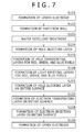
- FIG. 7 is a flow chart illustrating the method for production of the organic EL display device shown in FIG. 6 ;
- FIG. 8 is a schematic plan view depicting the module containing the display device according to the embodiment mentioned above;
- FIG. 9 is a perspective view depicting the appearance of the apparatus as the first example of application of the display device according to the embodiment mentioned above;
- FIG. 10A is a perspective view depicting the front appearance of the apparatus as the second example of application
- FIG. 10B is a perspective view depicting the rear appearance of the apparatus as the second example of application;
- FIG. 11 is a perspective view depicting the appearance of the apparatus as the third example of application.
- FIG. 12 is a perspective view depicting the appearance of the apparatus as the fourth example of application.
- FIGS. 13A to 13G are diagrams depicting the appearance of the apparatus as the fifth example of application, with FIG. 13A being a front view in the open state, FIG. 13B being a front view in the open state, FIG. 13C being a front view in the closed state, FIG. 13D being a left side view, FIG. 13E being a right side view, FIG. 13F being a top view, and FIG. 13G being a bottom view.
- First embodiment (covering the organic EL display device having the electron injecting/transporting layer formed on the light emitting layers for individual colors)
- Second embodiment (covering the organic EL display device having the hole blocking layer formed between the light emitting layers for individual colors and the electron injecting/transporting layer)
- the organic EL display device 1 is designed for use as the organic EL television set. It is composed of the substrate 11 and the display region 110 formed thereon.
- the display region 110 includes the red organic EL elements 10 R, the green organic EL elements 10 G, and the blue organic EL elements 10 B, which are arranged in a matrix pattern. A detailed description of these organic EL elements will be given later.
- the signal line drive circuit 120 and the scanning line drive circuit 130 are the signal line drive circuit 120 and the scanning line drive circuit 130 , both functioning as the driver for video display.
- the pixel drive circuits 140 are drive circuits of active type formed on the layer under the lower electrode 14 which will be mentioned later.
- Each of the pixel drive circuits 140 is composed of the drive transistor Tr 1 , the writing transistor Tr 2 , the capacitor (storage capacity) Cs placed between these transistors Tr 1 and Tr 2 , and the red organic EL element 10 R (or the green organic EL element 10 G or the blue organic EL element 10 B) which is placed between the first source line (Vcc) and the second source line (GND) and is serially connected to the drive transistor Tr 1 .
- the drive transistor Tr 1 and the writing transistor Tr 2 are ordinary thin film transistors (TFT). These transistors may be arranged unrestrictedly in the inverted stagger type (bottom gate type) or in the stagger type (top gate type).
- the pixel drive circuit 140 has the signal lines 120 A arranged in the column direction and the scanning lines 130 A arranged in the row direction. Each of the signal lines 120 A and each of the scanning lines 130 A cross each other at the intersection which corresponds to one of the red organic EL element 10 R, the green organic EL element 10 G, or the blue organic EL element 10 B, which serves as a subpixel. Each of the signal lines 120 A is connected to the signal line drive circuit 120 , so that the signal line drive circuit 120 supplies image signals to the source electrode of the writing transistor Tr 2 through the signal line 120 A. Likewise, each of the scanning lines 130 A is connected to the scanning line drive circuit 130 , so that the scanning line drive circuit 130 supplies scanning signals to the gate electrode of the writing transistor Tr 2 through the scanning line 130 A.
- the display region 110 also has the red organic EL element 10 R for red color emission, the green organic EL element 10 G for green color emission, and the blue organic EL element 10 B for blue color emission, which are arranged side by side in a matrix pattern.
- One combination of these adjoining three elements constitutes one pixel.
- the display region 110 is constructed as shown in FIG. 3 which is a sectional view.
- Each of the red organic EL element 10 R, the green organic EL element 10 G, and the blue organic EL element 10 B is composed of the substrate 11 , the drive transistor Tr 1 of the pixel drive circuit 140 (not shown), the planarized insulating film (not shown), the lower electrode 14 as the anode, the partition wall 15 , the organic layer 16 , and the upper electrode 17 as the cathode, which are sequentially arranged upward.
- the organic layer 16 includes light emitting layers 16 C (the red emitting layer 16 CR, the green emitting layer 16 CG, and the blue emitting layer 16 CB), which will be described later.
- the red organic EL element 10 R, the green organic EL element 10 G, and the blue organic EL element 10 B are covered with the protective layer 30 .
- the protective layer 30 is entirely covered with the sealing substrate 40 , with a bonding layer (not shown) interposed between them.
- the bonding layer is formed from a thermosetting resin or a UV (ultra violet) curable resin. In this way the entire assembly is completely sealed.
- the substrate 11 is a support on one surface of which are arranged and formed the red organic EL element 10 R, the green organic EL element 10 G, and the blue organic EL element 10 B. It may be any known one made of quartz, glass, metal foil, or plastics in the form of film or sheet. A substrate of quarts or glass is preferable. Adequate materials for plastic substrates include methacrylic resin, such as polymethyl methacrylate (PMMA), polyesters, such as polyethylene terephthalate (PET), polyethylene naphthalate (PEN), and polybutylene naphthalate (PBN), and polycarbonate resin. These plastics need surface coating or surface treatment to eliminate their water and gas permeability.
- PMMA polymethyl methacrylate
- PET polyethylene terephthalate
- PEN polyethylene naphthalate
- PBN polybutylene naphthalate
- the lower electrode 14 is formed on the substrate 11 for each of the red organic EL element 10 R, the green organic EL element 10 G, and the blue organic EL element 10 B.
- the lower electrode 14 has a thickness of 10 nm to 1,000 nm (measured in the direction of layer arrangement). It is formed from any one of such metals (or alloys thereof) as chromium (Cr), gold (Au), platinum (Pt), nickel (Ni), copper (Cu), tungsten (W), and silver (Ag).
- the lower electrode 14 may have a laminate structure composed of a film of the metal or alloy and a transparent conductive film of indium-tin oxide (ITO), indium-zinc oxide (InZnO), or alloy of zinc oxide (ZnO) and aluminum.
- ITO indium-tin oxide
- InZnO indium-zinc oxide
- ZnO zinc oxide
- aluminum aluminum
- the lower electrode 14 should preferably be formed from a material highly capable of hole injection.
- it may also be formed from any material such as aluminum alloy which has a surface oxide film or which poses a problem with hole injection barrier due to its small work function, so long as the hole injecting layers 16 A are adequately provided.
- the partition wall 15 ensures insulation between the lower electrode 14 and the upper electrode 17 , and it also demarcates the emission region in a desired shape. In addition, the partition wall 15 also functions as a separator for individual layers at the time of ink jet coating or nozzle coating in the fabricating process mentioned later.
- the partition wall 15 is composed of the lower partition wall 15 A and the upper partition wall 15 B, the former being made of inorganic insulating material such as SiO 2 and the latter being made of photosensitive resin such as polybenzoxazole or polyimide (both being of positive photosensitive type).
- the partition wall 15 has an opening corresponding to the emission region.
- the organic layer 16 and the upper electrode 17 may be formed not only on the opening but also on the partition wall 15 ; however, it is only the opening of the partition wall 15 that produces emission.
- the organic layer 16 of the red organic EL element 10 R is composed of the hole injecting layer 16 AR, the hole transporting layer 16 BR, the red emitting layer 16 CR, the electron transporting layer 16 D, and the electron injecting layer 16 E, which are sequentially arranged upward from the lower electrode 14 .
- the organic layer 16 of the green organic EL element 10 G is composed of the hole injecting layer 16 AG, the hole transporting layer 16 BG, the green emitting layer 16 CG, the electron transporting layer 16 D, and the electron injecting layer 16 E, which are sequentially arranged upward from the lower electrode 14 .
- the organic layer 16 of the blue organic EL element 10 B is composed of the hole injecting layer 16 AB, the hole transporting layer 16 BB, the blue emitting layer 16 CB, the electron transporting layer 16 D, and the electron injecting layer 16 E, which are sequentially arranged upward from the lower electrode 14 .
- the electron transporting layer 16 D and the electron injecting layer 16 E of the foregoing layers is formed as a common layer for the red organic EL element 10 R, the green organic EL element 10 G, and the blue organic EL element 10 B.
- the hole injecting layers 16 AR, 16 AG, and 16 AB are intended to improve the efficiency of hole injection into the emitting layers 16 CR, 16 CG, and 16 CB. They function also as a buffer layer to prevent leakage. They are provided on the lower electrode 14 for the red organic EL element 10 R, the green organic EL element 10 G, and the blue organic EL element 10 B individually.
- the hole injecting layers 16 AR, 16 AG, and 16 AB should preferably have a thickness of 5 nm to 10 nm, more preferably 8 nm to 50 nm. They may be formed from any material compatible with their adjoining electrodes and layers. Typical examples of such materials include polyaniline, polythiophene, polypyrrole, polyphenylenevinylene, polythienylenevinylene, polyquinoline, and polyquinoxaline, and derivatives thereof; conductive polymers such as those having the aromatic amine structure in the main chain or side chain; and metal phthalocyanine (such as copper phthalocyanine) and carbon.
- the polymeric material used for the hole injecting layers 16 AR, 16 AG, and 16 AB should have a weight-average molecular weight (Mw) of 10,000 to 300,000, preferably 50,000 to 200,000.
- Mw weight-average molecular weight
- the polymeric material may be replaced by an oligomer having a molecular weight of 2,000 to 10,000. If the hole injecting layer is formed from a polymeric material having a molecular weight lower than 50,000, it will dissolve when the hole transporting layer and its ensuing layers are formed. On the other hand, any polymeric material having a molecular weight higher than 300,000 will undergo gelling, which presents difficulties in film formation.
- the conductive polymeric material used for the hole injecting layers 16 AR, 16 AG, and 16 AB typically includes polyaniline, oligoaniline, and polydioxythiophene such as poly(3,4-ethylenedioxythiophene) (PEDOT). Additional examples include Nafion (trademark) and Liquion (trademark) (in solution form) from H.C. Starck Inc., EL-Source (trademark) from Nissan Chemical Industries, Ltd., and Berazol (trademark) which is a conductive polymer from Soken Chemical & Engineering Co., Ltd.
- the red organic EL element 10 R, the green organic EL element 10 G, and the blue organic EL element 10 B adjoin respectively to the hole transporting layers 16 BR, 16 BG, and 16 BB, which improve the efficiency of hole transportation to the red emitting layer 16 CR, the green emitting layer 16 CG, and the blue emitting layer 16 CB.
- the hole transporting layers 16 BR, 16 BG, and 16 BB are formed respectively on the hole injecting layers 16 AR, 16 AG, and 16 AB for the red organic EL element 10 R, the green organic EL element 10 G, and the blue organic EL element 10 B.
- the hole transporting layers 16 BR, 16 BG, and 16 BB should have a thickness ranging from 10 nm to 200 nm, preferably from 15 nm to 150 nm, depending on the entire structure of the element. They may be formed from a variety of solvent-soluble light-emitting polymeric materials, such as polyvinylcarbazole, polyfluorene, polyaniline, and polysilane, and derivatives thereof; polysiloxane derivatives having an aromatic amine in the main chain or side chain; polythiophene and derivatives thereof; and polypyrrole.
- solvent-soluble light-emitting polymeric materials such as polyvinylcarbazole, polyfluorene, polyaniline, and polysilane, and derivatives thereof; polysiloxane derivatives having an aromatic amine in the main chain or side chain; polythiophene and derivatives thereof; and polypyrrole.
- Other preferable polymeric materials are those which are represented by the formula (1) below and soluble in organic solvents. They provide the hole transporting layers 16 BR, 16 BG, and 16 BB with good adhesion to the hole injecting layers 16 AR, 16 AG, and 16 AB and the light emitting layers 16 CR, 16 CG, and 16 CB placed thereunder and thereon, respectively.
- A13 to A16 each denotes a group having 1 to 10 aromatic hydrocarbon groups or a derivative thereof, or a group having 1 to 15 heterocyclic groups or a derivative thereof; n and m each denotes an integer of 0 to 10,000, with n+m being an integer of 10 to 20,000.
- the polymeric material may be any of random polymer, alternating copolymer, periodic copolymer, or block copolymer, with the moieties denoted by n and m being arranged in any order.
- the values of n and m should preferably be an integer of 5 to 5,000, more preferably 10 to 3,000, with their sum (n+m) being an integer of 10 to 10,000, more preferably 20 to 6,000.
- the aromatic hydrocarbon groups represented by A13 to A16 are exemplified by benzene, fluorene, naphthalene, and anthracene, and derivatives thereof; phenylenevinylene derivatives; and styryl derivatives.
- the heterocyclic groups are exemplified by thiophene, pyridine, pyrrole, and carbazole, and derivatives thereof.
- the groups A13 to A16 in the compound represented by the formula (1) above may have substituent groups.
- substituent groups should be C 1-12 straight or branched alkyl groups or alkenyl groups, whose typical examples include methyl group, ethyl group, propyl group, isopropyl group, butyl group, isobutyl group, sec-butyl group, tert-butyl group, pentyl group, hexyl group, heptyl group, octyl group, nonyl group decyl group, undecyl group, dodecyl group, vinyl group, and allyl group.
- Typical but nonrestrictive examples of the compound represented by the formula (1) above include those compounds represented by the formulas (1-1) to (1-3) below. Their chemical names are listed below.
- Formula (1-1) poly[(9,9-dioctylfluorenyl-2,7-diyl)-co-(4,4′-(N-(4-sec-butylphenyl))diphenylamine)] (TFB)
- the red, green, and blue emitting layers 16 CR, 16 CG, and 16 CB are the sites where electrons and holes undergo recombination in the presence of electric field, thereby emitting light.
- Each of them should have a thickness ranging from 10 nm to 200 nm, preferably 15 nm to 150 nm, depending on the entire structure of the element. They are formed from a light-emitting polymeric material incorporated with a low-molecular weight material, which should preferably be a monomer or an oligomer composed of 2 to 10 monomers and have a weight-average molecular weight not higher than 10,000. (This molecular weight is not an index for discrimination of materials.)
- the red, green, and blue emitting layers 16 CR, 16 CG, and 16 CB may be formed by coating method, such as ink jet technology which will be detailed later. This coating is accomplished by using a solution of the polymeric material and the low-molecular weight material dissolved in at least one organic solvents, such as toluene, xylene, anisole, cyclohexanone, mesitylene (1,3,5-trimethylbenzene), pseudocumene (1,2,4-trimethylbeznene), dihydrobenzofuran, 1,2,3,4-tetramethylbenzene, tetralin, cyclohexylbenzene, 1-methylnaphthalene, p-anisyl alcohol, dimethylnaphthalene, 3-methylbiphenyl, 4-methylbiphenyl, 3-isopropylbiphenyl, and monoisopropylnaphthalene.
- organic solvents such as toluene, xylene, anisole
- the polymeric materials (for light emission) constituting the red, green, and blue emitting layers 16 CR, 16 CG, and 16 CB include, for example, polyfluorene derivatives, polyphenylenevinylene derivatives, polyphenylene derivatives, polyvinylcarbazole derivatives, and polythiophene derivatives, which are capable of light emission.
- the red emitting layer 16 CR is formed from ADS111RE (trademark) represented by the formula (2-1) below
- the green emitting layer 16 CG is formed from ADS109GE (trademark) represented by the formula (2-2) below
- the blue emitting layer 16 CB is formed from ADS136BE (trademark) represented by the formula (2-3) below, all of these products being available from American Dye Source Inc.
- These emitting layers rely on singlet excitons for light emission.
- the polymeric material used in this embodiment includes not only conjugated polymers but also non-conjugated polymer of pendant type or non-conjugated polymer mixed with a dye.
- the red, green, and blue emitting layers 16 CR, 16 CG, and 16 CB may emit light from single excitons or triplet excitons or both.
- light-emitting materials include aromatic hydrocarbon compounds and heterocyclic compounds exemplified below.
- Additional examples include those compounds involving the triplet excited state which contain iridium metal complex or the like.
- the foregoing examples are not limitative ones.
- the light-emitting polymeric material capable of light emission in the triplet excited state include, for example, RPP, GPP, and BPP represented respectively by the formulas (3-1), (3-2), and (3-3) below. These compounds emit red, green, and blue light by phosphorescence, respectively.
- the polymeric material that constitutes the red, green, and blue emitting layers 16 CR, 16 CG, and 16 CB should preferably be incorporated with a low-molecular weight material, which improves the efficiency of hole and electron injection into the red, green, and blue emitting layers 16 CR, 16 CG, and 16 CB from the electron transporting layer 16 D. This is based on the principle explained below.
- red, green, and blue emitting layers 16 CR, 16 CG, and 16 CB are formed only from polymeric materials suitable for them and they are coated with the electron transporting layer 16 D formed from a low-molecular weight material, there will be a large difference in energy level between the red, green, and blue emitting layers 16 CR, 16 CG, and 16 CB and the electron transporting layer 16 D. This leads to an extremely low efficiency in hole or electron injection from the electron transporting layer 16 D into the red, green, and blue emitting layers 16 CR, 16 CG, and 16 CB, with the result that the emitting layers formed from the polymeric materials do not exhibit their inherent characteristic properties.
- red, green, and blue emitting layers 16 CR, 16 CG, and 16 CB with a low-molecular weight material (monomer or oligomer) which reduces the difference in energy level between the red, green, and blue emitting layers 16 CR, 16 CG, and 16 CB and the electron transporting layer 16 D.
- a low-molecular weight material monomer or oligomer
- the low-molecular weight material is selected from those compounds which have a value deeper than the LUMO of the red emitting layer 16 CR or the green emitting layer 16 CG and also have a value shallower than the LUMO of the electron transporting layer 16 D and which further have a value deeper than the HOMO of the red emitting layer 16 CR, the green emitting layer 16 CG, and the blue emitting layer 16 CB and also have a value shallower than the HOMO of the electron transporting layer 16 D.
- the materials to be used for the red, green, and blue emitting layers 16 CR, 16 CG, and 16 CB are not necessarily restricted by the values of HOMO and LUMO mentioned above. This holds true in the case where the hole blocking layer 26 F (mentioned later) is placed between the red, green, and blue emitting layers 26 CR, 26 CG, and 26 CB and the electron transporting layer 26 D.
- the hole blocking layer 26 F capable of electron transportation may have a LUMO which is shallower than that of the low-molecular weight material for the red, green, and blue emitting layers 26 CR, 26 CG, and 26 CB.
- the low-molecular weight material to be incorporated into the light emitting layers 26 C is not restricted to one kind; materials differing in energy level may be used in combination in order to ensure smooth hole or electron transportation.
- the low-molecular weight material to be incorporated into the red, green, and blue emitting layers 16 CR, 16 CG, and 16 CB denotes any compound having substantially a single value of molecular weight but excludes any polymers and condensates having a high molecular weight which result from low-molecular weight compounds by continuous repetition of identical or similar reactions.
- such low-molecular weight materials remain in the form of substantially separate molecules (free of intermolecular linking) even when they are heated.
- Such low-molecular weight materials should preferably have a weight-average molecular weight (Mw) not higher than 10,000, such that the ratio of molecular weight is not lower than 10 between the polymeric material and the low-molecular weight material.
- the material having a molecular weight lower than 10,000 is more desirable than the material having a higher molecular weight, for example 50,000, because the former has varied characteristic properties and is easily adjustable for the mobility of holes or electrons, the band gap, and the solubility in solvents.
- the low-molecular weight material should be added in such an amount that the mixing ratio of the polymeric material for the red, green, and blue emitting layers 16 CR, 16 CG, and 16 CB and the low-molecular weight material is from 20:1 to 1:1 by weight. With a mixing ratio lower than 20:1, the low-molecular weight material does not fully produce its effect. With a mixing ratio higher than 1:1, the polymeric material does not produce its effect as the light-emitting material.
- the incorporation of a low-molecular weight material into the red, green, and blue emitting layers 16 CR, 16 CG, and 16 CB permits easy adjustment of the carrier balance for holes and electrons. Without this effect, electron injection (into the red, green, and blue emitting layers 16 CR, 16 CG, and 16 CB) and hole transportation will be deteriorated as the result of formation of the electron transporting layer 16 D which will be mentioned later.
- the foregoing contributes to high emitting efficiency and extended life and reduced drive voltage of the red, green, and blue organic EL elements 10 R, 10 G, and 10 B.
- the low-molecular weight compound includes, for example, benzidine, styrylamine, triphenylamine, porphyrin, triphenylene, azatriphenylene, teteracyanoquinodimethane, triazole, imidazole, oxadiazole, polyarylalkane, phenylenediamine, arylamine, oxazole, anthracene, fluorenone, hydrazone, and stilbene, and derivatives thereof.
- Additional examples include heterocyclic conjugate monomer or oligomer such as polysilane compounds, vinylcarbazole compounds, thiophene compounds, and aniline compounds.
- low-molecular weight materials are those represented by the formulas (4) to (6) below.
- A1 to A3 denote aromatic hydrocarbon groups, heterocyclic groups, or derivatives thereof.
- Z denotes a nitrogen-containing hydrocarbon group or a derivative thereof
- L1 denotes a divalent group formed from one to four aromatic rings joined together or a derivative thereof
- A4 and A5 each denotes an aromatic hydrocarbon group or an aromatic heterocyclic group or a derivative thereof, provided that A4 and A5 may form a cyclic structure as they join together.
- L2 denotes a divalent group formed from two to six aromatic rings joined together, or a derivative thereof; and A6 to A9 each denotes an aromatic hydrocarbon group or a heterocyclic group or a group formed from one to ten derivatives thereof joined together.
- the compounds represented by the formula (5) are exemplified by those represented by the formulas (5-1) to (5-166) below.
- the nitrogen-containing hydrocarbon group linking to L1 may be a carbazole group, indole group, or imidazole group.
- the low-molecular weight compound to be incorporated into the red, green, and blue emitting layers 16 CR, 16 CG, and 16 CB includes those represented by the formula (7) without restrictions.
- R24 to R29 each denotes a hydrogen atom, halogen atom, hydroxyl group, alkyl group with a carbon number of 20 or less, alkenyl group, a group having a carbonyl group, a group having a carbonylester group, a group having an alkoxyl group, a group having a cyano group, a group having a nitro group, a derivative thereof, a group having a silyl group with a carbon number of 30 or less, a group having an aryl group, a group having a heterocyclic group, or a group having an amino group, or a derivative thereof.
- the compound represented by the formula (7) has the groups R24 to R29, each having an aryl group, as mentioned above. They are exemplified by phenyl group, 1-naphthyl group, 2-naphthyl group, fluorenyl group, 1-anthryl group, 2-anthryl group, 9-anthryl group, 1-phenanthryl group, 2-phenanthryl group, 3-phenanthryl group, 4-phenanthryl group, 9-phenanthryl group, 1-naphthacenyl group, 2-naphthacenyl group, 9-naphthacenyl group, 1-pyrenyl group, 2-pyrenyl group, 4-pyrenyl group, 1-chrysenyl group, 6-chrysenyl group, 2-fluoranthenyl group, 3-fluoranthenyl group, 2-biphenylyl group, 3-biphenylyl group, 4-biphenylyl group, o-tolyl group,
- the compound represented by the formula (7) has the groups R24 to R29, each having a heterocyclic group, as mentioned above.
- the heterocyclic group is a five- or six-membered aromatic ring including oxygen (O), nitrogen (N), or sulfur (S) as the hetero atom. It is a C 2-20 condensed polycyclic aromatic group exemplified below. Thienyl group, furyl group, pyrrolyl group, pyridyl group, quinolyl group, quinoxalyl group, imidazopyridyl group, and benzothiazole group.
- the groups R24 to R29 each having an amino group, include alkylamino groups, arylamino groups, and aralkylamino groups. These groups should preferably have C 1-6 aliphatic hydrocarbon groups and/or C 1-4 aromatic cyclic groups, such as dimethylamino group, diethylamino group, dibutylamino group, diphenylamino group, ditolylamino group, bisbiphenylylamino group, and dinaphthylamino group.
- the above-mentioned substituent group may form a condensed ring composed of two or more substituent groups, or may include its derivatives.
- the compound represented by the formula (7) is typically exemplified by those represented by the formulas (7-1) to (7-51).
- the low-molecular weight compound to be incorporated into the red, green, and blue emitting layers 16 CR, 16 CG, and 16 CB includes those capable of electron transportation.
- Their typical but nonrestrictive examples are benzoimidazole derivatives, pyridylphenyl derivatives, and bipyridine derivatives, which are represented by the following formulas (8), (9), and (10), respectively.
- A10 denotes hydrogen atom, a halogen atom, C 1-20 alkyl group, C 6-60 hydrocarbon group having a polycyclic aromatic hydrocarbon group formed by condensation from 3 to 40 aromatic rings, or nitrogen-containing heterocyclic group, or a derivative thereof
- B denotes a single bond, or a divalent aromatic cyclic group or a derivative thereof
- R7 and R8 each independently denotes a hydrogen atom, halogen atom, C 1-20 alkyl group, C 6-60 aromatic hydrocarbon group, nitrogen-containing heterocyclic group, or C 1-20 alkoxyl group, or a derivative thereof.
- A11 denotes a n-valent group formed by condensation from two to five aromatic rings (typically n-valent acene aromatic ring formed by condensation from three aromatic rings) or a derivative thereof;
- R9 to R14 each independently denotes a hydrogen atom, halogen atom, or a free valance linking to any one of A11 or R15 to R19;
- R15 to R19 each independently denotes a hydrogen atom, halogen atom, or a free valance linking to any one of R9 to R14;
- n is an integer of 2 or above.
- the pyridylphenyl groups existing as many as n may be identical or different.
- A12 denotes an m-valent group formed by condensation from two to five aromatic rings (typically m-valent acene aromatic ring formed by condensation from three aromatic rings) or a derivative thereof;
- R20 to R24 each independently denotes a hydrogen atom, halogen atom, or a free valance linking to any one of A12 or R25 to R29;
- R25 to R29 each independently denotes a hydrogen atom, halogen atom, or a free valance linking to any one of R20 to R24;
- m is an integer of 2 or above.
- the bipyridyl groups existing as many as m may be identical or different.
- the compounds represented by the formula (8) are typically exemplified by those represented by the formulas (8-1) to (8-49) below.
- Ar( ⁇ ) corresponds to the benzoimidazole skeleton containing R7 and R8 shown in the formula (8) and B corresponds to B shown in the formula (8).
- Ar(1) and Ar(2) correspond to A10 shown in the formula (8), and they are bonded to B sequentially in the order of Ar(1) and Ar(2).
- the compounds represented by the formula (9) are typically exemplified by those represented by the formulas (9-1) to (9-81) below.
- the compounds represented by the formula (10) are typically exemplified by those represented by the formulas (10-1) to (10-17) below.
- the low-molecular weight compound to be incorporated into the red, green, and blue emitting layers 16 CR, 16 CG, and 16 CB includes pyrazole derivatives represented by the formula (11) below, in addition to those compounds represented by the formulas (8) to (10) above.
- R30 to R32 each denotes a hydrogen atom, an aromatic hydrocarbon group formed by condensation from one to three aromatic rings or a derivative thereof, an aromatic hydrocarbon group formed by condensation from one to three aromatic rings each having C 1-6 hydrocarbon groups or a derivative thereof, or an aromatic hydrocarbon group formed by condensation from one to three aromatic rings each having C 6-12 aromatic hydrocarbon groups or a derivative thereof.
- the aromatic hydrocarbon groups represented by R30 to R32 include unrestrictedly phenyl group, 2-methylphenyl group, 3-methylphenyl group, 4-methylphenyl group, 2,4-dimethylphenyl group, 3,4-dimethylphenyl group, 2,4,5-trimethylphenyl group, 4-ethylphenyl group, 4-tert-butylphenyl group, 1-naphthyl group, 2-naphthyl group, 1-anthracenyl group, 2-anthracenyl group, 9-anthracenyl group, and 9-phenanthrenyl group.
- R30 to R32 may be identical or different.
- the compound represented by the formula (11) is typically exemplified by those represented by the formulas (11-1) to (11-5) below which have two or three pyrazole structures in the same molecule.
- the low-molecular weight compound may be replaced by any phosphorescent material, such as metal complex containing at least one metal element selected from beryllium (Be), boron (B), zinc (Zn), cadmium (Cd), magnesium (Mg), gold (Au), silver (Ag), palladium (Pd), platinum (Pt), aluminum (Al), gadolinium (Ga), yttrium (Y), scandium (Sc), ruthenium (Ru), rhodium (Rh), osmium (Os), and iridium (Ir).
- metal complexes containing at least one metal element selected from beryllium (Be), boron (B), zinc (Zn), cadmium (Cd), magnesium (Mg), gold (Au), silver (Ag), palladium (Pd), platinum (Pt), aluminum (Al), gadolinium (Ga), yttrium (Y), scandium (Sc), ruthenium (Ru), rhodium (
- the low-molecular weight material to be incorporated into the red, green, and blue emitting layers 16 CR, 16 CG, and 16 CB is not limited to one species. More than one species may be used in combination.
- the electron transporting layer 16 D is intended to improve the efficiency of electron transportation into the red, green, and blue emitting layers 16 CR, 16 CG, and 16 CB, and it is formed as a common layer over the entire surface of these layers.
- the thickness of the electron transporting layer 16 D ranges from 5 nm to 300 nm, preferably from 10 nm to 170 nm, depending on the entire structure of the element.
- the electron transporting layer 16 D should preferably be formed from an organic material highly capable of electron transportation.
- the improved efficiency of electron transportation into the light emitting layer 16 C prevents the red, green, and blue organic EL elements 10 R, 10 G, and 10 B from fluctuating in emission color due to the intensity of electric field which will be mentioned later.
- An example of the organic material is a nitrogen-containing heterocyclic derivative having an electron mobility no lower than 10 ⁇ 6 cm 2 /Vs and no higher than 1.0 ⁇ 10 ⁇ 1 cm 2 /Vs.
- the organic material for the electron transporting layer 16 D is not limited to one species. More than one species may be used together in combination or separately in laminate form. In addition, it may also be incorporated into the electron injecting layer 16 E which will be mentioned later.
- the electron injecting layer 16 E is intended to improve the efficiency of electron injection, and it is formed as a common layer over the entire surface of the electron transporting layer 16 D.
- the electron injecting layer 16 E may be formed from lithium oxide (LiO 2 ) or cesium carbonate (Cs 2 CO 3 ) or a mixture thereof. Additional examples include alkaline earth metals, such as calcium (Ca) and barium (Ba), and alkali metals, such as lithium (Li) and cesium (Ce), and such metal as indium (In) and magnesium (Mg) having a small work function. These metals may be used alone or in combination in the form alloy, oxide, complex oxide, or fluoride for better stability. It is also possible to use the above-mentioned organic compounds represented by the formulas (8-1) to (11-5) as the material for the electron transporting layer 16 D.
- the upper electrode 17 is a conductive metal film having a thickness of 2 nm to 15 nm.
- the conductive metal is Al, Mg, Ca, or Na in alloy form.
- An alloy of magnesium and silver (Mg—Ag alloy) is desirable on account of its good conductivity and its low light absorption in its thin film form.
- the Mg—Ag alloy is not specifically restricted in the ratio of magnesium to silver.
- a desirable Mg/Ag ratio is from 20/1 to 1/1 in terms of film thickness.
- the upper electrode 17 may also be formed from an alloy of Al and Li (Al—Li alloy).
- the upper electrode 17 may be a layer formed from a mixture containing such organic emitting materials as aluminum-quinoline complex, styrylamine derivative, and phthalocyanine derivative.
- the upper electrode 17 may have an additional layer of MgAg capable of light transmission.
- the upper electrode 17 is formed (in the form of film) over the entire surface of the substrate 11 in such a way that it is insulated from the lower electrode 14 by the organic layer 16 and the partition wall 15 , and it functions as a common electrode for the red, green, and blue organic EL elements 10 R, 10 G, and 10 B.
- the protective film 30 which is for example 2 to 3 ⁇ m in thickness, may be formed from either insulating material or conductive material.
- the insulating material may be an inorganic one in amorphous form, such as amorphous silicon (a-Si), amorphous silicon carbide (a-SiC), amorphous silicon nitride (a-Si 1-x N x ), and amorphous carbon (a-C).
- amorphous silicon a-Si
- a-SiC amorphous silicon carbide
- a-Si 1-x N x amorphous silicon nitride
- a-C amorphous carbon
- the sealing substrate 40 is placed over the upper electrode 17 for the red, green, and blue organic EL elements 10 R, 10 G, and 10 B. It, in conjunction with the adhesion layer (not shown), seals the red, green, and blue organic EL elements 10 R, 10 G, and 10 B.
- the sealing substrate 40 is formed from a material such as glass transparent to light generated by the red, green, and blue organic EL elements 10 R, 10 G, and 10 B.
- the sealing substrate 40 is provided with a color filter and a shielding film as a black matrix (both not shown), which permit the light generated by the red, green, and blue organic EL elements 10 R, 10 G, and 10 B to go out and also absorb external light reflected by the red, green, and blue organic EL elements 10 R, 10 G, and 10 B and wiring arranged thereunder, thereby improving contrast.
- a color filter and a shielding film as a black matrix (both not shown)
- the sealing substrate 40 has nothing to do with transmittance of visible light.
- the color filter is composed of red, green, and blue filters (all not shown) which are arranged over the red, green, and blue organic EL elements 10 R, 10 G, and 10 B, respectively.
- the red, green, and blue filters are tightly arranged side by side in rectangular form. They are formed from plastic resin incorporated with pigment. Selection of an adequate pigment makes it possible to increase or decrease the transmittance of desired light having a wavelength within or without the range of red, green, and blue.
- the color filter has a high transmittance for light with a certain wavelength which coincides with the peak wavelength ⁇ of the spectrum of light emerging from the resonating structure. As the result, the color filter transmits only a fraction of external light incident to the sealing substrate 40 which has the same wavelength as the peak wavelength ⁇ of the spectrum of desired light but prevents the remainder of external light from entering the organic EL elements 10 R, 10 G, and 10 B.
- the shielding film is a black resin film having an optical density not lower than 1 which is incorporated with a black colorant, or a thin-film filter that produces thin film interference.
- the black resin film is economically desirable.
- the thin-film filter is a laminate composed of thin films of metal, metal nitride, or metal oxide. It is intended to attenuate light by means of interference produced by thin films.
- a typical example is a laminate composed of thin films of chromium (Cr) and chromium (iii) oxide (Cr 2 O 3 ) placed one over another.
- the organic EL display device 1 mentioned above may be produced in the following way.
- the organic EL display device is produced according to the flow chart shown in FIG. 4 . Individual steps of the production process are sequentially shown in FIGS. 5A to 5G .
- the first step starts with preparing the substrate 11 from the above-mentioned material, forming thereon the pixel drive circuit 140 including the drive transistor Tr 1 , and forming a planarized insulating film of photosensitive resin (not shown).
- Step S 101 the substrate 11 is entirely coated with a transparent conductive film of ITO, which is subsequently patterned to form the lower electrodes 14 individually for the red, green, and blue EL elements 10 R, 10 G, and 10 B, as shown in FIG. 5A .
- each of the lower electrodes 14 is made to communicate with the drain electrode of the drive transistor Tr 1 through a contact hole (not shown) formed in the planarized insulating film (not shown).
- Step S 102 the planarized insulating film (not shown) and the lower electrodes 14 are coated with an inorganic insulating material such as SiO 2 by CVD (chemical vapor deposition), and the resulting film is patterned by photolithography and etching, so that the lower partition walls 15 A are formed, as shown in FIG. 5A .
- CVD chemical vapor deposition
- the lower partition walls 15 A are overlaid with the upper partition walls 15 B made of the above-mentioned photosensitive material, as shown in FIG. 5A .
- the upper partition walls 15 B are so formed as to surround the emitting region of the pixel. In this way there are obtained the partition walls 15 each composed of the upper partition wall 15 B and the lower partition wall 15 A in step S 102 .
- the substrate 11 on which the lower electrodes 14 and the partition walls 15 have been formed undergoes oxygen-plasma treatment, so that the surface of the substrate is cleaned of contaminants (organic matter) for improvement in wettability.
- the substrate 11 is heated at about 70 to 80° C. and oxygen plasma treatment is conducted under atmospheric pressure.
- Step S 103 the plasma treatment is followed by the water repellent treatment, so that the top and side of the upper partition 15 B wall decreases in wettability.
- plasma treatment with tetrafluoromethane (CF 4 ) is conducted under atmospheric pressure, followed by cooling to room temperature. In this way the top and side of the upper partition wall 15 B is made less wettable.
- the exposed part of the lower electrode 14 and the lower partition wall 15 A are slightly affected by the CF 4 plasma treatment, they retain the improved wettability achieved by the oxygen plasma treatment because their constituent materials (ITO and SiO 2 ) are incompatible with fluorine.
- Step 104 which follows the water repellent treatment, the hole injecting layers 16 AR, 16 AG, and 16 AB are formed as shown in FIG. 5B , each in the region surrounded by the upper partition wall 15 B, from the above-mentioned materials by spin coating, drop delivery coating method or the like.
- ink jet coating or nozzle coating as drop delivery coating method is desirable for precise allocation of materials.
- hole injecting layers 16 AR, 16 AG, and 16 AB a solution or dispersion of polyaniline, polythiophene, or the like is applied to the exposed part of the lower electrode 14 by ink jet coating, which is followed by heating for drying.
- the drying step is further followed by heating at a higher temperature in oxygen or in the atmosphere, so that the conductive polymeric material such as polyaniline and polythiophene becomes more conductive due to oxidization.
- Heating in this step should be carried out at 150 to 300° C., preferably 180 to 250° C., for 5 to 300 minutes, preferably 10 to 240 minutes depending on the heating temperature and atmosphere, so that the dried film has a thickness of 5 nm to 100 nm, preferably 8 nm to 50 nm.
- Step S 105 shown in FIG. 5C the hole transporting layers 16 BR, 16 BG, and 16 BB, each containing the above-mentioned polymeric material, are formed by spin coating method and drop delivery coating method respectively on the hole injecting layers 16 AR, 16 AG, and 16 AB, which have been formed in Step S 104 .
- Ink jet coating or nozzle coating as delivery coating method is desirable for precise allocation of materials to the region surrounded by the upper partition walls 15 B.
- hole transporting layers 16 BR, 16 BG, and 16 BB a mixed solution or dispersion of the polymeric material and low-molecular weight material is applied respectively to the exposed surfaces of the hole injecting layers 16 AR, 16 AG, and 16 AB by, for example, ink jet coating, which is followed by heating for drying. In this way there are formed the hole transporting layers 16 BR, 16 BG, and 16 BB for the red, green, and blue organic EL elements 10 R, 10 G, and 10 B.
- the drying step is further followed by heating at a higher temperature. Drying and subsequent heating should be carried out preferably in an atmosphere composed mainly of nitrogen (N 2 ) substantially free of oxygen and water vapor which are detrimental to the emission efficiency and life of the resulting organic EL display device.
- the effect of oxygen and water vapor is significant in the heating step.
- the oxygen concentration should be 0.1 to 100 ppm, preferably not higher than 50 ppm. With an oxygen concentration higher than 100 ppm, the resulting organic EL display device will be poor in emission efficiency and life due to contamination on the interface between thin films formed. However, processing with an oxygen concentration lower than 0.1 ppm is impracticable from the standpoint of equipment cost.
- the concentration of water vapor expressed in terms of dew point should be ⁇ 80° C. to ⁇ 40° C., preferably not higher than ⁇ 50° C., more preferably not higher than ⁇ 60° C.
- Water vapor with a dew point higher than ⁇ 40° C. causes contamination to the interface between thin films formed, thereby deteriorating the emission efficiency and life of the resulting organic EL display device. Keeping the concentration of water vapor below a dew point of ⁇ 80° C. is impracticable in mass production at this point from the standpoint of equipment cost.
- the heating temperature in this step should be 100 to 230° C., preferably 100 to 200° C. It should be lower than that in the step of forming the hole injecting layers 16 AR, 16 AG, and 16 AB.
- the duration of heating should be 5 to 300 minutes, preferably 10 to 240 minutes, depending on the heating temperature and atmosphere.
- the dried film should have a thickness of 10 nm to 200 nm, preferably 15 nm to 150 nm, depending on the entire structure of the element.
- the red, green, and blue emitting layers 16 CR, 16 CG, and 16 CB are formed from a mixture of the above-mentioned polymeric material and low-molecular weight material respectively on the hole transporting layers 16 BR, 16 BG, and 16 BB for the red, green, and blue organic EL elements 10 R, 10 G, and 10 B.
- This step is carried out by spin coating or drop delivery coating. Specifically, it is desirable to conduct ink jet coating or nozzle coating as drop delivery coating for precise allocation of materials to the regions surrounded by the upper partition walls 15 B.
- a mixed solution or dispersion of the polymeric material and low-molecular weight material is applied respectively to the exposed surfaces of the hole transporting layers 16 BR, 16 BG, and 16 BB by ink jet coating, for example.
- the solution or dispersion contains 1 wt % of solute in a 2:8 mixture of xylene and cyclohexylbenzene.
- This coating step is followed by heat treatment (for drying) in the same way as in the step of forming the hole transporting layers 16 BR, 16 BG, and 16 BB for the red, green, and blue organic EL elements 10 R, 10 G, and 10 B.
- drying and heating should be carried out separately because the film formed immediately after coating remains highly fluid and vulnerable to thickness variation during drying. Uniform drying under normal pressure without air flow is desirable.
- the heating step that follows the drying step should be carried out by slow heat application, so that minute residual solvent completely evaporates from the film which has become less fluid and hardened to some extent. Heating in this manner permits rearrangement of the molecules of the emitting material and hole transporting material.
- Steps S 107 , S 108 , and S 109 as shown in FIGS. 5E, 5F, and 5G the electron transporting layer 16 D, electron injecting layer 16 E, and upper electrode 17 are sequentially formed by vapor deposition from the above-mentioned materials on the entire surface of the red, green, and blue light emitting layers 16 CR, 16 CG, and 16 CB, respectively, which have been formed previously.
- the upper electrode 17 is covered with the protective layer 30 by vapor deposition or CVD, which affects least the underlying layers on account of small energy of film-forming particles.
- the protective layer 30 (2 to 3 ⁇ m thick) of, for example, amorphous silicon nitride may be formed by CVD at normal temperature so that the organic layer 16 will not degrade to reduce luminance, with other conditions properly adjusted to minimize stress on the film and prevent the protective layer 30 from peeling.
- the electron transporting layer 16 D, electron injecting layer 16 E, upper electrode 17 , and protective layer 30 are formed over the entire surface without any mask placed thereon. Moreover, they should preferably be formed continuously in the same film-forming apparatus so that they are not exposed to the atmospheric air during fabrication. Thus the organic layers 16 are saved from deterioration by water vapor in the atmosphere.
- the organic layers 16 formed over the entire surface of the auxiliary electrode may be removed by laser abrasion before the upper electrode 17 is formed, so that the upper electrode 17 connects directly with the auxiliary electrode for better contact.
- the sealing substrate 40 formed from the above-mentioned material is covered with the shielding film formed from the above-mentioned material.
- the red, green, and blue filters are sequentially formed on the sealing substrate 40 by spin coating with an adequate material and patterning by lithography, which is followed by baking.
- the protective layer 30 is covered with an adhesive layer (not shown), and the sealing substrate 40 is bonded to the protective layer 30 , with the adhesive layer interposed between them.
- the organic EL display device 1 is completed as shown in FIGS. 1 to 3 .
- the organic EL display device 1 functions in such a way that each pixel receives a scanning signal from the scanning line drive circuit 130 through the gate electrode of the writing transistor Tr 2 and at the same time an image signal from the signal line drive circuit 120 is held in the storage capacity Cs through the transistor Tr 2 .
- the driving transistor Tr 1 is turned on and off in response to the signal held in the storage capacity Cs.
- the red, green, and blue organic EL elements 10 R, 10 G, and 10 B are supplied with the drive current Id which causes the recombination of holes and electrons for light emission.
- the thus generated light emerges from the lower electrode 14 and the substrate 11 or from the upper electrode 17 , the color filter (not shown), and the sealing substrate 40 , depending on whether the organic EL display device is of bottom emission type or top emission type, respectively.
- the organic EL element mentioned above differs from the existing one which is poor in efficiency of electron injection from the electron transporting layer into the individual light emitting layers because the light emitting layer is formed from a polymeric material by coating and the electron transporting layer is formed from a low-molecular weight material by vacuum deposition.
- the reason for this is that there is a difference in energy level between the polymeric material and the low-molecular weight material as mentioned above and the interface of the light emitting layer formed by coating is subject to contamination which hinders electron transportation. Because of these drawbacks, the existing organic EL elements are poor in emission efficiency and short in life. The poor emission efficiency and short life are fatal to the organic EL display device.
- the organic EL element according to this embodiment differs from the existing one in that each of the light emitting layers 16 C is incorporated with the low-molecular weight material.
- This structure results in a smaller difference in energy level between the light emitting layer 16 C and the electron transporting layer 16 D and also an improved efficiency in electron injection from the upper electrode 17 into the light emitting layer 16 C.
- the result is an optimum carrier balance between holes and electrons injected into the each of the light emitting layers 16 C and an improved emission efficiency and an extended life.
- the light emitting layers 16 C for different colors are incorporated with the low-molecular weight material for improved efficiency of electron injection from the upper electrode 17 into the light emitting layers 16 C.
- the result is an increased amount of electrons injected into the light emitting layers 16 C and the absence of the barrier which occurs on the interface between the light emitting layer 16 C and the electron transporting layer 16 D because of contamination caused by difference in the method by which they are formed. That is, the method employed in this embodiment solves problems involved in the existing organic EL elements produced by printing process, thereby realizing efficient electron injection, efficient light emission, and extended life.
- the above-mentioned embodiment permits the production of organic EL display devices having improved emission efficiency and extended life.
- the organic EL display device according to the second embodiment has the display region composed of the red, green, and blue EL elements 20 R, 20 G, and 20 B which are arranged in a matrix pattern on the substrate 11 .
- the display region are the pixel drive circuits.
- the red, green, and blue EL elements 20 R, 20 G, and 20 B in the display region constitute a matrix pattern such that one combination of three adjoining different elements forms one pixel.
- the signal line drive circuit and scanning line drive circuit for video display are the signal line drive circuit and scanning line drive circuit for video display, as in the first embodiment.
- FIG. 6 is a diagram depicting in section the structure of the organic EL display device 2 according to the second embodiment.
- each of the red organic EL element 20 R, the green organic EL element 20 G, and the blue organic EL element 20 B is composed of the substrate 11 , the drive transistor Tr 1 of the pixel drive circuit, the planarized insulating film (not shown), the lower electrode 14 as the anode, the partition wall 15 , the organic layer 26 which will be mentioned later including the light emitting layers 26 C, and the upper electrode 17 as the cathode, which are sequentially arranged upward.
- the second embodiment is identical with the first one in the structure of the substrate 11 , the lower electrode 14 , the partition wall 15 , the upper electrode 17 , the protective film 30 , and the sealing substrate 40 (except for the organic layer 26 ).
- the organic EL display device 2 according to the second embodiment differs from the one according to the first embodiment in that there is the hole blocking layer 26 F formed between the red, green, and blue emitting layers 26 CR, 26 CG, and 26 CB and the electron transporting layer 26 D that covers their entire surface.
- the red organic EL element 20 R which is similar to the red organic EL element 10 R in the first embodiment, has the organic layer 26 which is composed of the hole injecting layer 26 AR, the hole transporting layer 26 BR, the red emitting layer 26 CR, the hole blocking layer 26 F, the electron transporting layer 26 D, and the electron injecting layer 26 E, which are placed upward one over another from the lower electrode 14 side.
- the green organic EL element 20 G and the blue organic EL element 20 G also have the same structure as mentioned above.
- the organic layers 26 of the green and blue organic EL elements 20 G and 20 B are composed of the hole injecting layer 26 AG ( 26 AB), the hole transporting layer 26 BG ( 26 BB), the green emitting layer 26 CG (blue emitting layer 26 CB), the hole blocking layer 26 F, the electron transporting layer 26 D, and the electron injecting layer 26 E, which are placed upward one over another from the lower electrode 14 side.
- the hole blocking layer 26 F, the electron transporting layer 26 D, and the electron injecting layer 26 E function as the common layer for the red, green, and blue EL elements 20 R, 20 G, and 20 B.
- the hole blocking layer 26 F is designed to prevent holes from penetrating from the emitting layers 26 C into the electron transporting layer 26 D, thereby increasing the possibility of recombination of holes and electrons in the emitting layers 26 C.
- the hole blocking layer 26 F serves as the common layer for the red, green, and blue emitting layers 26 CR, 26 CG, and 26 CB.
- the hole blocking layer 26 F should have a thickness of 1 nm to 30 nm, preferably 5 nm to 10 nm, depending on the entire structure of the element.
- the hole blocking layer 26 F is formed by vapor deposition from a low-molecular weight material, such as monomer. Oligomers and polymers are not desirable because they are liable to decomposition during vapor deposition. More than two species of low-molecular weight materials differing in molecular weight may be used in combination.
- the low-molecular weight material to be used for the hole blocking layer 26 F is similar to the one used for the electron transporting layer 16 D in the first embodiment. It may be a nitrogen-containing heterocyclic derivative having an electron mobility no lower than 10 ⁇ 6 cm 2 /Vs and no higher than 1.0 ⁇ 10 ⁇ 1 cm 2 /Vs. Its typical examples include carbazole derivatives [formula (5)], benzoimidazole derivatives [formula (8)], pyridylphenyl derivatives [formula (9)], bipyridine derivatives [formula (10)], and pyrazole derivatives [formula (11)].
- a preferable material is one in which the gap of energy level between HOMO and LUMO is larger than that of the electron transporting layer 26 D, with the typical value of gap being 2.8 to 3.5.
- the organic EL display device 2 is produced according to the flow chart shown in FIG. 7 .
- This flow chart differs from the one for the first embodiment in that Step S 201 for forming the hole blocking layer 26 F which will be mentioned later is inserted between Step S 106 and Step S 107 .
- the hole blocking layer 26 F (as a common layer) is formed by vapor deposition from the low-molecular weight material mentioned above on the entire surface of the red, green, and blue emitting layers 26 CR, 26 CG, and 26 CB which have been previously formed.
- the hole blocking layer 26 F is formed over the entire surface without any mask placed thereon, as in the case of the electron transporting layer 16 D, electron injecting layer 16 E, upper electrode 17 , and protective layer 30 formed in the first embodiment. Moreover, it should preferably be formed continuously in the same film-forming apparatus so that it is not exposed to the atmospheric air during fabrication as in the case of the layers 16 D, 16 E, 17 and 30 in the first embodiment. Thus the organic layer 26 is saved from deterioration by water vapor in the atmosphere.
- the organic EL display device 2 has the hole blocking layer 26 F which is formed between the individual emitting layers 26 CR, 26 CG, and 26 CB and the electron transporting layer 26 D from a material having a large gap between HOMO level and LUMO level.
- This hole blocking layer 26 F prevents penetration of holes from the emitting layers 26 CR, 26 CG, and 26 CB into the electron transporting layer 26 D, thereby increasing the possibility of recombination of holes and electrons in the emitting layers 26 C. This leads to a further improvement in emission efficiency in the color organic EL display device with the regularly arranged organic EL elements 20 R, 20 G, and 20 B.
- the organic EL display device will find use in various electronic applications, such as television set, digital camera, video camera, note-type personal computer, and mobile telephone, which are intended to display images or videos resulting from eternally entered or internally generated video signals.
- the organic EL display device is used as a module as shown in FIG. 8 which is built into a variety of electronic machines and equipment as listed in the application examples 1 to 5 mentioned later.
- This module has the region 210 at one side thereof which is exposed from the protective layer 30 and the sealing substrate 40 . This exposed region permits the wiring from the signal line drive circuit 120 and scanning line drive circuits 130 to extend to the external connecting terminals (not shown).
- the external connecting terminals permit signal input and output through the flexible printed circuit (FPC) 220 connected thereto.
- FPC flexible printed circuit
- FIG. 9 is a perspective view depicting the appearance of a television set to which is applied the organic EL display device according to the embodiment mentioned above.
- This television set has the video image display unit 300 which is composed of the front panel 310 and the filter glass 320 .
- this video image display unit 300 is the organic EL display device pertaining to the above-mentioned embodiment.
- FIGS. 10A and 10B are perspective views depicting the external appearance of a digital camera to which is applied the organic EL display device according to the embodiment mentioned above.
- This digital camera has the flash 410 , the monitor 420 , the menu switch 430 , and the shutter button 440 .
- This monitor 420 is the organic EL display device pertaining to the above-mentioned embodiment.
- FIG. 11 is a perspective view depicting the appearance of a note-type personal computer to which is applied the organic EL display device according to the embodiment mentioned above.
- This note-type personal computer is composed of the main body 510 , the key board 520 , and the monitor 530 for image display.
- This monitor 530 is the organic EL display device pertaining to the above-mentioned embodiment.
- FIG. 12 is a perspective view depicting the appearance of a video camera to which is applied the organic EL display device according to the embodiment mentioned above.
- This video camera is composed of the main body 610 , the imaging lens 620 attached to the front of the main body 610 , the start/stop switch 630 for shooting, and the monitor 640 .
- This monitor 640 is the organic EL display device pertaining to the above-mentioned embodiment.
- FIGS. 13A to 13G are diagrams depicting the appearance of a mobile phone to which is applied the organic EL display device according to the embodiment mentioned above.
- This mobile phone is composed of the upper enclosure 710 and the lower enclosure 720 , which are joined together by the hinge 730 . It has the display 740 , the subdisplay 750 , picture light 760 , and the camera 770 .
- the display 740 and the subdisplay 750 are the organic EL display device pertaining to the above-mentioned embodiment.
- This example demonstrates the process of forming the red, green, and blue organic EL elements 10 R, 10 G, and 10 B on the substrate 11 measuring 25 mm by 25 mm.
- the substrate 11 is a glass plate (measuring 25 mm by 25 mm).
- the substrate 11 was coated with a transparent conductive film of ITO (120 nm thick), which serves as the lower electrode 14 .
- Step S 102 the lower partition wall 15 A was formed from an inorganic material (typically SiO 2 ) and the upper partition wall 15 B was formed from a plastic material (typically polyimide, acrylic resin, or novolak) thereby forming partition walls 15 .
- the partition walls 15 underwent plasma treatment with a fluorine-based gas (typically CF 4 ) in a plasma apparatus so that its surface was rendered water repellent.
- a fluorine-based gas typically CF 4
- Step S 104 the hole injecting layers 16 AR, 16 AG, and 16 AB were formed from ND1501 (polyaniline made by Nissan Chemical Industries, Ltd.) by nozzle coating in the atmosphere in such a way that the resulting coating film had a thickness of 15 nm.
- the coating step was followed by heat curing on a hot plate at 220° C. for 30 minutes.
- Step S 105 the hole injecting layers 16 AR, 16 AG, and 16 AB were coated by nozzle coating with a 1 wt % solution of the compound represented by the formula (1-1) dissolved in a 1:2 (by weight) mixed solvent of xylene and tetrahydrofuran (THF), so that the hole transporting layers 16 BR, 16 BG, and 16 BB were formed on them.
- the hole transporting layer 16 BR on the red organic EL element 10 R is 50 nm thick.
- the hole transporting layer 16 BG on the green organic EL element 10 G is 30 nm thick.
- the hole transporting layer 16 BB on the blue organic EL element 10 B is 20 nm thick.
- the coated substrate 11 was heated at 180° C. for 30 minutes under reduced pressure for solvent evaporation.
- Step S 106 the hole transporting layer 10 BR of the red organic EL element 10 R was coated with the red emitting layer 16 CR, which was formed by nozzle coating from a solution or ink of a 2:1 (by weight) mixture of the polymeric material RPP (for red color emission) represented by the formula (3-1) containing an iridium complex and the low-molecular weight material represented for example by the formula (4-23), which is dissolved in xylene or a solvent having a higher boiling point than xylene. This coating was carried out to give a 60-nm thick film.
- the hole transporting layers 16 BG and 16 BB of the green and blue organic EL elements 10 G and 10 B were also coated with the green and blue emitting layers 16 CG and 16 CB, respectively, each of which was formed from a solution or ink of 2:1 (by weight) mixture of the polymeric material GPP (for green color emission) represented by the formula (3-2) or the polymeric material BPP (for blue color emission) represented by the formula (3-3) and the low-molecular weight material represented for example by the formula (4-23), which is dissolved in xylene or a solvent having a higher boiling point than xylene.
- This coating was carried out to give a 50-nm thick film. This coating process was followed by heating at 130° C. for 30 minutes under reduced pressure for solvent evaporation.
- the substrate 11 was placed in a vacuum deposition equipment to form the electron transporting layer 16 D and additional layers thereon by vapor deposition.
- Step S 107 the red, green, and blue emitting layers 16 CR, 16 CG, and 16 CB were coated with the electron transporting layer 16 D (15 nm thick), which was formed by vacuum deposition from the organic material represented by the formula (8-17), for example.
- the electron injecting layer 16 E (0.3 nm thick) was formed from LiF by vapor deposition.
- the upper electrode 17 (100 nm thick) was formed from aluminum. Finally, the upper electrode 17 was covered with the protective layer 30 (3 ⁇ m thick), which was formed from SiN by CVD, and then the entire surface was sealed with an epoxy resin.
- This example demonstrates the process of forming the red, green, and blue organic EL elements 20 R, 20 G, and 20 B on the substrate 11 measuring 25 mm by 25 mm.
- the substrate 11 is a glass plate (measuring 25 mm by 25 mm).
- the substrate 11 was coated with a transparent conductive film of ITO (120 nm thick), which serves as the lower electrode 14 .
- Step S 102 the lower partition wall 15 A was formed from an inorganic material (typically SiO 2 ) and the upper partition wall 15 B was formed from a plastic material (typically polyimide, acrylic resin, or novolak) thereby forming the partition walls 15 .
- the partition wall 15 underwent plasma treatment with a fluorine-based gas (typically CF 4 ) in a plasma apparatus so that its surface was rendered water repellent.
- a fluorine-based gas typically CF 4
- Step S 104 the hole injecting layers 26 AR, 26 AG, and 26 AB were formed from ND1501 (polyaniline made by Nissan Chemical Industries, Ltd.) by nozzle coating in the atmosphere in such a way that the resulting coating film had a thickness of 15 nm.
- the coating step was followed by heat curing on a hot plate at 220° C. for 30 minutes.
- Step S 105 the hole injecting layers 26 AR, 26 AG, and 26 AB were coated by nozzle coating with a 1 wt % solution of the compound represented by the formula (1-1) dissolved in a 1:2 (by weight) mixed solvent of xylene and tetrahydrofuran (THF), so that the hole transporting layers 26 BR, 26 BG, and 26 BB were formed on them.
- the hole transporting layer 26 BR on the red organic EL element 20 R is 50 nm thick.
- the hole transporting layer 26 BG on the green organic EL element 20 G is 30 nm thick.
- the hole transporting layer 26 BB on the blue organic EL element 20 B is 20 nm thick.
- the coated substrate 11 was heated at 180° C. for 30 minutes under reduced pressure for solvent evaporation.
- Step S 106 the hole transporting layer 20 BR of the red organic EL element 20 R was coated with the red emitting layer 26 CR, which was formed by nozzle coating from a solution or ink of a 2:1 (by weight) mixture of the polymeric material RPP (for red color emission) represented by the formula (3-1) containing an iridium complex and the low-molecular weight material represented for example by the formula (4-13), which is dissolved in xylene or a solvent having a higher boiling point than xylene. This coating was carried out to give a 60-nm thick film.
- the hole transporting layers 26 BG and 26 BB of the green and blue organic EL elements 20 G and 20 B were also coated with the green and blue emitting layers 26 CG and 26 CB, respectively, each of which was formed from a solution or ink of 2:1 (by weight) mixture of the polymeric material GPP (for green color emission) represented by the formula (3-2) or the polymeric material BPP (for blue color emission) represented by the formula (3-3) and the low-molecular weight material represented for example by the formula (4-13), which is dissolved in xylene or a solvent having a higher boiling point than xylene.
- This coating was carried out to give a 50-nm thick film. This coating process was followed by heating at 130° C. for 30 minutes under reduced pressure for solvent evaporation.
- the substrate 11 was placed in a vacuum deposition equipment to form the hole blocking layer 26 F and additional layers thereon by vapor deposition.
- Step S 201 the hole blocking layer 26 F (10 nm thick) was formed by vacuum deposition from BCP represented by the formula (13), which is a phenanthroline derivative or 2,9-dimethyl-4,7-diphenyl-1,10-phenanthroline.
- BCP represented by the formula (13)
- the hole blocking layer 26 F was coated with the electron transporting layer 26 D (15 nm thick), which was formed by vacuum deposition from the organic material represented by the formula (7-17).
- Step S 108 the electron injecting layer 26 E (0.3 nm thick) was formed from LiF by vapor deposition.
- Step S 109 the upper electrode 17 (100 nm thick) was formed from aluminum.
- the organic EL display devices 1 and 2 produced respectively in Examples 1 and 2 were tested for the performance of the red, green, and blue organic EL elements 10 R, 10 G, and 10 B and the red, green, and blue organic EL elements 20 R, 20 G, and 20 B in terms of drive voltage (V) for constant current with a current density of 10 mA/cm 2 , emission efficiency (cd/A), and chromaticity coordinates (x, y). They were also tested in terms of luminance half life (h) after DC (direct current) driving at a current density of 20 mA/cm 2 . Incidentally, the foregoing tests were carried out at 23 ⁇ 0.5° C.
- Table 1 shows the composition of each layer in Examples 1-1 to 1-10 and 2 and Comparative Examples 1-1 to 1-3.
- Table 2 shows the results of measurements in Examples 1-1 to 1-10 and 2 and Comparative Examples 1-1 to 1-3.
- Example 1-1 4.6 5.9 0.14, 0.16 30 5.5 35.4 0.23, 0.66 70 6.5 13.1 0.64, 0.33 135
- Example 1-2 4.5 6.0 0.14, 0.16 33 5.6 35.7 0.23, 0.66 90 6.4 12.8 0.64, 0.33 125
- Example 1-3 4.6 6.1 0.14, 0.16 27 5.5 35.7 0.23, 0.65 80 6.6 12.9 0.64, 0.33 140
- Example 1-4 4.5 6.0 0.14, 0.16 26 5.5 36.3 0.23, 0.66 80 6.5 12.9 0.64, 0.33 138
- Example 1 4.6 5.9 0.14, 0.16 30 5.5 35.4 0.23, 0.66 70 6.5 13.1 0.64, 0.33 135
- Example 1-2 4.5 6.0 0.14, 0.16 33 5.6 35.7 0.23, 0.66 90 6.4 12.8 0.64, 0.33 125
- Example 1-3 4.6 6.1 0.14, 0.16 27 5.5 35.7 0.23, 0.65 80 6.6 12.9 0.64, 0.33 140
- Example 1-4 4.5
- Example 1-1 6.1 5.2 0.14, 0.16 17 7.2 30.2 0.23, 0.65 52 8.2 10.1 0.64, 0.33 70 Comp.
- Example 1-2 5.5 2.7 0.14, 0.16 5 6.5 20.1 0.23, 0.66 12 7.2 7.4 0.64, 0.33 15
- Example 1-3 5.0 4.0 0.14, 0.16 13 6.1 24.0 0.23, 0.66 30 7.0 9.3 0.64, 0.33 50
- Example 2 4.5 6.5 0.14, 0.16 40 5.6 41.2 0.23, 0.66 125 6.4 14.1 0.64, 0.33 150
- the sample in Comparative Example 1-1 is a related-art organic EL element which has emitting layers formed from polymeric materials only and has no electron transporting layer, whereas the sample in Comparative Example 1-2 has the electron transporting layer formed from Alq3. As the result, the latter is much poorer in emitting efficiency and life than the former. A probable reason for this is insufficient electrons injected from the upper electrode into the emitting layer.
- the sample in Comparative Example 1-3 has the electron transporting layer which is formed from, in place of Alq3, the material represented by formula (8-17) capable of efficient electron injection, with the result of Comparative Example 1-2 taken into consideration. As a result, emitting efficiency and life are improved. However, it is still poorer than the sample in Comparative Example 1-1, with its electron transporting layer producing no effect at all.
- the samples in Examples 1-1 to 1-10 are much improved in emitting efficiency and life. This result is due to the fact that the low-molecular weight material is incorporated into the emitting layers 16 CR, 16 CG, and 16 CB for individual colors which are formed from the polymeric material.
- the low-molecular weight material lowers the barrier for electron injection from the electron transporting layer 16 D (formed from a low-molecular weight material) into the emitting layers 16 CR, 16 CG, and 16 CB for individual colors.
- An additional effect is a reduction in drive voltage.
- Example 2 which has the hole blocking layer 26 F, achieved improvement in emitting efficiency and life (more than twice as long as the sample in Comparative Example 1-1).
- the individual layers described above are not restricted in materials, thickness, forming method, and forming conditions. Any other materials, thickness, forming method, and forming conditions may be used.
- improvement in efficiency of electron injection was achieved by adding a low-molecular weight material to the red, green, and blue emitting layers 26 CR, 26 CG, and 26 CB.
- the same effect can be produced by providing the hole blocking layer 26 F between each of the emitting layers 26 CR, 26 CG, and 26 CB and the electron transporting layer 26 D instead of adding the low-molecular weight material.
- the organic EL elements 10 R, 10 G, and 10 B (or 20 R, 20 G, and 20 B) was specifically described in the foregoing embodiments and examples, they do not necessarily need all the layers mentioned and they may have additional layers.
- the emitting layer 16 C (or 26 C) may be formed by coating directly on the hole injecting layer 16 A (or 26 A), without the hole transporting layer 16 B (or 26 B) formed between them.
- a coating method was employed to form the red, green, and blue emitting layers 16 CR, 16 CG, and 16 CB (or 26 CR, 26 CG, and 26 CB) for their corresponding organic EL elements 10 R, 10 G, and 10 B (or 20 R, 20 G, and 20 B).
- This method may be modified such that the blue emitting layer 16 CB (or 26 CB) as a common layer is formed by vapor deposition over the entire surface of the red emitting layer 16 CR (or 26 CR), the green emitting layer 16 CG (or 26 CG), and the blue hole transporting layer 16 BB (or 26 BB).
- the electron transporting layer 16 D (or 26 D) is a single layer formed from one species of material. However, it may be a composite layer formed from two or more different materials or laminate layer formed from different materials.
- the foregoing embodiments and examples are intended to show the display device equipped with the red, green, and blue organic EL elements. However, the present disclosure may be applied to a display device including blue organic EL elements and yellow organic EL elements. It may also be applied to an organic EL element emitting white color. The color of emitting light is not restricted.
- the foregoing embodiments and examples are intended to show the display device of active matrix type.
- the present disclosure may also be applied to any display device of passive matrix type.
- the pixel drive circuit for active matrix may have any other structure than mentioned in the foregoing embodiments and examples. It may have additional capacitor elements and transistors according to need. In this case, the modification of the pixel drive circuit may need additional drive circuits for the signal line drive circuit 120 and the scanning line drive circuit 130 mentioned above.
Landscapes
- Engineering & Computer Science (AREA)
- Physics & Mathematics (AREA)
- Spectroscopy & Molecular Physics (AREA)
- Chemical & Material Sciences (AREA)
- Materials Engineering (AREA)
- Optics & Photonics (AREA)
- Manufacturing & Machinery (AREA)
- Microelectronics & Electronic Packaging (AREA)
- Electroluminescent Light Sources (AREA)
- Devices For Indicating Variable Information By Combining Individual Elements (AREA)
Abstract
Description

(where A13 to A16 each denotes a group having 1 to 10 aromatic hydrocarbon groups or a derivative thereof, or a group having 1 to 15 heterocyclic groups or a derivative thereof; n and m each denotes an integer of 0 to 10,000, with n+m being an integer of 10 to 20,000.)
- Formula (1-2): poly[(9,9-dioctylfluorenyl-2,7-diyl)-alt-co-(N,N′-bis{4-butylphenyl}-benzidine-N,N′-{1,4-diphenylene})]
- Formula (1-3): poly[(9,9-dioctylfluorenyl-2,7-diyl)](PFO)


(where A1 to A3 denote aromatic hydrocarbon groups, heterocyclic groups, or derivatives thereof.)

(where Z denotes a nitrogen-containing hydrocarbon group or a derivative thereof; L1 denotes a divalent group formed from one to four aromatic rings joined together or a derivative thereof; and A4 and A5 each denotes an aromatic hydrocarbon group or an aromatic heterocyclic group or a derivative thereof, provided that A4 and A5 may form a cyclic structure as they join together.)

(where L2 denotes a divalent group formed from two to six aromatic rings joined together, or a derivative thereof; and A6 to A9 each denotes an aromatic hydrocarbon group or a heterocyclic group or a group formed from one to ten derivatives thereof joined together.)


(where R24 to R29 each denotes a hydrogen atom, halogen atom, hydroxyl group, alkyl group with a carbon number of 20 or less, alkenyl group, a group having a carbonyl group, a group having a carbonylester group, a group having an alkoxyl group, a group having a cyano group, a group having a nitro group, a derivative thereof, a group having a silyl group with a carbon number of 30 or less, a group having an aryl group, a group having a heterocyclic group, or a group having an amino group, or a derivative thereof.)


(where A10 denotes hydrogen atom, a halogen atom, C1-20 alkyl group, C6-60 hydrocarbon group having a polycyclic aromatic hydrocarbon group formed by condensation from 3 to 40 aromatic rings, or nitrogen-containing heterocyclic group, or a derivative thereof; B denotes a single bond, or a divalent aromatic cyclic group or a derivative thereof; and R7 and R8 each independently denotes a hydrogen atom, halogen atom, C1-20 alkyl group, C6-60 aromatic hydrocarbon group, nitrogen-containing heterocyclic group, or C1-20 alkoxyl group, or a derivative thereof.)

(where A11 denotes a n-valent group formed by condensation from two to five aromatic rings (typically n-valent acene aromatic ring formed by condensation from three aromatic rings) or a derivative thereof; R9 to R14 each independently denotes a hydrogen atom, halogen atom, or a free valance linking to any one of A11 or R15 to R19; R15 to R19 each independently denotes a hydrogen atom, halogen atom, or a free valance linking to any one of R9 to R14; and n is an integer of 2 or above. The pyridylphenyl groups existing as many as n may be identical or different.)

(where A12 denotes an m-valent group formed by condensation from two to five aromatic rings (typically m-valent acene aromatic ring formed by condensation from three aromatic rings) or a derivative thereof; R20 to R24 each independently denotes a hydrogen atom, halogen atom, or a free valance linking to any one of A12 or R25 to R29; R25 to R29 each independently denotes a hydrogen atom, halogen atom, or a free valance linking to any one of R20 to R24; and m is an integer of 2 or above. The bipyridyl groups existing as many as m may be identical or different.)
| Ar (α) | B | Ar (1) | Ar (2) | |
| (8-1) |
 |
|
 |
|
| (8-2) |
 |
|
 |
 |
| (8-3) |
 |
|
 |
|
| (8-4) |
 |
|
 |
 |
| (8-5) |
 |
|
 |
 |
| (8-6) |
 |
|
 |
 |
| (8-7) |
 |
|
 |
|
| (8-8) |
 |
|
 |
 |
| (8-9) |
 |
|
 |
 |
| (8-10) |
 |
|
 |
 |
| (8-11) |
 |
|
 |
 |
| (8-12) |
 |
|
 |
 |
| (8-13) |
 |
|
 |
 |
| (8-14) |
 |
|
 |
 |
| (8-15) |
 |
|
 |
 |
| (8-16) |
 |
|
 |
 |
| (8-17) |
 |
|
 |
 |
| (8-18) |
 |
|
 |
|
| (8-19) |
 |
|
 |
|
| (8-20) |
 |
|
 |
|
| (8-21) |
 |
|
 |
|
| (8-22) |
 |
|
 |
|
| (8-23) |
 |
|
 |
|
| (8-24) |
 |
|
 |
|
| (8-25) |
 |
|
 |
|
| (8-26) |
 |
|
 |
|
| (8-27) |
 |
|
 |
|
| (8-28) |
 |
|
 |
|
| (8-29) |
 |
|
 |
|
| (8-30) |
 |
|
 |
|
| (8-31) |
 |
|
 |
|
| (8-32) |
 |
|
 |
|
| (8-33) |
 |
|
 |
|
| (8-34) |
 |
|
 |
|
| (8-35) |
 |
|
 |
|
| (8-36) |
 |
|
 |
|
| (8-37) |
 |
|
 |
|
| (8-38) |
 |
|
 |
|
| (8-39) |
 |
|
 |
|
| (8-40) |
 |
|
 |
|
| (8-41) |
 |
|
 |
|
| (8-42) |
 |
|
 |
|
| (8-43) |
 |
|
 |
|
 |
| (8-44) |
 |
| (8-45) |
 |
| (8-46) |
 |
| (8-47) |
 |
| (8-48) |
 |
| (8-49) |


(where R30 to R32 each denotes a hydrogen atom, an aromatic hydrocarbon group formed by condensation from one to three aromatic rings or a derivative thereof, an aromatic hydrocarbon group formed by condensation from one to three aromatic rings each having C1-6 hydrocarbon groups or a derivative thereof, or an aromatic hydrocarbon group formed by condensation from one to three aromatic rings each having C6-12 aromatic hydrocarbon groups or a derivative thereof.)


| TABLE 1 | ||||||
| Blue emitting | Electron | |||||
| layer | Green emitting layer | Red emitting layer | transporting | Electron | ||
| Low-molecular | Low-molecular | Low-molecular | hole blocking | transporting | Electron | |
| weight material | weight material | weight material | layer | layer | injecting layer | |
| Example 1-1 | Formula 4-23 | Formula 4-23 | Formula 4-23 | — | Formula 8-17 | LiF |
| Example 1-2 | Formula 5-6 | Formula 5-6 | Formula 5-6 | — | Formula 8-17 | LiF |
| Example 1-3 | Formula 6-4 | Formula 6-4 | Formula 6-4 | — | Formula 8-17 | LiF |
| Example 1-4 | Formula 7-20 | Formula 7-20 | Formula 7-20 | — | Formula 8-17 | LiF |
| Example 1-5 | Formula 8-15 | Formula 8-15 | Formula 8-15 | — | Formula 8-17 | LiF |
| Example 1-6 | Formula 9-4 | Formula 9-4 | Formula 9-4 | — | Formula 8-17 | LiF |
| Example 1-7 | Formula 10-1 | Formula 10-1 | Formula 10-1 | — | Formula 8-17 | LiF |
| Example 1-8 | Formula 11-1 | Formula 11-1 | Formula 11-1 | — | Formula 8-17 | LiF |
| Example 1-9 | Formula 12-11 | Formula 12-11 | Formula 12-11 | — | Formula 8-17 | LiF |
| Example 1-10 | Formula 5-14 | Formula 5-14 | Formula 5-14 | — | Formula 8-17 | LiF |
| Comparative Example 1-1 | — | — | — | — | — | Ba |
| Comparative Example 1-2 | — | — | — | — | Alq3 | LiF |
| Comparative Example 1-3 | — | — | — | — | Formula 8-17 | LiF |
| Example 2 | Formula 4-13 | Formula 4-13 | Formula 4-13 | BCP | Formula 8-17 | LiF |
| TABLE 2 | |||
| Blue organic EL element | Green organic EL element | Red organic EL element | |
| Drive | Effi- | Drive | Effi- | Luminance | Drive | Effi- | Luminance | |||||
| Voltage | ciency | Chroma- | Luminance | voltage | ciency | Chroma- | half life | voltage | ciency | Chroma- | Half life | |
| (V) | (cd/A) | ticity | half life (h) | (V) | (cd/A) | ticity | (h) | (V) | (cd/A) | ticity | (h) | |
| Example 1-1 | 4.6 | 5.9 | 0.14, 0.16 | 30 | 5.5 | 35.4 | 0.23, 0.66 | 70 | 6.5 | 13.1 | 0.64, 0.33 | 135 |
| Example 1-2 | 4.5 | 6.0 | 0.14, 0.16 | 33 | 5.6 | 35.7 | 0.23, 0.66 | 90 | 6.4 | 12.8 | 0.64, 0.33 | 125 |
| Example 1-3 | 4.6 | 6.1 | 0.14, 0.16 | 27 | 5.5 | 35.7 | 0.23, 0.65 | 80 | 6.6 | 12.9 | 0.64, 0.33 | 140 |
| Example 1-4 | 4.5 | 6.0 | 0.14, 0.16 | 26 | 5.5 | 36.3 | 0.23, 0.66 | 80 | 6.5 | 12.9 | 0.64, 0.33 | 138 |
| Example 1-5 | 4.4 | 6.1 | 0.14, 0.16 | 33 | 5.6 | 36.0 | 0.23, 0.66 | 80 | 6.5 | 13.1 | 0.64, 0.33 | 109 |
| Example 1-6 | 4.4 | 6.1 | 0.14, 0.16 | 30 | 5.5 | 36.0 | 0.23, 0.66 | 75 | 6.5 | 12.9 | 0.64, 0.33 | 111 |
| Example 1-7 | 4.6 | 5.9 | 0.14, 0.16 | 30 | 5.6 | 36.6 | 0.23, 0.66 | 80 | 6.4 | 12.8 | 0.64, 0.33 | 124 |
| Example 1-8 | 4.5 | 5.9 | 0.14, 0.16 | 32 | 5.5 | 37.0 | 0.23, 0.66 | 83 | 6.5 | 12.9 | 0.64, 0.33 | 128 |
| Example 1-9 | 4.4 | 5.9 | 0.14, 0.16 | 28 | 5.4 | 36.9 | 0.23, 0.66 | 85 | 6.6 | 12.6 | 0.64, 0.33 | 130 |
| Example 1-10 | 4.5 | 6.2 | 0.14, 0.16 | 26 | 5.5 | 36.6 | 0.23, 0.66 | 85 | 6.6 | 12.5 | 0.64, 0.33 | 122 |
| Comp. Example 1-1 | 6.1 | 5.2 | 0.14, 0.16 | 17 | 7.2 | 30.2 | 0.23, 0.65 | 52 | 8.2 | 10.1 | 0.64, 0.33 | 70 |
| Comp. Example 1-2 | 5.5 | 2.7 | 0.14, 0.16 | 5 | 6.5 | 20.1 | 0.23, 0.66 | 12 | 7.2 | 7.4 | 0.64, 0.33 | 15 |
| Comp. Example 1-3 | 5.0 | 4.0 | 0.14, 0.16 | 13 | 6.1 | 24.0 | 0.23, 0.66 | 30 | 7.0 | 9.3 | 0.64, 0.33 | 50 |
| Example 2 | 4.5 | 6.5 | 0.14, 0.16 | 40 | 5.6 | 41.2 | 0.23, 0.66 | 125 | 6.4 | 14.1 | 0.64, 0.33 | 150 |
Claims (21)


Applications Claiming Priority (2)
| Application Number | Priority Date | Filing Date | Title |
|---|---|---|---|
| JP2010-249205 | 2010-11-05 | ||
| JP2010249205A JP5825773B2 (en) | 2010-11-05 | 2010-11-05 | Organic EL display device and manufacturing method thereof |
Publications (2)
| Publication Number | Publication Date |
|---|---|
| US20120112173A1 US20120112173A1 (en) | 2012-05-10 |
| US9860960B2 true US9860960B2 (en) | 2018-01-02 |
Family
ID=46018744
Family Applications (1)
| Application Number | Title | Priority Date | Filing Date |
|---|---|---|---|
| US13/282,772 Active 2032-02-02 US9860960B2 (en) | 2010-11-05 | 2011-10-27 | Organic EL display device and method for production of the same |
Country Status (7)
| Country | Link |
|---|---|
| US (1) | US9860960B2 (en) |
| JP (1) | JP5825773B2 (en) |
| KR (1) | KR101958479B1 (en) |
| CN (1) | CN102456711B (en) |
| BR (1) | BRPI1106653A2 (en) |
| RU (1) | RU2011143758A (en) |
| TW (1) | TWI478219B (en) |
Families Citing this family (16)
| Publication number | Priority date | Publication date | Assignee | Title |
|---|---|---|---|---|
| KR102009357B1 (en) * | 2012-11-26 | 2019-08-09 | 엘지디스플레이 주식회사 | Organic electro-luminescent device and method of fabricating the same |
| CN103022078B (en) * | 2012-12-11 | 2015-04-01 | 京东方科技集团股份有限公司 | Display device |
| WO2014157230A1 (en) * | 2013-03-25 | 2014-10-02 | 出光興産株式会社 | Organic electroluminescent element and manufacturing method therefor |
| US9871205B2 (en) | 2013-08-02 | 2018-01-16 | Samsung Display Co., Ltd. | Organic light-emitting device |
| KR102086556B1 (en) * | 2013-08-02 | 2020-03-10 | 삼성디스플레이 주식회사 | Organic light emitting diode |
| KR102237159B1 (en) * | 2013-12-05 | 2021-04-08 | 엘지디스플레이 주식회사 | Organic Compound and Organic Light Emitting Diode Devices using the same |
| KR102181692B1 (en) * | 2014-06-11 | 2020-11-24 | 엘지디스플레이 주식회사 | Organic Light Emitting Device |
| KR20180122617A (en) * | 2016-03-28 | 2018-11-13 | 닛테츠 케미컬 앤드 머티리얼 가부시키가이샤 | Organic electroluminescent device |
| KR102065817B1 (en) * | 2016-06-02 | 2020-01-13 | 주식회사 엘지화학 | Organic light emitting device |
| JP6754733B2 (en) * | 2017-07-10 | 2020-09-16 | 株式会社Joled | Organic electroluminescent devices, organic electroluminescent panels, organic electroluminescent devices and electronic devices |
| US10854680B2 (en) | 2017-07-04 | 2020-12-01 | Joled Inc. | Organic electroluminescent element, organic electroluminescent panel, organic electroluminescent unit, and electronic apparatus |
| CN108364988A (en) * | 2018-02-27 | 2018-08-03 | 京东方科技集团股份有限公司 | Touch display substrate and preparation method thereof, display device |
| CN109326735B (en) * | 2018-09-30 | 2021-01-01 | 云谷(固安)科技有限公司 | Organic light-emitting diode, display panel and display device |
| KR20200139397A (en) * | 2019-06-04 | 2020-12-14 | 주식회사 동진쎄미켐 | Compound for capping layer and organic electroluminescent divice including the same |
| US20210126200A1 (en) * | 2019-10-23 | 2021-04-29 | Lg Display Co., Ltd. | Organic compounds and organic light emitting display device using the same |
| DE112022002936T5 (en) * | 2021-06-08 | 2024-04-04 | Semiconductor Energy Laboratory Co., Ltd. | Display device, display module, electronic device and manufacturing method of a display device |
Citations (12)
| Publication number | Priority date | Publication date | Assignee | Title |
|---|---|---|---|---|
| JP2004281086A (en) | 2003-03-12 | 2004-10-07 | Nippon Hoso Kyokai <Nhk> | Flexible full-color organic el display and its manufacturing method |
| US20060029828A1 (en) * | 2004-03-25 | 2006-02-09 | Hiroshi Kanno | Organic electroluminescent device |
| US20060040137A1 (en) * | 2004-08-17 | 2006-02-23 | Tdk Corporation | Organic el device, method of manufacturing the same, and organic el display |
| US20060134459A1 (en) * | 2004-12-17 | 2006-06-22 | Shouquan Huo | OLEDs with mixed-ligand cyclometallated complexes |
| JP2006344869A (en) | 2005-06-10 | 2006-12-21 | Toyo Ink Mfg Co Ltd | Method of manufacturing full color organic electroluminescence element |
| US20070164278A1 (en) * | 2006-01-18 | 2007-07-19 | Chang-Ho Lee | Organic light emitting device and flat display including the same |
| JP2007250201A (en) | 2006-03-13 | 2007-09-27 | Seiko Epson Corp | Aqueous solution, manufacturing method of aqueous solution, light-emitting device, manufacturing method of light-emitting device, and electronic equipment |
| JP2008078181A (en) | 2006-09-19 | 2008-04-03 | Seiko Epson Corp | Organic el light emitting material and method of manufacturing organic el device |
| US20090134789A1 (en) * | 2007-11-27 | 2009-05-28 | Fujifilm Corporation | Organic electroluminescence device and novel organic compound containing silicon substituent |
| WO2010074087A1 (en) * | 2008-12-26 | 2010-07-01 | 出光興産株式会社 | Material for organic electroluminescent element, and organic electroluminescent element |
| US20100164842A1 (en) * | 2008-12-26 | 2010-07-01 | Hitachi Displays, Ltd. | Organic luminescent display device |
| JP2010192587A (en) | 2009-02-17 | 2010-09-02 | Denso Corp | Organic el element |
Family Cites Families (9)
| Publication number | Priority date | Publication date | Assignee | Title |
|---|---|---|---|---|
| US6727008B1 (en) * | 1997-04-30 | 2004-04-27 | Agilent Technologies, Inc. | Oxadiazole blue-emitting organic LED's |
| JP2001316338A (en) * | 2000-02-28 | 2001-11-13 | Yasuhiko Shirota | Electroluminescent element |
| US6727645B2 (en) * | 2002-05-24 | 2004-04-27 | International Business Machines Corporation | Organic LED device |
| JP2003347051A (en) * | 2002-05-28 | 2003-12-05 | Matsushita Electric Works Ltd | Organic electroluminescent element |
| JP4633629B2 (en) * | 2003-09-29 | 2011-02-16 | 新日鐵化学株式会社 | Organic electroluminescence device |
| JP5353233B2 (en) * | 2007-12-27 | 2013-11-27 | Jnc株式会社 | Anthracene derivative compound having pyridylphenyl group and organic electroluminescence device |
| KR101509112B1 (en) * | 2008-04-18 | 2015-04-08 | 삼성디스플레이 주식회사 | Organic light emitting device |
| JP2010165977A (en) * | 2009-01-19 | 2010-07-29 | Sony Corp | Organic electroluminescent element, display and electronic equipment |
| DE102009005288A1 (en) * | 2009-01-20 | 2010-07-22 | Merck Patent Gmbh | Materials for organic electroluminescent devices |
-
2010
- 2010-11-05 JP JP2010249205A patent/JP5825773B2/en active Active
-
2011
- 2011-10-13 KR KR1020110104443A patent/KR101958479B1/en active IP Right Grant
- 2011-10-27 US US13/282,772 patent/US9860960B2/en active Active
- 2011-10-28 TW TW100139349A patent/TWI478219B/en active
- 2011-10-28 CN CN201110334653.XA patent/CN102456711B/en active Active
- 2011-10-28 RU RU2011143758/28A patent/RU2011143758A/en not_active Application Discontinuation
- 2011-10-28 BR BRPI1106653-9A patent/BRPI1106653A2/en not_active IP Right Cessation
Patent Citations (13)
| Publication number | Priority date | Publication date | Assignee | Title |
|---|---|---|---|---|
| JP2004281086A (en) | 2003-03-12 | 2004-10-07 | Nippon Hoso Kyokai <Nhk> | Flexible full-color organic el display and its manufacturing method |
| US20060029828A1 (en) * | 2004-03-25 | 2006-02-09 | Hiroshi Kanno | Organic electroluminescent device |
| US20060040137A1 (en) * | 2004-08-17 | 2006-02-23 | Tdk Corporation | Organic el device, method of manufacturing the same, and organic el display |
| US20060134459A1 (en) * | 2004-12-17 | 2006-06-22 | Shouquan Huo | OLEDs with mixed-ligand cyclometallated complexes |
| JP2006344869A (en) | 2005-06-10 | 2006-12-21 | Toyo Ink Mfg Co Ltd | Method of manufacturing full color organic electroluminescence element |
| US20070164278A1 (en) * | 2006-01-18 | 2007-07-19 | Chang-Ho Lee | Organic light emitting device and flat display including the same |
| JP2007250201A (en) | 2006-03-13 | 2007-09-27 | Seiko Epson Corp | Aqueous solution, manufacturing method of aqueous solution, light-emitting device, manufacturing method of light-emitting device, and electronic equipment |
| JP2008078181A (en) | 2006-09-19 | 2008-04-03 | Seiko Epson Corp | Organic el light emitting material and method of manufacturing organic el device |
| US20090134789A1 (en) * | 2007-11-27 | 2009-05-28 | Fujifilm Corporation | Organic electroluminescence device and novel organic compound containing silicon substituent |
| WO2010074087A1 (en) * | 2008-12-26 | 2010-07-01 | 出光興産株式会社 | Material for organic electroluminescent element, and organic electroluminescent element |
| US20100164842A1 (en) * | 2008-12-26 | 2010-07-01 | Hitachi Displays, Ltd. | Organic luminescent display device |
| US20110315965A1 (en) * | 2008-12-26 | 2011-12-29 | Idemitsu Kosan Co., Ltd. | Material for organic electroluminescent element, and organic electroluminescent element |
| JP2010192587A (en) | 2009-02-17 | 2010-09-02 | Denso Corp | Organic el element |
Non-Patent Citations (1)
| Title |
|---|
| Japanese Office Action dated Jul. 15, 2014 for co-pending JP Application 2010249205. |
Also Published As
| Publication number | Publication date |
|---|---|
| CN102456711B (en) | 2015-10-28 |
| RU2011143758A (en) | 2013-05-10 |
| JP2012104525A (en) | 2012-05-31 |
| KR101958479B1 (en) | 2019-03-14 |
| KR20120048472A (en) | 2012-05-15 |
| CN102456711A (en) | 2012-05-16 |
| TW201236062A (en) | 2012-09-01 |
| US20120112173A1 (en) | 2012-05-10 |
| JP5825773B2 (en) | 2015-12-02 |
| BRPI1106653A2 (en) | 2015-07-28 |
| TWI478219B (en) | 2015-03-21 |
Similar Documents
| Publication | Publication Date | Title |
|---|---|---|
| US9860960B2 (en) | Organic EL display device and method for production of the same | |
| US8581297B2 (en) | Method of manufacturing organic EL display unit and organic EL display unit | |
| US8623679B2 (en) | Organic EL display unit, method of manufacturing the same, and solution used in method | |
| US8823255B2 (en) | Organic el display device and method of manufacturing the same | |
| JP5819069B2 (en) | Organic EL display device | |
| US9054331B2 (en) | Organic EL display and method of manufacturing the same | |
| JP5840877B2 (en) | Organic EL display device and manufacturing method thereof | |
| US9076740B2 (en) | Organic electroluminescence display and method of manufacturing the same | |
| US20120242218A1 (en) | Organic electroluminescence display device and manufacturing method thereof | |
| WO2014199745A1 (en) | Organic el display device | |
| KR102080672B1 (en) | Organic el display device, manufacturing method therefor, ink and electronic apparatus |
Legal Events
| Date | Code | Title | Description |
|---|---|---|---|
| AS | Assignment |
Owner name: SONY CORPORATION, JAPAN Free format text: ASSIGNMENT OF ASSIGNORS INTEREST;ASSIGNORS:MATSUMOTO, TOSHIKI;YOSHINAGA, TADAHIKO;REEL/FRAME:027446/0821 Effective date: 20111130 |
|
| AS | Assignment |
Owner name: JOLED INC., JAPAN Free format text: ASSIGNMENT OF ASSIGNORS INTEREST;ASSIGNOR:SONY CORPORATION;REEL/FRAME:035742/0900 Effective date: 20150508 |
|
| STCF | Information on status: patent grant |
Free format text: PATENTED CASE |
|
| MAFP | Maintenance fee payment |
Free format text: PAYMENT OF MAINTENANCE FEE, 4TH YEAR, LARGE ENTITY (ORIGINAL EVENT CODE: M1551); ENTITY STATUS OF PATENT OWNER: LARGE ENTITY Year of fee payment: 4 |
|
| AS | Assignment |
Owner name: INCJ, LTD., JAPAN Free format text: SECURITY INTEREST;ASSIGNOR:JOLED, INC.;REEL/FRAME:063396/0671 Effective date: 20230112 |
|
| AS | Assignment |
Owner name: JOLED, INC., JAPAN Free format text: CORRECTION BY AFFIDAVIT FILED AGAINST REEL/FRAME 063396/0671;ASSIGNOR:JOLED, INC.;REEL/FRAME:064067/0723 Effective date: 20230425 |
|
| AS | Assignment |
Owner name: JDI DESIGN AND DEVELOPMENT G.K., JAPAN Free format text: ASSIGNMENT OF ASSIGNORS INTEREST;ASSIGNOR:JOLED, INC.;REEL/FRAME:066382/0619 Effective date: 20230714 |