US9859079B2 - Reconfigurable device for terahertz (THz) and infrared (IR) filtering and modulation - Google Patents
Reconfigurable device for terahertz (THz) and infrared (IR) filtering and modulation Download PDFInfo
- Publication number
- US9859079B2 US9859079B2 US14/910,523 US201414910523A US9859079B2 US 9859079 B2 US9859079 B2 US 9859079B2 US 201414910523 A US201414910523 A US 201414910523A US 9859079 B2 US9859079 B2 US 9859079B2
- Authority
- US
- United States
- Prior art keywords
- conductive elements
- array
- electromagnetic wave
- wave modulator
- thz
- Prior art date
- Legal status (The legal status is an assumption and is not a legal conclusion. Google has not performed a legal analysis and makes no representation as to the accuracy of the status listed.)
- Active
Links
Images


Classifications
-
- H—ELECTRICITY
- H01—ELECTRIC ELEMENTS
- H01H—ELECTRIC SWITCHES; RELAYS; SELECTORS; EMERGENCY PROTECTIVE DEVICES
- H01H51/00—Electromagnetic relays
- H01H51/27—Relays with armature having two stable magnetic states and operated by change from one state to the other
-
- G—PHYSICS
- G02—OPTICS
- G02B—OPTICAL ELEMENTS, SYSTEMS OR APPARATUS
- G02B6/00—Light guides; Structural details of arrangements comprising light guides and other optical elements, e.g. couplings
- G02B6/24—Coupling light guides
- G02B6/26—Optical coupling means
- G02B6/28—Optical coupling means having data bus means, i.e. plural waveguides interconnected and providing an inherently bidirectional system by mixing and splitting signals
- G02B6/293—Optical coupling means having data bus means, i.e. plural waveguides interconnected and providing an inherently bidirectional system by mixing and splitting signals with wavelength selective means
- G02B6/29379—Optical coupling means having data bus means, i.e. plural waveguides interconnected and providing an inherently bidirectional system by mixing and splitting signals with wavelength selective means characterised by the function or use of the complete device
- G02B6/29395—Optical coupling means having data bus means, i.e. plural waveguides interconnected and providing an inherently bidirectional system by mixing and splitting signals with wavelength selective means characterised by the function or use of the complete device configurable, e.g. tunable or reconfigurable
-
- H—ELECTRICITY
- H01—ELECTRIC ELEMENTS
- H01H—ELECTRIC SWITCHES; RELAYS; SELECTORS; EMERGENCY PROTECTIVE DEVICES
- H01H49/00—Apparatus or processes specially adapted to the manufacture of relays or parts thereof
-
- H—ELECTRICITY
- H01—ELECTRIC ELEMENTS
- H01H—ELECTRIC SWITCHES; RELAYS; SELECTORS; EMERGENCY PROTECTIVE DEVICES
- H01H50/00—Details of electromagnetic relays
- H01H50/005—Details of electromagnetic relays using micromechanics
-
- H—ELECTRICITY
- H01—ELECTRIC ELEMENTS
- H01H—ELECTRIC SWITCHES; RELAYS; SELECTORS; EMERGENCY PROTECTIVE DEVICES
- H01H51/00—Electromagnetic relays
- H01H51/30—Electromagnetic relays specially adapted for actuation by AC
- H01H51/32—Frequency relays; Mechanically-tuned relays
-
- H—ELECTRICITY
- H01—ELECTRIC ELEMENTS
- H01H—ELECTRIC SWITCHES; RELAYS; SELECTORS; EMERGENCY PROTECTIVE DEVICES
- H01H57/00—Electrostrictive relays; Piezoelectric relays
-
- H—ELECTRICITY
- H01—ELECTRIC ELEMENTS
- H01H—ELECTRIC SWITCHES; RELAYS; SELECTORS; EMERGENCY PROTECTIVE DEVICES
- H01H59/00—Electrostatic relays; Electro-adhesion relays
- H01H59/0009—Electrostatic relays; Electro-adhesion relays making use of micromechanics
-
- G—PHYSICS
- G02—OPTICS
- G02B—OPTICAL ELEMENTS, SYSTEMS OR APPARATUS
- G02B6/00—Light guides; Structural details of arrangements comprising light guides and other optical elements, e.g. couplings
- G02B6/24—Coupling light guides
- G02B6/26—Optical coupling means
- G02B6/28—Optical coupling means having data bus means, i.e. plural waveguides interconnected and providing an inherently bidirectional system by mixing and splitting signals
- G02B6/293—Optical coupling means having data bus means, i.e. plural waveguides interconnected and providing an inherently bidirectional system by mixing and splitting signals with wavelength selective means
- G02B6/29346—Optical coupling means having data bus means, i.e. plural waveguides interconnected and providing an inherently bidirectional system by mixing and splitting signals with wavelength selective means operating by wave or beam interference
- G02B6/29361—Interference filters, e.g. multilayer coatings, thin film filters, dichroic splitters or mirrors based on multilayers, WDM filters
-
- H—ELECTRICITY
- H01—ELECTRIC ELEMENTS
- H01H—ELECTRIC SWITCHES; RELAYS; SELECTORS; EMERGENCY PROTECTIVE DEVICES
- H01H57/00—Electrostrictive relays; Piezoelectric relays
- H01H2057/006—Micromechanical piezoelectric relay
-
- H—ELECTRICITY
- H01—ELECTRIC ELEMENTS
- H01H—ELECTRIC SWITCHES; RELAYS; SELECTORS; EMERGENCY PROTECTIVE DEVICES
- H01H2201/00—Contacts
- H01H2201/022—Material
- H01H2201/024—Material precious
Definitions
- This invention relates generally to filters and modulators and, more particularly, to reconfigurable filters and modulators designed for use in the terahertz (THz) and infrared (IR) ranges.
- THz terahertz
- IR infrared
- THz modulators Despite much progress in terahertz (THz) technology, existing THz modulators have not yet offered the modulation specifications oftentimes required for high-performance THz imaging, spectroscopy, and communication systems. More specifically, there is a lack of high-performance THz modulators offering large modulation depths over a broad range of THz frequencies.
- Modulation schemes and techniques in the visible and infrared regime can have difficulty meeting high-performance modulation specifications at THz frequencies due to the lack of materials with the desired properties at THz frequencies, as well as the practical challenges associated with scaling device dimensions to operate efficiently in the THz regime.
- existing modulation schemes and techniques typically offer a tradeoff in terms of modulation depth, modulation bandwidth, modulation speed, modulation voltage, signal attenuation, or some combination thereof, when adapted for operation in the THz regime.
- a reconfigurable device for terahertz (THz) or infrared (IR) ranges that includes a base substrate, a lower array attached to the base substrate, and an upper array attached to the base substrate and at least partially suspended over the lower array. Activation of the reconfigurable device causes the upper array to mechanically flex towards the lower array so that electrical contact is made therebetween.
- THz terahertz
- IR infrared
- the lower and upper arrays are arranged in the form of a plurality of mechanical switches. And at least some of these mechanical switches may include one or more of the following switches: electrostatic switches, piezoelectric switches, and/or magnetic switches.
- the lower array may be a periodic array of stationary conductive elements and may include a plurality of conductive element assemblies, with each conductive element assembly including a long conductive element and a plurality of short conductive elements.
- the short conductive elements may be generally parallel to one another and are arranged on the long conductive element as cross-members.
- the conductive element assemblies may be attached to the base substrate via an intervening insulation layer that electrically isolates the conductive element assemblies from the base substrate.
- the upper array is a periodic array of conductive elements and includes a plurality of flexible conductive elements and a plurality of anchor elements, and each flexible conductive element includes at least one contact arranged on an underside to make contact with an element of the lower array.
- Each of the plurality of flexible conductive elements may be suspended over the lower array by first and second anchor elements located at opposing ends of the flexible conductive element, and each flexible conductive element may be designed to deflect towards the lower array to make an electrical connection therebetween.
- any one or more of the following additional features may be included: (1) at least some of the flexible conductive elements may include a plurality of contacts in the form of dimples that protrude from an underside of the flexible conductive element towards the lower array; (2) the at least one contact may be designed to make a non-perfect contact with an element of the lower array; and (3) the anchor elements may be attached to the base substrate via an intervening insulation layer that electrically isolates the anchor elements from the base substrate.
- the lower array, the upper array or both comprise gold or a gold-based alloy.
- a method of fabricating a reconfigurable device for terahertz (THz) or infrared (IR) ranges which includes: providing a base substrate, fabricating a lower array with a plurality of stationary conductive elements on the base substrate, and fabricating an upper array with a plurality of flexible conductive elements on the base substrate.
- the plurality of flexible conductive elements from the upper array are fabricated so that they are at least partially suspended over the plurality of stationary conductive elements from the lower array.
- a method operating a reconfigurable device for terahertz (THz) or infrared (IR) ranges which includes: providing a reconfigurable device having a lower array and an upper array attached arranged according to a plurality of unit cells, applying an electrical voltage to the reconfigurable device, and rearranging the structural configuration of the plurality of unit cells in response to the applied electrical voltage so that the collective magnetic response of the reconfigurable device to an incident electromagnetic wave in the terahertz (THz) or infrared (IR) range is altered.
- FIG. 1 is a schematic diagram of an exemplary terahertz (THz) system that includes an optical pump, a THz transmitter pumped by the optical pump, and an example of a reconfigurable filter or modulator;
- THz terahertz
- FIGS. 2A, 2B are graphs showing the THz flux interaction with the reconfigurable device of FIG. 1 when the device is in an ‘OFF’ mode and an ‘ON’ mode, respectively;
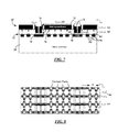
- FIG. 3 is an isometric view of a portion of an exemplary reconfigurable device, where the device includes a base substrate, a lower array and an upper array;
- FIGS. 4, 5 and 6 are plan views of a portion of the lower array of FIG. 3 , the upper array of FIG. 3 , and the combination of the lower and upper arrays, respectively;
- FIG. 7 is a sectional view of a portion of the reconfigurable device of FIG. 3 ;
- FIG. 8 is a plan view of a portion of the reconfigurable device of FIG. 3 ;
- FIG. 9 is a graph showing power transmission through the reconfigurable device of FIG. 3 , where the graph illustrates power transmission for both perfect and non-perfect contacts;
- FIG. 10 is a schematic view of a sequence of steps that may be used in a fabrication method to manufacture the reconfigurable device of FIG. 3 ;
- FIGS. 11A, 11B are enlarged scanning electron microscope (SEM) images of a particular embodiment of the exemplary reconfigurable device of FIG. 3 after it has been fabricated, with FIG. 11A being at ⁇ 900 magnification and FIG. 11B being at ⁇ 6,000 magnification;
- SEM scanning electron microscope
- FIGS. 12-14 are isometric views of portions of the reconfigurable device of FIG. 3 , where FIG. 12 is a portion of the device that includes a number of MEMS switches, FIG. 13 is an enlarged view of a single MEMS switch in the ‘OFF’ mode, and FIG. 14 is an enlarged view of the same MEMS switch but in the ‘ON’ mode; and
- FIGS. 15A-C are graphs showing the relative permeability, relative permittivity, and electromagnetic power transmission through the reconfigurable device of FIG. 3 for a horizontally-polarized incident electromagnetic wave, the graphs show the device in both an ‘OFF’ mode and an ‘ON’ mode.
- FIGS. 16A-D are graphs showing experimental results of a prototype modulator showing (a) the electric field of the transmitted THz pulse through the modulator, (b) the power transmission spectrum of a THz pulse incident on the modulator, (c) the modulation depth of the modulator, and (d) the dynamic characteristics of the modulator showing modulation depth as a function of modulation speed.
- a reconfigurable device as well as methods for fabricating and operating such a device, is described herein and is designed for use in the terahertz (THz) and infrared (IR) ranges. It should be appreciated that this device may operate in a number of different modes, including a filter mode and a separate modulation mode.
- a filter mode when the reconfigurable device is operating in a filter mode, it is sometimes referred to as a “reconfigurable filter,” and when the reconfigurable device is operating in a modulation mode, it is sometimes referred to as a “modulator.”
- the terms “reconfigurable filter” and “modulator” may be used interchangeably and are collectively or broadly referred to as a “reconfigurable device.”
- the reconfigurable device described herein meets high performance filtering and/or modulation specifications, such as those oftentimes required by high-performance imaging, spectroscopy, and communication systems.
- the modulator includes a mechanically reconfigurable multi-layer structure and can offer significant modulation depth and bandwidth, without considerable compromise in terms of modulation speed and voltage, in a fully integrated device configuration.
- a mechanically reconfigurable multi-layer filter that can reconfigure its geometry through the use of a double-layered mesh filter having an array of electrostatically-actuated micro-electrical-mechanical system (MEMS) switches that allow significant changes in the device scattering parameters over a broad range of frequencies.
- MEMS micro-electrical-mechanical system
- Some non-limiting examples of potential applications for the present reconfigurable filter or modulator include, but are certainly not limited to: high-performance THz and IR communication systems; high-performance THz and IR spectroscopy systems for chemical sensing and material characterization; THz and IR imaging systems for medical imaging, material characterization, and industrial quality control; and spatial beam forming for various applications including a single-pixel THz/IR camera through compressive sensing.
- the reconfigurable device may be employed in applications used by various security, military, environmental, scientific (e.g., biological, chemical, etc.), space study, pharmaceutical, and quality control industries, to cite a few possibilities. It should be appreciated that while the reconfigurable device described herein is directed to use in the THz and IR ranges, it is not limited to such and may be used with electromagnetic waves outside of these frequency and wavelength domains.
- FIG. 1 there is shown a schematic diagram of an exemplary terahertz (THz) system 10 that includes an optical pump 12 , a THz transmitter 14 , and an example of a reconfigurable filter or modulator 16 .
- THz terahertz
- the optical pump 12 illuminates or pumps the THz transmitter 14 with an optical beam 20 that causes the THz transmitter 14 to emit a first THz beam 22 .
- the first THz beam 22 is incident upon and is manipulated by reconfigurable device 16 so that a second filtered or modulated THz beam 24 is ultimately provided.
- FIGS. 2A and 2B illustrate the potential performance of such a system, where FIG.
- FIG. 2A shows the THz flux interaction 30 with the reconfigurable device 16 when the device is in an ‘OFF’ mode and FIG. 2B shows the THz flux interaction with the reconfigurable device 16 when the device is in an ‘ON’ mode.
- the degree to which the unfiltered THz beam 22 interacts with the reconfigurable device 16 is clearly much greater when the device is operating in the ‘ON’ mode, as illustrated by the graphs.
- FIG. 2A there is efficient electromagnetic flux transmission through the reconfigurable device 16 when the device is in a weak diamagnetic state
- FIG. 2B there is strong electromagnetic flux exclusion from the reconfigurable device region when it is in a strong diamagnetic state.
- the reconfigurable device 16 exhibits switchable diamagnetism so that it is able to dynamically switch or change modes over a broad range of THz and IR ranges.
- the reconfigurable device 16 is provided as a mechanically reconfigurable multi-layer filter and includes a base substrate 50 , a lower array 52 , and an upper array 54 .
- the reconfigurable device 16 can be provided as a modulator, a reconfigurable metasurface, a reconfigurable frequency selective surface, or a spatial beam modulator, to cite several possibilities.
- the base substrate 50 may be made of high resistivity silicon or any other suitable material known in the art and acts as an electrostatic actuation pad and a foundational substrate layer to which the different arrays or layers can be attached.
- electro-static switches are not the only possibility, as switches based on piezoelectric and/or magnetic materials may be used as well.
- the lower array 52 is a static or fixed array of conductive elements that are arranged in a mesh-like or periodic configuration on the base substrate 50 and act as contacts for the upper array 54 .
- the lower array 52 is mounted or fabricated on a surface of the base substrate 50 and includes a number of conductive element assemblies 60 (extend in x-z plane) that are somewhat tree-like in structure and are generally arranged so that they are parallel to one another.
- Each of the conductive element assemblies 60 further includes a number of long conductive elements or slits 62 (extend in z-axis direction) and short conductive elements or patches 64 (extend in x-axis direction), where the short conductive elements are attached to the long conductive elements in the form of cross-members and act as contact pads for cooperating elements of the upper array 52 , as will be explained.
- the long conductive elements 62 are arranged so that they are generally parallel to the other long conductive elements, and the short conductive elements 64 are arranged so that they are generally parallel to the other short conductive elements, thus, producing a periodic mesh-like array of conductive elements that together make up the lower array 52 .
- FIG. 4 as well as FIG.
- the + and ⁇ signs refer to the induced dipole moments as a result of the incident electromagnetic force on the metal electrons of the reconfigurable device 16
- the arrows refer to the induced surface current as a result of the incident electromagnetic force on the metal electrons of the lower and upper array components.
- the various elements of the lower array 52 may be made from any number of suitable conducting materials, including gold (Au) and gold-based alloys that are known in the art to be good conductors in MEMS switches.
- Each of the elements of the lower array 52 is attached to the base substrate 50 via an intervening insulation layer 70 , such as one made from SiO 2 (see FIG. 7 ), which electrically isolates the conductive elements of the lower array 52 from the base substrate 50 .
- the particular dimensions and sizes of the lower array 52 are largely dictated by the particular application and/or mode in which the reconfigurable device 16 is to be used, which takes into account the frequency or wavelength regimes involved and the operational parameters desired.
- the lower filter array 52 preferably has sub-wavelength dimensional spacing (i.e., the spacing between elements of the lower array is generally less than the wavelengths of the incident THz and IR waves).
- conductive element assemblies 60 may be spaced from one another by a distance (a) of approximately 16 ⁇ m
- the short conductive members 64 may be spaced from one another by a distance (b) of approximately 12 ⁇ m
- the short conductive members 64 may have a length (c) of approximately 9 ⁇ m.
- the distance (b) between the short conductive elements or contact pads 64 can have particular relevance, as this dimension along with other dimensions of elements 64 can influence the cutoff frequency and other operating characteristics of the reconfigurable filter 16 .
- the preceding dimensions are only meant to illustrate a potential scale and size of the elements involved and are in no way meant to limit the structure.
- the upper array 54 is a dynamic or flexible array of conductive elements that are arranged overtop of the lower array 52 and are designed to deflect towards and away from the lower array so that they selectively make or break contact with the lower array based on the state of the reconfigurable device 16 .
- the upper array 54 includes a number of flexible conductive elements 72 (extend in z-axis direction), anchor elements 74 (extend in y-axis direction), and contacts 76 located on the underside of the flexible conductive elements.
- Each of the flexible conductive elements 72 can bend and is suspended over the lower array 52 by a pair of anchor elements 74 located at each end so that the lower and upper arrays can act as a series of multi-contact micro-mechanical-electrical system (MEMS) switches.
- the anchor elements 74 act as century posts at each end of the flexible conductive element 72 and maintain the flexible conductive element in a suspended fashion so that it acts as a flexible beam or membrane suspended above and spaced from the lower array 52 ; the spacing is just enough so that application of a proper voltage to the reconfigurable device can cause the suspended beam to deflect towards the lower array 52 and establish an electrical connection there between.
- the flexible conductive elements 72 are arranged so that they are generally parallel to one another.
- the contacts 76 are formed on the underside of the flexible conductive elements 72 and are preferably provided as dimples or as other suitable shapes so that they can adequately establish an electrical connection with the corresponding short conductive elements 64 or other contact pads when element 72 flexes or deflects in that direction.
- This suspended beam configuration with elements 72 having a relatively long length may help accomplish several objectives: it accommodates multiple pairs of contacts 76 on the underside of each element 72 (e.g., four contact pairs) such that the spacing between contact pairs is relatively small, as is required for broadband operation at THz frequencies; it also provides for large actuation areas that are typically required for switch operation at low actuation voltages; and it simplifies biasing the two-dimensional array of MEMS switches with the small spacing required for broadband operation of the designed modulator, to cite a few examples.
- the contacts 76 are purposely designed to be non-perfect; that is, they are designed so that when a flexible conductive element 72 bends towards several short conductive elements 64 there is a very small gap between the two metallic elements (e.g., a gap of between 10-20 nm). This small gap may slightly impact the performance of the reconfigurable device, but it can greatly improve the robustness or durability of the flexible conductive elements 72 which will bend or deflect many, many times during the life of the device. As illustrated in FIG. 9 , the estimated transmission of a horizontally-polarized electromagnetic wave through the reconfigurable device 16 , as a function of the contact gap between the contacts 76 and the elements of the lower array 52 , is quite good. That graph demonstrates efficient transmission of the horizontally-polarized electromagnetic wave for contact gaps as small as 100 nm, as well as modulation depth levels of more than 90% for contact gaps as large as 10 nm.
- the various elements of the upper array 54 may also be made from any number of suitable conducting materials, including electroplated gold (Au) and gold-based alloys that are known in the art to be good conductors in MEMS switches.
- the anchor elements 74 are also attached to the base substrate 50 via an intervening insulation layer 70 , such as one made from SiO 2 (see FIG. 7 ), which electrically isolates the anchor elements 74 from the base substrate 50 .
- the particular dimensions and sizes of the arrays 54 are largely dictated by the particular mode and/or application in which the reconfigurable device 16 is to be used, which takes into account the frequency or wavelength regimes involved and the operational parameters desired.
- the upper array 54 preferably has sub-wavelength dimensional spacing (i.e., the spacing between elements of the upper array are generally less than the wavelengths of the incident THz and IR waves).
- the flexible conductive elements 72 i.e., the flexibly beams or membranes
- the flexible conductive elements 72 may have a length (d) of approximately 40 ⁇ m and a thickness (e) of approximately 1.25 ⁇ m
- the anchor elements 74 may have a height (f) of approximately 1.75 ⁇ m
- a contact gap or spacing (g) between the contacts 76 and the various conductive elements of the lower array 52 may be approximately 0.25 ⁇ m.
- the spacing between flexible elements may also be a distance (a) of approximately 16 ⁇ m, A relatively thick metal layer (e) of about 1.25 ⁇ m, for example, may help the flexible conductive elements 72 achieve flatness of the contact areas and high spring constants.
- the contact gap (g) between the upper and lower array elements is preferably selected to achieve low actuation voltages and high actuation speeds while accounting for possible bending of the flexible conductive elements 72 over time as a result of uncompensated stress of the elements 72 .
- the preceding dimensions are only meant to illustrate the potential scale and size of the elements involved and are in no way meant to limit the structure.
- FIG. 10 there is shown a sequence of schematic drawings that illustrate one potential embodiment of a fabrication method 100 that may be used to create the reconfigurable device described herein.
- method 100 fabricates the reconfigurable device 16 using a six-mask surface micromachining process on a high-resistivity Si wafer.
- the method generally starts by defining the actuation areas where the different conductive elements of the upper and lower arrays 52 , 54 are going to be formed on the base substrate 50 via the intervening insulation layer 70 .
- the actuation areas can be defined or otherwise created by silicon reactive ion etching or some other suitable etching technique.
- panel (b) shows a step of the method where the intervening insulation layer 70 is deposited in the voids or spaces that were etched in the previous step.
- Different techniques may be used to accomplish this deposition process, including using plasma enhanced chemical vapor deposition to deposit SiO 2 insulating pads or elements in the etched out spaces.
- the base substrate or wafer 50 may then be planarized using a chemical mechanical polishing technique to create a planar surface across the top of the base substrate.
- Various elements of the lower and upper arrays 52 , 54 , as well as any needed bias lines, may then be formed on the planarized surface of the base substrate 50 , as depicted in panel (c).
- One technique for carrying out this method step is a sputtering technique, such as one employing Ti/Au/Ti (100/1000/100 ⁇ ), followed by lift off. According to the example shown here, this step results in the formation of the conductive element assemblies 60 which are part of the lower array 52 , as well as contact pads 80 which are located underneath the anchor elements 74 and are part of the upper array 54 .
- the next step in the fabrication method is shown in panel (d) and involves applying a sacrificial layer 82 that is patterned for the subsequent creation of the anchor elements 74 and contacts or dimples 76 . More specifically, it is possible for this step to use a PMMA/PMGI sacrificial layer 82 (e.g., one about 0.5 ⁇ m thick) that is spin coated and patterned, as described above, using two separate masks.
- a sacrificial layer 82 e.g., one about 0.5 ⁇ m thick
- a thin layer 84 is deposited on top of the sacrificial layer 82 and acts as the seed layer for electroplating the various elements of the upper array 54 .
- This step is depicted in panel (e).
- the thin layer 84 is a Ti/Au layer (e.g., about 100/2500 ⁇ ) that is deposited on the sacrificial layer 82 using a suitable sputtering technique.
- a relatively thick gold (Au) layer (e.g., one about 1.0 ⁇ m thick) is electroplated for the anchor elements 74 and the thick metal part in the center of the flexible conductive elements 72 which are the flexible membranes mentioned above.
- the thin seed layer 84 and the sacrificial layer 82 are removed using a process, such as wet etching. More specifically, the thin seed layer 84 is removed except for areas under the MEMS switch.
- the reconfigurable device 16 which is shown in panel (g), can then be released using critical point drying or some other suitable technique.
- a rectangular metallic aperture of approximately 1 mm ⁇ 1 mm may be fabricated around the device prototypes to ensure that the transmitted terahertz (THz) power through the structure has fully interacted with the device active area.
- FIGS. 11A, 11B are scanning electron microscope (SEM) images of reconfigurable device 16 after it has been fabricated, with FIG. 11A ( ⁇ 900) showing a portion of the overall reconfigurable device and FIG. 11B ( ⁇ 6,000) showing an enlarged portion of the reconfigurable device so that electrostatically-actuated micro-electrical-mechanical system (MEMS) switches can be seen in more detail.
- SEM scanning electron microscope
- the reconfigurable device 16 is used to provide broadband, extreme diamagnetic switching at or near room temperature. By reshaping the structural configuration of the strongly coupled meta-molecule unit cells of the reconfigurable device 16 , their collective magnetic response to an incident electromagnetic wave can be altered.
- each of the MEMS switches in the device acts as a low-pass filter (capacitive mesh structure) for horizontally-polarized incident electromagnetic waves.
- the metal electrons in the modulator 16 cannot gain kinetic energy from the incident electromagnetic wave, as their acceleration path is constrained in the horizontal direction (x-axis direction).
- each of the MEMS switches in the reconfigurable device acts as a high-pass filter (inductive mesh structure) for horizontally-polarized incident electromagnetic waves.
- the metal electrons in the reconfigurable device 16 are able to gain kinetic energy from the incident electromagnetic wave since their acceleration path is not constrained in the horizontal direction (x-axis direction) by the combination of the upper and lower arrays in contact with one another. This creates a surface current that is illustrated by the arrows in FIG. 6 .
- the low-pass and high-pass filters mentioned above may exhibit similar cutoff frequencies due to the geometry of the reconfigurable device 16 .
- the flexible conductive element 72 of the upper array 54 (i.e., the flexible beam or membrane) is suspended over top of the conductive elements of the lower array 52 so that they are not in electrical contact with one another. Put differently, in this state the lower and upper arrays 52 , 54 are electrically isolated from one another.
- the incident electromagnetic wave creates a horizontal force on the metal electrons in both of the lower and upper arrays.
- both the lower and upper arrays 52 , 54 behave like low-pass or capacitive filters for horizontally-polarized incident electromagnetic waves, with a cutoff frequency that is inversely proportional to the periodicity and feature size of the arrays in the horizontal direction.
- the geometry of the lower and upper arrays 52 , 54 may be set to offer a cutoff frequency exceeding 3 THz for the combination of the two arrays when operating as capacitive structures; this can achieve efficient transmission of horizontally-polarized electromagnetic waves over a broad range of THz frequencies during the modulation ‘OFF’ mode.
- the reconfigurable device 16 exhibits diamagnetic switching capability, as it can switch between a weak diamagnetic state (modulation OFF) and a strong diamagnetic state (modulation ON).
- a weak diamagnetic state modulation OFF
- a strong diamagnetic state modulation ON
- the dimensions of the reconfigurable device can be specifically selected to achieve low switching voltages (e.g., about 30 V) and high switching speeds (e.g., >20 KHz), while accounting for possible bending in the flexible conductive elements 76 as a result of uncompensated stress of those membranes.
- Other considerations could also be taken into account, of course, when designing the reconfigurable device described herein.
- the electrical voltage could be applied to either array or layer; in those embodiments where the upper and lower arrays are electrically isolated from one another, then it is preferable to apply the voltage to the upper array to electrostatically deflect the switch.
- the flexible conductive element 72 of the upper array 54 deflects towards and contacts the conductive elements of the lower array 52 so that they are in electrical contact with one another.
- the combined lower and upper arrays 52 , 54 in contact with each other form a two-dimensional array of metallic loops or elements, as demonstrated by the representation in FIG. 6 .
- the strength of the induced magnetic field in response to the horizontally-polarized incident electromagnetic wave is strong for sub-wavelength unit cell sizes in the vertical direction (z-axis direction). This strong diamagnetic behavior is the result of efficient energy transfer from the incident electromagnetic wave to the kinetic energy of the metal electrons, producing an opposing magnetic filed that cancels the incident field in this region of the reconfigurable device.
- the lower and/or upper array elements e.g., if the spacing (b) between short conductive elements 64 ) in the vertical direction (z-axis direction) are much smaller than the incident electromagnetic wavelength, a large fraction of the incident electromagnetic energy will be converted to the kinetic energy of the metal electrons, which re-radiate the incident electromagnetic wave in the opposite direction, leading to a significant drop in the electromagnetic transmission through the reconfigurable device or surface.
- the lower and upper arrays 52 , 54 can behave like a high-pass filter (inductive structure) with a cutoff frequency that is inversely proportional to the periodicity of the short conductive elements 64 in the vertical or z-axis direction.
- the reconfigurable device 16 exhibits permeability over a 1.5 THz frequency band from ⁇ r >0.9 to ⁇ r ⁇ 7 ⁇ 10 ⁇ 3 ;
- the reconfigurable device 16 exhibits a similar permittivity behavior over a 1.5 THz frequency band;
- the reconfigurable device or surface modulates the intensity of terahertz (THz) waves with more than 90% modulation depth over a 1.5 THz frequency band.
- THz terahertz
- the reconfigurable device 16 described herein can offer broadband diamagnetic switching through structural miniaturization.
- FIGS. 16A-D is based on a proof-of-concept terahertz (THz) modulator having a reconfigurable device or surface with diamagnetic switching capability.
- FIG. 16A illustrates the electric field of a transmitted THz pulse through the modulator at a bias voltage of 0 V (modulation ‘OFF’ mode) and 30 V (modulation ‘ON’ mode).
- the OFF mode is represented by curve 160 and the ON mode is represented by curve 162 .
- FIG. 16B shows the power transmission spectrum of a THz pulse incident on the modulator over a 1.5 THz frequency range during the modulation ON and OFF modes.
- FIGS. 16D illustrates the dynamic characteristics of the modulator, characterized by measuring the electric field of the transmitted THz pulses through the modulator while alternating the bias voltage between 0 V and 30 V.
- the calculated THz modulation depth as a function of the modulation speed indicates modulations speeds exceeding 20 KHz.
- the lower and upper arrays 52 , 54 behave like inductive mesh filters for vertically-polarized electromagnetic waves independent of the operational mode or state of the reconfigurable device. This prevents transmission of a major fraction of vertically-polarized electromagnetic waves through the reconfigurable device and, therefore, offers a polarization-sensitive modulation or filter performance that is required for many imaging applications.
- the terms “for example,” “e.g.,” “for instance,” “such as,” and “like,” and the verbs “comprising,” “having,” “including,” and their other verb forms, when used in conjunction with a listing of one or more components or other items, are each to be construed as open-ended, meaning that that the listing is not to be considered as excluding other, additional components or items.
- Other terms are to be construed using their broadest reasonable meaning unless they are used in a context that requires a different interpretation.
Landscapes
- Physics & Mathematics (AREA)
- Electromagnetism (AREA)
- General Physics & Mathematics (AREA)
- Optics & Photonics (AREA)
- Engineering & Computer Science (AREA)
- Manufacturing & Machinery (AREA)
- Micromachines (AREA)
Abstract
Description
Claims (14)
Priority Applications (1)
| Application Number | Priority Date | Filing Date | Title |
|---|---|---|---|
| US14/910,523 US9859079B2 (en) | 2013-08-06 | 2014-08-06 | Reconfigurable device for terahertz (THz) and infrared (IR) filtering and modulation |
Applications Claiming Priority (3)
| Application Number | Priority Date | Filing Date | Title |
|---|---|---|---|
| US201361862730P | 2013-08-06 | 2013-08-06 | |
| PCT/US2014/049866 WO2015021100A1 (en) | 2013-08-06 | 2014-08-06 | Reconfigurable device for terahertz (thz) and infrared (ir) filtering and modulation |
| US14/910,523 US9859079B2 (en) | 2013-08-06 | 2014-08-06 | Reconfigurable device for terahertz (THz) and infrared (IR) filtering and modulation |
Publications (2)
| Publication Number | Publication Date |
|---|---|
| US20160196943A1 US20160196943A1 (en) | 2016-07-07 |
| US9859079B2 true US9859079B2 (en) | 2018-01-02 |
Family
ID=52461890
Family Applications (1)
| Application Number | Title | Priority Date | Filing Date |
|---|---|---|---|
| US14/910,523 Active US9859079B2 (en) | 2013-08-06 | 2014-08-06 | Reconfigurable device for terahertz (THz) and infrared (IR) filtering and modulation |
Country Status (2)
| Country | Link |
|---|---|
| US (1) | US9859079B2 (en) |
| WO (1) | WO2015021100A1 (en) |
Cited By (10)
| Publication number | Priority date | Publication date | Assignee | Title |
|---|---|---|---|---|
| US10790699B2 (en) | 2015-09-24 | 2020-09-29 | Apple Inc. | Configurable wireless transmitter device |
| US10863895B2 (en) | 2015-05-27 | 2020-12-15 | The Regents Of The University Of California | Terahertz endoscopy through laser-driven terahertz sources and detectors |
| US11112305B2 (en) | 2012-01-23 | 2021-09-07 | The Regents Of The University Of California | Photoconductive detector device with plasmonic electrodes |
| US11249017B2 (en) | 2017-04-20 | 2022-02-15 | The Regents Of The University Of California | Systems and methods for high frequency nanoscopy |
| US11456392B2 (en) | 2017-06-01 | 2022-09-27 | The Regents Of The University Of California | Metallo-graphene nanocomposites and methods for using metallo-graphene nanocomposites for electromagnetic energy conversion |
| US11843171B2 (en) | 2020-08-18 | 2023-12-12 | Samsung Electronics Co., Ltd. | Multi-layer reconfigurable surface for an antenna |
| US11906424B2 (en) | 2019-10-01 | 2024-02-20 | The Regents Of The University Of California | Method for identifying chemical and structural variations through terahertz time-domain spectroscopy |
| US11979030B2 (en) | 2016-08-26 | 2024-05-07 | Apple Inc. | Shared power converter for a wireless transmitter device |
| US12066380B2 (en) | 2019-10-31 | 2024-08-20 | The Regents Of The University Of California | Methods and systems for detecting water status in plants using terahertz radiation |
| US12498615B2 (en) | 2020-12-01 | 2025-12-16 | The Regents Of The University Of California | Systems and methods for wavelength conversion through plasmon-coupled surface states |
Families Citing this family (13)
| Publication number | Priority date | Publication date | Assignee | Title |
|---|---|---|---|---|
| US10044232B2 (en) | 2014-04-04 | 2018-08-07 | Apple Inc. | Inductive power transfer using acoustic or haptic devices |
| US10135303B2 (en) | 2014-05-19 | 2018-11-20 | Apple Inc. | Operating a wireless power transfer system at multiple frequencies |
| HK1253268A1 (en) | 2015-09-24 | 2019-06-14 | 苹果公司 | Configurable wireless transmitter device |
| US10477741B1 (en) * | 2015-09-29 | 2019-11-12 | Apple Inc. | Communication enabled EMF shield enclosures |
| US10651685B1 (en) | 2015-09-30 | 2020-05-12 | Apple Inc. | Selective activation of a wireless transmitter device |
| CN106058390B (en) * | 2016-07-08 | 2018-09-11 | 桂林电子科技大学 | A kind of Terahertz bandstop filter being adjusted by electrostatic drive |
| US10594160B2 (en) | 2017-01-11 | 2020-03-17 | Apple Inc. | Noise mitigation in wireless power systems |
| US10763290B2 (en) * | 2017-02-22 | 2020-09-01 | Elwha Llc | Lidar scanning system |
| RU2650343C1 (en) * | 2017-03-20 | 2018-04-11 | Государственное образовательное учреждение высшего профессионального образования Кыргызско-Российский Славянский университет (КРСУ) | Converter of terahertz vibrations into terahertz electromagnetic radiation |
| US10649303B2 (en) | 2017-04-28 | 2020-05-12 | Samsung Electronics Co., Ltd. | Optical device and optical system including the same |
| CN108319040A (en) * | 2018-01-23 | 2018-07-24 | 中国计量大学 | A kind of automatically controlled THz wave switch of more metal layers structure |
| CN109489815A (en) * | 2018-03-13 | 2019-03-19 | 电子科技大学 | Light-operated flexible semiconductor THz wave spatial modulator |
| CN113008907B (en) * | 2019-12-19 | 2024-04-12 | 华为技术有限公司 | Terahertz sensing system and terahertz sensing array |
Citations (8)
| Publication number | Priority date | Publication date | Assignee | Title |
|---|---|---|---|---|
| US6529093B2 (en) * | 2001-07-06 | 2003-03-04 | Intel Corporation | Microelectromechanical (MEMS) switch using stepped actuation electrodes |
| US20050236260A1 (en) | 2004-01-29 | 2005-10-27 | Rolltronics Corporation | Micro-electromechanical switch array |
| US20070278075A1 (en) * | 2004-07-29 | 2007-12-06 | Akihisa Terano | Capacitance Type Mems Device, Manufacturing Method Thereof, And High Frequency Device |
| US20080001691A1 (en) | 2006-06-29 | 2008-01-03 | Samsung Electronics Co., Ltd. | MEMS switch and method of fabricating the same |
| KR20080004467A (en) | 2005-03-21 | 2008-01-09 | 델프멤스 | Radio frequency microelectromechanical system switches with flexible and free switch membranes |
| US7321275B2 (en) * | 2005-06-23 | 2008-01-22 | Intel Corporation | Ultra-low voltage capable zipper switch |
| US20080277672A1 (en) | 2007-05-07 | 2008-11-13 | Innovative Micro Technology | Lid structure for microdevice and method of manufacture |
| US20120122259A1 (en) | 2006-06-30 | 2012-05-17 | Qualcomm Mems Technologies, Inc. | Method of manufacturing mems devices providing air gap control |
-
2014
- 2014-08-06 WO PCT/US2014/049866 patent/WO2015021100A1/en not_active Ceased
- 2014-08-06 US US14/910,523 patent/US9859079B2/en active Active
Patent Citations (9)
| Publication number | Priority date | Publication date | Assignee | Title |
|---|---|---|---|---|
| US6529093B2 (en) * | 2001-07-06 | 2003-03-04 | Intel Corporation | Microelectromechanical (MEMS) switch using stepped actuation electrodes |
| US20050236260A1 (en) | 2004-01-29 | 2005-10-27 | Rolltronics Corporation | Micro-electromechanical switch array |
| US20070278075A1 (en) * | 2004-07-29 | 2007-12-06 | Akihisa Terano | Capacitance Type Mems Device, Manufacturing Method Thereof, And High Frequency Device |
| KR20080004467A (en) | 2005-03-21 | 2008-01-09 | 델프멤스 | Radio frequency microelectromechanical system switches with flexible and free switch membranes |
| US7834722B2 (en) | 2005-03-21 | 2010-11-16 | Delfmems | RF MEMS switch with a flexible and free switch membrane |
| US7321275B2 (en) * | 2005-06-23 | 2008-01-22 | Intel Corporation | Ultra-low voltage capable zipper switch |
| US20080001691A1 (en) | 2006-06-29 | 2008-01-03 | Samsung Electronics Co., Ltd. | MEMS switch and method of fabricating the same |
| US20120122259A1 (en) | 2006-06-30 | 2012-05-17 | Qualcomm Mems Technologies, Inc. | Method of manufacturing mems devices providing air gap control |
| US20080277672A1 (en) | 2007-05-07 | 2008-11-13 | Innovative Micro Technology | Lid structure for microdevice and method of manufacture |
Non-Patent Citations (2)
| Title |
|---|
| International Search Report for application No. PCT/US2014/049866 dated Nov. 20, 2014, 3 pages. |
| Written Opinion for application No. PCT/US2014/049866 dated Nov. 20, 2014, 6 pages. |
Cited By (11)
| Publication number | Priority date | Publication date | Assignee | Title |
|---|---|---|---|---|
| US11112305B2 (en) | 2012-01-23 | 2021-09-07 | The Regents Of The University Of California | Photoconductive detector device with plasmonic electrodes |
| US11231318B2 (en) | 2012-01-23 | 2022-01-25 | The Regents Of The University Of California | Photoconductive detector device with plasmonic electrodes |
| US10863895B2 (en) | 2015-05-27 | 2020-12-15 | The Regents Of The University Of California | Terahertz endoscopy through laser-driven terahertz sources and detectors |
| US10790699B2 (en) | 2015-09-24 | 2020-09-29 | Apple Inc. | Configurable wireless transmitter device |
| US11979030B2 (en) | 2016-08-26 | 2024-05-07 | Apple Inc. | Shared power converter for a wireless transmitter device |
| US11249017B2 (en) | 2017-04-20 | 2022-02-15 | The Regents Of The University Of California | Systems and methods for high frequency nanoscopy |
| US11456392B2 (en) | 2017-06-01 | 2022-09-27 | The Regents Of The University Of California | Metallo-graphene nanocomposites and methods for using metallo-graphene nanocomposites for electromagnetic energy conversion |
| US11906424B2 (en) | 2019-10-01 | 2024-02-20 | The Regents Of The University Of California | Method for identifying chemical and structural variations through terahertz time-domain spectroscopy |
| US12066380B2 (en) | 2019-10-31 | 2024-08-20 | The Regents Of The University Of California | Methods and systems for detecting water status in plants using terahertz radiation |
| US11843171B2 (en) | 2020-08-18 | 2023-12-12 | Samsung Electronics Co., Ltd. | Multi-layer reconfigurable surface for an antenna |
| US12498615B2 (en) | 2020-12-01 | 2025-12-16 | The Regents Of The University Of California | Systems and methods for wavelength conversion through plasmon-coupled surface states |
Also Published As
| Publication number | Publication date |
|---|---|
| WO2015021100A1 (en) | 2015-02-12 |
| US20160196943A1 (en) | 2016-07-07 |
Similar Documents
| Publication | Publication Date | Title |
|---|---|---|
| US9859079B2 (en) | Reconfigurable device for terahertz (THz) and infrared (IR) filtering and modulation | |
| KR101647045B1 (en) | 3-dimensional standing type metamaterial structure and method of fabricating the same | |
| Pitchappa et al. | Frequency‐agile temporal terahertz metamaterials | |
| US7486002B2 (en) | Lateral piezoelectric driven highly tunable micro-electromechanical system (MEMS) inductor | |
| JP5701772B2 (en) | Via structure and manufacturing method thereof | |
| Unlu et al. | Switchable scattering meta-surfaces for broadband terahertz modulation | |
| US7098577B2 (en) | Piezoelectric switch for tunable electronic components | |
| US20070164839A1 (en) | Electric machine signal selecting element | |
| US20140111811A1 (en) | Micromechanical tunable fabry-perot interferometer and a method for producing the same | |
| US20170113928A1 (en) | Device and method for producing a device comprising micro or nanostructures | |
| WO2008071172A1 (en) | Micromirror actuator with encapsulation possibility and method for production thereof | |
| CN102656649A (en) | Two-terminal variable capacitance MEMS device | |
| CN104737365A (en) | Directional couplers with variable frequency response | |
| US7042397B2 (en) | Phase-shifting cell for an antenna reflectarray | |
| KR20020032585A (en) | Acoustic wave device comprising alternating polarization domains | |
| US8421305B2 (en) | MEMS devices and systems actuated by an energy field | |
| Huang et al. | MEMS-actuated terahertz metamaterials driven by phase-transition materials | |
| US20230013976A1 (en) | Movable piezo element and method for producing a movable piezo element | |
| JP2006147540A (en) | Electromechanical switch | |
| Honma et al. | Free‐standing aluminium nanowire arrays for high‐transmission plasmonic colour filters | |
| US20140203896A1 (en) | Tunable Cavity Resonator Including A Plurality of MEMS Beams | |
| Valente | Fabrication of planar nanomechanical photonic metamaterials | |
| KR20090053103A (en) | RF switch | |
| Unlu et al. | Broadband terahertz modulators based on MEMS-reconfigurable mesh filters | |
| KR101445028B1 (en) | Silicon Nitride Scanner with Improved Tilt Angl and Manufacturing Method thereof |
Legal Events
| Date | Code | Title | Description |
|---|---|---|---|
| STCF | Information on status: patent grant |
Free format text: PATENTED CASE |
|
| AS | Assignment |
Owner name: NATIONAL SCIENCE FOUNDATION, VIRGINIA Free format text: CONFIRMATORY LICENSE;ASSIGNOR:UNIVERSITY OF MICHIGAN;REEL/FRAME:048383/0139 Effective date: 20190130 |
|
| AS | Assignment |
Owner name: THE REGENTS OF THE UNIVERSITY OF MICHIGAN, MICHIGA Free format text: ASSIGNMENT OF ASSIGNORS INTEREST;ASSIGNORS:JARRAHI, MONA;UNLU, MEHMET;BERRY, CHRISTOPHER W.;AND OTHERS;SIGNING DATES FROM 20150128 TO 20150130;REEL/FRAME:050682/0295 |
|
| AS | Assignment |
Owner name: THE REGENTS OF THE UNIVERSITY OF CALIFORNIA, CALIF Free format text: ASSIGNMENT OF ASSIGNORS INTEREST;ASSIGNOR:THE REGENTS OF THE UNIVERSITY OF MICHIGAN;REEL/FRAME:050708/0091 Effective date: 20190924 |
|
| CC | Certificate of correction | ||
| MAFP | Maintenance fee payment |
Free format text: PAYMENT OF MAINTENANCE FEE, 4TH YR, SMALL ENTITY (ORIGINAL EVENT CODE: M2551); ENTITY STATUS OF PATENT OWNER: SMALL ENTITY Year of fee payment: 4 |
|
| FEPP | Fee payment procedure |
Free format text: 7.5 YR SURCHARGE - LATE PMT W/IN 6 MO, SMALL ENTITY (ORIGINAL EVENT CODE: M2555); ENTITY STATUS OF PATENT OWNER: SMALL ENTITY |
|
| MAFP | Maintenance fee payment |
Free format text: PAYMENT OF MAINTENANCE FEE, 8TH YR, SMALL ENTITY (ORIGINAL EVENT CODE: M2552); ENTITY STATUS OF PATENT OWNER: SMALL ENTITY Year of fee payment: 8 |