US9858952B1 - Microwave assisted magnetic recording head having spin torque oscillator frequency detection - Google Patents
Microwave assisted magnetic recording head having spin torque oscillator frequency detection Download PDFInfo
- Publication number
- US9858952B1 US9858952B1 US15/199,833 US201615199833A US9858952B1 US 9858952 B1 US9858952 B1 US 9858952B1 US 201615199833 A US201615199833 A US 201615199833A US 9858952 B1 US9858952 B1 US 9858952B1
- Authority
- US
- United States
- Prior art keywords
- magnetic
- layer
- spin torque
- torque oscillator
- barrier layer
- Prior art date
- Legal status (The legal status is an assumption and is not a legal conclusion. Google has not performed a legal analysis and makes no representation as to the accuracy of the status listed.)
- Active
Links
- 238000001514 detection method Methods 0.000 title abstract 2
- 230000010287 polarization Effects 0.000 claims abstract description 13
- 239000010410 layer Substances 0.000 claims description 115
- 230000004888 barrier function Effects 0.000 claims description 30
- 230000008859 change Effects 0.000 claims description 6
- 229910019092 Mg-O Inorganic materials 0.000 claims description 5
- 229910019395 Mg—O Inorganic materials 0.000 claims description 5
- 239000011229 interlayer Substances 0.000 claims description 5
- 230000010355 oscillation Effects 0.000 abstract description 25
- 239000000654 additive Substances 0.000 abstract description 5
- 230000000996 additive effect Effects 0.000 abstract description 5
- 238000004519 manufacturing process Methods 0.000 description 7
- 230000005415 magnetization Effects 0.000 description 6
- 239000000725 suspension Substances 0.000 description 6
- 239000000463 material Substances 0.000 description 5
- PNEYBMLMFCGWSK-UHFFFAOYSA-N aluminium oxide Inorganic materials [O-2].[O-2].[O-2].[Al+3].[Al+3] PNEYBMLMFCGWSK-UHFFFAOYSA-N 0.000 description 3
- 230000004907 flux Effects 0.000 description 3
- 238000000034 method Methods 0.000 description 3
- 230000008569 process Effects 0.000 description 3
- 229910052802 copper Inorganic materials 0.000 description 2
- 239000012777 electrically insulating material Substances 0.000 description 2
- 229910052737 gold Inorganic materials 0.000 description 2
- 238000005498 polishing Methods 0.000 description 2
- 238000007493 shaping process Methods 0.000 description 2
- 239000000126 substance Substances 0.000 description 2
- 230000005641 tunneling Effects 0.000 description 2
- 229910019236 CoFeB Inorganic materials 0.000 description 1
- 230000000712 assembly Effects 0.000 description 1
- 238000000429 assembly Methods 0.000 description 1
- 239000002800 charge carrier Substances 0.000 description 1
- 238000004590 computer program Methods 0.000 description 1
- 239000004020 conductor Substances 0.000 description 1
- 230000008878 coupling Effects 0.000 description 1
- 238000010168 coupling process Methods 0.000 description 1
- 238000005859 coupling reaction Methods 0.000 description 1
- 230000001737 promoting effect Effects 0.000 description 1
- 230000004044 response Effects 0.000 description 1
- 238000000992 sputter etching Methods 0.000 description 1
- 239000002699 waste material Substances 0.000 description 1
Images


Classifications
-
- G—PHYSICS
- G11—INFORMATION STORAGE
- G11B—INFORMATION STORAGE BASED ON RELATIVE MOVEMENT BETWEEN RECORD CARRIER AND TRANSDUCER
- G11B5/00—Recording by magnetisation or demagnetisation of a record carrier; Reproducing by magnetic means; Record carriers therefor
- G11B5/127—Structure or manufacture of heads, e.g. inductive
- G11B5/31—Structure or manufacture of heads, e.g. inductive using thin films
- G11B5/3109—Details
- G11B5/313—Disposition of layers
- G11B5/3133—Disposition of layers including layers not usually being a part of the electromagnetic transducer structure and providing additional features, e.g. for improving heat radiation, reduction of power dissipation, adaptations for measurement or indication of gap depth or other properties of the structure
- G11B5/314—Disposition of layers including layers not usually being a part of the electromagnetic transducer structure and providing additional features, e.g. for improving heat radiation, reduction of power dissipation, adaptations for measurement or indication of gap depth or other properties of the structure where the layers are extra layers normally not provided in the transducing structure, e.g. optical layers
-
- G—PHYSICS
- G11—INFORMATION STORAGE
- G11B—INFORMATION STORAGE BASED ON RELATIVE MOVEMENT BETWEEN RECORD CARRIER AND TRANSDUCER
- G11B5/00—Recording by magnetisation or demagnetisation of a record carrier; Reproducing by magnetic means; Record carriers therefor
- G11B5/127—Structure or manufacture of heads, e.g. inductive
- G11B5/33—Structure or manufacture of flux-sensitive heads, i.e. for reproduction only; Combination of such heads with means for recording or erasing only
- G11B5/39—Structure or manufacture of flux-sensitive heads, i.e. for reproduction only; Combination of such heads with means for recording or erasing only using magneto-resistive devices or effects
- G11B5/3903—Structure or manufacture of flux-sensitive heads, i.e. for reproduction only; Combination of such heads with means for recording or erasing only using magneto-resistive devices or effects using magnetic thin film layers or their effects, the films being part of integrated structures
- G11B5/3906—Details related to the use of magnetic thin film layers or to their effects
- G11B5/3912—Arrangements in which the active read-out elements are transducing in association with active magnetic shields, e.g. magnetically coupled shields
-
- G—PHYSICS
- G11—INFORMATION STORAGE
- G11B—INFORMATION STORAGE BASED ON RELATIVE MOVEMENT BETWEEN RECORD CARRIER AND TRANSDUCER
- G11B5/00—Recording by magnetisation or demagnetisation of a record carrier; Reproducing by magnetic means; Record carriers therefor
- G11B5/127—Structure or manufacture of heads, e.g. inductive
- G11B5/31—Structure or manufacture of heads, e.g. inductive using thin films
- G11B5/3109—Details
- G11B5/313—Disposition of layers
- G11B5/3143—Disposition of layers including additional layers for improving the electromagnetic transducing properties of the basic structure, e.g. for flux coupling, guiding or shielding
- G11B5/3146—Disposition of layers including additional layers for improving the electromagnetic transducing properties of the basic structure, e.g. for flux coupling, guiding or shielding magnetic layers
-
- G—PHYSICS
- G11—INFORMATION STORAGE
- G11B—INFORMATION STORAGE BASED ON RELATIVE MOVEMENT BETWEEN RECORD CARRIER AND TRANSDUCER
- G11B5/00—Recording by magnetisation or demagnetisation of a record carrier; Reproducing by magnetic means; Record carriers therefor
- G11B5/127—Structure or manufacture of heads, e.g. inductive
- G11B5/31—Structure or manufacture of heads, e.g. inductive using thin films
- G11B5/3163—Fabrication methods or processes specially adapted for a particular head structure, e.g. using base layers for electroplating, using functional layers for masking, using energy or particle beams for shaping the structure or modifying the properties of the basic layers
-
- G—PHYSICS
- G11—INFORMATION STORAGE
- G11B—INFORMATION STORAGE BASED ON RELATIVE MOVEMENT BETWEEN RECORD CARRIER AND TRANSDUCER
- G11B5/00—Recording by magnetisation or demagnetisation of a record carrier; Reproducing by magnetic means; Record carriers therefor
- G11B2005/0002—Special dispositions or recording techniques
- G11B2005/0005—Arrangements, methods or circuits
- G11B2005/0024—Microwave assisted recording
Definitions
- the present invention relates to magnetic data recording, and more particularly to a magnetic write head having a magnetic spin torque oscillator located between a magnetic write pole and a magnetic trailing shield and having a structure for detecting the magnetic oscillation frequency of the spin torque oscillator.
- the magnetic disk drive includes a rotating magnetic disk, write and read heads that are suspended by a suspension arm adjacent to a surface of the rotating magnetic disk and an actuator that swings the suspension arm to place the read and write heads over selected tracks on the rotating disk.
- the read and write heads are directly located on a slider that has an air bearing surface (ABS).
- ABS air bearing surface
- the suspension arm biases the slider into contact with the surface of the disk when the disk is not rotating, but when the disk rotates air is swirled by the rotating disk.
- the write and read heads are employed for writing magnetic impressions to and reading magnetic impressions from the rotating disk.
- the write and read heads are connected to processing circuitry that operates according to a computer program to implement the writing and reading functions.
- a magnetoresistive sensor such as a Giant Magnetoresistive (GMR) sensor, a Tunnel Junction Magnetoresistive (TMR) sensor or a scissor type magnetoresistive sensor can be employed to read a magnetic signal from the magnetic media.
- the magnetoresistive sensor has an electrical resistance that changes in response to an external magnetic field. This change in electrical resistance can be detected by processing circuitry in order to read magnetic data from the magnetic media.
- the magnetic sensor formed at the side of the spin torque oscillator advantageously detects magnetic field from the spin torque oscillator in order to accurately determine the oscillation frequency of the oscillating magnetic field produced by the spin torque oscillator.
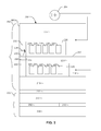
- FIG. 1 is a schematic illustration of a disk drive system in which the invention might be embodied
- FIG. 2 is side, cross-sectional, schematic view of a magnetic read write head
- FIGS. 5-7 are views of a spin torque oscillator in various intermediate stages of manufacture illustrating a method of manufacturing a spin torque oscillator according to an embodiment.
- the disk drive 100 includes a housing 101 . At least one rotatable magnetic disk 112 is supported on a spindle 114 and rotated by a disk drive motor 118 .
- the magnetic recording on each disk may be in the form of annular patterns of concentric data tracks (not shown) on the magnetic disk 112 .
- the rotation of the magnetic disk 112 generates an air bearing between the slider 113 and the disk surface 122 , which exerts an upward force or lift on the slider.
- the air bearing thus counter-balances the slight spring force of the suspension 115 and supports the slider 113 off and slightly above the disk surface by a small, substantially constant spacing during normal operation.
- control unit 129 The various components of the disk storage system are controlled in operation by control signals generated by control unit 129 , such as access control signals and internal clock signals.
- control unit 129 comprises logic control circuits, and a microprocessor.
- the control unit 129 generates control signals to control various system operations such as drive motor control signals on line 123 and head position and seek control signals on line 128 .
- the control signals on line 128 provide the desired current profiles to optimally move and position the slider 113 to the desired data track on the media 112 .
- Write and read signals are communicated to and from write and read heads 121 by way of recording channel 125 .
- a magnetic read/write head 200 can include a read head 202 and a write head 204 .
- the read head 202 can include a read sensor 206 such as a giant magnetoresistive sensor or tunnel junction sensor, which can be sandwiched between first and second magnetic shields 208 , 210 .
- the space between the read and write heads 202 , 204 can be filled with a non-magnetic, electrically insulating material 212 , as can the space behind the sensor 206 between the shields 208 , 210 .
- the write head 204 can include a magnetic write pole 214 and a magnetic return pole 216 , both of which can extend to a media facing surface MFS.
- the magnetic return pole 216 can be connected with the magnetic write pole 214 by a magnetic back gap layer 218 and a magnetic shaping layer 220 .
- the magnetic shaping layer 220 helps to channel magnetic flux to the tip of the magnetic write pole 214 .
- the write head 204 can also include a trailing magnetic shield 222 formed near the trailing edge of the write pole 214 at the media facing surface MFS.
- the trailing magnetic shield 222 can be connected with the back portion of the write head 204 by a trailing magnetic return pole 224 .
- the write head 204 also includes a non-magnetic, electrically conductive write coil 226 (shown in cross section in FIG. 2 ) that can pass above and below the write pole 214 .
- the write coil 226 can be embedded in a non-magnetic, electrically insulating material such as alumina 228 .
- a magnetic field is generated. This causes a magnetic flux to flow through the write pole 214 .
- the resulting write field travels from the tip of the write pole 214 to a magnetic media (not shown in FIG. 2 ) and then travels back through the return pole 216 . Because the return pole 216 has a larger cross section at the media facing surface MFS than does the write pole 214 , the return of the magnetic write field to the return pole 216 does not erase the previously recorded bit of data.
- the magnetic bits recorded to a recording media become inherently, magnetically unstable.
- the magnetic media can be designed to have an increased magnetic anisotropy, and or magnetic coercivity. This however makes the media harder to record to, especially with the smaller write pole required to record the smaller magnetic bit.
- a magnetic oscillator such as a spin torque oscillator 230 can be employed.
- the spin torque oscillator 230 can be located between the write pole 214 and the trailing magnetic shield 222 .
- the spin torque oscillator 230 generates an oscillating magnetic field that moves in a precessional manner as indicated by arrow 308 .
- a current source 234 can be provided to supply an electrical current to flow through the spin torque oscillator 230 .
- the current source 234 can be connected with the magnetic write head 204 so that current flows between the write pole 214 and the trailing shield 222 through the spin torque oscillator 230 . This current causes the spin torque oscillator to generate the oscillating magnetic field 308 .
- An electrically insulating layer 235 can be provided at the back of the write head 204 to prevent this electrical current from being shunted through the back portion of the write head 204 .
- FIG. 3 shows an enlarged view of the spin torque oscillator 230 according to one embodiment.
- the spin torque oscillator 230 includes two magnetic layers 302 , 304 separated by a non-magnetic interlayer 306 located between the magnetic layers 302 , 304 .
- the first magnetic layer 302 is a spin polarization layer
- the second magnetic layer 304 is a magnetic field generation layer.
- spin polarized electrons flow from the spin polarization layer 302 , through the interlayer 306 to the field generation layer 304 , they impart a spin torque on the field generation layer 304 .
- This spin torque causes the magnetization of the field generation layer 304 to oscillate as indicated by arrow 308 .
- the magnetic oscillation 308 of the field generation layer 304 can impart an oscillation 314 in the spin polarization layer 302 as a result of magnetostatic coupling between the magnetic layers 302 , 304 .
- the spin torque oscillator 230 may also include a seed layer 310 to promote a desired grain structure in the above formed layers 302 , 304 , 306 and may also include a capping layer 312 at the end opposite the seed layer 310 .
- An important design parameter for magnetic recording systems that employ spin torque oscillators is the frequency of the magnetic oscillation of the spin torque oscillation.
- a magnetic media has an optimal magnetic frequency oscillation range for promoting the writing of magnetic data to the magnetic media. Therefore, in order to maximize writing efficiency, the magnetic oscillation frequency of the spin torque oscillator is preferably matched to the magnetic media of the magnetic recording system.
- the write head is provided with tunnel junction magnetic sensors 316 formed at the sides of (or behind the spin torque oscillator 230 .
- the tunnel junction magnetic sensor 316 can be at one side, or can be at both sides of the sensor as shown.
- the magnetic tunnel junction sensor 316 includes a non-magnetic barrier layer 318 , a magnetic layer 320 and a non-magnetic, electrically conductive side lead 322 .
- the side lead 322 is electrically insulated from the shield 222 by an electrically insulating layer 325 , which may be a material such as alumina.
- the non-magnetic barrier layer 318 can be a material such as Mg—O, and as shown in FIG. 3 , the non-magnetic barrier layer 318 can be thicker over the write pole 214 and thinner along the side of the spin torque oscillator 230 .
- the thicker barrier layer 214 over the write pole 214 will prevent current shunting to the write pole 214 , and the barrier layer 318 should be thin enough along the side of the spin torque oscillator 230 to allow quantum tunneling of charge carriers there-through in a manner similar to a standard tunnel junction magnetic sensor as might be used to read a magnetic signal from a magnetic media.
- the magnetic layer 320 can be constructed of Co—Fe—B, and the side leads 322 can be constructed of an electrically conductive material such as Cu or Au.
- the electrical resistance between the spin torque oscillator 230 and the lead 322 will vary depending upon the relative directions of magnetizations of the magnetic layers 302 , 304 and the magnetic layer 320 of the tunnel junction sensor. Therefore, because the magnetization 308 , 314 of the magnetic layers 302 , 304 are oscillating as described above, the resistance across the barrier layer will 318 will vary with the magnetic oscillations 308 , 314 . What's more, this variation in electrical resistance will be additive for both the magnetic oscillations 314 , 308 .
- the frequency of the oscillations 308 , 314 can be efficiently and reliably measured.
- the lead 322 effectively forms a third electrical terminal, in addition to those provided by the write pole 214 and trailing shield 222 .
- the lead 322 and either or both of the write pole 214 and/or trailing shield 222 can be connected with circuitry 324 that can apply a voltage between the spin torque oscillator 230 and the lead 322 .
- the circuitry 324 can measure the change in resistance across the layers 318 , 320 and can also determine the frequency of the electrical resistance change. Therefore, the frequency of magnetic oscillation produced by the spin torque oscillator 230 can be accurately measured.
- FIG. 4 illustrates an alternate embodiment and shows a cross sectional view along a plane that is perpendicular to the media facing surface MFS.
- FIG. 4 shows a tunnel junction sensor 316 located at the back edge (stripe height) of the spin torque oscillator 230 .
- the structure of the tunnel junction sensor 316 can be similar to that described above, having a non-magnetic electrically insulating barrier layer 318 , magnetic layer 320 and an electrically conductive lead 322 . Again, the layer 322 is electrically insulated from the lead 222 by an electrically insulating layer 325 .
- the tunnel junction sensor 316 formed at the back edge of the spin torque oscillator 230 can be in lieu of those formed at the sides as described above with reference to FIG. 3 .
- the back edge tunnel junction sensor 316 can be in addition to those formed at the sides so as to form a tunnel junction sensor 316 that wraps around the sides and back edge of the spin torque oscillator.
- the above described side formed tunnel junction sensors 316 provide a way of producing a strong signal for determining the frequency of the magnetic oscillation of the magnetizations 308 , 314 produced by the spin torque oscillator 230 . If a signal were measured across the spin torque oscillator 230 in a direction perpendicular to the planes of the layers 302 , 304 , 306 (essentially using the spin torque oscillator 230 as a giant magnetoresistive (GMR) sensor) the signal would be subtractive, with the signal resulting from oscillation 314 being subtracted from the signal resulting from oscillation 308 . The resulting signal would, therefore, be very week and ineffective. On the other hand, using the side tunnel junction sensors 316 , the signals from the magnetizations 308 , 314 are additive rather than subtractive, resulting in a very strong effective signal.
- GMR giant magnetoresistive
- the side tunnel junction sensors 316 can be used to determine the actual oscillation frequency of the spin torque oscillator 230 early in the manufacture process. In this way, if the frequency is not within a desired range, the head can be scrapped without unnecessary further manufacturing.
- the use of the side tunnel junction sensors 316 can be used to determine the oscillation frequency during manufacture, and the various manufactured heads can be grouped by oscillation frequency to be later matched up with magnetic media most suitable for use in that frequency range. This can further reduce waste by allowing the head use to be optimized while avoiding the need to scrap heads or entire magnetic recording systems.
- FIGS. 5-7 illustrate a magnetic spin torque oscillator in various intermediate stages of manufacture in order to illustrate a method of manufacturing a magnetic write head such as those described above.
- the magnetic layers of the spin torque oscillator are deposited over the magnetic write pole 214 . These layers can include: a seed layer 310 ; a first magnetic layer 302 deposited over the seed layer 310 ; a non-magnetic intermediate layer 306 deposited over the first magnetic layer 302 ; a second magnetic layer 304 deposited over the non-magnetic intermediate layer; and a capping layer 312 deposited over the second magnetic layer 304 .
- a mask 502 is formed over these layers, the mask being configured to define a width and/or stripe height of the spin torque oscillator.
- a material removal process such as ion milling is performed to remove portions of the layers 310 , 302 , 306 , 304 , 312 that are not protected by the mask 502 .
- a non-magnetic, electrically insulating barrier layer such as Mg—O 318 is then deposited.
- the barrier layer 318 is deposited in such a manner as to have a thickness at the sides of the layers 302 , 306 , 304 that allows it to function as a barrier layer and to be thicker over the write pole 214 so as to prevent current shunting through the write pole 214 .
- a magnetic layer 320 such as CoFeB is deposited over the barrier layer 318 , and an electrically conductive lead 322 such as Cu or Au is deposited over the magnetic layer 320 .
- An electrically insulating layer 325 is deposited over the lead material 322 , and can be a material such as alumina. Then, with reference to FIG. 7 , a mask lift-off process and/or chemical mechanical polishing is performed to remove the mask 502 ( FIG. 6 ) and planarize the surface. The insulating layer 325 is deposited at a level and thickness such that it will remain after the mask removal and/or chemical mechanical polishing.
Landscapes
- Engineering & Computer Science (AREA)
- Manufacturing & Machinery (AREA)
- Physics & Mathematics (AREA)
- Electromagnetism (AREA)
- Magnetic Heads (AREA)
- Hall/Mr Elements (AREA)
Abstract
Description
Claims (20)
Priority Applications (1)
| Application Number | Priority Date | Filing Date | Title |
|---|---|---|---|
| US15/199,833 US9858952B1 (en) | 2016-06-30 | 2016-06-30 | Microwave assisted magnetic recording head having spin torque oscillator frequency detection |
Applications Claiming Priority (1)
| Application Number | Priority Date | Filing Date | Title |
|---|---|---|---|
| US15/199,833 US9858952B1 (en) | 2016-06-30 | 2016-06-30 | Microwave assisted magnetic recording head having spin torque oscillator frequency detection |
Publications (2)
| Publication Number | Publication Date |
|---|---|
| US9858952B1 true US9858952B1 (en) | 2018-01-02 |
| US20180005651A1 US20180005651A1 (en) | 2018-01-04 |
Family
ID=60788922
Family Applications (1)
| Application Number | Title | Priority Date | Filing Date |
|---|---|---|---|
| US15/199,833 Active US9858952B1 (en) | 2016-06-30 | 2016-06-30 | Microwave assisted magnetic recording head having spin torque oscillator frequency detection |
Country Status (1)
| Country | Link |
|---|---|
| US (1) | US9858952B1 (en) |
Cited By (2)
| Publication number | Priority date | Publication date | Assignee | Title |
|---|---|---|---|---|
| US10957347B1 (en) * | 2020-01-10 | 2021-03-23 | International Business Machines Corporation | Thin film heating device in a write gap |
| US11600293B1 (en) * | 2018-09-10 | 2023-03-07 | Western Digital Technologies, Inc. | Three terminal magnetic recording head |
Families Citing this family (1)
| Publication number | Priority date | Publication date | Assignee | Title |
|---|---|---|---|---|
| US10636441B2 (en) | 2017-10-02 | 2020-04-28 | Western Digital Technologies, Inc. | Microwave-assisted magnetic recording (MAMR) write head with compensation for DC shunting field |
Citations (16)
| Publication number | Priority date | Publication date | Assignee | Title |
|---|---|---|---|---|
| US20100079919A1 (en) * | 2008-09-30 | 2010-04-01 | Kabushiki Kaisha Toshiba | Spin-torque oscillator, a magnetic sensor and a magnetic recording system |
| US20120100810A1 (en) * | 2010-10-25 | 2012-04-26 | Markku Anttoni Oksanen | Apparatus for Spectrum Sensing and Associated Methods |
| US8320080B1 (en) * | 2011-05-31 | 2012-11-27 | Hitachi Global Storage Technologies Netherlands B.V. | Three-terminal spin-torque oscillator (STO) |
| US8379352B1 (en) | 2011-09-08 | 2013-02-19 | HGST Netherlands B.V. | Thermagnonic spin-torque oscillator(STO) and sensor utilizing same to detect shifts in the free layer magnetization oscillation frequency |
| US20130069262A1 (en) | 2011-09-20 | 2013-03-21 | Andrew Mwaniki Mulwa | Particulate production method |
| US20130069626A1 (en) | 2011-09-19 | 2013-03-21 | Tdk Corporation & Kabushiki Kaisha Toshiba | Perpendicular spin torque oscillator FMR frequency measurement method |
| US20130107395A1 (en) * | 2011-10-28 | 2013-05-02 | Tazumi Nagasawa | Magnetic head, magnetic sensor, and magnetic recording/reproducing apparatus |
| US20130329316A1 (en) * | 2012-06-08 | 2013-12-12 | Hitachi, Ltd. | Microwave assisted magnetic recording head and magnetic data storage apparatus |
| US8687319B2 (en) * | 2011-09-20 | 2014-04-01 | Hitachi, Ltd. | Magnetic recording apparatus with magnetic recording head capable of recording information on a magnetic recording medium |
| US20140226239A1 (en) * | 2013-02-11 | 2014-08-14 | HGST Netherlands B.V. | Magnetic read sensor using spin hall effect |
| US8917465B1 (en) | 2014-06-26 | 2014-12-23 | HGST Netherlands B.V. | Implementing spin torque oscillator power-on oscillation checker using ramped STO bias differentiator in microwave-assisted magnetic recording (MAMR) hard disk drives |
| US20140376129A1 (en) * | 2013-06-25 | 2014-12-25 | Kabushiki Kaisha Toshiba | Magnetic recording and reproducing apparatus |
| US9001444B1 (en) | 2014-06-26 | 2015-04-07 | HGST Netherlands B.V. | Implementing spin torque oscillator power-on oscillation checker for microwave-assisted magnetic recording hard disk drives |
| US9099123B1 (en) * | 2014-02-11 | 2015-08-04 | HGST Netherlands B.V. | Magnetic sensor having optimal free layer back edge shape and extended pinned layer |
| US20160218728A1 (en) * | 2015-01-26 | 2016-07-28 | Carnegie Mellon University | Dual-Side Spin Transfer Spin Torque Oscillator |
| US9568564B2 (en) * | 2010-06-01 | 2017-02-14 | Institute Of Physics, Chinese Academy Of Sciences | Magnetic nano-multilayers for magnetic sensors and manufacturing method thereof |
-
2016
- 2016-06-30 US US15/199,833 patent/US9858952B1/en active Active
Patent Citations (17)
| Publication number | Priority date | Publication date | Assignee | Title |
|---|---|---|---|---|
| US8174798B2 (en) | 2008-09-30 | 2012-05-08 | Kabushiki Kaisha Toshiba | Spin-torque oscillator, a magnetic sensor and a magnetic recording system |
| US20100079919A1 (en) * | 2008-09-30 | 2010-04-01 | Kabushiki Kaisha Toshiba | Spin-torque oscillator, a magnetic sensor and a magnetic recording system |
| US9568564B2 (en) * | 2010-06-01 | 2017-02-14 | Institute Of Physics, Chinese Academy Of Sciences | Magnetic nano-multilayers for magnetic sensors and manufacturing method thereof |
| US20120100810A1 (en) * | 2010-10-25 | 2012-04-26 | Markku Anttoni Oksanen | Apparatus for Spectrum Sensing and Associated Methods |
| US8320080B1 (en) * | 2011-05-31 | 2012-11-27 | Hitachi Global Storage Technologies Netherlands B.V. | Three-terminal spin-torque oscillator (STO) |
| US8379352B1 (en) | 2011-09-08 | 2013-02-19 | HGST Netherlands B.V. | Thermagnonic spin-torque oscillator(STO) and sensor utilizing same to detect shifts in the free layer magnetization oscillation frequency |
| US20130069626A1 (en) | 2011-09-19 | 2013-03-21 | Tdk Corporation & Kabushiki Kaisha Toshiba | Perpendicular spin torque oscillator FMR frequency measurement method |
| US20130069262A1 (en) | 2011-09-20 | 2013-03-21 | Andrew Mwaniki Mulwa | Particulate production method |
| US8687319B2 (en) * | 2011-09-20 | 2014-04-01 | Hitachi, Ltd. | Magnetic recording apparatus with magnetic recording head capable of recording information on a magnetic recording medium |
| US20130107395A1 (en) * | 2011-10-28 | 2013-05-02 | Tazumi Nagasawa | Magnetic head, magnetic sensor, and magnetic recording/reproducing apparatus |
| US20130329316A1 (en) * | 2012-06-08 | 2013-12-12 | Hitachi, Ltd. | Microwave assisted magnetic recording head and magnetic data storage apparatus |
| US20140226239A1 (en) * | 2013-02-11 | 2014-08-14 | HGST Netherlands B.V. | Magnetic read sensor using spin hall effect |
| US20140376129A1 (en) * | 2013-06-25 | 2014-12-25 | Kabushiki Kaisha Toshiba | Magnetic recording and reproducing apparatus |
| US9099123B1 (en) * | 2014-02-11 | 2015-08-04 | HGST Netherlands B.V. | Magnetic sensor having optimal free layer back edge shape and extended pinned layer |
| US8917465B1 (en) | 2014-06-26 | 2014-12-23 | HGST Netherlands B.V. | Implementing spin torque oscillator power-on oscillation checker using ramped STO bias differentiator in microwave-assisted magnetic recording (MAMR) hard disk drives |
| US9001444B1 (en) | 2014-06-26 | 2015-04-07 | HGST Netherlands B.V. | Implementing spin torque oscillator power-on oscillation checker for microwave-assisted magnetic recording hard disk drives |
| US20160218728A1 (en) * | 2015-01-26 | 2016-07-28 | Carnegie Mellon University | Dual-Side Spin Transfer Spin Torque Oscillator |
Non-Patent Citations (5)
| Title |
|---|
| Igarashi et. al, "Oscillation Feature of Planar Spin-Torque Oscillator for Microwave-Assisted Magnetic Recording," IEEE Transactions on Magnetics, vol. 46, No. 10, pp. 3738-3741, Oct. 2010. |
| Okamoto, "Magnetization switching behavior with microwave assistance," Applied Physics Letter, vol. 93, Jun. 6, 2008, 3 pages. |
| U.S. Appl. No. 15/059,239, filed Mar. 2, 2016. |
| Watanabe et. al, "Oscillation Stability of a Small Size Spin Torque Oscillator for MAMR," IEEE Transactions on Magnetics, vol. 49, No. 7, pp. 3628-3631, Jul. 2013. |
| Zhang et. al, "Analysis of Switchable Spin Torque Oscillator for Microwave Assisted Magnetic Recording," Advances in condensed Matter Physics, vol. 2015, pp. 1-7, Mar. 2015. |
Cited By (2)
| Publication number | Priority date | Publication date | Assignee | Title |
|---|---|---|---|---|
| US11600293B1 (en) * | 2018-09-10 | 2023-03-07 | Western Digital Technologies, Inc. | Three terminal magnetic recording head |
| US10957347B1 (en) * | 2020-01-10 | 2021-03-23 | International Business Machines Corporation | Thin film heating device in a write gap |
Also Published As
| Publication number | Publication date |
|---|---|
| US20180005651A1 (en) | 2018-01-04 |
Similar Documents
| Publication | Publication Date | Title |
|---|---|---|
| US9230573B1 (en) | Magnetic recording head with non-magnetic bump structure formed on spin torque oscillator | |
| US9947347B1 (en) | Magnetic sensor using inverse spin hall effect | |
| US9153258B2 (en) | Scissor magnetic read sensor with novel multi-layer bias structure for uniform free layer biasing | |
| US8111479B2 (en) | Perpendicular magnetic recording head having a notched trailing shield | |
| US7881019B2 (en) | Two step corner recess for secondary stray field reduction in a perpendicular magnetic recording head | |
| US9305574B1 (en) | Negative-polarization spin-torque-oscillator | |
| US20130057983A1 (en) | Magnetic recording head with adjacent track interference suppresion by novel microwave-assisted magnetic recording element | |
| US9691416B1 (en) | Microwave assisted magnetic recording head with trailing shield heat sink | |
| EP1653447B1 (en) | Notched shield and notched pole structure with slanted wing portions for perpendicular recording | |
| EP1653450B1 (en) | Double notched shield and pole structure for stray field reduction in a magnetic head | |
| US7889458B2 (en) | Write head with self-cross biased pole for high speed magnetic recording | |
| US7280314B2 (en) | Lower saturation field structure for perpendicular AFC pole | |
| US9858952B1 (en) | Microwave assisted magnetic recording head having spin torque oscillator frequency detection | |
| US9099113B1 (en) | Slider with spin-torque oscillator (STO) and STO corrosion monitor | |
| US20080112088A1 (en) | Perpendicular magnetic write head having a wrap around trailing shield with a flux return path | |
| US8873203B2 (en) | Magnetic head having a soft magnetic layer formed behind a tunneling magnetoresistance (TMR) sensor in an element height direction | |
| GB2540028B (en) | Spin torque oscillator with high spin torque efficiency and reliability | |
| JP5759700B2 (en) | Device for generating a high-frequency magnetic field in the stationary coordinates of a magnetic medium | |
| US9899049B2 (en) | Magnetic write head having recessed trailing shield and trailing return pole | |
| US8701274B2 (en) | Method for manufacturing a magnetic head | |
| US8837084B2 (en) | Perpendicular magnetic write head having a hull shaped stitched pole | |
| US20170263273A1 (en) | Magnetic read head with floating trailing shield | |
| IE86914B1 (en) | Slider with spin-torque oscillator (STO)and STO corrosion monitor |
Legal Events
| Date | Code | Title | Description |
|---|---|---|---|
| AS | Assignment |
Owner name: HGST NETHERLANDS B.V., NETHERLANDS Free format text: ASSIGNMENT OF ASSIGNORS INTEREST;ASSIGNORS:SATO, MASASHIGE;OKAMURA, SUSUMU;SATO, YO;AND OTHERS;SIGNING DATES FROM 20160616 TO 20160625;REEL/FRAME:039066/0001 |
|
| AS | Assignment |
Owner name: WESTERN DIGITAL TECHNOLOGIES, INC., CALIFORNIA Free format text: ASSIGNMENT OF ASSIGNORS INTEREST;ASSIGNOR:HGST NETHERLANDS B.V.;REEL/FRAME:040831/0265 Effective date: 20160831 |
|
| AS | Assignment |
Owner name: WESTERN DIGITAL TECHNOLOGIES, INC., CALIFORNIA Free format text: CORRECTIVE ASSIGNMENT TO CORRECT THE INCORRECT SERIAL NO 15/025,946 PREVIOUSLY RECORDED AT REEL: 040831 FRAME: 0265. ASSIGNOR(S) HEREBY CONFIRMS THE ASSIGNMENT;ASSIGNOR:HGST NETHERLANDS B.V.;REEL/FRAME:043973/0762 Effective date: 20160831 |
|
| STCF | Information on status: patent grant |
Free format text: PATENTED CASE |
|
| AS | Assignment |
Owner name: JPMORGAN CHASE BANK, N.A., AS AGENT, ILLINOIS Free format text: SECURITY INTEREST;ASSIGNOR:WESTERN DIGITAL TECHNOLOGIES, INC.;REEL/FRAME:052915/0566 Effective date: 20200113 |
|
| MAFP | Maintenance fee payment |
Free format text: PAYMENT OF MAINTENANCE FEE, 4TH YEAR, LARGE ENTITY (ORIGINAL EVENT CODE: M1551); ENTITY STATUS OF PATENT OWNER: LARGE ENTITY Year of fee payment: 4 |
|
| AS | Assignment |
Owner name: WESTERN DIGITAL TECHNOLOGIES, INC., CALIFORNIA Free format text: RELEASE OF SECURITY INTEREST AT REEL 052915 FRAME 0566;ASSIGNOR:JPMORGAN CHASE BANK, N.A.;REEL/FRAME:059127/0001 Effective date: 20220203 |
|
| AS | Assignment |
Owner name: JPMORGAN CHASE BANK, N.A., ILLINOIS Free format text: PATENT COLLATERAL AGREEMENT - A&R LOAN AGREEMENT;ASSIGNOR:WESTERN DIGITAL TECHNOLOGIES, INC.;REEL/FRAME:064715/0001 Effective date: 20230818 Owner name: JPMORGAN CHASE BANK, N.A., ILLINOIS Free format text: PATENT COLLATERAL AGREEMENT - DDTL LOAN AGREEMENT;ASSIGNOR:WESTERN DIGITAL TECHNOLOGIES, INC.;REEL/FRAME:067045/0156 Effective date: 20230818 |