US9853027B1 - Methods of forming patterns, and apparatuses comprising FinFETs - Google Patents
Methods of forming patterns, and apparatuses comprising FinFETs Download PDFInfo
- Publication number
- US9853027B1 US9853027B1 US15/391,405 US201615391405A US9853027B1 US 9853027 B1 US9853027 B1 US 9853027B1 US 201615391405 A US201615391405 A US 201615391405A US 9853027 B1 US9853027 B1 US 9853027B1
- Authority
- US
- United States
- Prior art keywords
- rows
- along
- trenches
- regions
- finfets
- Prior art date
- Legal status (The legal status is an assumption and is not a legal conclusion. Google has not performed a legal analysis and makes no representation as to the accuracy of the status listed.)
- Active
Links
Images


Classifications
-
- H—ELECTRICITY
- H10—SEMICONDUCTOR DEVICES; ELECTRIC SOLID-STATE DEVICES NOT OTHERWISE PROVIDED FOR
- H10D—INORGANIC ELECTRIC SEMICONDUCTOR DEVICES
- H10D84/00—Integrated devices formed in or on semiconductor substrates that comprise only semiconducting layers, e.g. on Si wafers or on GaAs-on-Si wafers
- H10D84/80—Integrated devices formed in or on semiconductor substrates that comprise only semiconducting layers, e.g. on Si wafers or on GaAs-on-Si wafers characterised by the integration of at least one component covered by groups H10D12/00 or H10D30/00, e.g. integration of IGFETs
- H10D84/82—Integrated devices formed in or on semiconductor substrates that comprise only semiconducting layers, e.g. on Si wafers or on GaAs-on-Si wafers characterised by the integration of at least one component covered by groups H10D12/00 or H10D30/00, e.g. integration of IGFETs of only field-effect components
- H10D84/83—Integrated devices formed in or on semiconductor substrates that comprise only semiconducting layers, e.g. on Si wafers or on GaAs-on-Si wafers characterised by the integration of at least one component covered by groups H10D12/00 or H10D30/00, e.g. integration of IGFETs of only field-effect components of only insulated-gate FETs [IGFET]
- H10D84/834—Integrated devices formed in or on semiconductor substrates that comprise only semiconducting layers, e.g. on Si wafers or on GaAs-on-Si wafers characterised by the integration of at least one component covered by groups H10D12/00 or H10D30/00, e.g. integration of IGFETs of only field-effect components of only insulated-gate FETs [IGFET] comprising FinFETs
-
- H01L27/0886—
-
- H—ELECTRICITY
- H01—ELECTRIC ELEMENTS
- H01L—SEMICONDUCTOR DEVICES NOT COVERED BY CLASS H10
- H01L21/00—Processes or apparatus adapted for the manufacture or treatment of semiconductor or solid state devices or of parts thereof
- H01L21/02—Manufacture or treatment of semiconductor devices or of parts thereof
- H01L21/027—Making masks on semiconductor bodies for further photolithographic processing not provided for in group H01L21/18 or H01L21/34
- H01L21/033—Making masks on semiconductor bodies for further photolithographic processing not provided for in group H01L21/18 or H01L21/34 comprising inorganic layers
- H01L21/0334—Making masks on semiconductor bodies for further photolithographic processing not provided for in group H01L21/18 or H01L21/34 comprising inorganic layers characterised by their size, orientation, disposition, behaviour, shape, in horizontal or vertical plane
-
- H01L21/823431—
-
- H—ELECTRICITY
- H10—SEMICONDUCTOR DEVICES; ELECTRIC SOLID-STATE DEVICES NOT OTHERWISE PROVIDED FOR
- H10D—INORGANIC ELECTRIC SEMICONDUCTOR DEVICES
- H10D62/00—Semiconductor bodies, or regions thereof, of devices having potential barriers
- H10D62/10—Shapes, relative sizes or dispositions of the regions of the semiconductor bodies; Shapes of the semiconductor bodies
- H10D62/117—Shapes of semiconductor bodies
-
- H—ELECTRICITY
- H10—SEMICONDUCTOR DEVICES; ELECTRIC SOLID-STATE DEVICES NOT OTHERWISE PROVIDED FOR
- H10D—INORGANIC ELECTRIC SEMICONDUCTOR DEVICES
- H10D84/00—Integrated devices formed in or on semiconductor substrates that comprise only semiconducting layers, e.g. on Si wafers or on GaAs-on-Si wafers
- H10D84/01—Manufacture or treatment
- H10D84/0123—Integrating together multiple components covered by H10D12/00 or H10D30/00, e.g. integrating multiple IGBTs
- H10D84/0126—Integrating together multiple components covered by H10D12/00 or H10D30/00, e.g. integrating multiple IGBTs the components including insulated gates, e.g. IGFETs
- H10D84/0158—Integrating together multiple components covered by H10D12/00 or H10D30/00, e.g. integrating multiple IGBTs the components including insulated gates, e.g. IGFETs the components including FinFETs
-
- H—ELECTRICITY
- H10—SEMICONDUCTOR DEVICES; ELECTRIC SOLID-STATE DEVICES NOT OTHERWISE PROVIDED FOR
- H10D—INORGANIC ELECTRIC SEMICONDUCTOR DEVICES
- H10D84/00—Integrated devices formed in or on semiconductor substrates that comprise only semiconducting layers, e.g. on Si wafers or on GaAs-on-Si wafers
- H10D84/01—Manufacture or treatment
- H10D84/02—Manufacture or treatment characterised by using material-based technologies
- H10D84/03—Manufacture or treatment characterised by using material-based technologies using Group IV technology, e.g. silicon technology or silicon-carbide [SiC] technology
- H10D84/038—Manufacture or treatment characterised by using material-based technologies using Group IV technology, e.g. silicon technology or silicon-carbide [SiC] technology using silicon technology, e.g. SiGe
-
- H10P76/4085—
-
- H01L27/10826—
-
- H01L27/10879—
-
- H01L27/11504—
-
- H01L27/11507—
-
- H01L29/7851—
-
- H01L29/7853—
-
- H—ELECTRICITY
- H10—SEMICONDUCTOR DEVICES; ELECTRIC SOLID-STATE DEVICES NOT OTHERWISE PROVIDED FOR
- H10B—ELECTRONIC MEMORY DEVICES
- H10B12/00—Dynamic random access memory [DRAM] devices
- H10B12/30—DRAM devices comprising one-transistor - one-capacitor [1T-1C] memory cells
- H10B12/36—DRAM devices comprising one-transistor - one-capacitor [1T-1C] memory cells the transistor being a FinFET
Definitions
- Integrated circuit fabrication often involves formation of patterned masks across materials, followed by transfer of patterns into the materials. For instance, patterned masks may be utilized for fabrication of memory, logic, etc.
- a continuing goal is to increase density of integrated circuitry.
- a related goal is to increase density of features within patterned masks.
- difficulties may be encountered in attempting to create uniform, dense patterns of features within masks. Accordingly, it is desired to develop new methods of forming patterned masks.
- FIG. 1 is a diagrammatic top view of a region of a semiconductor substrate illustrating example locations for defining integrated circuit structures.
- FIG. 2 is a diagrammatic top view of the region of the semiconductor substrate of FIG. 1 illustrating example integrated circuit structures.
- FIG. 3 is a diagrammatic top view of the region of the semiconductor substrate of FIG. 2 further illustrating the example integrated circuit structures.
- FIG. 4 is a diagrammatic top view of the region of the semiconductor substrate of FIG. 3 illustrating features of the example integrated circuit structures.
- FIGS. 5-16 are diagrammatic top views ( FIGS. 5, 7, 10 and 13 ) and cross-sectional side views ( FIGS. 6, 8, 9, 11, 12, 14, 15 and 16 ) of a semiconductor construction at various process stages of an example method for fabricating features analogous to those of FIGS. 2-4 .
- the views of FIGS. 6, 8, 11 and 14 are along the lines X-X of FIGS. 5, 7, 10 and 13 , respectively.
- the views of FIGS. 9 and 15 are along the lines Y-Y of FIGS. 7 and 13 , respectively.
- the views of FIGS. 12 and 16 are along the lines Z-Z of FIGS. 10 and 13 , respectively.
- FIGS. 17-33 are diagrammatic top views ( FIGS. 17, 18, 20, 22, 24, 26, 28, 30 and 32 ) and cross-sectional side views ( FIGS. 19, 21, 23, 25, 27, 29, 31 and 33 ) of a semiconductor construction at various process stages of an example method for fabricating features analogous to those of FIGS. 2-4 .
- the views of FIGS. 19, 21, 23, 25, 27, 29, 31 and 33 are along the lines X-X of FIGS. 18, 20, 22, 24, 26, 28, 30 and 32 , respectively.
- FIG. 34 is a diagrammatic cross-sectional side view showing example integrated structures that may be formed with the processing of FIGS. 5-33 .
- Some embodiments include methods of forming structures which extend in a zigzag manner across a semiconductor substrate, and/or which extend in a curvilinear manner across the substrate.
- the structures may correspond to digit lines extending across columns of a memory array. Example embodiments described with reference to FIGS. 1-34 .
- an example semiconductor construction 10 comprises rows 12 - 16 extending across a semiconductor substrate 8 .
- Each row comprises integrated circuit components “A” and “B”.
- the integrated circuit components “A” and “B” may be comprised by a memory array.
- the integrated circuit components “A” may correspond to digit line contacts, and the integrated circuit components “B” may correspond to data storage units (for instance, capacitors of dynamic random access memory [DRAM], ferroelectric capacitors of ferroelectric memory, etc.), or to contacts which ultimately connect with data storage units.
- DRAM dynamic random access memory
- the integrated circuit components “A” and “B” alternate with one another along the rows 12 - 16 .
- the rows 12 - 16 are subdivided amongst first rows corresponding to rows 12 , 14 and 16 ; and second rows corresponding to rows 13 and 15 .
- the integrated circuit components “A” and “B” are staggered in the first rows set (i.e., rows 12 , 14 and 16 ) relative to the second rows (i.e., rows 13 and 15 ).
- the rows 12 - 16 extend along a first direction corresponding to an axis 5 .
- the first rows i.e., rows 12 , 14 and 16
- the second rows i.e., rows 13 and 15
- the rows 12 - 16 are spaced one another by gaps 18 - 21 between the rows.
- the semiconductor substrate 8 may comprise semiconductor material; and may, for example, comprise, consist essentially of, or consist of monocrystalline silicon.
- semiconductor substrate means any construction comprising semiconductive material, including, but not limited to, bulk semiconductive materials such as a semiconductive wafer (either alone or in assemblies comprising other materials), and semiconductive material layers (either alone or in assemblies comprising other materials).
- substrate refers to any supporting structure, including, but not limited to, the semiconductor substrates described above.
- the semiconductor substrate 8 may contain one or more materials associated with integrated circuit fabrication. Such materials may include, for example, one or more of refractory metal materials, barrier materials, diffusion materials, insulator materials, etc.
- the integrated circuit components “A” and “B” may be spaced from one another by insulative material associated with the semiconductor substrate 8 .
- integrated circuit structures 22 - 27 are formed to integrated circuit components “A” along the second direction (i.e., the direction of axis 7 ).
- the structures 22 - 27 may correspond to digit lines extending along columns of a memory array, or to other wiring.
- Each of the structures 22 - 27 has a zigzag pattern due to the staggered arrangement of the components “A” within rows 12 - 16 .
- the staggered arrangement of components “A” may be desired to achieve tight packing, and associated high integration. However, it is difficult to form the structures 22 - 27 with the illustrated zigzag pattern. Accordingly, it is desired to develop methods suitable for fabricating the structures 22 - 27 .
- FIG. 3 illustrates structures 22 - 27 in an alternative view. Specifically, the structures 22 - 27 are shown to have width dimensions. Also, FIG. 3 replaces the components “A” and “B” with regions “A” and “B” (as indicated by dashed-lines around “A” and “B”). Such regions may correspond to locations where the components “A” and “B” are either already formed, or desired to be formed. In some embodiments the regions “A” may be referred to as course regions which are included along the structures 22 - 27 .
- FIG. 3 shows the structures 22 - 27 separated from one another by regions of semiconductor substrate 8 .
- regions may comprise, consist essentially of, or consist of insulative material (e.g., one or more of silicon dioxide, silicon nitride, etc.).
- One method of patterning structures 22 - 27 involves fabrication of some segments of the structures 22 - 27 , followed by fabrication of other segments of the structures 22 - 27 .
- FIG. 4 shows that the structure 22 may be considered to comprise a plurality of segments 30 - 35 which together define the zigzag pattern of the structure 22 .
- the segments 30 , 32 and 34 extend along a third direction corresponding to an axis 9 , and may be referred to as first segments.
- the segments 31 , 33 and 35 extend along a fourth direction corresponding to an axis 11 , and may be referred to as second segments.
- the third and fourth axes 9 and 11 are between the first and second axes 5 and 7 .
- the structures 23 - 27 have segments analogous to those of the structure 22 , although such are not labeled in FIG. 4 in order to simplify the drawing.
- Some embodiments utilize a first fabrication sequence to form the conductive material of either the first segments (i.e., 30 , 32 and 34 ) or second segments (i.e., 31 , 33 and 35 ) of structures 22 - 27 , and then utilize a second fabrication sequence to form the conductive material of the other of the first segments (i.e., 30 , 32 and 34 ) and second segments (i.e., 31 , 33 and 35 ) of structures 22 - 27 .
- An example of such embodiments is described with reference to FIGS. 5-16 .
- the regions “A” and “B” may be considered to be first and second regions, respectively; with the regions “A” being the course regions that are eventually to be included along patterned structures.
- the regions “A” and “B” alternate with one another along the rows 12 - 16 .
- Spaces 40 - 51 are between the alternating regions “A” and “B” (with the spaces 40 - 51 being shown along the row 14 ).
- Blocking material 36 is formed in segments 38 across construction 10 .
- the segments 38 are strips extending along the second direction of axis 7 .
- the segments 38 are across every other space (i.e., are across spaces 40 , 42 , 44 , 46 , 48 and 50 ) between the first and second regions “A” and “B” along the rows 12 - 16 .
- the blocking material 36 may comprise any suitable composition; including, for example, one or more of photoresist, silicon dioxide, silicon nitride, etc.
- Locations of structures 22 - 27 are diagrammatically illustrated in FIG. 5 with arrows. Notably, the structures 22 - 27 will ultimately be formed in gaps between the strips 38 of blocking material 36 . The segments 30 - 35 are illustrated relative to structure 22 to assist in describing the embodiments that follow.
- masking material 52 is formed over an upper surface of construction 10 , and is patterned to have a plurality of trenches 54 - 61 extending therethrough.
- the trenches 54 - 61 extend along the direction of axis 11 , and accordingly may be utilized to pattern the segments 31 , 33 and 35 of structures 22 - 27 .
- the trenches 54 - 61 are substantially linear; with the term “substantially linear” meaning linear to within reasonable tolerances of fabrication and measurement.
- FIGS. 8 and 9 show that the trenches 54 - 61 extend to an upper surface of semiconductor substrate 8 (with only some of the trenches 54 - 61 being visible in the cross-sections of FIGS. 8 and 9 ), and overlap portions of the course regions “A”.
- the trenches 54 - 61 may be utilized to form patterned regions 62 within semiconductor substrate 8 . Such patterned regions may be utilized to pattern a conductive material 64 into the segments 31 , 33 and 35 of structures 22 - 27 .
- the conductive material 64 may comprise any suitable composition or combination of compositions; and in some embodiments may comprise, consist essentially of, or consist of one or more metals (for instance, copper), metal-containing compositions (for instance, metal nitrides, metal silicides, alloys of two or more metals, etc.) and/or conductively-doped semiconductor materials (for instance, conductively-doped silicon, conductively-doped germanium, etc.).
- the semiconductor substrate 8 may comprise semiconductor material at the bottoms of trenches 54 - 61 , and may comprise insulative material alongside such semiconductor material (see, for example, an example structure of FIG. 34 ).
- the conductive material 64 may correspond to conductively-doped regions formed within the semiconductor material, with such conductively-doped regions being patterned utilizing trenches 54 - 61 .
- the semiconductor substrate 8 may comprise an insulative composition at the bottoms of trenches 54 - 61 .
- the trenches 54 - 61 may be extended into the insulative composition, and then conductive material 64 may be formed within the trenches to form the segments 31 , 33 and 35 of structures 22 - 27 .
- the conductive material 64 may comprise metal, metal-containing compositions, and/or conductively-doped semiconductor.
- masking material 68 is formed over an upper surface of construction 10 , and is patterned to have a plurality of trenches 70 - 77 extending therethrough.
- the trenches 70 - 77 extend along the direction of axis 9 , and accordingly may be utilized to pattern the segments 30 , 32 and 34 of structures 22 - 27 .
- the trenches 70 - 77 are substantially linear.
- the masking material 52 of FIGS. 7-9 may or may not be present at the processing stage of FIGS.
- FIGS. 10-12 depending on whether the masking material 52 is removed and/or if the processing stage of FIGS. 10-12 is performed prior to that of FIGS. 7-9 (as discussed in more detail below).
- the masking material 52 is not illustrated in FIGS. 10-12 in order to simplify the drawings.
- FIGS. 11 and 12 show that the trenches 70 - 77 extend to an upper surface of semiconductor substrate 8 (like the trenches 54 - 61 of FIGS. 8 and 9 ), and overlap the course regions “A” (with only some of the trenches 70 - 77 being visible in the cross-sections of FIGS. 11 and 12 ).
- the trenches 70 - 77 may be utilized to form patterned regions 62 of the type described above with reference to FIGS. 8 and 9 ; and conductive material 64 may be provided within such patterned regions to form the segments 30 , 32 and 34 of structures 22 - 27 .
- FIGS. 10-12 may follow that of FIGS. 7-9 (as shown), or may be prior to that of FIGS. 7-9 .
- the trenches 54 - 61 may be first trenches while the trenches 70 - 77 ( FIGS. 10-12 ) are second trenches; and in other embodiments the trenches 70 - 77 ( FIGS. 10-12 ) may be first trenches while the trenches 54 - 61 ( FIGS. 7-9 ) are second trenches.
- the masking material utilized to pattern the second trenches may be formed over the masking material utilized to pattern the first trenches (i.e., may pass across the masking material utilized to pattern the first trenches) in some embodiments.
- construction 10 is subjected to planarization (for instance, chemical mechanical polishing) to form the planarized upper surface 78 .
- planarization for instance, chemical mechanical polishing
- the conductive structures 22 - 27 are now complete.
- the structures are conductive lines extending in a zigzag pattern across the rows 12 - 17 .
- the conductive lines of patterned structures 22 - 27 may be utilized in any suitable application.
- the conductive lines may be digit lines of a memory array.
- Such memory array may be a DRAM array, an array comprising ferroelectric memory, etc.
- the structures 22 - 27 may be semiconductor material lines, insulative lines, etc.
- the regions 62 and material 64 of FIGS. 8-12 are placeholders, indicating locations of final regions 62 and material 64 but not necessarily indicating final shapes of the regions 62 and conductive material 64 .
- some portions of regions 62 are about twice as deep as other portions, due to some portions being etched at both the processing stage of FIGS. 7-9 and the processing stage of FIGS. 10-12 , and other portions of regions 62 being etched at only the processing stage of FIGS. 7-9 or only the processing stage of FIGS. 10-12 .
- the deep portions of regions 62 are illustrated relative to the structures 22 - 27 of FIG.
- FIGS. 14-16 show the conductive material 64 being thicker in the deeper portions of regions 62 and thinner in the less deep portions of regions 62 .
- the thin portions of material 64 extend from top regions of the thick portions of material 64 .
- the illustrated configurations are example configurations, and numerous other configurations may be formed with the processing described herein. For instance, in some embodiments material 64 may have a common thickness across the deep and less deep portions of regions 62 ; in some embodiments the conductive material 64 of structures 22 - 27 may be formed over substrate 8 , rather than extending into substrate 8 ; etc.
- FIGS. 5-16 utilizes numerous masking steps to pattern the structures 22 - 27 . In some embodiments it is desired to reduce the number of masking steps in order to reduce costs and/or reduce risk of mask misalignment.
- FIGS. 17-32 describe an alternative process for forming structures of the type illustrated as structures 22 - 27 of FIG. 3 with reduced masking steps as compared to the embodiment of FIGS. 5-16 .
- islands 80 of masking material 82 are formed over alternating course regions “A” along the rows 12 - 16 .
- the islands 80 may have any suitable size and shape.
- the islands 80 have substantially circular outer lateral peripheries; with the term “substantially circular” meaning circular to within reasonable tolerances of fabrication and measurement.
- the outer lateral peripheries of the islands 80 are shown extending over the regions “B” adjacent the course regions “A”. In other embodiments the islands 80 may be smaller than those illustrated; and in yet other embodiments the islands 80 may be larger than those illustrated.
- the material 82 of islands 80 may comprise any suitable composition or combination of compositions; including, for example, one or more of photoresist, silicon nitride, silicon oxide, etc. In some embodiments it may be advantageous to form the islands from photoresist in that it can be relatively simple to pattern photoresist into the illustrated island configuration.
- the desired locations of patterned structures 22 - 27 are diagrammatically illustrated in FIG. 17 with arrows. Note that every other one of the patterned structure locations is covered by the islands 80 of masking material 82 (specifically, the locations of patterned structures 23 , 25 and 27 are covered by the islands 80 of masking material 82 ).
- spacer material 84 is formed along the lateral peripheries of islands 80 to form spacers 86 .
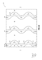
- the spacers along adjacent islands 80 interconnect to form a patterned mask which defines trenches 88 - 90 which serpentine curvilinearly along the second direction of axis 7 .
- FIG. 19 shows that the trenches 88 - 90 extend to an upper surface of semiconductor substrate 8 .
- Locations for the patterned structures 22 , 24 and 26 are defined at bases of the trenches 88 - 90 (with such locations being diagrammatically illustrated utilizing dashed lines).
- the materials 82 and 84 may be together considered to define masking material 92 patterned to have the trenches 88 - 90 extending therethrough.
- the trenches 88 - 90 are extended into semiconductor substrate 8 in the locations where patterned structures 22 , 24 and 26 are to be formed. (In other embodiments, the trenches may not be extended into the substrate, but may instead be utilized to pattern a dopant implant, to pattern conductive material in a damascene process, etc.)
- patterned structures 94 - 96 are formed within the trenches 88 - 90 ( FIGS. 20 and 21 ).
- the patterned structures 94 - 96 may correspond to the structures 22 - 24 in some embodiments.
- the patterned structures 94 - 96 may comprise sacrificial material in the illustrated embodiment. Such sacrificial material may be any suitable material; and in some embodiments may comprise silicon dioxide, silicon nitride, etc.
- the structures 94 - 96 comprise projections 97 extending above an upper surface of semiconductor substrate 8 .
- the patterned structures 94 - 96 may be considered to comprise the segments 30 - 35 described above with reference to FIG. 4 .
- Such segments may be considered to comprise the first set extending along axis 9 (i.e., segments 30 , 32 and 34 ), and the second set extending along axis 11 (segments 31 , 33 and 35 ). All of the segments 30 - 35 are simultaneously formed in the embodiment of FIGS. 17-22 .
- the pattern utilized to form the first set of segments ( 30 , 32 and 34 ) and the pattern utilized to form the second set of segments ( 31 , 33 and 35 ) are provided simultaneously in the embodiment of FIGS.
- FIGS. 24 and 25 are views along the line X-X of FIG. 24 .
- masking material 92 FIGS. 22 and 23 .
- spacer material 98 is formed along the projections 97 of structures 94 - 96 to form spacers 100 .
- the spacers 86 of FIGS. 18 and 19 may be referred to as first spacers
- the spacers 100 of FIGS. 26 and 27 may be referred to as second spacers.
- the spacer material 98 may comprise any suitable composition or combination of compositions; including, for example, one or more of silicon dioxide, silicon nitride, etc.
- the spacers 100 are aligned with the patterned structures 94 - 96 and define trenches 102 - 104 which serpentine curvilinearly along the second direction of axis 7 .
- the trenches 102 - 104 may be referred to as second trenches to distinguish them from the first trenches 88 - 90 of FIGS. 18 and 19 .
- the second trenches 102 - 104 duplicate the first trenches 80 - 90 , and alternate with the first trenches along the direction of axis 5 .
- the trenches 102 - 104 define locations for patterned structures 23 , 25 and 27 ; with such locations being diagrammatically illustrated in FIG. 27 utilizing dashed lines.
- FIGS. 28 and 29 (with FIG. 29 being a view along the line X-X of FIG. 28 ), the trenches 102 - 104 are extended into semiconductor substrate 8 in the locations where patterned structures 23 , 25 and 27 are to be formed.
- FIGS. 30 and 31 are views along the line X-X of FIG. 30 .
- patterned structures 94 - 96 FIGS. 28 and 29
- spacer material 98 FIGS. 28 and 29
- trenches 88 , 102 , 89 , 103 , 90 and 104 are removed to leave trenches 88 , 102 , 89 , 103 , 90 and 104 defining locations where patterned structures 22 - 27 are to be formed.
- the structures 94 - 96 of FIGS. 28 and 29 were temporary patterned structures formed within the first trenches 88 - 90 in order to align the second trenches 102 - 104 with the first trenches.
- such temporary patterned structures may be referred to as first patterned structures.
- the patterned structures 22 - 27 comprise the first set of segments extending along axis 9 (i.e., segments 30 , 32 and 34 ), and the second set of segments extending along axis 11 (segments 31 , 33 and 35 ). All of the segments 30 - 35 are defined by the patterned trenches 88 , 102 , 89 , 103 , 90 and 104 of FIGS. 30 and 31 .
- the trenches 88 , 102 , 89 , 103 , 90 and 104 define locations for patterned structures 22 - 27 .
- Such patterned structures will serpentine curvilinearly across semiconductor substrate 8 in the same manner in which the trenches 88 , 102 , 89 , 103 , 90 and 104 serpentine across the substrate.
- example conductive structures 22 - 27 are formed within trenches 88 , 102 , 89 , 103 , 90 and 104 .
- the conductive structures comprise conductive material 106 .
- Such conductive material may be any suitable conductive material, including, for example, one or more of conductively-doped semiconductor material, metal, and metal-containing compositions.
- the conductive material 106 is shown to be spaced from semiconductor substrate 8 by insulative material 108 .
- Such insulative material may comprise any suitable composition or combination of compositions; including, for example, one or both of silicon dioxide and silicon nitride.
- the upper region of semiconductor substrate 8 is electrically insulative, and accordingly the insulative material 108 may be omitted.
- semiconductor substrate 8 comprises semiconductor material exposed at the bottoms of trenches 88 , 102 , 89 , 103 , 90 and 104 ; and conductive regions 106 correspond to conductively-doped regions of the semiconductor material.
- the patterned structures 94 - 96 are temporary structures utilized to align the second trenches 102 - 104 ( FIGS. 26 and 27 ) with the first trenches 88 - 90 ( FIGS. 18 and 19 ).
- the second trenches 102 - 104 are formed with identical processing as is utilized to form the first trenches 88 - 90 (i.e., islands and spacers analogous to the islands 80 and spacers 86 of FIG. 18 ), and after formation of the first trenches 88 - 90 .
- the temporary patterned structures 94 - 96 may be omitted and instead replaced with conductive structures (e.g., structures comprising conductive material 106 ).
- the structures 22 - 27 may correspond to digit lines in the illustrated embodiment. In other embodiments the structures 22 - 27 may correspond to other integrated circuitry in addition to, or alternatively to, digit lines.
- the structures 22 - 27 of FIG. 33 are generically illustrated, and may be utilized in any suitable application.
- the structures 22 - 27 may correspond to digit lines, and may be utilized in DRAM arrays, in arrays comprising ferroelectric memory, etc.
- a specific example of a memory array configuration is described with reference to a memory array 200 in FIG. 34 .
- the memory array 200 comprises fin field effect transistors (finFETs) 202 - 207 , with each finFET including a fin 208 of semiconductor material 210 .
- the fins include pedestals 212 and 214 , with such pedestals joining through a trough 216 .
- Each of the pedestals 212 and 214 may comprise source/drain regions 213 and 215 , respectively.
- a channel region 217 extends around the trough 216 and between the source/drain regions 213 and 215 .
- a wordline 218 is diagrammatically illustrated with dashed-lines, as the wordline is out of the plane of the view of FIG. 34 (and specifically is in front of such plane).
- the wordline may comprise gates of the finFETs 202 - 207 , with such gates being spaced from the semiconductor material 210 by gate dielectric (not shown). In operation, the gates control current flow along the channel regions 217 .
- the fins 208 are spaced from one another by dielectric material 220 .
- the dielectric material 220 also extends within the troughs 216 .
- Capacitors 222 are electrically coupled with the source/drain regions 213 , and the structures 22 - 27 are digit lines electrically coupled with the source/drain regions 215 .
- the capacitors 222 may be non-ferroelectric and/or may be ferroelectric capacitors.
- the capacitors 222 , digit lines (structures 22 - 27 ) and finFETs 202 - 207 are together incorporated into the memory array 200 , with such memory array having memory cells which store data as a charge state of the capacitors.
- Such electronic systems may be used in, for example, memory modules, device drivers, power modules, communication modems, processor modules, and application-specific modules, and may include multilayer, multichip modules.
- the electronic systems may be any of a broad range of systems, such as, for example, cameras, wireless devices, displays, chip sets, set top boxes, games, lighting, vehicles, clocks, televisions, cell phones, personal computers, automobiles, industrial control systems, aircraft, etc.
- the various materials, substances, compositions, etc. described herein may be formed with any suitable methodologies, either now known or yet to be developed, including, for example, atomic layer deposition (ALD), chemical vapor deposition (CVD), physical vapor deposition (PVD), etc.
- ALD atomic layer deposition
- CVD chemical vapor deposition
- PVD physical vapor deposition
- dielectric dielectric
- electrically insulative dielectrically insulative
- the terms are considered synonymous in this disclosure.
- the utilization of the term “dielectric” in some instances, and the term “electrically insulative” in other instances, may be to provide language variation within this disclosure to simplify antecedent basis within the claims that follow, and is not utilized to indicate any significant chemical or electrical differences.
- Some embodiments include a method of forming a pattern.
- a semiconductor substrate is provided to have rows extending along a first direction. The rows are spaced from one another along a second direction. Each of the rows includes course regions that are to be included along patterned structures which extend generally along the second direction. The rows are subdivided amongst first and second rows which alternate with one another along the second direction. The course regions within the first rows are staggered relative to the course regions within the second rows.
- the patterned structures comprise first segments which extend along a third direction intermediate the first and second directions, and comprise second segments which extend along a fourth direction intermediate the first and second directions and which is different from the third direction.
- Patterned masking material is formed across the semiconductor substrate to define a first pattern comprising the first segments of the patterned structures, and to define a second pattern comprising the second segments of the patterned structures.
- the patterned structures are formed within the first and second patterns defined by the patterned masking material.
- Some embodiments include a method of forming a pattern.
- a semiconductor substrate is provided to have rows extending along a first direction. The rows are spaced from one another along a second direction. Each row comprises course regions that are to be included along patterned structures extending generally along the second direction. The rows are subdivided amongst first and second rows which alternate with one another along the second direction. The course regions within the first rows are staggered relative to the course regions within the second rows. Islands of masking material are formed over alternating course regions along the rows. Spacers are formed along lateral peripheries of the islands. The spacers along adjacent islands interconnect to form a patterned mask which defines trenches that serpentine curvilinearly along the second direction. The patterned structures are formed within the trenches.
- Some embodiments include a method of forming a pattern.
- a semiconductor substrate is provided to have rows extending along a first direction. The rows are spaced from one another along a second direction. Each row comprises alternating first regions and second regions. The first regions are course regions that are to be included along patterned structures extending generally along the second direction. The rows are subdivided amongst first and second rows which alternate with one another along the second direction. The course regions within the first rows are staggered relative to the course regions within the second rows. Blocking material segments are formed along the rows. The blocking material segments are across every other space between first and second regions along the rows. A first patterned mask is formed across the semiconductor substrate and the blocking material segments.
- the first patterned mask defines a plurality of substantially linear first trenches which extend along a third direction intermediate the first and second directions. First segments of the patterned structures are formed within the first trenches. A second patterned mask is formed across the semiconductor substrate, across the blocking material segments, and across the first segments of the patterned structures. The second pattern patterned mask defines a plurality of substantially linear second trenches which extend along a fourth direction intermediate the first and second directions, and which is different from the third direction. Second segments of the patterned structures are formed within the second trenches. The first and second segments of the patterned structures connect with one another to form the patterned structures. Each of the patterned structures extends in a zigzag manner across the first and rows along the second direction.
- Some embodiments include an apparatus comprising a plurality of finFETs arranged in line in a first direction and a digit line formed in a zigzag pattern.
- Each of the plurality of finFETs comprises a first pedestal serving as a first source/drain region, a second pedestal serving as a second source/drain region and a trough defining a channel region between the first and second source/drain regions.
- the first and second source/drain regions of each of the plurality of finFETs are disposed in line in a second direction that is substantially perpendicular to the first direction.
- An arrangement in the second direction of the first and second source/drain region of each of even-numbered ones of the plurality of finFETs is reverse to an arrangement in the second direction of the first and second source/drain regions of each of odd-numbered ones of the plurality of finFETs such that the first source/drain region of each of the even-numbered ones of the plurality of finFETs is sandwiched in the first direction between the second source/drain regions of corresponding adjacent two of odd-numbered ones of the plurality of finFETs.
- the digit line is formed in a zigzag pattern to electrically interconnect the first source/drain regions of the plurality of finFETs to each other.
- Some embodiments include an apparatus comprising a plurality of finFETs arranged in matrix including a plurality of rows and a plurality of columns and a plurality of digit lines.
- Each of the plurality of finFETs comprises a first pedestal serving as a first source/drain region, a second pedestal serving as a second source/drain region and a trough defining a channel region between the first and second source/drain regions.
- the first and second source/drain regions of each of the plurality of finFETs are disposed in a row direction.
- Each of even-numbered ones of the plurality of rows are shifted in a row direction with respect to each of odd-numbered ones of the plurality of rows such that the first source/drain region of each of the plurality of finFETs belonging to each of the even-numbered ones of the plurality of rows is sandwiched in a column direction between the second source/drain regions of corresponding adjacent two of the plurality of finFETs belonging to each of the odd-numbered ones of the plurality of rows.
- Each of the plurality of digit lines is formed in a zigzag pattern to electrically interconnect the first source/drain regions of the plurality of finFETs belonging to a corresponding one of the plurality of columns.
Landscapes
- Engineering & Computer Science (AREA)
- Chemical & Material Sciences (AREA)
- Inorganic Chemistry (AREA)
- Physics & Mathematics (AREA)
- Condensed Matter Physics & Semiconductors (AREA)
- General Physics & Mathematics (AREA)
- Manufacturing & Machinery (AREA)
- Computer Hardware Design (AREA)
- Microelectronics & Electronic Packaging (AREA)
- Power Engineering (AREA)
- Internal Circuitry In Semiconductor Integrated Circuit Devices (AREA)
Abstract
Description
Claims (20)
Priority Applications (1)
| Application Number | Priority Date | Filing Date | Title |
|---|---|---|---|
| US15/391,405 US9853027B1 (en) | 2016-12-27 | 2016-12-27 | Methods of forming patterns, and apparatuses comprising FinFETs |
Applications Claiming Priority (1)
| Application Number | Priority Date | Filing Date | Title |
|---|---|---|---|
| US15/391,405 US9853027B1 (en) | 2016-12-27 | 2016-12-27 | Methods of forming patterns, and apparatuses comprising FinFETs |
Publications (1)
| Publication Number | Publication Date |
|---|---|
| US9853027B1 true US9853027B1 (en) | 2017-12-26 |
Family
ID=60674418
Family Applications (1)
| Application Number | Title | Priority Date | Filing Date |
|---|---|---|---|
| US15/391,405 Active US9853027B1 (en) | 2016-12-27 | 2016-12-27 | Methods of forming patterns, and apparatuses comprising FinFETs |
Country Status (1)
| Country | Link |
|---|---|
| US (1) | US9853027B1 (en) |
Cited By (2)
| Publication number | Priority date | Publication date | Assignee | Title |
|---|---|---|---|---|
| US20200152571A1 (en) * | 2017-08-29 | 2020-05-14 | Micron Technology, Inc. | Integrated Assemblies |
| US10692887B2 (en) | 2017-08-29 | 2020-06-23 | Micron Technology, Inc. | Methods used in forming an array of memory cells |
Citations (5)
| Publication number | Priority date | Publication date | Assignee | Title |
|---|---|---|---|---|
| US20090237996A1 (en) | 2008-03-20 | 2009-09-24 | Micron Technology, Inc. | Memory structure having volatile and non-volatile memory portions |
| US20110193157A1 (en) | 2010-02-08 | 2011-08-11 | Micron Technology, Inc. | Cross-hair cell based floating body device |
| US8741758B2 (en) | 2010-02-09 | 2014-06-03 | Micron Technologies, Inc. | Cross-hair cell wordline formation |
| US20140185355A1 (en) | 2008-03-20 | 2014-07-03 | Micron Technology, Inc. | Systems and Devices Including Multi-Transistor Cells and Methods of Using, Making, and Operating the Same |
| US20140374809A1 (en) * | 2013-06-20 | 2014-12-25 | Je-min Park | Pads including curved sides and related electronic devices, structures, and methods |
-
2016
- 2016-12-27 US US15/391,405 patent/US9853027B1/en active Active
Patent Citations (5)
| Publication number | Priority date | Publication date | Assignee | Title |
|---|---|---|---|---|
| US20090237996A1 (en) | 2008-03-20 | 2009-09-24 | Micron Technology, Inc. | Memory structure having volatile and non-volatile memory portions |
| US20140185355A1 (en) | 2008-03-20 | 2014-07-03 | Micron Technology, Inc. | Systems and Devices Including Multi-Transistor Cells and Methods of Using, Making, and Operating the Same |
| US20110193157A1 (en) | 2010-02-08 | 2011-08-11 | Micron Technology, Inc. | Cross-hair cell based floating body device |
| US8741758B2 (en) | 2010-02-09 | 2014-06-03 | Micron Technologies, Inc. | Cross-hair cell wordline formation |
| US20140374809A1 (en) * | 2013-06-20 | 2014-12-25 | Je-min Park | Pads including curved sides and related electronic devices, structures, and methods |
Cited By (4)
| Publication number | Priority date | Publication date | Assignee | Title |
|---|---|---|---|---|
| US20200152571A1 (en) * | 2017-08-29 | 2020-05-14 | Micron Technology, Inc. | Integrated Assemblies |
| US10692887B2 (en) | 2017-08-29 | 2020-06-23 | Micron Technology, Inc. | Methods used in forming an array of memory cells |
| US10978484B2 (en) | 2017-08-29 | 2021-04-13 | Micron Technology, Inc. | Methods used in forming an array of memory cells |
| US11348871B2 (en) * | 2017-08-29 | 2022-05-31 | Micron Technology, Inc. | Integrated assemblies |
Similar Documents
| Publication | Publication Date | Title |
|---|---|---|
| US12295143B2 (en) | Methods for forming multilayer horizontal NOR-type thin-film memory strings | |
| US11062989B2 (en) | Assemblies which include wordlines over gate electrodes | |
| CN112185961B (en) | Integrated assembly and method of forming an integrated assembly | |
| US8274112B2 (en) | Semiconductor memory device having pillar structures | |
| CN101297392B (en) | Silicided recessed silicon | |
| US9245893B1 (en) | Semiconductor constructions having grooves dividing active regions | |
| US8518812B2 (en) | Methods of forming electrical contacts | |
| US6518124B1 (en) | Method of fabricating semiconductor device | |
| US9613967B1 (en) | Memory device and method of fabricating the same | |
| US8415738B2 (en) | Semiconductor memory device and manufacturing method thereof | |
| TW201635493A (en) | Double-turn static random access memory cell structure with vertical components and manufacturing method thereof | |
| US9875960B1 (en) | Memory arrays | |
| KR20170100669A (en) | Method for forming self-aligned discrete gate memory cell arrays with metal gates and logic devices | |
| US11888068B2 (en) | Integrated transistors having gate material passing through a pillar of semiconductor material, and methods of forming integrated transistors | |
| CN115312520A (en) | Integrated assembly and method of forming an integrated assembly | |
| TW201631706A (en) | Memory device and method of fabricating the same | |
| US12225707B2 (en) | Method for manufacturing semiconductor structure, semiconductor structure and semiconductor memory | |
| TW202114159A (en) | Self-aligned contacts for 3d logic and memory | |
| US9853027B1 (en) | Methods of forming patterns, and apparatuses comprising FinFETs | |
| US9646875B2 (en) | Methods of forming memory arrays | |
| US20250311205A1 (en) | Semiconductor structure and method of forming the same | |
| US20180182765A1 (en) | Methods of Forming Memory Arrays | |
| JP2013008768A (en) | Semiconductor device and manufacturing method of the same | |
| JP7302024B2 (en) | Local wordline driver device, memory device, and method of manufacture | |
| US8207041B2 (en) | Semiconductor processing methods |
Legal Events
| Date | Code | Title | Description |
|---|---|---|---|
| AS | Assignment |
Owner name: MICRON TECHNOLOGY, INC., IDAHO Free format text: ASSIGNMENT OF ASSIGNORS INTEREST;ASSIGNOR:JUENGLING, WERNER;REEL/FRAME:040775/0796 Effective date: 20161222 |
|
| AS | Assignment |
Owner name: MORGAN STANLEY SENIOR FUNDING, INC., MARYLAND Free format text: SUPPLEMENT NO. 3 TO PATENT SECURITY AGREEMENT;ASSIGNOR:MICRON TECHNOLOGY, INC.;REEL/FRAME:041675/0105 Effective date: 20170124 |
|
| STCF | Information on status: patent grant |
Free format text: PATENTED CASE |
|
| AS | Assignment |
Owner name: JPMORGAN CHASE BANK, N.A., AS COLLATERAL AGENT, ILLINOIS Free format text: SECURITY INTEREST;ASSIGNORS:MICRON TECHNOLOGY, INC.;MICRON SEMICONDUCTOR PRODUCTS, INC.;REEL/FRAME:047540/0001 Effective date: 20180703 Owner name: JPMORGAN CHASE BANK, N.A., AS COLLATERAL AGENT, IL Free format text: SECURITY INTEREST;ASSIGNORS:MICRON TECHNOLOGY, INC.;MICRON SEMICONDUCTOR PRODUCTS, INC.;REEL/FRAME:047540/0001 Effective date: 20180703 |
|
| AS | Assignment |
Owner name: MICRON TECHNOLOGY, INC., IDAHO Free format text: RELEASE BY SECURED PARTY;ASSIGNOR:MORGAN STANLEY SENIOR FUNDING, INC., AS COLLATERAL AGENT;REEL/FRAME:050695/0825 Effective date: 20190731 |
|
| AS | Assignment |
Owner name: MICRON TECHNOLOGY, INC., IDAHO Free format text: RELEASE BY SECURED PARTY;ASSIGNOR:JPMORGAN CHASE BANK, N.A., AS COLLATERAL AGENT;REEL/FRAME:051028/0001 Effective date: 20190731 Owner name: MICRON SEMICONDUCTOR PRODUCTS, INC., IDAHO Free format text: RELEASE BY SECURED PARTY;ASSIGNOR:JPMORGAN CHASE BANK, N.A., AS COLLATERAL AGENT;REEL/FRAME:051028/0001 Effective date: 20190731 |
|
| MAFP | Maintenance fee payment |
Free format text: PAYMENT OF MAINTENANCE FEE, 4TH YEAR, LARGE ENTITY (ORIGINAL EVENT CODE: M1551); ENTITY STATUS OF PATENT OWNER: LARGE ENTITY Year of fee payment: 4 |
|
| MAFP | Maintenance fee payment |
Free format text: PAYMENT OF MAINTENANCE FEE, 8TH YEAR, LARGE ENTITY (ORIGINAL EVENT CODE: M1552); ENTITY STATUS OF PATENT OWNER: LARGE ENTITY Year of fee payment: 8 |