US9852257B1 - Method and system for designing a semiconductor chip based on grouping of hierarchial pins that permit communication between internal components of the semiconductor chip - Google Patents
Method and system for designing a semiconductor chip based on grouping of hierarchial pins that permit communication between internal components of the semiconductor chip Download PDFInfo
- Publication number
- US9852257B1 US9852257B1 US14/692,561 US201514692561A US9852257B1 US 9852257 B1 US9852257 B1 US 9852257B1 US 201514692561 A US201514692561 A US 201514692561A US 9852257 B1 US9852257 B1 US 9852257B1
- Authority
- US
- United States
- Prior art keywords
- pins
- groups
- node
- tree
- chip
- Prior art date
- Legal status (The legal status is an assumption and is not a legal conclusion. Google has not performed a legal analysis and makes no representation as to the accuracy of the status listed.)
- Expired - Fee Related, expires
Links
Images


Classifications
-
- G—PHYSICS
- G06—COMPUTING OR CALCULATING; COUNTING
- G06F—ELECTRIC DIGITAL DATA PROCESSING
- G06F30/00—Computer-aided design [CAD]
- G06F30/30—Circuit design
- G06F30/39—Circuit design at the physical level
- G06F30/392—Floor-planning or layout, e.g. partitioning or placement
-
- G06F17/5077—
-
- G—PHYSICS
- G06—COMPUTING OR CALCULATING; COUNTING
- G06F—ELECTRIC DIGITAL DATA PROCESSING
- G06F30/00—Computer-aided design [CAD]
- G06F30/30—Circuit design
- G06F30/39—Circuit design at the physical level
- G06F30/394—Routing
-
- G—PHYSICS
- G06—COMPUTING OR CALCULATING; COUNTING
- G06F—ELECTRIC DIGITAL DATA PROCESSING
- G06F2113/00—Details relating to the application field
- G06F2113/20—Packaging, e.g. boxes or containers
Definitions
- Embodiments of the present disclosure relate to circuit design, and in particular to circuit design based on a grouping of hierarchical pins that permit communication between internal components and partitions of a chip.
- Chip Designing a complex semiconductor chip (referred to herein generally as “chip”) is usually a time consuming process, and requires several iterations.
- a chip usually has thousands of internal pins for communication between various internal components and partitions of the chip.
- the pins for example, are designed to be placed at specific locations in the chip.
- subsequent modification in the design of the chip typically necessitates a re-design in the placement of the pins.
- Such iterations in the design of the chip are labor intensive and time consuming.
- the present disclosure provides a computer implemented method comprising: while designing a chip, identifying a plurality of partitions in the chip, for a first partition of the plurality of partitions in the chip, identifying a plurality of pins configured to interconnect the first partition with one or more other partitions of the plurality of partitions of the chip, assigning a name to each of the plurality of pins associated with the first partition of the plurality of partitions, based on the names assigned to each of the plurality of pins, forming a plurality of groups such that each group of the plurality of groups is associated with a corresponding one or more pins of the plurality of pins, and based on forming the plurality of groups, designing a first subset of the plurality of pins to be located at close proximity in the chip.
- the present disclosure also provides an apparatus for designing a chip, the apparatus comprising: one or more processors; and a non-transitory computer-readable storage media, wherein instructions are tangibly stored on the computer-readable storage media, wherein the instructions are executable by the one or more processors to enable the one or more processors to design a chip by identifying a plurality of partitions in the chip, for a first partition of the plurality of partitions in the chip, identifying a plurality of pins configured to interconnect the first partition with one or more other partitions of the plurality of partitions of the chip, assigning a name to each of the plurality of pins associated with the first partition of the plurality of partitions, based on the names assigned to each of the plurality of pins, forming a plurality of groups such that each group of the plurality of groups is associated with a corresponding one or more pins of the plurality of pins, and based on forming the plurality of groups, designing a first subset of the plurality of pin
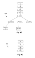
- FIG. 1 schematically illustrates a semiconductor chip divided in a plurality of partitions.
- FIG. 2 illustrates an example formation of a group of pins (referred to herein as “pin groups”) from a plurality of pins, while designing the semiconductor chip of FIG. 1 .
- FIG. 3 illustrates an example of a tree structure that is generated based on prefixes of a plurality of pins.
- FIG. 4 illustrates an example of a tree structure that is generated based on post-fixes of a plurality of pins.
- FIG. 5 illustrates an example of a forest comprising a plurality of tree structures.
- FIG. 6 is a flow diagram of an example method for designing a semiconductor chip.
- FIG. 7 lists a plurality of pins of a semiconductor chip.
- FIGS. 8A-8C illustrate example trees structures, which are formed based on prefixes of various pins.
- FIGS. 8D-8E illustrate example trees structures, which are formed based on post-fixes of various pins.
- FIGS. 9A-9E illustrate trees structures generated from the trees structures of FIGS. 8A-8E , respectively.
- FIGS. 10A-10E illustrate trees structures generated from the trees structures of FIGS. 9A-9E , respectively.
- FIG. 11 is a flow diagram of another example method for designing a semiconductor chip.
- FIG. 1 schematically illustrates a semiconductor chip 100 (henceforth referred to as “chip 100 ”).
- the chip 100 for example, comprises a system on a chip (SOC).
- the chip 100 is partitioned in a plurality of partitions 104 a , . . . , 104 h .
- FIG. 1 illustrates a specific number, specific shapes and specific sizes of the partitions, the chip 100 can have any different number, shapes and/or sizes of the partitions.
- the partitions 104 a , . . . , 104 h partitions or divides the chip 100 in different functional or logical areas.
- the partition 104 a represents a processing core of the chip 104 a
- the partition 104 b represents a level 1 (L1) cache of the chip, and so on.
- a partition of the chip 100 communicates with one or more other partitions of the chip 100 via a corresponding plurality of pins.
- Three example pins 108 are illustrated in FIG. 1 , which facilitate communication between the partition 104 a and the partition 104 d . Although only three example pins are illustrated in FIG. 1 , the chip 100 can comprise hundreds, and even thousands of such pins.
- the pins are used for intra-partition communication, e.g., communication between two partitions of the chip 100 .
- a pin is, for example, a connector that communicates signals between two corresponding partitions.
- a pin refers to a single connector, a single wire or a single communication link (e.g., comprising a single bit communication link) that carries signals.
- a bus refers to a group of pins.
- a port refers to a group of buses.
- An Advanced eXtensible Interface (AXI) is an example of a port.
- An Advanced Microcontroller Bus Architecture (AMBA) High-performance Bus (AHB) is another example of a port.
- a port of the chip 100 comprises a plurality of pins.
- the design of the chip 100 is an iterative and time consuming process. For example, while designing the chip 100 , various partitions and the pins associated with the partitions are designed. Any change in the partition design also changes the layout, design and/or number of the pins. Furthermore, the number of pins present in a typical chip usually ranges in thousands, which makes the design and placement of the pins during the designing of the chip 100 even more challenging. As discussed herein later in more detail, to better stream-line the design of the chip, in an embodiment, the pins associated with a specific partition are assigned respective names (e.g., based on the functionality of the pins). The pins are then grouped in two or more pin groups based on the assigned names, and during an iteration of the design, multiple pins are designed to be placed in close proximity in the chip based on the groupings of the pins.
- respective names e.g., based on the functionality of the pins
- the pins that are to be included within the chip 100 are assigned respective names.
- the naming of a pin is, for example, based on a functionality of the pin, a port in which the pin is to be included, a partition with which the pin is to be associated, a partition to which signals via the pin are to be transmitted, a combination of these factors, and/or the like.
- standard naming conventions, protocols or rules are followed while naming the pins, and the standard naming conventions, protocols or rules are known to those who are designing the chip 100 .
- the same standard naming conventions, protocols or rules are followed in naming each of the pins (or at least most of the pins) of the chip 100 .
- the partition 104 a communicates with the partition 104 e , and in such a communication, the partition 104 a is a master and the partition 104 e is a slave. Also, assume that the partition 104 a is transmitting write data to the partition 104 e . Accordingly, a pin in the partition 104 a , which transmits write data from the partition 104 a to the partition 104 e , is named as mstr5_wdata.
- the partition 104 a is master to the partition 104 e , and is transmitting write data to the partition 104 e —the number “5” identifies the partition 104 e , to which the write data is being transmitted; the phrase “mstr” denotes master; and the phrase “wdata” denotes write data.
- the name of the pin mstr5_wdata is based on a functionality of the pin, and also based on a destination of the signal transmitted via the pin.
- FIG. 2 illustrates formation of pin groups from a plurality of pins, while designing the chip 100 .
- FIG. 2 comprises three columns.
- the first column in FIG. 2 (labeled as column 1 in FIG. 2 ) comprises names of pins that are associated with a specific partition of the chip, e.g., the partition 104 a .
- the partition 104 a can be associated with hundreds, and perhaps thousands of pins, only some of the pin names are illustrated in the first column of FIG. 2 for purposes of simplicity and to not obscure the inventive principles of this disclosure.
- some of the pin names include in parenthesis a specific number.
- the first two pins in the first column are mstr5_wdata[0] and mstr5_wdata[1], implying that a bus mstr5_wdata comprises two signals that are transmitted over the two associated pins.
- the second column in FIG. 2 illustrates different bus groups.
- the pins mstr5_wdata[0] and mstr5_wdata[1] form a bus mstr5_wdata.
- the first bus in FIG. 2 is mstr5_wdata, which comprises signals from the two associated pins mstr5_wdata[0] and mstr5_wdata[1].
- the pins mstr5_wid[0] and mstr5_wid[1] form a bus mstr5_wid, as illustrated in FIG. 2 .
- bus aRReadyCxbar in the second column of FIG. 2 comprises a single pin of the same name.
- some of the bus names comprise an asterisk sign (“*”) at the end.
- the bus mstr5_wdata* comprises the asterisk sign at the end.
- the asterisk sign implies one or more wild characters (e.g., which can be any appropriate characters).
- the name of the bus mstr5_wdata* indicates that the bus comprises pins with names that start with “mstr5wdata” and have one or more other characters at the end. Accordingly, the pins mstr5_wdata[0] and mstr5_wdata[1] are included in the bus mstr5_wdata*.
- pin groups are formed from the bus groups.
- a pin group comprises one or more bus groups.
- the third column of FIG. 2 illustrates the pin groups.
- the pin groups are formed based on prefixes or post-fixes (e.g., suffixes) of the names of the bus groups. For example, bus groups that have similar prefixes (e.g., same starting characters in their respective names) are grouped in a corresponding pin group. In another example, bus groups that have similar post-fixes (e.g., same ending characters in their respective names) are grouped in a corresponding pin group.
- prefixes or post-fixes e.g., suffixes
- the second column comprises bus groups that are named mstr5_wdata*, mstr5_wid* and mstr5_wvalid.
- these three bus groups have the same prefix mstr5_
- these three bus groups are grouped within a pin group named mstr5_*.
- the asterisk sign at the end of the pin group mstr5_* indicates that this pin group includes bus groups that start with mstr5 — and have one or more other characters at the end.
- the second column comprises bus groups that are named rDataCxbar*, rldCxbar*, aRReadyCxbar and aRValidCxbar.
- these four bus groups have the same post-fix Cxbar, these four bus groups are grouped within a pin group named *Cxbar.
- the asterisk sign at the beginning of the pin group Cxbar indicates that this pin group includes bus groups that end with Cxbar and have one or more other characters at the beginning.
- one or more of the pins and bus groups in FIG. 2 are associated with testing the corresponding partition.
- the bus groups associated with testing are grouped under a pin group named Jtag (Joint Test Action Group), although for example, any other appropriate name (e.g., test pin group, testing, etc.) can also be used instead.
- Jtag Joint Test Action Group
- Such grouping of the bus groups in addition to or instead of being based on prefixes and post-fixes of the names, is based on functionality of the pins of the bus groups.
- bus groups are included, for example, in a miscellaneous pin group (labeled as “misc” in FIG. 2 ).
- a partition of a chip can have as many as 3600 pins. In an example, these 3600 pins are reduced to 242 bus groups. The 242 bus groups are further reduced to 16 pin groups. Thus, grouping the pins of a partition in pin groups, as illustrated in FIG. 2 , significantly reduces a number of components (e.g., pin groups) that are to be considered while designing the chip 100 .
- FIG. 3 illustrates an example of a tree 300 , based on prefixes of various pins. As the tree 300 is based on prefixes of the corresponding pins, the tree 300 is also referred to as a prefix tree.
- the tree 300 has various nodes placed at various hierarchical levels.
- a parent node of the tree 300 can have one or more children node.
- the parent node is assumed to be at a higher level compared to a child node. Some of the nodes of the tree 300 do not have a corresponding child node.
- the tree 300 is generated from a list of the pins that correspond to a specific partition of the chip 100 . As an example, the tree 300 is generated from the list of the pins that correspond to the partition 104 a of the chip 100 .
- the tree 300 of FIG. 3 is based on the pin groups illustrated in FIG. 2 .
- the top level or the highest level of the tree 300 has a node mstr, which has three child nodes—mstr5, mstr6 and mstr7.
- mstr5_*, mstr6_* and mstr7_* are three pin groups, and the tree 300 is based on these three pin groups.
- the children (and grandchildren, and subsequent generation) of the nodes mstr6 and mstr7 are not illustrated in FIG. 3 . That is, sub-trees underneath the nodes mstr6 and mstr7 are not illustrated in FIG. 3 . Only the children (and grandchildren, and subsequent generation) of the node mstr5 (i.e., the sub-tree underneath the node mstr5) are illustrated in FIG. 3 .
- the nodes in the tree 300 are arranged in an alphabetical order, e.g., to an extent similar to the manner in which words appear in a dictionary.
- all the entries associated with mstr5 starts with mstr5_. So, for example, once it is identified that pins with prefix mstr5 actually has mstr5 — as their prefix, potential pins with entries mstr5_a* is checked first in the list of pins, followed by potential pins with entries mstr5_b*, and so on. As illustrated in FIG.
- the only bus group that has mstr5_r as a prefix is mstr5_rresp. Accordingly, this bus group is included as a child to the node mstr5_r in the tree 300 .
- the two pins mstr5_rresp[0] and mstr5_rresp[1] are included as being children to the node mstr5_rresp in the tree 300 .
- the node mstr5_w is expanded to include associated children and grandchildren in the tree 300 .
- nodes mstr6 and mstr7 are also expanded in a similar manner to complete the tree 300 .
- the tree 300 of FIG. 3 is a prefix tree, as previously discussed herein.
- a post-fix tree is generated for the pin group that ends with the post-fix *Cxbar (which is a name of a pin group, as illustrated in FIG. 2 ).
- FIG. 4 illustrates an example of a tree 400 , based on post-fixes of the pins.
- the tree of FIG. 4 is generated similar to the generation of the tree 300 of FIG. 3 (although it is to be noted that the tree 300 is based on prefixes of the pin names, while the tree 400 is based on post-fixes of the pin names). Accordingly, a more detailed description of the generation of the tree 400 is omitted herein.
- the tree 300 is specific to the pin groups that start with the prefix mstr. As illustrated in FIG. 2 , there are other pin groups that start with different prefixes, and a tree is generated for each of these prefixes. For example, referring to FIG. 2 , a tree is generated for pins that start with prefix bscan (where bscan* is a name of a pin group), another tree is generated for pins that start with prefix Dro, and so on.
- a forest associated with a partition includes a plurality of trees, examples of which are illustrated in FIGS. 3 and 4 .
- FIG. 5 is an example of a forest 500 comprising three trees (although the trees illustrated in the forest 500 do not match with the trees 300 and 400 of FIGS. 3 and 4 , respectively).
- the forest 500 is a simplified illustration of a forest, and an actual forest associated with a partition of the chip 100 can be more complex and can include a larger number of trees.
- the nodes of the trees in the forest 500 are illustrated using black dots.
- a leaf node refers to a node that does not have a child.
- the nodes mstr5_wvalid and mstr5_rreso[0] does not have any corresponding child node—hence, these nodes are categorized as a leaf node.
- the node mstr5 in FIG. 3 has two children, none of which is a leaf node, implying that the first term (i.e., number of children in the tree, excluding leaf nodes) in equation 1 for this node is two. Furthermore, there are three levels underneath the node mstr 5, implying that the second term (number of levels underneath the node in the tree) in equation 1 for this node is 3.
- the third term in equation 1 is “number of similar sub-trees found in the forest”. To determine the value of this term for the node mstr5, the sub-tree underneath the node mstr5 is evaluated, in which the nodes underneath the node mstr5 is considered—however, during such consideration, the prefix mstr5 is ignored. For example, the node mstr 5 has a first child and a second child—(i) the first child has one child and (ii) the second child has three more children, and so on.
- the first child of the node mstr5 is “_r” (i.e., after ignoring the prefix mstr5 from the name of the first child), and the second child of the node mstr5 is “_w”.
- the node_r has a child_rresp
- the node_w has children_wdata, _wid and _wvalid, each of which has corresponding child(ren).
- each of the sub-trees underneath the nodes mstr6 and mstr7 also has a structure and node names that are similar to those of the sub-tree underneath the node mstr5.
- the term “number of similar sub-trees found in the forest” of equation 1 is three (one each for nodes mstr5, mstr6 and mstr7, and assuming that there are no other sub-trees in the forest having similar structure and nomenclature).
- the node weight assigned to the node mstr5 is (2 ⁇ 3 ⁇ 3), i.e., 18. Also, assuming that the sub-tree underneath the node mstr (i.e., the top node of the tree 300 ) is unique in the forest, the node weight assigned to the node mstr is 3 ⁇ 4 ⁇ 1, i.e., 12, which is determined in a similar manner.
- equation 1 discloses multiplying three terms to determine the node weight for a node
- the node weight can be determined in any other appropriate manner as well.
- corresponding weighted values of the three terms can be added to determine the node weight for a node.
- the node weights are determined for all the nodes, except for the leaf nodes. Thus, for example, node weights are not determined for the node mstr5_wvalid.
- the tree 300 comprises a plurality of pins (e.g., the leaf nodes of the tree 300 correspond to the actual pins), and the tree 300 is a prefix tree (i.e., generated based on the prefix mstr being included in each of the pins).
- the pins of the prefix tree 300 are also used to generate one or more post-fix trees (e.g., similar to the post-fix tree 400 of FIG. 4 ).
- the tree 300 comprises pins mstr5_rresp[0], mstr5_rresp[1], mstr6_rresp[0], mstr6_rresp[1], mstr7_rresp[0] and mstr7_rresp[1] (although some of these pins are not illustrated in FIG. 3 for purposes of simplicity), and these pins are used to generate a post-fix tree. Subsequently, the node weights of each node (except for the leaf nodes) of the post-fix trees are determined. Subsequently, node weights of the nodes in the prefix tree 300 and the node weights of the corresponding post-fix trees are compared. The nodes having the highest node weights are selected.
- a node with the highest node weight is selected. For example, as previously discussed herein, the node weight assigned to the node mstr5 in the prefix tree 300 is 18, and the node weight assigned to the node mstr in the prefix tree 300 is 12. Assuming that the node weight assigned to the node mstr5 in the prefix tree 300 is higher than the node weights assigned to the nodes in the corresponding post-fix trees, the node mstr5 is selected.
- the node mstr6 does not fall within the sub-tree beneath the node mstr5 and (ii) the node mstr6 has a node weight that is equal to the node weight of the node mstr5, the node mstr6 is also selected. For similar reasons, the node mstr7 is also selected.
- the pins associated with the selected node is provisionally placed in close proximity (e.g., in a consecutive manner).
- the node mstr5 of the tree 300 is selected.
- the pins mstr5_wdata[0], mstr5_wdata[1], mstr5_wid[0], mstr5_wid[1], mstr5_rresp[0], mstr5_rresp[1] and mstr5_wvalid are associated with the node mstr5.
- the pins mstr5_wdata[0], mstr5_wdata[1], mstr5_wid[0], mstr5_wid[1], mstr5_rresp[0], mstr5_rresp[1] and mstr5_wvalid are to be placed in close proximity (e.g., in consecutive locations, with no other pins being placed in between these pins) in the chip 100 .
- the design (e.g., further iterations of the design) of the chip 100 proceeds. For example, certain space in the chip 100 is reserved for placement of these seven pins associated with the node mstr5.
- one or more nodes from the post-fix tree 400 of FIG. 4 are selected.
- the nodes of the post-fix tree 400 of FIG. 4 are assigned respective node weights (e.g., using equation 1).
- one or more prefix trees corresponding to the post-fix tree 400 are generated, based on the pins included in the post-fix tree 400 .
- the tree 400 has pins aRReadyCxbar and aRValidCxbar.
- a prefix tree is generated using these two pins (e.g., a top node in the prefix tree can be aR*).
- the nodes of the one or more prefix trees are assigned corresponding node weights.
- the node weights of the nodes in the post-fix tree 400 and the corresponding one or more prefix trees are compared, to selected one or more nodes.
- the node Cxbar from the tree 400 is selected. Once the node Cxbar is selected, in the design of the chip 100 , all the pins associated with the selected node Cxbar is provisionally placed in close proximity (e.g., in a consecutive manner).
- FIG. 6 is a flow diagram of an example method 600 for designing a chip (e.g., the chip 100 of FIG. 1 ). The method 600 is performed, for example, while designing the chip.
- a plurality of partitions e.g., partitions 104 , . . . , 104 h
- a plurality of pins e.g., the pins listed in the first column of FIG. 2 for interconnecting the first partition with one or more other partitions of the plurality of partitions of the chip is identified.
- individual pins of the plurality of pins associated with the first partition of the plurality of partitions are named.
- the naming of a pin is, for example, based on a functionality of the pin, a port in which the pin is to be included, a partition with which the pin is to be associated, a partition to which signals via the pin are to be transmitted, a combination of these factors, and/or the like. In an example, standard naming conventions, protocols or rules are followed while naming the pins.
- the plurality of pins is grouped in a plurality of groups of pins, e.g., as illustrated in FIG. 2 .
- a first tree structure (e.g., the tree structure 300 of FIG. 3 ) is generated.
- the first tree structure comprises a first plurality of nodes arranged in hierarchical levels, where the first tree structure is generated based on one of prefixes or post-fixes of the names of the pins included in the first group of pins.
- a corresponding node weight is assigned to each node of the first plurality of nodes of the first tree structure, e.g., as discussed previously herein with respect to equation 1.
- one or more second tree structures are generated. For example, if the first tree structure is generated based on prefixes, the one or more second tree structures are generated based on post-fixes.
- the one or more second tree structures comprise a second plurality of nodes arranged in hierarchical levels. Also at 624 , a corresponding node weight is assigned to each node of the second plurality of nodes of the one or more second tree structures.
- a first node is selected from one of (i) the first tree structure and (ii) the one or more second tree structures. For example, as discussed with respect to FIG. 3 , the node mstr5 is selected.
- a first subset of the plurality of pins is associated with the selected first node. For example, the first subset of the plurality of pins is included in a sub-tree underneath the selected first node.
- the pins of the first subset of the plurality of pins is designed to be located at close proximity (e.g., in consecutive location) in the chip.
- the pins in FIG. 2 were grouped in multiple pin groups, and subsequently tree structures were generated corresponding to the multiple pin groups.
- the pins are initially arranged in form of tree structures, and subsequently, the pins are grouped in multiple groups, as will be discussed in more detail herein below.
- FIG. 7 lists a plurality of pins of the chip 100 .
- the pin names in FIG. 7 correspond to the pin names in the first column of FIG. 2 .
- Assignment of a name to a pin is, for example, based on a functionality of the pin, a port in which the pin is to be included, a partition with which the pin is to be associated, a partition to which signals via the pin are to be transmitted, a combination of these factors, and/or the like, as previously discussed herein.
- FIGS. 8A-8C illustrate example trees 800 a - 800 c , based on prefixes of various pins.
- the trees 800 a - 800 c are also referred to as prefix trees.
- the trees 800 a - 800 c have various nodes placed at various hierarchical levels.
- a parent node of a tree can have one or more children node, one or more grandchildren node, and so on. The parent node is assumed to be at a higher level compared to a child node.
- Some of the nodes of a tree do not have a corresponding child node—these nodes are referred to herein as “leaf nodes”.
- the tree 800 a includes nodes and pins that start with the alphabet “m.”
- the topmost node of the tree 800 a has the alphabet “m.”
- the nodes in the tree 800 a are arranged in an alphabetical order, e.g., to an extent similar to the manner in which words appear in a dictionary. For example, subsequent to forming the topmost node, it is determined whether any pin includes “ma” as a prefix, whether any pin includes “mb” as a prefix, whether any pin includes “mc” as a prefix, and so on. Once it is determined that there are pins that include “ms” as prefix, the second level node is labeled as “ms.” This iterative process continues, thereby forming the tree 800 a of FIG. 8A .
- the children (and grandchildren, and subsequent generation) of the nodes mstr6 and mstr7 are not illustrated in FIG. 8A . That is, sub-trees underneath the nodes mstr6 and mstr7 are not illustrated in FIG. 8A . Only the children (and grandchildren, and subsequent generation) of the node mstr5 (i.e., the sub-tree underneath the node mstr5) are illustrated in FIG. 8A .
- a node in a given level has one additional alphabet compared to the immediate parent level.
- the third level node is “mst,” while the second level node is “ms.”
- mstr5_r which is child to mstr5_r
- mstr5_rre which is child to mstr5_rr
- mstr5_rres which is child to mstr5_rre.
- nodes are not illustrated in FIG. 8 a —instead, the link between the nodes mstr5_r and mstr5_rresp is illustrated using dotted lines to indicate that there are additional nodes present. Similar dotted lines exist between the node mstr5_w and its three children nodes, to indicate presence of nodes not illustrated in FIG. 8A .
- the leaf nodes of FIG. 8A are illustrated using dark/grey shades, to indicate that they are leaf nodes. Usually, the leaf nodes correspond to the actual pins of the chip 100 . For example, the leaf nodes of the tree 800 a are included in the list of pins illustrated in FIG. 7 .
- nodes mstr6 and mstr7 are also expanded in a similar manner to complete the tree 800 a.
- the trees 800 b and 800 c of FIGS. 8B and 8C are generated in a manner that is at least in part similar to the generation of the tree 800 a of FIG. 8A . Accordingly, a more detailed discussion regarding the generation of the trees 800 b and 800 c is omitted herein. It is to be noted that the prefix trees 800 a - 800 c are mere examples, and various other prefix tress covering various other pins of FIG. 7 are also generated.
- FIGS. 8D-8E illustrate example trees 800 d - 800 e , based on post-fixes of various pins. As the trees 800 d - 800 e are based on post-fixes of the corresponding pins, the trees 800 d - 800 e are also referred to as post-fix trees.
- the tree 800 d includes nodes and pins that end with the alphabet “r.”
- the topmost node of the tree 900 has the alphabet “r.”
- the second level node is labeled as “ar.” The iterative process continues, thereby forming the tree 800 d of FIG. 8D .
- a node in a given level has one additional alphabet compared to the immediate parent level. For example, the third level node is “bar,” while the second level node is “ar.”
- nodes of the tree 800 d are omitted for purposes of simplicity.
- the link between the nodes aCxbar and rDataCxbar is illustrated using dotted lines, e.g., to indicate that there are additional nodes present, but not illustrated in the figure.
- the nodes not illustrated in FIG. 8D include node taCxbar (which is a child of the node aCxbar), node ataCxbar (which is a child of the node taCxbar), and so on.
- the leaf nodes of FIG. 8D are illustrated using dark/grey shades, to indicate that they are leaf nodes. Usually, the leaf nodes correspond to the actual pins of the chip 100 . For example, the leaf nodes of the tree 800 d are included in the list of pins illustrated in FIG. 7 .
- the tree 800 e of FIG. 8E is generated in a manner that is at least in part similar to the generation of the tree 800 d of FIG. 8D . Accordingly, a more detailed discussion regarding the generation of the tree 800 e is omitted herein. It is to be noted that the post-fix trees 800 d - 800 e are mere examples, and various other post-fix tress covering various other pins of FIG. 7 are also generated.
- the pin mstr5_wdata[0] is included in the prefix tree 800 a of FIG. 8A and also included in the post-fix tree 800 e of FIG. 8E .
- a pin can be included in a prefix tree and a post-fix tree (although a pin cannot be included in more than one prefix tree, or be included in more than one post-fix tree).
- pins that belong to a miscellaneous category of pins there are pins that belong to a miscellaneous category of pins (identified as “misc” in FIG. 2 ).
- the pins of the miscellaneous category do not necessarily have other pins with the same prefixes or post-fixes.
- a pin of the miscellaneous category may not be included in a prefix tree or a post-fix tree.
- Most pins, which do not belong to the miscellaneous category are included in one prefix tree and one post-fix tree.
- the pin mstr5_wdata[0] is included in the prefix tree 800 a of FIG. 8A and also included in the post-fix tree 800 e of FIG. 8E .
- FIGS. 9A-9C illustrate prefix trees 900 a - 900 c , respectively, which are respectively generated by eliminating the leaf nodes from the prefix trees 800 a - 800 c of FIGS. 8A-8C , respectively.
- the tree 900 a of FIG. 9A is similar to the tree 800 a of FIG. 8A , but with the leaf nodes eliminated from the tree 800 a.
- FIGS. 9D-9E illustrate post-fix trees 900 d - 900 e , respectively, which are respectively generated by eliminating the leaf nodes from the post-fix trees 800 d - 800 e of FIGS. 8D-8E , respectively.
- the post-fix tree 900 d of FIG. 9D is similar to the post-fix tree 800 d of FIG. 8D , but with the leaf nodes eliminated from the post-fix tree 800 d.
- each of the leaf nodes in 8 A- 8 E has a corresponding grand-parent node, and accordingly, the leaf nodes in 8 A- 8 E are eliminated to generate the trees in FIGS. 9A-9E , respectively.
- an interim parent node is merged with a corresponding child node, if the parent node has only one child node.
- FIGS. 10A-10E illustrate trees 1000 a - 1000 e , respectively, which are respectively generated from the trees 900 a - 900 e of FIGS. 9A-9E .
- individual ones of various parent nodes are merged with a corresponding child node, if the parent node has a single child node.
- the node “m” has a single child node ms, which also has a single child node mst, and so on. Accordingly, the node “m” is merged with the corresponding child node ms, which is merged with its single child node mst, and which is again merged with the single child node mstr. Accordingly, the parent, grand-parent and previous generation of the node mstr is merged with the node mstr, as illustrated in FIG. 10A . Thus, in the tree 1000 a of FIG. 10 a , the node mstr does not have any parent node.
- the dotted link between the nodes mstr5_r and mstr5_rresp in the tree 900 a of FIG. 9A indicates presence of several nodes. However, all these nodes are merged to the node mstr5_rresp, as illustrated in the tree 1000 a in FIG. 10A . Accordingly, the link between the nodes mstr5_r and mstr5_rresp in the tree 1000 a in FIG. 10A is no longer dotted, as there are no intervening nodes between these two nodes in the tree 1000 a.
- the trees 1000 b - 1000 e of FIGS. 10B-10E are similarly generated from the trees 900 b - 900 e of FIGS. 9B-9E , respectively.
- each node of the tree 900 c of FIG. 9C has a single corresponding child node
- each node of the tree 900 c is merged to a single node bscan in the tree 1000 c in FIG. 10C .
- the selective merging of a parent node to a corresponding child node is performed both for prefix trees (e.g., as illustrated in FIGS. 10A-10C ) and post-fix trees (e.g., as illustrated in FIGS. 10D-10E ).
- a root node (e.g., the top-most node) can represent an abstraction pin group.
- the root node dro of the tree 1000 b of FIG. 10B represents a possible abstraction pin group.
- a tree can also represent more than one abstraction pin group.
- the tree 1000 a of FIG. 10A comprises three abstraction pin groups—mstr5, mstr6 and mstr7.
- each node of the tree is assigned a node weight.
- the assignment of node weights have been discussed in detail herein earlier.
- the equation 1 previously discussed herein (or a suitable variation of equation 1, as also previously discussed herein) is used to assign node weights to individual nodes of each tree.
- equation 1 has a term (number of children in the tree, excluding leaf nodes).
- the leaf nodes have already been eliminated (e.g., while generating the trees 900 a - 900 e from the trees 800 a - 800 e ).
- the first term of the equation 1 is modified to be (number of children in the tree).
- Node weight of a node of a tree (number of children in the tree) ⁇ (number of levels underneath the node in the tree) ⁇ (number of similar sub-trees found in the forest) Equation 1a
- leaf nodes are not removed from the trees 1000 a - 1000 e , and the original equation 1 is used instead to generate node weights.
- equation 1a is applied to determine the node weights of various nodes of the tree 1000 a of FIG. 10A .
- the node weight assigned to the node mstr of the tree 1000 a of FIG. 10A is 3*4*1, i.e., 12.
- the node weight assigned to the node mstr5 of the tree 1000 a of FIG. 10A is 2*3*3, i.e., 18.
- 10A is also assigned the same node weight of 18. Accordingly, as the node weights assigned to the nodes mstr5, mstr6 and mstr7 are equal and are highest among all the node weights assigned to all the nodes of the tree 1000 a , the nodes mstr5, mstr6 and mstr7 are selected to represent abstract pin groups for the tree 1000 a.
- the nodes dro, bscan, Csbar and data of the trees 1000 b - 1000 e are selected to represent abstract pin groups of the respective trees.
- each abstract pin groups has a corresponding root node.
- the nodes mstr5, mstr6, mstr7, dro, bscan, Cxbar and data of the trees 1000 a - 1000 e form corresponding abstract pin groups.
- each abstract pin group has a corresponding intrinsic pin coverage.
- the abstract pin group mstr5 covers pins mstr5_wdata[0], mstr5_wdata[1], mstr5_wid[0], mstr5_wid[1], mstr5_rresp[0], mstr5_rresp[1] and mstr5_wvalid.
- FIG. 8A the abstract pin group mstr5 covers pins mstr5_wdata[0], mstr5_wdata[1], mstr5_wid[0], mstr5_wid[1], mstr5_rresp[0], mstr5_rresp[1] and mstr5_wvalid.
- the abstract pin group dro covers pins droClkOut_fm_cpuSS, droClkOut_to_cpuSS, droEnOut_fm_cpuSS and droEnOut_to_cpuSS.
- a number of pins covered by an abstract pin group is referred to as an intrinsic coverage of the abstract pin group.
- the intrinsic coverage of the abstract pin group mstr5 is seven.
- the intrinsic coverage of the abstract pin group dro is four.
- each abstract pin group is classified as a prefix abstract pin group or a post-fix abstract pin group, based on a tree from which the abstract pin group is derived. Accordingly, the abstract pin groups mstr5, mstr6, mstr7, dro and bscan from the trees 1000 a - 1000 c are classified as prefix abstract pin groups, and the abstract pin groups Cxbar and data from the trees 1000 d - 1000 e are classified as post-fix abstract pin groups.
- N N number of prefix abstract pin groups
- M M number of post-fix abstract pin groups.
- the N number of prefix abstract pin groups when ordered in a descending order of corresponding intrinsic coverage, is represented by Pa, Pb, . . . , PN. That is, the prefix abstract pin group Pa has higher intrinsic coverage than the prefix abstract pin group Pb, the prefix abstract pin group Pb has higher intrinsic coverage than the prefix abstract pin group Pc, and so on.
- the M number of post-fix abstract pin groups when ordered in a descending order of corresponding intrinsic coverage, is represented by P′a, P′b, . . . , P′M. That is, the post-fix abstract pin group P′a has higher intrinsic coverage than the post-fix abstract pin group P′b, the post-fix abstract pin group P′b has higher intrinsic coverage than the post-fix abstract pin group P′c, and so on.
- Table 1 below illustrates example intrinsic coverage of the abstract pin groups. It is to be noted that the number of the pin groups and the corresponding intrinsic coverage are mere examples
- Prefix abstract pin group Pa 40
- Post-fix abstract pin group P′a 39
- the numbers N and M are compared. If N is less than M, then a forest comprising the trees associated with the chip 100 is assumed to be prefix abstract pin group dominated; and if M is less than N, then the forest comprising the trees associated with the chip 100 is assumed to be post-fix abstract pin group dominated.
- a table e.g., table 2 below, is generated from table 1.
- a first or topmost entry of the table 2 comprises an abstract pin group from the dominating pin groups. For example, assume that N is less than M, and the forest comprising the trees associated with the chip 100 is prefix abstract pin group dominated. Accordingly, the first or topmost entry of the table 2 comprises a prefix abstract pin group with highest intrinsic coverage among all the prefix abstract pin groups, which is the prefix abstract pin group Pa, as seen in table 1.
- the other entries of the table 2 are the abstract pin groups arranged in a descending order of intrinsic coverage.
- the prefix pin group Pb has an intrinsic coverage of 40, and occupies the second row of the table 2, followed by the post-fix pin group P′a with an intrinsic coverage of 39, and so on.
- the table 2 also comprises a fourth column that keeps track of cumulative intrinsic coverage of the pins.
- the cumulative intrinsic coverage corresponding to the first row of the table 2 is 45, which is equal to the intrinsic coverage of the pin group Pa.
- the cumulative intrinsic coverage corresponding to the second row of the table 2 for example, is 85, which is equal to a sum of (i) the cumulative intrinsic coverage of row 1 and (i) the cumulative intrinsic coverage of the pin group Pb.
- the cumulative intrinsic coverage of various other rows of the table are similarly determined.
- a pin (except, for example, the pins categorized as miscellaneous pins) is included in one prefix tree and one post-fix tree.
- the pin mstr5_wdata[0] is included in the prefix tree 800 a and the post-fix tree 800 e . Accordingly, the pin mstr5_wdata[0] is included in the intrinsic coverage of the abstract pin group mstr5, and also included in the intrinsic coverage of the abstract pin group data.
- a pin group has overlapping pin with a pin group that is higher up in the table. For example, for the pin group Pb in the second row of the table 2, it is determined if the pin group Pb has any overlapping pin with the pin group Pa. If not, the pin group Pb is not ignored. In another example, for the pin group P′a in the third row of the table 2, it is determined if the pin group P′a has any overlapping pin with the pin groups Pa and Pb.
- the pin group P′b in the fifth row of the table 2 has one or more overlapping pins with one or more of the pin groups Pa, Pb, P′a and Pc. Based upon such determination, the pin group P′b is ignored, and the cumulative intrinsic coverage corresponding to the pin group P′b is not updated.
- a total number of “unique” pins covered by all the pin groups Pa, . . . , PN, P′a, . . . , P′M is determined. For example, if a pin (e.g., the pin mstr5_wdata[0]) is covered by two pin groups (e.g., the prefix tree 800 a and the post-fix tree 800 e ), the pin is considered only once while determining the total number of unique pins covered by all the pin groups of table 2. Assume, merely as an example, that the total number of unique pins covered by all the pin groups of table 1 is 199 (although, in a real SOC, the number can be much higher, and run in even thousands).
- the cumulative intrinsic coverage of various pin groups in table 2 is updated (e.g., starting from the top, and descending downwards), until the cumulative intrinsic coverage reaches the total number of unique pins covered by all the pin groups of table 1. For example, the cumulative intrinsic coverage of the pin group Pd in the seventh row reaches the total number of unique pins covered by all the pin groups of table 1. Accordingly, the cumulative intrinsic coverage of the pin groups in row eight and downwards are not updated.
- pin groups which are not ignored in the table 2 and for which the cumulative intrinsic coverage are updated, are selected.
- pin groups Pa, Pb, P′a, Pc, P′c and Pd are selected.
- the pin group P′b is ignored in table 2, and hence, not selected.
- the cumulative intrinsic coverage of pin groups P′d, . . . , PN and PM are not updated, and accordingly, these pins are not selected.
- the pins associated with the selected abstract pin group is provisionally placed in close proximity (e.g., in a consecutive manner).
- the abstract pin group mstr5 of the tree 1000 a is selected.
- the pins mstr5_wdata[0], mstr5_wdata[1], mstr5_wid[0], mstr5_wid[1], mstr5_rresp[0], mstr5_rresp[1] and mstr5_wvalid are associated with the abstract pin group mstr5.
- the pins mstr5_wdata[0], mstr5_wdata[1], mstr5_wid[0], mstr5_wid[1], mstr5_rresp[0], mstr5_rresp[1] and mstr5_wvalid are to be placed in close proximity (e.g., in consecutive locations, with no other pins being placed in between these pins) in the chip 100 .
- the design (e.g., further iterations of the design) of the chip 100 proceeds. For example, certain space in the chip 100 is reserved for placement of these seven pins associated with the node mstr5.
- FIG. 11 is a flow diagram of an example method 1100 for designing a chip (e.g., the chip 100 of FIG. 1 ). The method 1100 is performed, for example, while designing the chip.
- a plurality of partitions e.g., partitions 104 , . . . , 104 h
- a plurality of pins e.g., the pins listed in FIG. 7 for interconnecting the first partition with one or more other partitions of the plurality of partitions of the chip is identified.
- individual pins of the plurality of pins associated with the first partition of the plurality of partitions are assigned respective names.
- the naming of a pin is, for example, based on a functionality of the pin, a port in which the pin is to be included, a partition with which the pin is to be associated, a partition to which signals via the pin are to be transmitted, a combination of these factors, and/or the like. In an example, standard naming conventions, protocols or rules are followed while naming the pins.
- a plurality of tree structures is generated, where the plurality of tree structures comprises prefix tree structures (e.g., generated based on prefixes of the names of the associated pins) and post-fix tree structures (e.g., generated based on post-fixes of the names of the associated pins).
- prefix tree structures e.g., generated based on prefixes of the names of the associated pins
- post-fix tree structures e.g., generated based on post-fixes of the names of the associated pins.
- one or more of the plurality of tree structures are selectively modified to eliminate one or more nodes of the corresponding tree structure. For example, various nodes of the trees 800 a - 800 e are eliminated to generate the trees 1000 a - 1000 e , respectively.
- a corresponding node weight is assigned to each node of each tree structure of the plurality of tree structures.
- Such assignment of the node weights is in accordance with equation 1a (or a variation of the equation).
- each selected node represents a group of a plurality of groups. For example, as discussed with respect to FIGS. 10A-10E , nodes mstr5, mstr6, mstr7, dro, bscan, Cxbar and data of the trees 1000 a - 1000 e are selected, and forms corresponding abstract groups.
- the groups are arranged based on an intrinsic coverage of each group. Such arrangement, for example, is discussed with respect to tables 1 and 2.
- one or more groups of the plurality of groups are selected.
- the selected one or more groups comprises a first group, where the first group is associated with a first plurality of pins.
- the first plurality of pins are designed to be located at close proximity in the chip.
- grouping the pins based on pin names, designing pins of the chip 100 based on such groupings, as discussed in this disclosure and as also discussed in FIGS. 6 and 11 have several advantages.
- placement of the pins in the chip design acts as a place holder for the pins.
- individual functionality and/or location of the pins can change, but the overall location of the pins may not drastically change. Accordingly, the pins do not need to be fully re-designed during such design iteration, thereby reducing an overall time in designing the chip.
- the design of the chip 100 (e.g., one or more operations associated with the methods 600 and 1100 of FIGS. 6 and 11 ) is performed in one or more computing devices that run appropriate design algorithms.
- one or more computing devices suitable for designing a chip is employed to design the chip 100 , where the one or more computing devices comprises one or more processors, and non-transitory computer-readable storage media (e.g., memory).
- instructions are tangibly stored on the computer-readable storage media, where the instructions are executable by the one or more processors to enable the processors to execute algorithms and operations for designing the chip 100 .
- a semiconductor chip refers to a semiconductor die, a micro-electronic component, or the like. Although some of the embodiments of this disclosure are discussed with respect to designing a chip, the teachings of this disclosure can be applied to designing any other appropriate component as well, e.g., a circuit, a semiconductor package, a micro-electronic device, etc.
- the description may use the phrases “in an embodiment,” or “in embodiments,” which may each refer to one or more of the same or different embodiments.
- the phrase “in some embodiments” is used repeatedly. The phrase generally does not refer to the same embodiments; however, it may.
- the terms “comprising,” “having,” and “including” are synonymous, unless the context dictates otherwise.
- the phrase “A and/or B” means (A), (B), or (A and B).
- the phrase “A/B” means (A), (B), or (A and B), similar to the phrase “A and/or B.”
- the phrase “at least one of A, B and C” means (A), (B), (C), (A and B), (A and C), (B and C) or (A, B and C).
- the phrase “(A) B” means (B) or (A and B), that is, A is optional.
Landscapes
- Engineering & Computer Science (AREA)
- Computer Hardware Design (AREA)
- Physics & Mathematics (AREA)
- Theoretical Computer Science (AREA)
- Evolutionary Computation (AREA)
- Geometry (AREA)
- General Engineering & Computer Science (AREA)
- General Physics & Mathematics (AREA)
- Architecture (AREA)
- Computer Networks & Wireless Communication (AREA)
- Design And Manufacture Of Integrated Circuits (AREA)
Abstract
Description
Node weight of a node of a tree=(number of children in the tree, excluding leaf nodes)×
(number of levels underneath the node in the tree)×(number of similar sub-trees found in the
forest)
Node weight of a node of a tree=(number of children in the tree)×(number of levels
underneath the node in the tree)×(number of similar sub-trees found in the forest) Equation 1a
| TABLE 1 | ||
| Group type | Group name | Intrinsic coverage |
| Prefix abstract pin group | Pa | 45 |
| Prefix abstract pin group | Pb | 40 |
| Prefix abstract pin group | Pc | 38 |
| . . . | . . . | . . . |
| Prefix abstract pin group | PN | 4 |
| Post-fix abstract pin group | P′a | 39 |
| Post-fix abstract pin group | P′b | 25 |
| Post-fix abstract pin group | P′c | 20 |
| . . . | . . . | . . . |
| Post-fix abstract pin group | P′ |
2 |
| TABLE 2 | |||||
| Cumulative | |||||
| Row | Group | Intrinsic | intrinsic | ||
| number | name | | Comment | coverage | |
| 1 | Pa | 45 | Pa is selected, as the forest | 45 | |
| is prefix dominated | |||||
| 2 | Pb | 40 | 85 | ||
| 3 | P′a | 39 | 124 | ||
| 4 | Pc | 38 | 162 | ||
| 5 | P′b | 25 | Ignore, as pin group P'b has | 162 | |
| overlapping coverage with | |||||
| one or more pin groups of | |||||
| the |
|||||
| 6 | P′c | 20 | 182 | ||
| 7 | Pd | 19 | Stop, as the cumulative | 199 | |
| intrinsic coverage has | |||||
| reached the total unique | |||||
| pin count of 199 | |||||
| 8 | P′d | 18 | Ignore | ||
| . . . | . . . | . . . | |||
| (N + M − 1) | PN | 4 | Ignore | ||
| (N + M) | P′ |
2 | Ignore | ||
Claims (20)
Priority Applications (1)
| Application Number | Priority Date | Filing Date | Title |
|---|---|---|---|
| US14/692,561 US9852257B1 (en) | 2014-04-21 | 2015-04-21 | Method and system for designing a semiconductor chip based on grouping of hierarchial pins that permit communication between internal components of the semiconductor chip |
Applications Claiming Priority (2)
| Application Number | Priority Date | Filing Date | Title |
|---|---|---|---|
| US201461982118P | 2014-04-21 | 2014-04-21 | |
| US14/692,561 US9852257B1 (en) | 2014-04-21 | 2015-04-21 | Method and system for designing a semiconductor chip based on grouping of hierarchial pins that permit communication between internal components of the semiconductor chip |
Publications (1)
| Publication Number | Publication Date |
|---|---|
| US9852257B1 true US9852257B1 (en) | 2017-12-26 |
Family
ID=60674696
Family Applications (1)
| Application Number | Title | Priority Date | Filing Date |
|---|---|---|---|
| US14/692,561 Expired - Fee Related US9852257B1 (en) | 2014-04-21 | 2015-04-21 | Method and system for designing a semiconductor chip based on grouping of hierarchial pins that permit communication between internal components of the semiconductor chip |
Country Status (1)
| Country | Link |
|---|---|
| US (1) | US9852257B1 (en) |
Cited By (2)
| Publication number | Priority date | Publication date | Assignee | Title |
|---|---|---|---|---|
| US10289792B1 (en) * | 2017-06-28 | 2019-05-14 | Cadence Design Systems, Inc. | Systems and methods for clustering pins for power |
| US20240177077A1 (en) * | 2022-11-25 | 2024-05-30 | Douyin Vision Co., Ltd. | Attribution analysis method, electronic device, and storage medium |
Citations (2)
| Publication number | Priority date | Publication date | Assignee | Title |
|---|---|---|---|---|
| US20080201679A1 (en) * | 2007-02-20 | 2008-08-21 | Fujitsu Limited | Design aid apparatus, computer-readable recording medium in which design aid program is stored, and interactive design aid apparatus |
| US20090125861A1 (en) * | 2007-11-12 | 2009-05-14 | Fujitsu Limited | Wiring design processing method and wiring design processing apparatus |
-
2015
- 2015-04-21 US US14/692,561 patent/US9852257B1/en not_active Expired - Fee Related
Patent Citations (2)
| Publication number | Priority date | Publication date | Assignee | Title |
|---|---|---|---|---|
| US20080201679A1 (en) * | 2007-02-20 | 2008-08-21 | Fujitsu Limited | Design aid apparatus, computer-readable recording medium in which design aid program is stored, and interactive design aid apparatus |
| US20090125861A1 (en) * | 2007-11-12 | 2009-05-14 | Fujitsu Limited | Wiring design processing method and wiring design processing apparatus |
Cited By (2)
| Publication number | Priority date | Publication date | Assignee | Title |
|---|---|---|---|---|
| US10289792B1 (en) * | 2017-06-28 | 2019-05-14 | Cadence Design Systems, Inc. | Systems and methods for clustering pins for power |
| US20240177077A1 (en) * | 2022-11-25 | 2024-05-30 | Douyin Vision Co., Ltd. | Attribution analysis method, electronic device, and storage medium |
Similar Documents
| Publication | Publication Date | Title |
|---|---|---|
| US8601409B1 (en) | Compression method and system for use with multi-patterning | |
| US6651235B2 (en) | Scalable, partitioning integrated circuit layout system | |
| US11392741B2 (en) | Computer implemented system and method for generating a layout of a cell defining a circuit component | |
| US8589848B2 (en) | Datapath placement using tiered assignment | |
| US12450186B2 (en) | Automatic construction method and apparatus for automobile bus topology map, and computing device | |
| CN110046394B (en) | Integrated circuit network table generating method and device, computer equipment and storage medium | |
| CN112202584A (en) | Alarm correlation method, device, computing equipment and computer storage medium | |
| KR102338365B1 (en) | Layout decomposition method and layout decomposition system | |
| US9852257B1 (en) | Method and system for designing a semiconductor chip based on grouping of hierarchial pins that permit communication between internal components of the semiconductor chip | |
| CN107608981B (en) | Character matching method and system based on regular expression | |
| Wu et al. | An ILP-based automatic bus planner for dense PCBs | |
| US7823795B2 (en) | Pattern based elaboration of hierarchical L3GO designs | |
| Cheng et al. | Evaluation of routability-driven macro placement with machine-learning technique | |
| US20160063169A1 (en) | Method of determining colorability of a layout and system for implementing the same | |
| CN104635709B (en) | Flexible comprehensive scheduling method considering double targets of cost and time | |
| US20180068046A1 (en) | Multiple patterning method, system for implementing the method and layout formed | |
| US20060218515A1 (en) | Method of identifying floorplan problems in an integrated circuit layout | |
| US10229005B2 (en) | Pattern based configuration method for minimizing the impact of component failures | |
| CN114201295A (en) | Scheduling method and system suitable for hybrid architecture container cloud | |
| US20190094709A1 (en) | Method, system, and storage medium for resolving coloring conflict in multi-patterning lithography | |
| CN106933892B (en) | The storage method and device of description information | |
| US7398506B2 (en) | Net list producing device producing a net list with an interconnection parasitic element by hierarchical processing | |
| CN112486615A (en) | Decision flow execution method, device, equipment and storage medium based on topological path | |
| CN117370168B (en) | Method for setting simulation restoration point of logic system design and related equipment | |
| CN114860515B (en) | Chip operation data collection method, device, electronic device and storage medium |
Legal Events
| Date | Code | Title | Description |
|---|---|---|---|
| AS | Assignment |
Owner name: MARVELL INTERNATIONAL LTD., BERMUDA Free format text: ASSIGNMENT OF ASSIGNORS INTEREST;ASSIGNOR:MARVELL SEMICONDUCTOR, INC.;REEL/FRAME:044155/0588 Effective date: 20171030 Owner name: MARVELL SEMICONDUCTOR, INC., CALIFORNIA Free format text: ASSIGNMENT OF ASSIGNORS INTEREST;ASSIGNOR:CHAVVA, ATCHI REDDY;REEL/FRAME:044155/0553 Effective date: 20150417 |
|
| STCF | Information on status: patent grant |
Free format text: PATENTED CASE |
|
| AS | Assignment |
Owner name: CAVIUM INTERNATIONAL, CAYMAN ISLANDS Free format text: ASSIGNMENT OF ASSIGNORS INTEREST;ASSIGNOR:MARVELL INTERNATIONAL LTD.;REEL/FRAME:052918/0001 Effective date: 20191231 |
|
| AS | Assignment |
Owner name: MARVELL ASIA PTE, LTD., SINGAPORE Free format text: ASSIGNMENT OF ASSIGNORS INTEREST;ASSIGNOR:CAVIUM INTERNATIONAL;REEL/FRAME:053475/0001 Effective date: 20191231 |
|
| MAFP | Maintenance fee payment |
Free format text: PAYMENT OF MAINTENANCE FEE, 4TH YEAR, LARGE ENTITY (ORIGINAL EVENT CODE: M1551); ENTITY STATUS OF PATENT OWNER: LARGE ENTITY Year of fee payment: 4 |
|
| FEPP | Fee payment procedure |
Free format text: MAINTENANCE FEE REMINDER MAILED (ORIGINAL EVENT CODE: REM.); ENTITY STATUS OF PATENT OWNER: LARGE ENTITY |
|
| LAPS | Lapse for failure to pay maintenance fees |
Free format text: PATENT EXPIRED FOR FAILURE TO PAY MAINTENANCE FEES (ORIGINAL EVENT CODE: EXP.); ENTITY STATUS OF PATENT OWNER: LARGE ENTITY |
|
| STCH | Information on status: patent discontinuation |
Free format text: PATENT EXPIRED DUE TO NONPAYMENT OF MAINTENANCE FEES UNDER 37 CFR 1.362 |