US9847762B1 - Low voltage high speed CMOS line driver without tail current source - Google Patents
Low voltage high speed CMOS line driver without tail current source Download PDFInfo
- Publication number
- US9847762B1 US9847762B1 US15/201,287 US201615201287A US9847762B1 US 9847762 B1 US9847762 B1 US 9847762B1 US 201615201287 A US201615201287 A US 201615201287A US 9847762 B1 US9847762 B1 US 9847762B1
- Authority
- US
- United States
- Prior art keywords
- resistor
- voltage
- coupled
- common
- source
- Prior art date
- Legal status (The legal status is an assumption and is not a legal conclusion. Google has not performed a legal analysis and makes no representation as to the accuracy of the status listed.)
- Active
Links
Images


Classifications
-
- H—ELECTRICITY
- H03—ELECTRONIC CIRCUITRY
- H03F—AMPLIFIERS
- H03F3/00—Amplifiers with only discharge tubes or only semiconductor devices as amplifying elements
- H03F3/45—Differential amplifiers
- H03F3/45071—Differential amplifiers with semiconductor devices only
- H03F3/45076—Differential amplifiers with semiconductor devices only characterised by the way of implementation of the active amplifying circuit in the differential amplifier
- H03F3/45179—Differential amplifiers with semiconductor devices only characterised by the way of implementation of the active amplifying circuit in the differential amplifier using MOSFET transistors as the active amplifying circuit
- H03F3/45183—Long tailed pairs
- H03F3/45188—Non-folded cascode stages
-
- H—ELECTRICITY
- H03—ELECTRONIC CIRCUITRY
- H03F—AMPLIFIERS
- H03F3/00—Amplifiers with only discharge tubes or only semiconductor devices as amplifying elements
- H03F3/45—Differential amplifiers
- H03F3/45071—Differential amplifiers with semiconductor devices only
- H03F3/45479—Differential amplifiers with semiconductor devices only characterised by the way of common mode signal rejection
- H03F3/45632—Differential amplifiers with semiconductor devices only characterised by the way of common mode signal rejection in differential amplifiers with FET transistors as the active amplifying circuit
- H03F3/45636—Differential amplifiers with semiconductor devices only characterised by the way of common mode signal rejection in differential amplifiers with FET transistors as the active amplifying circuit by using feedback means
- H03F3/45641—Measuring at the loading circuit of the differential amplifier
- H03F3/4565—Controlling the common source circuit of the differential amplifier
-
- H—ELECTRICITY
- H03—ELECTRONIC CIRCUITRY
- H03F—AMPLIFIERS
- H03F1/00—Details of amplifiers with only discharge tubes, only semiconductor devices or only unspecified devices as amplifying elements
- H03F1/34—Negative-feedback-circuit arrangements with or without positive feedback
-
- H—ELECTRICITY
- H03—ELECTRONIC CIRCUITRY
- H03F—AMPLIFIERS
- H03F2203/00—Indexing scheme relating to amplifiers with only discharge tubes or only semiconductor devices as amplifying elements covered by H03F3/00
- H03F2203/45—Indexing scheme relating to differential amplifiers
- H03F2203/45082—Indexing scheme relating to differential amplifiers the common mode signal being taken or deducted from the one or more outputs of the differential amplifier
-
- H—ELECTRICITY
- H03—ELECTRONIC CIRCUITRY
- H03F—AMPLIFIERS
- H03F2203/00—Indexing scheme relating to amplifiers with only discharge tubes or only semiconductor devices as amplifying elements covered by H03F3/00
- H03F2203/45—Indexing scheme relating to differential amplifiers
- H03F2203/45154—Indexing scheme relating to differential amplifiers the bias at the input of the amplifying transistors being controlled
-
- H—ELECTRICITY
- H03—ELECTRONIC CIRCUITRY
- H03F—AMPLIFIERS
- H03F2203/00—Indexing scheme relating to amplifiers with only discharge tubes or only semiconductor devices as amplifying elements covered by H03F3/00
- H03F2203/45—Indexing scheme relating to differential amplifiers
- H03F2203/45418—Indexing scheme relating to differential amplifiers the CMCL comprising a resistor addition circuit
-
- H—ELECTRICITY
- H03—ELECTRONIC CIRCUITRY
- H03F—AMPLIFIERS
- H03F2203/00—Indexing scheme relating to amplifiers with only discharge tubes or only semiconductor devices as amplifying elements covered by H03F3/00
- H03F2203/45—Indexing scheme relating to differential amplifiers
- H03F2203/45424—Indexing scheme relating to differential amplifiers the CMCL comprising a comparator circuit
-
- H—ELECTRICITY
- H03—ELECTRONIC CIRCUITRY
- H03F—AMPLIFIERS
- H03F2203/00—Indexing scheme relating to amplifiers with only discharge tubes or only semiconductor devices as amplifying elements covered by H03F3/00
- H03F2203/45—Indexing scheme relating to differential amplifiers
- H03F2203/45481—Indexing scheme relating to differential amplifiers the CSC comprising only a direct connection to the supply voltage, no other components being present
-
- H—ELECTRICITY
- H03—ELECTRONIC CIRCUITRY
- H03F—AMPLIFIERS
- H03F2203/00—Indexing scheme relating to amplifiers with only discharge tubes or only semiconductor devices as amplifying elements covered by H03F3/00
- H03F2203/45—Indexing scheme relating to differential amplifiers
- H03F2203/45508—Indexing scheme relating to differential amplifiers the CSC comprising a voltage generating circuit as bias circuit for the CSC
-
- H—ELECTRICITY
- H03—ELECTRONIC CIRCUITRY
- H03F—AMPLIFIERS
- H03F2203/00—Indexing scheme relating to amplifiers with only discharge tubes or only semiconductor devices as amplifying elements covered by H03F3/00
- H03F2203/45—Indexing scheme relating to differential amplifiers
- H03F2203/45652—Indexing scheme relating to differential amplifiers the LC comprising one or more further dif amp stages, either identical to the dif amp or not, in cascade
-
- H—ELECTRICITY
- H03—ELECTRONIC CIRCUITRY
- H03F—AMPLIFIERS
- H03F2203/00—Indexing scheme relating to amplifiers with only discharge tubes or only semiconductor devices as amplifying elements covered by H03F3/00
- H03F2203/45—Indexing scheme relating to differential amplifiers
- H03F2203/45702—Indexing scheme relating to differential amplifiers the LC comprising two resistors
-
- H—ELECTRICITY
- H03—ELECTRONIC CIRCUITRY
- H03F—AMPLIFIERS
- H03F3/00—Amplifiers with only discharge tubes or only semiconductor devices as amplifying elements
- H03F3/45—Differential amplifiers
-
- H—ELECTRICITY
- H03—ELECTRONIC CIRCUITRY
- H03F—AMPLIFIERS
- H03F3/00—Amplifiers with only discharge tubes or only semiconductor devices as amplifying elements
- H03F3/45—Differential amplifiers
- H03F3/45071—Differential amplifiers with semiconductor devices only
- H03F3/45479—Differential amplifiers with semiconductor devices only characterised by the way of common mode signal rejection
- H03F3/45632—Differential amplifiers with semiconductor devices only characterised by the way of common mode signal rejection in differential amplifiers with FET transistors as the active amplifying circuit
- H03F3/45636—Differential amplifiers with semiconductor devices only characterised by the way of common mode signal rejection in differential amplifiers with FET transistors as the active amplifying circuit by using feedback means
- H03F3/45641—Measuring at the loading circuit of the differential amplifier
- H03F3/45659—Controlling the loading circuit of the differential amplifier
Definitions
- the present invention is directed to electrical circuits and techniques thereof.
- differential amplifiers have a wide range of applications.
- a differential amplifier amplifies the difference between two input voltages (differential mode voltage) and suppresses voltage common (common mode voltage) to the two input voltages.
- differential amplifiers are found in many circuits that utilize series negative feedback (op-amp follower, non-inverting amplifier, etc.), where one input is used for the input signal and the other for the feedback signal (usually implemented by operational amplifiers).
- differential amplifiers have been used in volume control circuits and automatic gain control circuits.
- differential amplifiers have also been used in amplitude modulation.
- a differential amplifier can be implemented as parts of a line driver.
- the present invention is directed to electrical circuits and techniques thereof. More specifically, an embodiment of the present invention provides a line driver with transistors directly coupled to the ground, and a bias voltage is coupled common mode resistors of the line driver. There are other embodiments as well.
- the present invention provides a differential amplifier device that includes a voltage supply that is characterized by a first voltage level.
- the device further includes a common voltage source.
- the device additionally includes a first load resistor and a second load resistor.
- the first load resistor and the second load resistor are characterized by a first resistance value.
- the device further includes a first common resistor and a second common resistor.
- the common resistor being characterized by a second resistance value, which is higher than the first resistance value.
- the first common resistor is configured in series with the second common resistor.
- the common voltage source is coupled between the first common resistor.
- the device additionally includes a first voltage input and a second voltage input.
- the device also includes a first switch that has a first gate and a first drain and a first source.
- the first gate is coupled to the first voltage input.
- the first drain is coupled to the first load resistor and the first common resistor.
- the first source is coupled to a ground terminal.
- the device also includes a second switch that includes a second gate and a second drain and a second source.
- the second gate is coupled to the second voltage input.
- the second drain is coupled to the second load resistor and the first common resistor.
- the second source is coupled to the ground terminal.
- the differential amplifier is characterized by a swing voltage, the swing voltage being substantially equal to the first voltage level.
- the present invention provides a line driver apparatus.
- the apparatus includes a bias resistor and a bias current source coupled to the bias resistor.
- the apparatus also includes an amplifier comprising a first input terminal and a second input terminal and output terminal. The first input terminal is coupled to the bias current source and the bias resistor.
- the apparatus also includes a pre driver module that is coupled to the output terminal. The pre driver module is configured to provide a first voltage input and a second voltage input.
- the apparatus further includes a voltage supply that is characterized by a first voltage level.
- the apparatus includes a common voltage source.
- the apparatus also includes a first load resistor and a second load resistor. The first load resistor and the second load resistor are characterized by a first resistance value.
- the apparatus also includes a first common resistor and a second common resistor.
- the first common resistor is characterized by a second resistance value.
- the second resistance value is higher than the first resistance value.
- the first common resistor is configured in series with the second common resistor.
- the common voltage source is coupled between the first common resistor and the second input terminal of the amplifier.
- the apparatus further includes a first switch comprising a first gate and a first drain and a first source.
- the first gate is coupled to the first voltage input.
- the first drain is coupled to the first load resistor and the first common resistor.
- the first source is coupled to a ground terminal.
- the apparatus also includes a second switch that has a second gate and a second drain and a second source.
- the second gate is coupled to the second voltage input.
- the second drain is coupled to the second load resistor and the first common resistor.
- the second source is coupled to the ground terminal.
- the differential amplifier is characterized by a swing voltage that is substantially equal to the
- the present invention provides a line driver apparatus that includes a voltage supply that is characterized by a first voltage level.
- the apparatus also includes a common voltage source that has a first resistor and a second resistor configured in series.
- the first resistor and the second resistor are characterized by a predetermined resistance ratio.
- a common voltage terminal is coupled between the first resistor and the second resistor.
- the apparatus also includes a first load resistor and a second load resistor.
- the first load resistor and the second load resistor are characterized by a first resistance value.
- the apparatus further includes a first common resistor and a second common resistor.
- the first common resistor is characterized by a second resistance value that is higher than the first resistance value.
- the first common resistor is configured in series with the second common resistor.
- the common voltage terminal is coupled between the first common resistor.
- the apparatus also includes a first voltage input and a second voltage input.
- the apparatus further includes a first switch comprising a first gate and a first drain and a first source.
- the first gate is coupled to the first voltage input.
- the first drain is coupled to the first load resistor and the first common resistor.
- the first source is directly coupled to a ground terminal.
- the apparatus further includes a second switch comprising a second gate and a second drain and a second source.
- the second gate is coupled to the second voltage input.
- the second drain is coupled to the second load resistor and the first common resistor.
- the second source is directly coupled to the ground terminal.
- differential amplifiers according to embodiments of the present invention do not have tail current sources, which translates to a higher peak-to-peak swing voltage for the system compared to conventional implementations. Additionally, absence of tail current source also eliminates its undesirable capacitance, which causes tail current variation before and after input voltage transition. The decrease or elimination of tail capacitance improves switching speed. Additionally, when implemented with DFE, signal dependent glitches are reduced or eliminated. For DAC related systems and applications, system linear is also improved. Jitter and common mode output noise in high current driver implementations are reduced. There are other benefits as well.
- Embodiments of the present invention can be implemented in conjunction with existing systems and processes.
- the differential amplifiers and line driver devices according to embodiments of the present invention can be manufactured using existing equipment and processes, and they can be readily employed in existing systems.
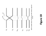
- FIG. 1A is a simplified diagram illustrating a conventional differential amplifier circuit.
- FIG. 1B is a simplified diagram illustrating electrical characteristics of a conventional differential amplifier circuit.
- FIG. 2 is a simplified diagram illustrating a liner driver apparatus according to an embodiment of the present invention.
- FIG. 3 is a simplified diagram illustrating a liner driver apparatus with a pre driver module according to an embodiment of the present invention.
- FIG. 4 is a simplified diagram illustrating a liner driver apparatus with a voltage divider module according to an embodiment of the present invention.
- FIGS. 5A and 5B are simplified diagrams illustrating swing voltages of line driver devices according to embodiments of the present invention.
- the present invention is directed to electrical circuits and techniques thereof. More specifically, an embodiment of the present invention provides a line driver with transistors directly coupled to the ground, and a bias voltage is coupled common mode resistors of the line driver. There are other embodiments as well.
- FIG. 1A is a simplified diagram illustrating a conventional differential amplifier circuit.
- Switches M 1 and M 2 form a differential amplifier pair.
- switches M 1 and M 2 are implemented using NMOS switches, and they are coupled to voltage supply V DD via their respective load resistors.
- Source terminals of the NMOS switches M 1 and M 2 are coupled to a “long tail”, which can be a tail current source 101 as shown in FIG. 1A .
- the tail current source 101 comprises a transistor switch and a tail capacitor.
- a bias current source is typically coupled to the transistor switch (M 0 ) of the tail current source 101 .
- using a current source/sink in the “tail” is common configuration in amplifier circuits.
- the long tail component is provided to improve the common mode capability of the circuit. Common mode signals are those that are applied to both inputs in the same polarity, and are generally required to be rejected. Using a simple resistive tail limits the common mode voltage that can be accommodated before severe distortion occurs.
- the tail current source 101 as shown in FIG. 1A typically consumes about 100 ⁇ 200 mV drain to the source voltage, which reduces the swing voltage of the differential amplifier. Additionally, the tail current source 101 has a capacitance (e.g., capacitor C tail ), which often leads to a voltage glitch on the drain and causes tail current variation before and after the input voltage transition, as illustrated in FIG. 1B .
- a capacitance e.g., capacitor C tail
- FIG. 1B is a simplified diagram illustrating electrical characteristics of a conventional differential amplifier circuit. As shown, during the time period between 110 and 111, input voltage V 1 transitions from high to low, and input voltage V 2 transitions from low to high. The tail voltage V tail and tail current I tail both show a “glitch” transition, which translates to current variation for I M1 and I M2 respectively at the switches M 1 and M 2 .
- the tail current source In addition to undesirable tail current variation, the tail current source also contributes to a tail node capacitance that decreases the switching speed, which can be highly undesirable in high speed communication applications.
- the tail current source can also lead to signal-dependent glitches in DFE response.
- tail current source may cause linearity problems as well.
- tail current source is often associated with jitter and common mode output noise in high current driver systems.
- embodiments of the present invention provide line driver systems implemented using differential amplifiers without the “long tail” configuration.
- line driver systems according to the present invention are configured with defined bias current source through feedback mechanism, thus removing the need for the “long tail” configuration.
- any element in a claim that does not explicitly state “means for” performing a specified function, or “step for” performing a specific function, is not to be interpreted as a “means” or “step” clause as specified in 35 U.S.C. Section 112, Paragraph 6.
- the use of “step of” or “act of” in the Claims herein is not intended to invoke the provisions of 35 U.S.C. 112, Paragraph 6.
- FIG. 2 is a simplified diagram illustrating a liner driver apparatus according to an embodiment of the present invention.
- This diagram is merely an example, which should not unduly limit the scope of the claims.
- One of ordinary skill in the art would recognize many variations, alternatives, and modifications.
- embodiments of the present invention use a predefined bias current through a feedback system, which removes the need for tail current source.
- a pair of NMOS switches provides a differential pair, which includes switch 205 and switch 206 .
- the differential pair can be implemented using a pair of PMOS transistors.
- the source terminals of switches 205 and switch 206 directly couple to a ground terminal.
- the gate of switches 205 and switch 206 are coupled to differential input signals.
- the drain terminal of switch 205 is coupled to load resistor 203 and common resistor 207 .
- the load resistor 203 is coupled to the voltage supply V DD 201 .
- the drain terminal of switch 204 is coupled to load resistor 202 and common resistor 208 .
- the load resistor 202 is coupled to the voltage supply V DD 202 . It is to be appreciated that the range of voltage swing is defined by the voltage supply V DD . In contrast, the swing voltage of a conventional differential amplifier (e.g., as illustrated in FIG.
- the differential output (which is characterized by a gain value of the differential amplifier) is provided between a switch and its load resistor (e.g., between switch 205 and load resistor 203 , or between switch 204 and load resistor 202 ).
- Common resistor 207 is coupled to load resistor 203 and switch 205 .
- Common resistor 208 is coupled to load resistor 202 and switch 204 .
- a common voltage terminal 206 is configured between common resistor 206 and common resistor 207 . As explained above, the common voltage terminal provides a common voltage V CM , which is used for a defined bias current through a feedback mechanism.
- FIG. 3 is a simplified diagram illustrating a liner driver apparatus with a pre driver module according to an embodiment of the present invention.
- a line driver apparatus includes, a pre-driver section 310 , amplifier section 320 , an operational amplifier 303 , a bias resistor 301 , and a bias current source 302 .
- a differential amplifier configuration is provided by switches 325 and 326 .
- switches 325 and 326 are implemented using NMOS transistors as shown, but it is understood that other types of devices may be used as well.
- the source terminals of switches 325 and switch 326 are directly coupled to a ground terminal as shown. As explained above, by not having a tail current source coupled to the source terminals of switches 325 and switch 326 , the swing voltage range of the amplifier section 320 is defined by the supply voltage V DD 304 . Input signals switches 325 and switch 326 are received from the pre driver section 310 .
- the drain terminal of switch 326 is coupled to load resistor 321 and common resistor 324 .
- the load resistor 321 is coupled to the voltage supply V DD 304 .
- the drain terminal of switch 325 is coupled to load resistor 322 and common resistor 323 .
- the load resistor 322 is coupled to the voltage supply V DD 304 .
- the range of voltage swing is defined by the voltage supply V DD .
- the swing voltage of a conventional differential amplifier e.g., as illustrated in FIG. 1A
- the tail current source by an amount V tail .
- the differential output (which is characterized by a gain value of the differential amplifier) is provided between a switch and its load resistor (e.g., between switch 326 and load resistor 321 , or between switch 325 and load resistor 322 ).
- Common resistor 324 is coupled to load resistor 321 and switch 326 .
- Common resistor 323 is coupled to load resistor 322 and switch 325 .
- a common voltage terminal 329 is configured between common resistor 324 and common resistor 323 .
- the resistances of resistor 321 and resistor 322 are matched to be close to each other (e.g., less than 1% difference in resistance value); resistances of resistor 324 and resistor 323 are similarly matched.
- the resistance value of the load resistors are much less than resistance value of the common resistors.
- the common resistors 323 and 324 may have a resistance value of about 10K ohms, while the load resistors 321 and 322 have a resistance value of about 50 ohms.
- the resistance value ratio between load resistors and common resistors helps reduce amount of common mode signal at terminal 329 .
- the common voltage terminal 329 is provided as an input to the amplifier 303 as shown.
- the pre driver section 310 includes switch 311 (switch M 5 ) that is coupled to voltage supply and the output of amplifier 303 .
- amplifier 303 comprises an operation amplifier device.
- amplifier 303 is configured as part of a feedback mechanism, who inputs include common voltage terminal 329 and a reference bias voltage defined by the bias resistor 301 (R bias ) and the bias current source 302 (I bias ).
- the common voltage terminal 329 coming from the amplifier section 320 , provides a feedback for the line driver system. By comparing inputs from common voltage terminal 329 and the reference bias voltage, the amplifier 303 provides an output that adjusts the gate voltage of switch 311 .
- switch 311 comprises a PMOS transistor.
- the common mode voltage between switch 312 and switch 313 is in turn controlled by the output of switch 311 .
- Switch 312 and switch 313 are implemented using PMOS transistors.
- the gate of switch 312 is coupled to input I np .
- the gate of switch 313 is coupled to input I nn .
- Switch 312 and switch 313 are respectively coupled to resistor 314 and resistor 315 .
- resistor 314 and resistor 315 function as load resistors respectively for switch 312 and switch 315 .
- the output of switch 312 is coupled to the gate of switch 326 .
- the output of switch 313 is coupled to the gate of switch 325 .
- the amplifier section 320 are implemented with two NMOS transistors for switch 325 and switch 326 .
- the pre-driver section 310 include two PMOS transistors for switch 312 and switch 313 .
- the amplifier section 320 is implemented with two PMOS transistors, and the pre-driver section 310 is implemented using NMOS transistors.
- the output of the switches are coupled to load resistors.
- the output of switch 312 is coupled to resistor 314 .
- Output of switch 313 is coupled to resistor 315 .
- resistor 314 and resistor 315 function as output devices for the pre driver section 310 .
- other types of output devices may be used.
- NMOS transistors can be used as output devices for pre driver section 310 .
- the output devices for pre driver section 310 may be based on the speed requirement of communication systems.
- V DD and V SS noises sometimes appear as common mode noises, which is similar to the noise profiles of conventional differential amplifier implementations.
- actual device performance is affected by pressure, voltage, and temperature (PVT). More specifically, swing voltage of the driver system can be affected by the PVT system.
- PVT pressure, voltage, and temperature
- the configuration of the line driver system illustrated in FIG. 3 is specifically implemented to match the system load and output devices.
- FIG. 4 is a simplified diagram illustrating a liner driver apparatus with a voltage divider module according to an embodiment of the present invention.
- This diagram is merely an example, which should not unduly limit the scope of the claims.
- One of ordinary skill in the art would recognize many variations, alternatives, and modifications.
- a pair of NMOS switches provides a differential pair, which includes switch 410 and switch 409 .
- other types of switches e.g., PMOS transistors
- the source terminals of switches 410 and switch 409 directly couple to a ground terminal.
- the gate of switches 410 and switch 409 are coupled to differential input signals.
- the drain terminal of switch 410 is coupled to load resistor 405 and common resistor 408 .
- the load resistor 405 is coupled to the voltage supply V DD 404 .
- the drain terminal of switch 409 is coupled to load resistor 406 and common resistor 407 .
- the load resistor 406 is coupled to the voltage supply V DD 404 . It is to be appreciated that the range of voltage swing is defined by the voltage supply V DD . In contrast, the swing voltage of a conventional differential amplifier (e.g., as illustrated in FIG. 1A ) is reduced by the tail current source by an amount V tail .
- the differential output (which is characterized by a gain value of the differential amplifier) is provided between a switch and its load resistor (e.g., between switch 410 and load resistor 405 , or between switch 409 and load resistor 406 ).
- Common resistor 408 is coupled to load resistor 405 and switch 410 .
- Common resistor 407 is coupled to load resistor 406 and switch 409 .
- a common voltage terminal 420 is configured between common resistor 408 and common resistor 407 .
- the common voltage terminal provides a common voltage V CM , which is used for a defined bias current through a feedback mechanism.
- the common voltage terminal 420 is provided between resistor 402 and resistor 403 .
- resistor 402 and resistor 403 are configured in series and form a voltage divider between bias voltage 401 and the ground terminal.
- the ratio of resistance values between resistor 402 and resistor 403 is predefined based on the actual implementations.
- FIGS. 5A and 5B are simplified diagrams illustrating swing voltage of line driver devices according to embodiments of the present invention. This diagram is merely an example, which should not unduly limit the scope of the claims. One of ordinary skill in the art would recognize many variations, alternatives, and modifications.
- a conventional different amplifier device includes a tail current source (M 0 ) that is characterized by a voltage of 100 mV, which effectively reduces the peak-to-peak (P2P) swing voltage of the different amplifier by a 100 mV.
- P2P peak-to-peak
- Vth 500 mV
- a differential amplifier device eliminates the need for a tail current source.
- the P2P differential swing voltage of a differential amplifier according to embodiments of the present invention is increased.
- V th 400 mV
- differential amplifiers according to embodiments of the present invention afford a bigger P2P swing voltage when compared to conventional devices.
- line driver devices and differential amplifier devices according to embodiments of the present invention provide many other advantages over conventional devices.
Landscapes
- Engineering & Computer Science (AREA)
- Power Engineering (AREA)
- Amplifiers (AREA)
Abstract
Description
Assume Vth=500 mV
Minimum bias voltage V b required for cascade=V th3+ Vds 1+ Vds 3+ vds 0=500 m+100 m+100 m+100 m=800 m
Min voltage of M3 drain=Vb−Vth3=300 mV
P2P differential swing=2*(Vdd−Vb+Vth3)=3v
Assume threshold voltage V th=400 mV
Minimum bias voltage V b required for cascode=V th3+ Vds 1+ Vds 3=500 m+100 m+100 m=700 m
Min voltage of M3 drain=Vb−Vth3=200 mV
P2P differential swing=2*(Vdd−Vb+Vth3)=3.2v
Claims (14)
Priority Applications (2)
| Application Number | Priority Date | Filing Date | Title |
|---|---|---|---|
| US15/201,287 US9847762B1 (en) | 2016-07-01 | 2016-07-01 | Low voltage high speed CMOS line driver without tail current source |
| US15/811,036 US10122335B2 (en) | 2016-07-01 | 2017-11-13 | Low voltage high speed CMOS line driver without tail current source |
Applications Claiming Priority (1)
| Application Number | Priority Date | Filing Date | Title |
|---|---|---|---|
| US15/201,287 US9847762B1 (en) | 2016-07-01 | 2016-07-01 | Low voltage high speed CMOS line driver without tail current source |
Related Child Applications (1)
| Application Number | Title | Priority Date | Filing Date |
|---|---|---|---|
| US15/811,036 Continuation US10122335B2 (en) | 2016-07-01 | 2017-11-13 | Low voltage high speed CMOS line driver without tail current source |
Publications (1)
| Publication Number | Publication Date |
|---|---|
| US9847762B1 true US9847762B1 (en) | 2017-12-19 |
Family
ID=60629269
Family Applications (2)
| Application Number | Title | Priority Date | Filing Date |
|---|---|---|---|
| US15/201,287 Active US9847762B1 (en) | 2016-07-01 | 2016-07-01 | Low voltage high speed CMOS line driver without tail current source |
| US15/811,036 Active US10122335B2 (en) | 2016-07-01 | 2017-11-13 | Low voltage high speed CMOS line driver without tail current source |
Family Applications After (1)
| Application Number | Title | Priority Date | Filing Date |
|---|---|---|---|
| US15/811,036 Active US10122335B2 (en) | 2016-07-01 | 2017-11-13 | Low voltage high speed CMOS line driver without tail current source |
Country Status (1)
| Country | Link |
|---|---|
| US (2) | US9847762B1 (en) |
Cited By (2)
| Publication number | Priority date | Publication date | Assignee | Title |
|---|---|---|---|---|
| US10491166B2 (en) | 2018-03-01 | 2019-11-26 | Semiconductor Components Industries, Llc | Low noise differential amplifier |
| CN110995267A (en) * | 2019-11-08 | 2020-04-10 | 芯创智(北京)微电子有限公司 | Dynamic comparator, electronic equipment and implementation method thereof |
Citations (8)
| Publication number | Priority date | Publication date | Assignee | Title |
|---|---|---|---|---|
| US5008632A (en) * | 1989-10-31 | 1991-04-16 | International Business Machines Corporation | Temperature compensated feedback circuit for setting and stabilizing amplifier DC bias points |
| US6429700B1 (en) * | 2001-04-17 | 2002-08-06 | International Business Machines Corporation | Driver circuit with output common mode voltage control |
| US6664814B1 (en) * | 2002-07-18 | 2003-12-16 | Cadence Design Systems, Inc. | Output driver for an integrated circuit |
| US7271651B2 (en) * | 2005-06-17 | 2007-09-18 | Agere Systems Inc. | High performance differential amplifiers with thick oxide devices for high impedance nodes |
| US7330075B2 (en) * | 2004-01-30 | 2008-02-12 | Realtek Semiconductor Corp. | Output impedance control circuit and control method thereof |
| US20090267693A1 (en) * | 2008-04-25 | 2009-10-29 | Chandra Gaurav | Resistor self-trim circuit for increased performance |
| US7924094B2 (en) * | 2008-06-02 | 2011-04-12 | Renesas Electronics Corporation | Amplifier and offset regulating circuit |
| US8310308B1 (en) * | 2011-05-31 | 2012-11-13 | Texas Instruments Incorporated | Wide bandwidth class C amplifier with common-mode feedback |
Family Cites Families (4)
| Publication number | Priority date | Publication date | Assignee | Title |
|---|---|---|---|---|
| US6356141B1 (en) * | 1999-04-06 | 2002-03-12 | Matsushita Electric Industrial Co., Ltd. | Constant-current output circuit |
| US6731135B2 (en) * | 2001-06-14 | 2004-05-04 | Artisan Components, Inc. | Low voltage differential signaling circuit with mid-point bias |
| US6661288B2 (en) * | 2002-02-09 | 2003-12-09 | Texas Instruments Incorporated | Apparatus for effecting high speed switching of a communication signal |
| US9209789B1 (en) * | 2014-08-13 | 2015-12-08 | Qualcomm Incorporated | Apparatus to convert electrical signals from small-signal format to rail-to-rail format |
-
2016
- 2016-07-01 US US15/201,287 patent/US9847762B1/en active Active
-
2017
- 2017-11-13 US US15/811,036 patent/US10122335B2/en active Active
Patent Citations (8)
| Publication number | Priority date | Publication date | Assignee | Title |
|---|---|---|---|---|
| US5008632A (en) * | 1989-10-31 | 1991-04-16 | International Business Machines Corporation | Temperature compensated feedback circuit for setting and stabilizing amplifier DC bias points |
| US6429700B1 (en) * | 2001-04-17 | 2002-08-06 | International Business Machines Corporation | Driver circuit with output common mode voltage control |
| US6664814B1 (en) * | 2002-07-18 | 2003-12-16 | Cadence Design Systems, Inc. | Output driver for an integrated circuit |
| US7330075B2 (en) * | 2004-01-30 | 2008-02-12 | Realtek Semiconductor Corp. | Output impedance control circuit and control method thereof |
| US7271651B2 (en) * | 2005-06-17 | 2007-09-18 | Agere Systems Inc. | High performance differential amplifiers with thick oxide devices for high impedance nodes |
| US20090267693A1 (en) * | 2008-04-25 | 2009-10-29 | Chandra Gaurav | Resistor self-trim circuit for increased performance |
| US7924094B2 (en) * | 2008-06-02 | 2011-04-12 | Renesas Electronics Corporation | Amplifier and offset regulating circuit |
| US8310308B1 (en) * | 2011-05-31 | 2012-11-13 | Texas Instruments Incorporated | Wide bandwidth class C amplifier with common-mode feedback |
Cited By (3)
| Publication number | Priority date | Publication date | Assignee | Title |
|---|---|---|---|---|
| US10491166B2 (en) | 2018-03-01 | 2019-11-26 | Semiconductor Components Industries, Llc | Low noise differential amplifier |
| US10756680B2 (en) | 2018-03-01 | 2020-08-25 | Semiconductor Components Industries, Llc | Low noise differential amplifier |
| CN110995267A (en) * | 2019-11-08 | 2020-04-10 | 芯创智(北京)微电子有限公司 | Dynamic comparator, electronic equipment and implementation method thereof |
Also Published As
| Publication number | Publication date |
|---|---|
| US10122335B2 (en) | 2018-11-06 |
| US20180069514A1 (en) | 2018-03-08 |
Similar Documents
| Publication | Publication Date | Title |
|---|---|---|
| EP3437187B1 (en) | System and method for controlling common mode voltage via replica circuit and feedback control | |
| US9746864B1 (en) | Fast transient low drop-out voltage regulator for a voltage-mode driver | |
| US6252435B1 (en) | Complementary differential amplifier with resistive loads for wide common-mode input range | |
| US8102211B2 (en) | Rail-to-rail input stage circuit with dynamic bias control | |
| US9013222B2 (en) | Equalizer circuit and receiver circuit including the same | |
| EP1461923A1 (en) | Low supply voltage differential signal driver | |
| US7782142B2 (en) | High speed differential to single ended converting circuit | |
| US8841970B2 (en) | Low GM transconductor | |
| US9407221B2 (en) | Differential amplifier circuit | |
| US7969218B2 (en) | Receiver for reducing intersymbol interference of a channel and compensating for signal gain loss, and method thereof | |
| CN113259279B (en) | Equalizer | |
| US7764086B2 (en) | Buffer circuit | |
| US10122335B2 (en) | Low voltage high speed CMOS line driver without tail current source | |
| US8149056B2 (en) | Amplifying circuit | |
| US11362629B2 (en) | Transimpedance amplifier circuit | |
| JP4957405B2 (en) | Signal waveform equalization circuit and reception circuit | |
| US8963637B2 (en) | Semiconductor device and communication device | |
| US8008972B2 (en) | Differential signal generator circuit | |
| US8803611B2 (en) | Current mode logic circuit and method | |
| US10205423B1 (en) | Rail-to-rail source follower | |
| US6686794B1 (en) | Differential charge pump | |
| US9998120B1 (en) | Circuit for and method of shifting a high range input common mode voltage | |
| US7312658B2 (en) | Differential amplifier with two outputs and a single input of improved linearity | |
| US9590607B2 (en) | Input buffer circuit | |
| US8803601B2 (en) | Amplifying circuit |
Legal Events
| Date | Code | Title | Description |
|---|---|---|---|
| AS | Assignment |
Owner name: INPHI CORPORATION, CALIFORNIA Free format text: ASSIGNMENT OF ASSIGNORS INTEREST;ASSIGNORS:NAGULAPALLI, RAJASEKHAR;FOREY, SIMON;MISHRA, PARMANAND;SIGNING DATES FROM 20160629 TO 20160630;REEL/FRAME:039275/0944 |
|
| FEPP | Fee payment procedure |
Free format text: ENTITY STATUS SET TO UNDISCOUNTED (ORIGINAL EVENT CODE: BIG.) |
|
| STCF | Information on status: patent grant |
Free format text: PATENTED CASE |
|
| MAFP | Maintenance fee payment |
Free format text: PAYMENT OF MAINTENANCE FEE, 4TH YEAR, LARGE ENTITY (ORIGINAL EVENT CODE: M1551); ENTITY STATUS OF PATENT OWNER: LARGE ENTITY Year of fee payment: 4 |
|
| AS | Assignment |
Owner name: MARVELL TECHNOLOGY CAYMAN I, CAYMAN ISLANDS Free format text: ASSIGNMENT OF ASSIGNORS INTEREST;ASSIGNOR:INPHI CORPORATION;REEL/FRAME:056649/0823 Effective date: 20210617 |
|
| AS | Assignment |
Owner name: CAVIUM INTERNATIONAL, CAYMAN ISLANDS Free format text: ASSIGNMENT OF ASSIGNORS INTEREST;ASSIGNOR:MARVELL TECHNOLOGY CAYMAN I;REEL/FRAME:057279/0519 Effective date: 20210620 |
|
| AS | Assignment |
Owner name: MARVELL ASIA PTE LTD., SINGAPORE Free format text: ASSIGNMENT OF ASSIGNORS INTEREST;ASSIGNOR:CAVIUM INTERNATIONAL;REEL/FRAME:057336/0873 Effective date: 20210620 |