US9842989B2 - Magnetic memory with high thermal budget - Google Patents
Magnetic memory with high thermal budget Download PDFInfo
- Publication number
- US9842989B2 US9842989B2 US15/057,107 US201615057107A US9842989B2 US 9842989 B2 US9842989 B2 US 9842989B2 US 201615057107 A US201615057107 A US 201615057107A US 9842989 B2 US9842989 B2 US 9842989B2
- Authority
- US
- United States
- Prior art keywords
- layer
- seed
- layers
- forming
- orientation
- Prior art date
- Legal status (The legal status is an assumption and is not a legal conclusion. Google has not performed a legal analysis and makes no representation as to the accuracy of the status listed.)
- Expired - Fee Related
Links
Images


Classifications
-
- H—ELECTRICITY
- H10—SEMICONDUCTOR DEVICES; ELECTRIC SOLID-STATE DEVICES NOT OTHERWISE PROVIDED FOR
- H10B—ELECTRONIC MEMORY DEVICES
- H10B61/00—Magnetic memory devices, e.g. magnetoresistive RAM [MRAM] devices
- H10B61/20—Magnetic memory devices, e.g. magnetoresistive RAM [MRAM] devices comprising components having three or more electrodes, e.g. transistors
- H10B61/22—Magnetic memory devices, e.g. magnetoresistive RAM [MRAM] devices comprising components having three or more electrodes, e.g. transistors of the field-effect transistor [FET] type
-
- H01L43/12—
-
- H01L27/228—
-
- H01L43/02—
-
- H01L43/08—
-
- H01L43/10—
-
- H—ELECTRICITY
- H10—SEMICONDUCTOR DEVICES; ELECTRIC SOLID-STATE DEVICES NOT OTHERWISE PROVIDED FOR
- H10N—ELECTRIC SOLID-STATE DEVICES NOT OTHERWISE PROVIDED FOR
- H10N50/00—Galvanomagnetic devices
- H10N50/01—Manufacture or treatment
-
- H—ELECTRICITY
- H10—SEMICONDUCTOR DEVICES; ELECTRIC SOLID-STATE DEVICES NOT OTHERWISE PROVIDED FOR
- H10N—ELECTRIC SOLID-STATE DEVICES NOT OTHERWISE PROVIDED FOR
- H10N50/00—Galvanomagnetic devices
- H10N50/10—Magnetoresistive devices
-
- H—ELECTRICITY
- H10—SEMICONDUCTOR DEVICES; ELECTRIC SOLID-STATE DEVICES NOT OTHERWISE PROVIDED FOR
- H10N—ELECTRIC SOLID-STATE DEVICES NOT OTHERWISE PROVIDED FOR
- H10N50/00—Galvanomagnetic devices
- H10N50/80—Constructional details
-
- H—ELECTRICITY
- H10—SEMICONDUCTOR DEVICES; ELECTRIC SOLID-STATE DEVICES NOT OTHERWISE PROVIDED FOR
- H10N—ELECTRIC SOLID-STATE DEVICES NOT OTHERWISE PROVIDED FOR
- H10N50/00—Galvanomagnetic devices
- H10N50/80—Constructional details
- H10N50/85—Materials of the active region
Definitions
- a magnetic memory cell or device stores information by changing electrical resistance of a magnetic tunnel junction (MTJ) element.
- the MTJ element typically includes a thin insulating tunnel barrier layer sandwiched between a magnetically fixed layer and a magnetically free layer, forming a magnetic tunnel junction. Magnetic orientations of the fixed and free layers may be in a vertical direction, forming a perpendicular MTJ (or pMTJ) element.
- the pMTJ element could be either in a bottom pinned pMTJ element or a top pinned pMTJ element.
- the bottom pinned pMTJ element is formed by having the magnetically fixed layer disposed below the magnetically free layer while the top pinned pMTJ element is formed by having the fixed layer disposed above the free layer.
- Embodiments of the present disclosure generally relate to semiconductor devices and methods for forming a semiconductor device.
- a method of forming a memory cell includes forming a select unit on a substrate.
- the select unit includes a transistor having a first source/drain (S/D) region, a second S/D region, and a gate between the first and second S/D regions.
- a dielectric layer is formed on the substrate covering the select unit.
- the dielectric layer includes storage pad coupled to the first S/D region.
- a storage unit is formed on the storage pad.
- Forming the storage unit includes forming a bottom electrode and forming a fixed layer over the bottom electrode.
- the fixed layer includes a hard layer disposed over a base layer.
- the base layer promotes face-centered cubic (FCC) structure along (111) orientation to increase perpendicular anisotropy.
- the base layer includes a wetting layer and a seed layer.
- the seed layer includes a first seed layer, a roughness smoother to improve surface smoothness of the first seed layer and a second seed layer formed over the roughness smoother.
- the roughness smoother improves surface smoothness of the second seed layer.
- a hard layer is formed over the seed layer. Improved surface smoothness of the seed layer improves surface smoothness of the hard layer to improve thermal endurance.
- Forming the storage unit includes forming at least one tunneling barrier layer over the hard layer, forming a storage layer over the tunneling barrier layer, and forming a top electrode over the storage layer.
- the method also includes forming a bitline coupled to the top electrode layer.
- FIG. 1 shows simplified diagrams of parallel state and anti-parallel state of a bottom pinned perpendicular MTJ element of a magnetic memory cell.
- FIG. 2 shows a schematic diagram of an embodiment of a magnetic memory cell.
- FIG. 3 shows an array of magnetic memory cells.
- FIG. 4 shows a cross-sectional view of an embodiment of a memory cell.
- FIGS. 5 a -5 b show cross-sectional views of embodiments of a storage unit of magnetic memory cell.
- FIGS. 6 a -6 b show cross-sectional views of embodiments of a storage unit of magnetic memory cell.
- FIG. 7 a -7 l show cross-sectional views of an embodiment of a process for forming a memory cell
- Embodiments of the present disclosure generally relate to memory cells or devices.
- the memory cells are magnetoresistive memory cells.
- the memory devices may be spin transfer torque magnetoresistive random access memory (STT-MRAM) devices.
- a magnetoresistive memory cell includes a magnetic tunneling junction (MTJ) storage unit.
- the MTJ storage unit of the present disclosure includes a base layer having a seed layer with roughness smoother or crystallinity enhancing layer and a wetting layer that provides an improved PMA of the fixed layer of the pMTJ stack and further enhances the thermal endurance and thermal budget of the pMTJ stack.
- Other suitable types of memory cells may also be useful.
- Such memory devices may be incorporated into standalone memory devices including, but not limited to, USB or other types of portable storage units, or ICs, such as microcontrollers or system on chips (SoCs).
- ICs such as microcontrollers or system on chips (SoCs).
- SoCs system on chips
- the devices or ICs may be incorporated into or used with, for example, consumer electronic products, or relate to other types of devices.
- FIG. 1 shows a simplified cross-sectional view of an embodiment of a bottom pinned perpendicular MTJ (pMTJ) unit 110 of a magnetic or memory cell.
- the MTJ unit includes a pMTJ element or stack 120 disposed between a bottom electrode 131 and a top electrode 132 .
- the bottom electrode is proximate to the substrate on which the memory cell is formed while the top electrode is distal from the substrate.
- the MTJ element includes a magnetically fixed (pinned) layer 126 , a tunneling barrier layer 127 and a magnetically free layer 128 .
- the magnetically fixed layer is disposed below the magnetic free layer, forming a bottom pinned pMTJ stack.
- the magnetic orientation of the fixed layer is fixed in a first perpendicular direction.
- the term perpendicular direction refers to the direction which is perpendicular to the surface of a substrate or perpendicular to the plane of the layers of the MTJ element. As shown, the first perpendicular direction is in an upward direction away from the substrate. Providing the first perpendicular direction which is in a downward direction towards the substrate may also be useful.
- the magnetic orientation of the free layer it may be programmed to be in a first or same direction as the fixed layer or in a second or opposite direction as the fixed layer.
- the magnetic direction of the free layer is programmed to be in the second or anti-parallel direction to the fixed layer.
- the corresponding MTJ electrical resistance between the free layer 128 and the fixed layer 126 is denoted as R AP .
- Structure 112 illustrates that the magnetization of the free layer is programmed to be in the first or parallel direction to the fixed layer.
- the corresponding MTJ electrical resistance between the free layer 128 and the fixed layer 126 is denoted as R P .
- the resistance R AP is higher than the resistance R P .
- FIG. 2 shows a schematic diagram of an embodiment of a memory cell 200 .
- the memory cell is a non-volatile memory cell.
- the memory cell may be a magnetoresistive memory cell.
- the memory cell is a Spin Transfer Torque-Magnetoresistive Random Access Memory (STT-MRAM) cell.
- STT-MRAM Spin Transfer Torque-Magnetoresistive Random Access Memory
- the memory cell includes a magnetic storage unit 210 and a cell selector unit 240 .
- the storage unit is coupled to the cell selector unit.
- the storage unit and cell selector unit are coupled at a first cell node 239 of the memory cell.
- the storage unit 210 in one embodiment, is a magnetic storage unit and includes a pMTJ element 220 .
- the pMTJ element may be similar to that described in FIG. 1 .
- Other suitable types of MTJ elements may also be useful.
- the pMTJ element includes first and second electrodes 231 and 232 .
- the first electrode for example, may be a bottom electrode while the second electrode may be a top electrode. Other configurations of electrodes may also be useful.
- the top electrode of the storage unit is electrically connected to a bit line (BL).
- the bottom electrode of the storage element is connected to the first cell node 239 .
- the cell selector unit includes a selector for selecting the memory cell.
- the selector for example, may be a select transistor.
- the select transistor is a metal oxide semiconductor (MOS) transistor.
- the selector is a n-type MOS transistor.
- the select transistor includes first and second source/drain (S/D) terminals 245 and 246 and a gate or control terminal 244 .
- the first S/D terminal may be referred to as a drain and the second S/D terminal may be referred to as the source.
- the S/D terminals for example, are heavily doped regions with first polarity type dopants, defining the first type transistor.
- the S/D terminals are n-type heavily doped regions.
- Other types of transistors or selectors may also be useful.
- the first terminal of the cell selector and first electrode of the storage unit are commonly coupled at the first cell node.
- the first S/D terminal of the cell selector is coupled to the bottom electrode of the storage unit.
- the drain terminal is coupled to the storage unit.
- the second or source terminal of the cell selector is coupled to a source line (SL).
- SL source line
- the gate terminal it is coupled to a wordline WL.
- FIG. 3 shows a schematic diagram of an embodiment of a memory array 300 .
- the array includes a plurality of memory cells 200 interconnected.
- the memory cells may be similar to those described in FIG. 2 .
- the memory cells are MRAM cells, such as STT-MRAM cells. Common elements may not be described or described in detail. Other suitable types of memory cells may also be useful.
- the array includes four memory cells arranged in a 2 ⁇ 2 array.
- the array is arranged to form two rows and two columns of memory cells.
- Memory cells of a row are interconnected by a wordline (WL 1 or WL 2 ) while memory cells of a column are interconnected by a bitline (BL 1 or BL 2 ).
- a second S/D or source terminal is coupled to a source line (SL 1 or SL 2 ).
- the SLs are in the row or wordline direction.
- Other suitable cell configurations may also be useful.
- the array is illustrated as a 2 ⁇ 2 array, it is understood that arrays of other sizes may also be useful.
- FIG. 4 shows a cross-sectional view of an exemplary embodiment of a memory cell 400 of a device.
- the cross-sectional view for example is along a second or bitline direction of the device.
- the device includes a memory cell 400 .
- the memory cell for example, may be a NVM memory cell.
- the memory cell in one embodiment, is a magnetoresistive NVM cell, such as a STT-MRAM cell.
- the memory cell for example, is similar to that described in FIG. 2 . Common elements may not be described or described in detail.
- the memory cell is disposed on a substrate 405 .
- the memory cell is disposed in a cell region of the substrate.
- the cell region may be part of an array region.
- the array region may include a plurality of cell regions.
- the substrate may include other types of device regions (not shown), such as high voltage (HV) as well as logic regions, including low voltage (LV) and intermediate voltage (IV) device regions. Other types of regions may also be provided.
- HV high voltage
- LV low voltage
- IV intermediate voltage
- the substrate for example, is a semiconductor substrate, such as a silicon substrate.
- the substrate may be a lightly doped p-type substrate. Providing an intrinsic or other types of doped substrates, such as silicon-germanium (SiGe), germanium (Ge), gallium-arsenic (GaAs) or any other suitable semiconductor materials, may also be useful.
- the substrate may be a crystalline-on-insulator (COI) substrate.
- a COI substrate includes a surface crystalline layer separated from a crystalline bulk by an insulator layer.
- the insulator layer for example, may be formed of a dielectric insulating material.
- the insulator layer for example, is formed from silicon oxide, which provides a buried oxide (BOX) layer. Other types of dielectric insulating materials may also be useful.
- the COI substrate for example, is a silicon-on-insulator (SOI) substrate.
- SOI silicon-on-insulator
- the surface and bulk crystalline layers are single crystalline silicon. Other types of COI substrates may also be useful. It is understood that the surface and bulk layers need not be formed of the same material.
- Front-end-of-line (FEOL) processing is performed on the substrate.
- the FEOL process for example, forms n-type and p-type devices or transistors on the substrate.
- the p-type and n-type device form a complementary MOS (CMOS) device.
- CMOS complementary MOS
- the FEOL processing for example, includes forming isolation regions, various device and isolation wells, transistor gates and transistor source/drain (S/D) regions and contact or diffusion regions serving as substrate or well taps. Forming other components with the FEOL process may also be useful.
- Isolation regions 480 serve to isolate different device regions.
- the isolation regions may be shallow trench isolation (STI) region.
- STI shallow trench isolation
- CMP chemical mechanical polishing
- isolation regions are provided to isolate device regions from other regions.
- Device wells serve as bodies of p-type and n-type transistors.
- Device wells are doped wells.
- Second type doped device wells serve as bodies of first type transistors.
- p-type device wells serve as bodies of n-type transistors
- n-type device wells serve as bodies of p-type transistors.
- Isolation wells may be used to isolate device wells from the substrate.
- the isolation wells are deeper than the device wells.
- isolation wells encompass the device wells.
- the isolation wells are first type doped wells.
- n-type isolation wells are used to isolate p-type device wells. Separate implants may be employed to form different doped device wells and isolation wells using, for example, implant masks, such as photoresist masks.
- the wells for example, are formed after forming isolation regions.
- Gates of transistors are formed on the substrate.
- layers of the gate such as gate dielectric and gate electrode are formed on the substrate and patterned to form the gates.
- the gate dielectric may be a silicon oxide layer while the gate electrode layer may be polysilicon.
- the gate electrode may be doped, for example, to reduce sheet resistance. Other types of gate dielectric and gate electrode layers may also be useful.
- the gate dielectric layer may be formed by thermal oxidation and the gate electrode layer may be formed by chemical vapor deposition (CVD). Separate processes may be performed for forming gate dielectrics of the different voltage transistors. This is due to, for example, different gate dielectric thicknesses associated with the different voltage transistors. For example, HV transistor will have a thicker gate dielectric than a LV transistor.
- the gate layers are patterned by, for example, mask and etch techniques.
- a patterned photoresist mask may be provided over the gate layers.
- a photoresist layer is formed over the gate layers and lithographically exposed by using a reticle.
- the mask layer is developed, forming a patterned mask with the desired pattern of the reticle.
- an anti-reflective coating (ARC) layer may be provided between the gate layer and resist mask layer.
- An anisotropic etch, such as a reactive ion etch (RIE) is used to pattern the gate layers to form the gates using the patterned mask layer.
- RIE reactive ion etch
- Doped contact regions 445 and 446 are formed in exposed active regions of the substrate after forming the gates.
- the contact regions are heavily doped regions.
- the contact regions may be heavily doped n-type or p-type regions.
- S/D regions are heavily doped n-type regions and for p-type transistors, S/D regions are heavily doped p-type regions.
- well taps they are the same dopant type as the well.
- a S/D region may include lightly doped diffusion (LDD) and halo regions.
- LDD region is a lightly doped region with first polarity type dopants while the halo region is a lightly doped region with second polarity type dopants.
- the halo region includes p-type dopants for a n-type transistor while the LDD region includes n-type dopants for n-type transistors.
- the halo and LDD regions extend under the gate.
- a halo region extends farther below the gate than a LDD region.
- Other configurations of LDD, halo and S/D regions may also be useful.
- Dielectric spacers may be provided on the gate sidewalls of the transistors.
- the spacers may be used to facilitate forming transistor halo, LDD and transistor S/D regions.
- spacers are formed after halo and LDD regions are formed.
- Spacers may be formed by, for example, forming a spacer layer on the substrate and anisotropically etching it to remove horizontal portions, leaving the spacers on sidewalls of the gates. After forming the spacers, an implant is performed to form the S/D regions. Separate implants may be employed to form different doped regions using, for example, implant masks, such as photoresist mask. Well taps of the same dopant type as S/D regions are formed at the same time.
- the FEOL processing forms a cell region isolated by an isolation region 480 , such as a STI region.
- the cell region is for a memory cell. Isolation regions may be provided to isolate columns of memory cells. Other configurations of isolation regions may also be useful.
- the cell region may include a cell device well (not shown).
- the cell device well for example, serves as a body well for a transistor of the memory cell.
- the device well may be doped with second polarity type dopants for first polarity type transistors.
- the device well may be lightly or intermediately doped with second polarity type dopants.
- a cell device isolation well (not shown) may be provided, encompassing the cell device well.
- the isolation well may have a dopant type which has the opposite polarity to that of the cell device well.
- the isolation well may include first polarity type dopants.
- the isolation well serves to isolate the cell device well from the substrate.
- Well biases may be provided to bias the wells.
- the cell device well may be a common well for the cell regions in the array region.
- the cell device well may be an array well.
- the cell device isolation well may serve as the array isolation well. Other configurations of device and isolation wells may also be useful. Other device regions of the device may also include device and/or device isolation wells.
- the memory cell includes a cell selector unit 440 and a storage unit 410 .
- the FEOL forms the cell selector in the cell region.
- the cell selector unit includes a selector for selecting the memory cell.
- the selector for example, may be a select transistor.
- the select transistor is a metal oxide semiconductor (MOS) transistor.
- MOS metal oxide semiconductor
- the transistor as shown, includes first and second source/drain (S/D) regions 445 and 446 formed in the substrate and a gate 444 disposed on the substrate between the S/D regions.
- the first S/D region may be referred to as a drain region and the second S/D region may be referred to as a source region.
- the S/D regions are heavily doped regions with first polarity type dopants, defining the first type transistor.
- first polarity type dopants defining the first type transistor.
- the S/D regions are n-type heavily doped regions.
- Other types of transistors or selectors may also be useful.
- the gate it includes a gate electrode over a gate dielectric.
- the gate electrode may be polysilicon while the gate dielectric may be silicon oxide. Other types of gate electrode and gate dielectric materials may also be useful.
- a gate for example, may be a gate conductor along a first or wordline direction. The gate conductor forms a common gate for a row of memory cells.
- a S/D region may include LDD and halo regions (not shown).
- Dielectric spacers may be provided on the gate sidewalls of the transistors to facilitate forming transistor halo, LDD and transistor S/D regions. It is understood that not all transistors include LDD and/or halo regions.
- the BEOL process includes forming interconnects in interlevel dielectric (ILD) layers 490 .
- the interconnects connect the various components of the IC to perform the desired functions.
- An ILD layer includes a metal level 494 and a contact level 492 .
- the metal level includes conductors or metal lines 495 while the contact level includes contacts 493 .
- the conductors and contacts may be formed of a metal, such as copper, copper alloy, aluminum, tungsten or a combination thereof. Other suitable types of metal, alloys or conductive materials may also be useful. In some cases, the conductors and contacts may be formed of the same material.
- the conductors and contacts may be formed by dual damascene processes. This results in the conductors and contacts having the same material.
- the conductors and contacts may have different materials.
- the materials of the conductors and contacts may be different.
- Other techniques, such as reactive ion etch (RIE) may also be employed to form metal lines.
- a metal level of an ILD level may be referred to as M i , where i is from 1 to x and is the i th ILD level of x ILD levels.
- a contact level of an ILD level may be referred to as V i-1 , where i is the i th ILD level of x ILD levels.
- the BEOL process commences by forming a dielectric layer over the transistors and other components formed in the FEOL process.
- the dielectric layer may be silicon oxide.
- the dielectric layer may be silicon oxide formed by chemical vapor deposition (CVD).
- the dielectric layer serves as a premetal dielectric layer or first contact layer of the BEOL process.
- the dielectric layer may be referred to as CA level of the BEOL process.
- Contacts are formed in the CA level dielectric layer.
- the contacts may be formed by a single damascene process.
- Via openings are formed in the dielectric layer using mask and etch techniques. For example, a patterned resist mask with openings corresponding to the vias is formed over the dielectric layer.
- An anisotropic etch such as RIE, is performed to form the vias, exposing contact regions below, such as S/D regions and gates.
- a conductive layer such as tungsten is deposited on the substrate, filling the openings.
- the conductive layer may be formed by sputtering. Other techniques may also be useful.
- a planarization process such as CMP, is performed to remove excess conductive material, leaving contact plugs in the CA level.
- the BEOL process continues to form dielectric layer over the substrate, covering the CA level dielectric layer.
- the dielectric layer for example, serves as a first metal level M 1 of the first ILD layer.
- the upper dielectric layer for example, is a silicon oxide layer. Other types of dielectric layers may also be useful.
- the dielectric layer may be formed by CVD. Other techniques for forming the dielectric layer may also be useful.
- Conductive lines are formed in the M 1 level dielectric layer.
- the conductive lines may be formed by a damascene technique.
- the dielectric layer may be etched to form trenches or openings using, for example, mask and etch techniques.
- a conductive layer is formed on the substrate, filling the openings.
- a copper or copper alloy layer may be formed to fill the openings.
- the conductive material may be formed by, for example, plating, such as electro or electroless plating. Other types of conductive layers or forming techniques may also be useful. Excess conductive materials are removed by, for example, CMP, leaving planar surface with the conductive line and M 1 dielectric.
- the first metal level M 1 and CA may be referred as a lower ILD level.
- the process continues to form additional ILD layers.
- the process continues to form upper ILD layers or levels.
- the upper ILD levels may include ILD level 2 to ILD level x.
- the upper levels include ILD levels from 2 to 5, which include via levels V 1 to V 4 and metal levels M 2 to M 5 .
- the number of ILD layers may depend on, for example, design requirements or the logic process involved.
- the upper ILD layers may be formed of silicon oxide. Other types of dielectric materials, such as low k, high k or a combination of dielectric materials may also be useful.
- the ILD layers may be formed by, for example, CVD. Other techniques for forming the ILD layers may also be useful.
- the conductors and contacts of the upper ILD layers may be formed by dual damascene techniques. For example, vias and trenches are formed, creating dual damascene structures.
- the dual damascene structure may be formed by, for example, via first or via last dual damascene techniques.
- Mask and etch techniques may be employed to form the dual damascene structures.
- the dual damascene structures are filled with a conductive layer, such as copper or copper alloy.
- the conductive layer may be formed by, for example, plating techniques. Excess conductive material is removed by, for example, CMP, forming conductors and contacts in an upper ILD layer.
- a dielectric liner (not shown) may be disposed between ILD levels and on the substrate.
- the dielectric liner for example, serves as an etch stop layer.
- the dielectric liner may be formed of a low k dielectric material.
- the dielectric liner may be nBLOK. Other types of dielectric materials for the dielectric liner may also be useful.
- the uppermost ILD level (e.g., M 5 ) may have different design rules, such as critical dimension (CD), than the lower ILD levels.
- Mx may have a larger CD than metal levels M 1 to Mx ⁇ 1 below.
- the uppermost metal level may have a CD which is 2X or 6X the CD of the metal levels below.
- Other configurations of the ILD levels may also be useful.
- S/D contacts are disposed in the CA level.
- the S/D contacts are coupled to the first and second S/D regions of the select transistor.
- Other S/D contacts to other S/D regions of transistors may also be provided.
- the CA level may include a gate contact (not shown) coupled to the gate of the select transistor.
- the gate contact may be disposed in another cross-section of the device.
- the contacts may be tungsten contacts while contact pads may be copper. Other types of contacts and contact pad may also be useful.
- Other S/D and gate contacts for other transistors may also be provided.
- metal lines are provided in M 1 .
- the metal lines are coupled to the S/D contacts.
- a SL is coupled to the second S/D region of the select transistor.
- the first S/D contact it may be coupled to contact pad or island in M 1 .
- the contact pads provide connections to upper ILD levels.
- the metal lines or contact pads may be formed of copper or copper alloy. Other types of conductive material may also be useful.
- the upper ILD levels for example, from 2 to 5, they include contacts in the via level and contact pads/metal lines in the metal level.
- the contacts and contact pads provide connection from M 5 to the first S/D region of the select transistor.
- a pad level (not shown) is disposed over the uppermost ILD level.
- a pad dielectric level is disposed over Mx. In the case where the device includes 5 metal levels, the pad level is disposed over M 5 .
- the pad dielectric layer may be silicon oxide. Other types of dielectric materials may also be useful.
- the pad dielectric layer includes pads, such as bond pads or pad interconnects for providing external interconnections to the components. Bond pads may be used for wire bonding while pad interconnects may be provided for contact bumps. The external interconnections may be input/output (I/O), power and ground connections to the device.
- the pads for example, may be aluminum pads. Other types of conductive pads may also be useful.
- a passivation layer such as silicon oxide, silicon nitride or a combination thereof, may be provided over the pad level. The passivation layer includes openings to expose the pads.
- a dielectric liner may be disposed between the uppermost metal level and pad level.
- the dielectric liner for example, serves as an etch stop layer during via etch process and it may also serve as a diffusion barrier layer for, for example, copper (Cu) layer.
- the dielectric liner may be a low k dielectric liner.
- the dielectric liner may be nBLOK. Other suitable types of dielectric materials for the dielectric liner may also be useful.
- the storage unit 410 of the memory cell is disposed in a storage dielectric layer 450 .
- the storage dielectric layer may be a via level of an ILD level. As shown, the storage dielectric layer is V 1 of M 2 . Providing the storage dielectric layer at other via levels may also be useful. In other embodiments, the storage dielectric layer may be a dedicated storage dielectric layer and not part of an interconnect level. Other configurations of storage dielectric layer may also be useful.
- the storage unit 410 includes a storage element disposed between top and bottom electrodes, forming a pMTJ element.
- the storage element in one embodiment, is a bottom pinned pMTJ storage element, such as that described in FIG. 1 and FIGS. 5 a -5 b and FIGS. 6 a -6 b as will be described later. Common elements may not be described or described in detail.
- the bottom electrode of the storage unit is coupled to a drain of the select transistor.
- the bottom electrode is coupled to a contact pad in the M 1 level and a via contact in the CA level.
- Other configurations of coupling the bottom electrode may also be useful.
- the top electrode is coupled to a BL.
- the top electrode is coupled to the BL disposed in M 2 .
- the BL is along a bitline direction.
- the source of the select transistor it is coupled to the SL.
- the SL for example, may be in the first or wordline direction.
- Providing a SL in the second or bitline direction may also be useful.
- a via contact in CA is provided to couple the source region to SL in M 1 .
- Providing SL in other levels may also be useful.
- the gate of cell selector it is coupled to a WL.
- the WL for example, is along a wordline direction. The bitline and wordline directions are perpendicular to each other. As shown, the WL is disposed in M 3 .
- the WL may be coupled to the gate by contact pads in M 2 and M 1 and via contacts in V 2 and V 1 (not shown). Other configurations of coupling the WL to the gate may also be useful. For example, the WL may be disposed in other metal levels.
- lines which are parallel in a first direction may be formed in the same metal level while lines which are in a second direction perpendicular to the first may be formed in a different metal level.
- lines which are in a second direction perpendicular to the first may be formed in a different metal level.
- WLs and BLs are formed in different metal levels.
- the cell dielectric 450 is disposed in V 1 in between M 1 and M 2 . It is understood that providing other configurations of cell dielectric layers may be also useful.
- FIG. 5 a shows a cross-sectional view of an embodiment of a magnetic storage unit 510 a of a magnetic cell.
- the storage unit includes a bottom pinned pMTJ stack 520 disposed between bottom and top electrodes 531 and 532 .
- the pMTJ stack or element includes a fixed layer 526 , a free layer 528 , and a tunneling barrier layer 527 separating the fixed layer from the free layer.
- the fixed layer is disposed below the free layer, forming the bottom pinned pMTJ element.
- a capping layer 580 is disposed over the free layer.
- the fixed layer, tunneling barrier layer and the free layer form the pMTJ stack 520 .
- the top and bottom electrode layers may be formed of a conductive material.
- the top and bottom electrode may be formed of Ta.
- Other suitable types of electrodes may also be useful.
- Ti, TaN, TiN or a combination of different electrode materials, including Ta, may also be useful.
- a thickness of the electrode layers may be about 1 to 100 nm.
- the electrodes may be formed by physical vapor deposition (PVD). Other deposition techniques may also be useful.
- the various layers of the MTJ element will be described. For example, the various layers will be described from the bottom electrode up to the top electrode.
- the fixed layer is a fixed layer stack which includes a base layer 560 , a hard layer 570 and a reference layer 568 .
- a spacer layer 578 is provided between the hard layer and the reference layer.
- the base layer promotes orientation of the hard layer in a desired crystal structure or orientation.
- the base layer promotes crystal orientation of the hard layer in a desired orientation to increase perpendicular magnetic anisotropy (PMA).
- the base layer promotes face-centered cubic (FCC) crystal structure of the hard layer along (111) orientation.
- the base layer includes a wetting layer 562 and a seed layer 564 .
- the wetting layer promotes adhesion between the bottom electrode layer and the seed layer.
- the wetting layer enhances the FCC structure of the seed layer along (111). This increases PMA.
- the wetting layer in one embodiment, promotes a FCC structure along the (111) orientation.
- the wetting layer is a Mg layer.
- the wetting layer may be formed by PVD.
- the thickness of the wetting layer may be about 1 nm. Other thicknesses may also be useful.
- the wetting layer may include multiple layers.
- the multiple layers include Mg and other layers which together promote FCC structure along the (111) orientation.
- the multiple layers may include layers selected from Mg, layers having a BCC structure along (110) orientation and layers having a HCP structure along the (0002) orientation.
- Layers having a BCC (110) include Mo, Cr, W, Nb and V layers while layers having a HCP (0002) wetting layer may include Hf and Ru layers.
- Other suitable types of BCC (110) and HCP (0002) layers may also be used as the wetting layer as long as these layers promote FCC crystal structure of the hard layer along (111) orientation.
- the seed layer includes a roughness smoother 566 between first and second seed layers 564 a and 564 b .
- a seed layer in one embodiment, includes multiple bilayers, forming a multi-bilayered seed stack or seed layer.
- the first seed layer includes multiple bilayers and the second seed layers include multiple bilayers.
- a thinner seed layer may be achieved compared to conventional seed layers.
- the total thickness of the seed layer, including the first and second seed layers and roughness smoother is about 5 nm or less. It is understood that the thickness of the first and second seed layers need not be equal.
- a thinner seed layer reduces total interface or surface roughness of the fixed layer. The reduced interface roughness improves thermal endurance, for example at about 400° C. This enables compatibility with complementary metal oxide semiconductor (CMOS) processes.
- CMOS complementary metal oxide semiconductor
- a multi-bilayered seed layer has a desired texture to produce strong PMA.
- the texture of a multi-bilayered seed layer has a FCC structure along the (111) orientation.
- a bilayer of the seed stack in one embodiment, includes a first layer Y having a thickness t 1 and a second layer X having a thickness t 2 .
- the first layer Y for example, may be disposed below the second layer X.
- the thickness t 1 may be less than a mono layer and t 2 may be less than a mono layer.
- t 1 may be from about 1.5 to 3.5 A and t 2 may be about 1.5 to 3.5 A.
- the layers of the bilayers may be formed by PVD.
- the multi-bilayered seed layer is defined by (Y t1 /X t2 ) n , where
- t 1 is the thickness of layer Y
- t 2 is the thickness of layer X
- n the number of bilayers.
- n may be from about 2-20.
- the total thickness T of a seed layer is equal to (t 1 +t 2 )*n.
- n may be designated as n 1 and for the second seed layer, n may be designated as n 2 .
- the total thickness T of the seed layer, including the roughness smootness is about 5 nm or less.
- layer Y is a magnetic layer.
- layer Y may be Ni, CoNi or NiFe. Other types of magnetic layers may also be useful.
- layer X it is a non-magnetic layer having a BCC structure along the (110) orientation with high recrystallization temperature. Providing a non-magnetic layer having a BCC structure in the (110) orientation with high recrystallization temperature improves thermal endurance.
- Layer X for example, is a Mo, Cr, W, Nb or V layer.
- a bilayer of the seed layer may be Ni/Cr.
- the seed layer is formed of (Ni/Cr) n .
- Other suitable types of bilayers may also be useful. For example, other combinations of Y and X may be selected. It is understood that not all bilayers of the seed layer need to be the same.
- the roughness smoother 566 it improves the surface smoothness of the first seed layer 564 a .
- the roughness smoother produces a smooth surface less than 4 A RMS.
- the roughness smoother produces a smooth surface less than 1 A RMS.
- the roughness smoother is a surfactant layer.
- the surfactant layer improves surface smoothness of the first seed layer.
- the surfactant layer in one embodiment, includes first and second surfactant layers.
- the first surfactant layer is a layer with small atoms for filling gaps to clean the interface while the second surfactant layer is deposited over it.
- the surfactant layer for example, may be MgTa.
- Mg fills the gaps on the surface of the first seed layer to clean the interface while Ta is deposited over it.
- Other suitable types of surfactant layers may also be useful.
- MgMo or MgW may serve as a surfactant layer.
- the surfactant layer may be MgX, where X is Ta, Mo or W.
- the thickness of the surfactant layer should be thin to avoid magnetic decoupling between first and second seed layers.
- the thickness of the first surfactant layer e.g., Mg
- the thickness of the first surfactant layer may be about 2 to 6 A while the thickness of the second surfactant layer (e.g., Ta) may be about 3 to 6 A.
- the roughness smoother includes a surface treatment to improve surface smoothness.
- a plasma treatment may be performed on the top surface of the first seed layer to reduce surface roughness or to improve surface smoothness of the first seed layer.
- the plasma treatment may include an Ar plasma sputter back etch to smoothen the surface of the seed layer.
- the plasma etch for example, includes flow between 1 sccm to 100 sccm for about 1 to 250 seconds. Other suitable plasma treatment parameters may also be used.
- the hard layer 526 is formed over the base layer 560 .
- the hard layer is formed over the seed layer of the base layer.
- the hard layer in one embodiment, is a composite hard layer with multiple layers to form a hard layer stack.
- the hard layer includes a synthetic antiferromagnetic (SAF) layer 570 .
- the SAF layer in one embodiment, is a composite SAF layer which includes first and second antiparallel (AP) layers 572 and 576 separated by a coupling layer 574 .
- AP 1 first AP
- AP 2 second AP
- the AP layers are configured with a FCC structure along the (111) orientation.
- the (111) orientation as discussed, is facilitated by the base layer.
- the first and second AP layers have magnetization directions which are antiparallel.
- the AP 1 layer has a first perpendicular magnetization direction which is the opposite of the second perpendicular magnetization direction of the AP 2 layer.
- the perpendicular magnetization of the first layer is downwards while the second perpendicular magnetization direction is upwards.
- An AP layer may include multiple AP bilayers, forming an AP bilayered stack or layer.
- a bilayer of an AP layer may be cobalt/nickel (Co/Ni).
- Co/Ni bilayer includes a layer of nickel which is disposed over a layer of cobalt.
- Other types of AP layers such as CoFe/Ni or CoFeB/Ni, may also be useful.
- the sequence of layer of an AP layer can have any sequence.
- the Ni layer is the uppermost layer of the AP layer.
- upper most layer may be a bilayer with Ni as at the top or a single layer of Ni.
- the coupling layer serves to promote Ruderman-Kittle-Kasuya-Yosida (RKKY) coupling.
- the coupling layer in one embodiment, is a ruthenium (Ru) layer. Providing other types of coupling layers may also be useful.
- the various layers of the SAF layer may be formed by PVD.
- a spacer layer 578 is provided between the second AP layer and reference layer 568 .
- the spacer layer serves as a texture breaking layer.
- the spacer layer facilitates a different texture for the reference layer.
- the spacer layer enables the reference layer having a different texture from that of the hard layer.
- the spacer layer enables the reference layer to be amorphous when deposited.
- the spacer layer may be a tantalum (Ta) layer.
- the thickness of the spacer layer should be thin to maintain magnetic coupling between the second AP layer and reference layer.
- the spacer layer for example, may be about 1 to 6 A thick.
- the reference layer in one embodiment, is a magnetic layer.
- the reference layer for example, is a cobalt-iron-boron (CoFeB) layer.
- CoFeB cobalt-iron-boron
- Other suitable types of magnetic reference layers may also be useful.
- the reference layer is deposited by, for example, PVD.
- the reference layer is deposited as an amorphous layer. Depositing the layer as an amorphous layer enhances TMR when it is subsequently recrystallized. For example, a post anneal is performed on the MTJ stack.
- the reference layer should be sufficiently thick without sacrificing the perpendicular magnetic anisotropy (PMA).
- the thickness of the reference layer for example, may be about 5 to 13 A thick. Forming the reference layer using other techniques or processes as well as other thicknesses may also be useful.
- the tunneling barrier layer 527 which is disposed over the hard layer may be a magnesium oxide (MgO) layer. Other suitable types of barrier layers may also be useful.
- the tunneling barrier layer may be formed by PVD.
- the thickness of the tunneling barrier layer may be about 8-20 A. Preferably, the thickness of the tunneling barrier layer is about 1-12 A. Other forming techniques or thicknesses for the tunneling barrier layer may also be useful.
- the free or storage layer 528 is disposed over the tunneling barrier layer 527 .
- the storage layer is a magnetic layer.
- the storage layer may be a CoFeB layer.
- the storage layer may be a single layer or a composite layer.
- the thickness of the storage layer may be about 10-20 A to maintain PMA.
- a composite free layer it may include a magnetic/non-magnetic/magnetic stack.
- the magnetic layer may be CoFeB while the non-magnetic layer may be Pd or Pt.
- the thickness of the non-magnetic layer is thin to avoid magnetic decoupling of the magnetic layer of the composite storage layer.
- the storage layer may be formed by, for example, PVD. Other techniques for forming the storage layer or thicknesses may also be useful.
- a capping layer 580 is provided over the storage layer.
- the capping layer for example, serves to minimize the top electrode diffusion through the tunneling barrier or magnetic layers.
- the capping layer for example, may be a Ru layer or a Ta layer. Providing a composite capping layer may also be useful.
- the capping layer may include Ru and Ta layers.
- the capping layer may include a Ru/CoFe/Ta or a Ru/CoFeB/Ta composite layer.
- the Ru layer may be about 10 A thick
- the CoFeB or CoFe layer may be about 15 A
- the Ta layer may be about 100 A.
- Other configurations of capping layers may also be useful.
- the capping layer may be formed by, for example, PVD.
- FIG. 5 b shows a cross-sectional view of another embodiment of a magnetic storage unit 510 b of a magnetic memory cell.
- the storage unit includes a bottom pinned pMTJ stack or element 520 disposed between bottom and top electrodes 531 and 532 .
- the pMTJ element is similar to that described in FIG. 5 a . Common elements may not be described or described in detail.
- the pMTJ element includes a fixed layer 526 , a free layer 528 , and a tunneling barrier layer separating the fixed layer from the free layer.
- the fixed layer is disposed below the free layer, forming the bottom pinned pMTJ element.
- a capping layer 580 is disposed over the free layer. The fixed layer, tunneling barrier layer, and free layer form the pMTJ element.
- the pMTJ element 510 b of FIG. 5 b includes first and second tunneling barrier layers 527 a and 527 b .
- This configuration produces a dual tunneling barrier pMTJ element.
- the free layer 528 is disposed in between the first and second tunneling barrier layers 527 a - 527 b .
- the tunneling barrier layers may be MgO tunneling barrier layers. Other suitable types of tunneling barrier layers may also be useful. It is also understood that the tunneling barrier layers need not be the same. As for the other layers of the pMTJ element, they are the same or similar.
- the first tunneling barrier layer has resistance area (RA) of about 9 Ohms/um 2 while the second tunneling barrier layer has a RA of about 0.5 Ohms/um 2 .
- the second tunneling barrier enhances anisotropy of the storage layer, increasing thermal stability. Additionally, the second tunneling barrier reduces the damping effect of the storage layer, reducing switching current.
- FIG. 6 a shows a cross-sectional view of another embodiment of a magnetic storage unit 610 a of a magnetic memory cell.
- the storage unit includes a bottom pinned pMTJ stack or element 520 disposed between bottom and top electrodes 531 and 532 .
- the pMTJ element is similar to that described in FIG. 5 a . Common elements may not be described or described in detail.
- the pMTJ element includes a fixed layer 526 , a free layer 528 , and a tunneling barrier layer 527 disposed between the fixed layer and the free layer.
- the fixed layer is disposed below the free layer, forming the bottom pinned pMTJ element.
- a capping layer 580 is disposed over the free layer. The fixed layer, tunneling barrier layer, and free layer form the pMTJ element 520 .
- the pMTJ element 610 a of FIG. 6 a includes a crystallinity enhancing layer 668 disposed between the roughness smoother 566 and the second seed layer 564 b .
- the crystallinity enhancing layer serves to enhance FCC structure along (111) orientation of the second seed layer.
- the crystallinity enhancing layer in one embodiment, is a Mg layer.
- Other suitable types of layers which enhances crystallinity of the fixed layer to have a FCC structure along the (111) orientation may also be useful.
- the crystallinity enhancing layer may have a BCC structure along (110) orientation or a HCP structure along the (0002) orientation.
- Layers having a BCC (110) include Mo, Cr, W, Nb and V layers while layers having a HCP (0002) include Hf and Ru layers. Other suitable types of BCC (110) and HCP (0002) layers may also be used.
- the crystallinity enhancing layer may have a thickness of about 10-80 A and it may be formed by PVD. Other suitable thicknesses and forming techniques may also be useful.
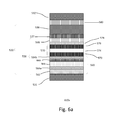
- FIG. 6 b shows a cross-sectional view of another embodiment of a magnetic storage unit 610 b of a magnetic memory cell.
- the storage unit includes a bottom pinned pMTJ stack or element 520 disposed between bottom and top electrodes 531 and 532 .
- the pMTJ element is similar to that described in FIGS. 5 a -5 b and 6 a . Common elements may not be described or described in detail.
- the pMTJ element includes a fixed layer 526 , a free layer 528 , and a tunneling barrier layer disposed between the fixed layer and the free layer.
- the fixed layer is disposed below the free layer, forming the bottom pinned pMTJ element.
- a capping layer 580 is disposed over the free layer. The fixed layer, tunneling barrier layer, and free layer form the pMTJ element 520 .
- the pMTJ element 610 b of FIG. 6 b includes first and second tunneling barrier layers 527 a and 527 b .
- This configuration produces a dual tunneling barrier pMTJ element.
- the free layer 528 is disposed between the first and second tunneling barrier layers 527 a - 527 b .
- the tunneling barrier layers may be MgO tunneling barrier layers. Other suitable types of tunneling barrier layers may also be useful. It is also understood that the tunneling barrier layers need not be the same. As for the other layers of the MTJ element, they are the same or similar.
- the various layers of the pMTJ stack may be disposed on a dielectric layer of BEOL process.
- the various layers of the pMTJ stack may be disposed on a metal level with the bottom electrode.
- they are patterned to form the pMTJ stack. Patterning may be achieved using, for example, mask and etch techniques. Such technique may include forming a patterned photoresist mask over the top of the stack and etching the layers of the MTJ stack using, for example, an anisotropic etch such as a reactive ion etch (RIE). The process may continue to form top electrode as well as other ILD levels of the BEOL process.
- RIE reactive ion etch
- FIGS. 7 a -7 l show cross-sectional views of an embodiment of a process 700 for forming a device.
- the process includes forming a memory cell.
- the memory cell for example, may be a magnetic random access memory (MRAM) cell.
- MRAM magnetic random access memory
- the memory cell for example, is the same or similar to that described in FIG. 2 and includes an MTJ element as described in FIGS. 5 a -5 b and FIGS. 6 a -6 b . Common elements may not be described or described in detail.
- the cross-sectional views are along the bit line direction.
- the cross-sectional views show one memory cell, it is understood that the device includes a plurality of memory cells of, for example, a memory array.
- the process of forming the cell is highly compatible with CMOS logic process.
- the cell can be formed simultaneously with CMOS logic devices (not shown) on the same substrate.
- a substrate 705 is provided.
- the substrate for example, is a semiconductor substrate, such as a silicon substrate.
- the substrate may be a lightly doped p-type substrate. Providing an intrinsic or other types of doped substrates, such as silicon germanium (SiGe), germanium (Ge), gallium arsenide (GaAs) or any other suitable semiconductor materials, may also be useful.
- the substrate may be a crystalline-on-insulator (COI) substrate.
- a COI substrate includes a surface crystalline layer separated from a bulk crystalline by an insulator layer.
- the insulator layer for example, may be formed of a dielectric insulating material.
- the insulator layer for example, includes silicon oxide, which provides a buried oxide (BOX) layer. Other types of dielectric insulating materials may also be useful.
- the COI substrate for example, is a silicon-on-insulator (SOI) substrate.
- SOI silicon-on-insulator
- the surface and bulk crystalline layers are single crystalline silicon. Other types of COI substrates may also be useful. It is understood that the surface and bulk layers need not be formed of the same material.
- the substrate is processed to define a cell region in which a memory cell is formed.
- the cell region may be part of an array region.
- the array region may include a plurality of cell regions.
- the substrate may include other types of device regions, such as a logic region. Other types of regions may also be provided.
- Isolation regions 780 are formed in the substrate.
- the isolation regions are shallow trench isolation (STI) regions. Other types of isolation regions may also be useful.
- the isolation regions are provided to isolate device regions from other regions.
- the isolation regions may also isolate contact regions within a cell region. Isolation regions may be formed by, for example, etching trenches in the substrate and filling them with a dielectric material, such as silicon oxide.
- a planarization process such as chemical mechanical polish (CMP), is performed to remove excess dielectric material, leaving, for example, STI regions isolating the device regions.
- CMP chemical mechanical polish
- a doped well or device well 708 is formed.
- the well for example, is formed after the isolation regions.
- the well serves as a well for the select transistor of the selector unit.
- the well for example, is a second polarity type doped well.
- the second polarity type is the opposite polarity type of the transistor of the cell selector unit.
- the device well is a p-type well for a n-type cell select transistor, such as a metal oxide semiconductor field effect transistor (MOSFET).
- MOSFET metal oxide semiconductor field effect transistor
- an implant mask may be employed to implant the dopants to form the doped well.
- the implant mask for example, is a patterned photoresist layer.
- the implant mask exposes regions of the substrate in which the second polarity wells are formed.
- the device well may be lightly or intermediately doped with second polarity type dopants.
- the device well may have a dopant concentration of about 1E15 to 1E19/cm 3 . Other dopant concentrations may also be useful.
- the well for example, may be a common device well for the array.
- the process may include forming other wells for other device regions.
- the wells are different polarity type of dopant concentration, they may be formed using separate processes, such as separate mask and implants.
- first polarity typed doped wells, wells of different dopant concentrations as well as other wells may be formed using separate mask and implant processes.
- gate layers are formed on the substrate.
- the gate layers include a gate dielectric layer 742 and a gate electrode layer 743 thereover.
- the gate dielectric layer for example, may be a silicon oxide layer.
- the gate dielectric may be formed by thermal oxidation.
- As for the gate electrode layer it may be a polysilicon layer.
- the gate electrode layer may be formed by chemical vapor deposition (CVD).
- CVD chemical vapor deposition
- Other suitable types of gate layers, including high k dielectric and metal gate electrode layers, or other suitable techniques for forming gate layers may also be useful.
- the gate layers are patterned to form a gate 744 of the select transistor of the select unit.
- Patterning the gate layers may be achieved using mask and etch techniques. For example, a soft mask, such as photoresist may be formed over the gate electrode layer. An exposure source may selectively expose the photoresist layer through a reticle containing the desired pattern. After selectively exposing the photoresist layer, it is developed to form openings corresponding to locations where the gate layers are to be removed. To improve lithographic resolution, an anti-reflective coating may be used below the photoresist layer. The patterned mask layer is used to pattern the gate layers.
- an anisotropic etch such as reactive ion etch (RIE) is used to remove exposed portions of the gate layers.
- RIE reactive ion etch
- Other types of etch processes may also be useful.
- the etch transfers the pattern of the mask layer to the underlying gate layers. Patterning the gate layers forms gate of the select transistor.
- the gate for example, may be gate conductor along a first or word line direction.
- a gate conductor forms a common gate for a row of memory cells. It is understood that gates of the memory cells of the array may be formed.
- an implant is performed to first and second S/D regions 745 and 746 on sides of the gate.
- the implant for example, implant first polarity type dopants to form first polarity type S/D regions.
- An implant mask (not shown) may be used to form the first polarity type S/D regions in the substrate.
- the implant forms heavily doped first polarity type S/D regions in the substrate adjacent to the gates.
- the first polarity type dopants for example, include n-type dopants.
- the implantation process to form the first polarity type S/D regions may be performed together while forming first polarity type S/D regions in other device regions (not shown) on the same substrate as well as first polarity type contact regions.
- the S/D regions for example, include dopant concentration of about 5E19 to 1E21/cm 3 . Other dopant concentration may also be useful.
- An LD extension implant may be performed to form LD extension regions (not shown) of the S/D regions.
- the LD extension implant may be performed prior to forming the S/D regions.
- An implant mask may be used to form the LD extension regions.
- first polarity type dopants are implanted into the substrate.
- the first polarity type dopants for example, include n-type dopants.
- the implant forms LD extension regions in the substrate adjacent to the gates.
- the LD extension regions extend slightly under the gates and are typically shallower than the S/D regions.
- the LD extension regions for example, include dopant concentration of about 1E18 to 5E19/cm 3 . Other dopant concentration may also be useful.
- a halo region may also be formed.
- the halo region may be formed at the same time as the LD extension region.
- sidewall spacers (not shown) may be formed on sidewalls of the gate followed by forming the S/D regions.
- second polarity type S/D and extension regions may be performed.
- the second polarity type implants form S/D and extension regions for second polarity type transistors in other device regions as well as second polarity type contact regions.
- a dielectric layer 790 1 is formed on the substrate, covering the transistors.
- the dielectric layer for example, serves as a dielectric layer of an ILD layer.
- the dielectric layer serves as a PMD or CA level of an ILD layer.
- the dielectric layer for example, is a silicon oxide layer. Other types of dielectric layers may also be useful.
- the dielectric layer may be formed by CVD. Other techniques for forming the dielectric layer may also be useful.
- a planarizing process may be performed to produce a planar surface.
- the planarizing process for example, may include CMP. Other types of planarizing processes may also be useful.
- contacts 793 are formed in the dielectric layer 790 1 as shown in FIG. 7 f .
- the contacts for example, connect to contact regions, such as S/D regions and gate (not shown).
- Forming the contacts may include forming contact vias in the dielectric layer to expose the contact regions. Forming the contact vias may be achieved using mask and etch techniques.
- a conductive material is deposited to fill the vias.
- the conductive material for example, may be tungsten. Other types of conductive materials may also be useful.
- a planarization process, such as CMP, is performed to remove excess conductive material, leaving contact plugs in the contact vias.
- a dielectric layer 790 2 is formed over the substrate, covering the lower dielectric layer 790 1 .
- the dielectric layer for example, serves as a metal level of an ILD layer. In one embodiment, the dielectric layer serves as M 1 level of the ILD layer.
- the dielectric layer for example, is a silicon oxide layer. Other types of dielectric layers may also be useful.
- the dielectric layer may be formed by CVD. Other techniques for forming the dielectric layer may also be useful. Since the underlying surface is already planar, a planarizing process may not be needed. However, it is understood that a planarization process, such as CMP, may be performed if desired to produce a planar surface.
- conductive or metal lines 795 are formed in the dielectric layer 790 2 .
- the conductive lines may be formed by damascene technique.
- the upper dielectric layer may be etched to form trenches or openings using, for example, mask and etch techniques.
- a conductive layer is formed on the substrate, filling the openings.
- a copper or copper alloy layer may be formed to fill the openings.
- the conductive material may be formed by, for example, plating, such as electro or electroless plating. Other types of conductive layers or forming techniques may also be useful.
- a source line SL is formed to connect to the source region 746 of the transistor while other interconnects, such as interconnect pad 797 formed in M 1 is coupled to the drain region 745 .
- the SL may be along the wordline direction. Providing SL in the bitline direction may also be useful.
- the interconnect pad it may serve as a storage pad. Other conductive lines and pads may also be formed.
- the process continues to form a storage unit of the memory cell.
- the process forms various layers 712 of a storage unit with a pMTJ element.
- the various layers are formed on the dielectric layer 790 2 .
- the layers may include layers as described in FIG. 5 a , 5 b , 6 a or 6 b .
- the layers may be formed by PVD or other suitable deposition techniques. The deposition technique may depend on the type of layer.
- the layers are patterned to form a storage unit 710 with a pMTJ element, as shown in FIG. 7 j . Patterning the layers may be achieved using an anisotropic etch, such as RIE, with a patterned mask layer. Other techniques for forming the MTJ element may also be useful.
- a storage dielectric layer 7903 is formed over the MTJ storage unit.
- the dielectric layer covers the storage unit 710 .
- the storage dielectric layer for example, is a silicon oxide layer.
- the storage dielectric layer may be formed by, for example, CVD. Other types of storage dielectric layers or forming techniques may also be useful.
- a planarization process is performed to remove excess dielectric material to form a planar surface.
- the planarization process for example, is CMP.
- the storage dielectric layer is disposed above the surface of the storage unit.
- the storage dielectric layer includes V 1 and M 1 levels.
- a conductive or metal line is formed in the dielectric layer in M 2 .
- a bitline BL is formed in M 2 of the dielectric layer, coupling to the storage unit.
- Other metal lines may also be formed.
- the metal lines in M 2 may be formed using a dual damascene technique.
- Additional processes may be performed to complete forming the device.
- the processes may include forming additional ILD levels, pad level, passivation level, pad opening, dicing, assembly and testing. Other types of processes may also be performed.
- the storage unit is formed in V 1 and BL is formed in M 2 .
- Forming the storage unit and BL in other ILD levels, such as in an upper ILD level, may also be useful.
- contact and interconnect pads may be formed in the intermediate ILD levels to connect to the storage unit.
- the contact and interconnect pads may be formed using dual damascene techniques.
- a metal wordline may be provided in a metal layer above the gate.
- the metal wordline for example, may be coupled to the gate of the select transistor.
- the metal wordline may be provided in M 1 or other metal levels.
- the metal wordline may be parallel with the SL.
- the various components are disposed in specific via or metal levels. It is understood that other configurations of the memory cell may also be useful. For example, the components may be disposed in other metal or via levels.
- the embodiments as described result in various advantages.
- the provision of the base layer having the seed layer with roughness smoother or crystallinity enhancing layer and wetting layer enhances the FCC structure along the (111) orientation of the fixed layer, thereby improving PMA of the fixed layer.
- the seed layer as described in this disclosure includes a reduced thickness without sacrificing PMA of the fixed layer.
- a thinner seed layer reduces total interface or surface roughness of the fixed layer.
- the reduced interface roughness improves thermal endurance of the pMTJ stack, for example at about 400° C.
- a pMTJ stack with improved thermal budget and PMA can be achieved.
- the seed layer with reduced thickness could also lead to a minimized pMTJ stack.
- the process as described is highly compatible with logic processing or technology. This avoids investment of new tools and does not require creating new low temperature modules or processing, providing a cost effective solution.
Landscapes
- Engineering & Computer Science (AREA)
- Manufacturing & Machinery (AREA)
- Mram Or Spin Memory Techniques (AREA)
- Semiconductor Memories (AREA)
Abstract
Description
Claims (20)
Priority Applications (1)
| Application Number | Priority Date | Filing Date | Title |
|---|---|---|---|
| US15/057,107 US9842989B2 (en) | 2015-02-27 | 2016-02-29 | Magnetic memory with high thermal budget |
Applications Claiming Priority (3)
| Application Number | Priority Date | Filing Date | Title |
|---|---|---|---|
| US201562121494P | 2015-02-27 | 2015-02-27 | |
| US201562135720P | 2015-03-20 | 2015-03-20 | |
| US15/057,107 US9842989B2 (en) | 2015-02-27 | 2016-02-29 | Magnetic memory with high thermal budget |
Publications (2)
| Publication Number | Publication Date |
|---|---|
| US20160254444A1 US20160254444A1 (en) | 2016-09-01 |
| US9842989B2 true US9842989B2 (en) | 2017-12-12 |
Family
ID=56799140
Family Applications (2)
| Application Number | Title | Priority Date | Filing Date |
|---|---|---|---|
| US15/057,109 Active 2036-04-02 US9972774B2 (en) | 2015-02-27 | 2016-02-29 | Magnetic memory with high thermal budget |
| US15/057,107 Expired - Fee Related US9842989B2 (en) | 2015-02-27 | 2016-02-29 | Magnetic memory with high thermal budget |
Family Applications Before (1)
| Application Number | Title | Priority Date | Filing Date |
|---|---|---|---|
| US15/057,109 Active 2036-04-02 US9972774B2 (en) | 2015-02-27 | 2016-02-29 | Magnetic memory with high thermal budget |
Country Status (1)
| Country | Link |
|---|---|
| US (2) | US9972774B2 (en) |
Families Citing this family (21)
| Publication number | Priority date | Publication date | Assignee | Title |
|---|---|---|---|---|
| US9240547B2 (en) | 2013-09-10 | 2016-01-19 | Micron Technology, Inc. | Magnetic tunnel junctions and methods of forming magnetic tunnel junctions |
| US9666640B2 (en) * | 2015-03-16 | 2017-05-30 | Globalfoundries Singapore Pte. Ltd. | High thermal budget magnetic memory |
| US10128309B2 (en) | 2015-03-27 | 2018-11-13 | Globalfoundries Singapore Pte. Ltd. | Storage layer for magnetic memory with high thermal stability |
| US9502642B2 (en) | 2015-04-10 | 2016-11-22 | Micron Technology, Inc. | Magnetic tunnel junctions, methods used while forming magnetic tunnel junctions, and methods of forming magnetic tunnel junctions |
| US9960346B2 (en) | 2015-05-07 | 2018-05-01 | Micron Technology, Inc. | Magnetic tunnel junctions |
| US9627529B1 (en) * | 2015-05-21 | 2017-04-18 | Altera Corporation | Well-tap structures for analog matching transistor arrays |
| CN107636851B (en) * | 2015-06-26 | 2022-02-01 | 英特尔公司 | Perpendicular magnetic memory with symmetric fixed layer |
| US10297745B2 (en) | 2015-11-02 | 2019-05-21 | Globalfoundries Singapore Pte. Ltd. | Composite spacer layer for magnetoresistive memory |
| US9680089B1 (en) * | 2016-05-13 | 2017-06-13 | Micron Technology, Inc. | Magnetic tunnel junctions |
| CN110024150A (en) * | 2016-12-30 | 2019-07-16 | 英特尔公司 | Erect spin transfer torque memory (pSTTM) device with enhancing stability and forming method thereof |
| KR102449605B1 (en) | 2017-06-05 | 2022-10-04 | 삼성전자주식회사 | Semiconductor device and method for manufacturing the same |
| US10256398B2 (en) * | 2017-06-28 | 2019-04-09 | Globalfoundries Singapore Pte. Ltd. | Magnetic random access memory structures, integrated circuits, and methods for fabricating the same |
| US20190066746A1 (en) * | 2017-08-28 | 2019-02-28 | Qualcomm Incorporated | VARYING ENERGY BARRIERS OF MAGNETIC TUNNEL JUNCTIONS (MTJs) IN DIFFERENT MAGNETO-RESISTIVE RANDOM ACCESS MEMORY (MRAM) ARRAYS IN A SEMICONDUCTOR DIE TO FACILITATE USE OF MRAM FOR DIFFERENT MEMORY APPLICATIONS |
| US20190304521A1 (en) * | 2018-03-28 | 2019-10-03 | Globalfoundries Singapore Pte. Ltd. | Magnetic random access memory structures, integrated circuits, and methods for fabricating the same |
| WO2020041582A1 (en) * | 2018-08-23 | 2020-02-27 | Everspin Technologies, Inc. | Magnetoresistive stack device fabrication methods |
| WO2020106552A1 (en) * | 2018-11-19 | 2020-05-28 | Everspin Technologies, Inc. | Magnetoresistive stack with seed region and method of manufacturing the same |
| CN112736191A (en) * | 2019-10-14 | 2021-04-30 | 上海磁宇信息科技有限公司 | Magnetic tunnel junction structure with symmetrical structure and magnetic random access memory |
| CN112864306A (en) * | 2019-11-12 | 2021-05-28 | 上海磁宇信息科技有限公司 | Magnetic tunnel junction structure with symmetrical double barrier layers and magnetic random access memory |
| US11302372B2 (en) * | 2020-02-07 | 2022-04-12 | International Business Machines Corporation | MTJ stack containing a top magnetic pinned layer having strong perpendicular magnetic anisotropy |
| US11698423B2 (en) * | 2020-08-12 | 2023-07-11 | Taiwan Semiconductor Manufacturing Co., Ltd. | Magnetic tunnel junction device and method |
| TWI797817B (en) * | 2021-11-08 | 2023-04-01 | 志陽憶存股份有限公司 | Memory device and method of manufacturing the same |
Citations (16)
| Publication number | Priority date | Publication date | Assignee | Title |
|---|---|---|---|---|
| US20040174740A1 (en) * | 2003-03-03 | 2004-09-09 | Kyu-Mann Lee | Magnetic tunnel junction structures and methods of fabrication |
| US6960480B1 (en) * | 2004-05-19 | 2005-11-01 | Headway Technologies, Inc. | Method of forming a magnetic tunneling junction (MTJ) MRAM device and a tunneling magnetoresistive (TMR) read head |
| US20110014500A1 (en) * | 2009-07-17 | 2011-01-20 | Maglc Technologies, Inc. | Structure and method to fabricate high performance MTJ devices for spin-transfer torque (STT)-RAM application |
| US20110293967A1 (en) * | 2010-05-28 | 2011-12-01 | Headway Technologies, Inc. | Multilayer structure with high perpendicular anisotropy for device applications |
| US20120292724A1 (en) * | 2011-05-19 | 2012-11-22 | Woo-Chang Lim | Magnetic device |
| US20130075837A1 (en) * | 2011-09-22 | 2013-03-28 | Taiwan Semiconductor Manufacturing Company, Ltd. | Technique for smoothing an interface between layers of a semiconductor device |
| US20140070341A1 (en) * | 2012-09-11 | 2014-03-13 | Headway Technologies, Inc. | Minimal Thickness Synthetic Antiferromagnetic (SAF) Structure with Perpendicular Magnetic Anisotropy for STT-MRAM |
| US20140103469A1 (en) * | 2012-10-11 | 2014-04-17 | Headway Technologies, Inc. | Seed Layer for Multilayer Magnetic Materials |
| US20140145792A1 (en) * | 2012-11-27 | 2014-05-29 | Headway Technologies, Inc. | Free Layer with Out-of-Plane Anisotropy for Magnetic Device Applications |
| US20140197504A1 (en) * | 2013-01-11 | 2014-07-17 | Headway Technologies, Inc. | Mg Discontinuous Insertion Layer for Improving MTJ Shunt |
| US20140306302A1 (en) * | 2013-04-16 | 2014-10-16 | Headway Technologies, Inc. | Fully Compensated Synthetic Antiferromagnet for Spintronics Applications |
| US20150008547A1 (en) * | 2013-07-05 | 2015-01-08 | Headway Technologies, Inc. | Hybridized Oxide Capping Layer for Perpendicular Magnetic Anisotropy |
| US20150008550A1 (en) * | 2013-06-17 | 2015-01-08 | Imec | Magnetic memory element |
| US20150061058A1 (en) * | 2011-05-10 | 2015-03-05 | Headway Technologies, Inc. | Co/Ni Multilayers with Improved Out-of-Plane Anisotropy for Magnetic Device Applications |
| US20150171316A1 (en) * | 2013-12-17 | 2015-06-18 | Qualcomm Incorporated | Hybrid synthetic antiferromagnetic layer for perpendicular magnetic tunnel junction (mtj) |
| US20160043309A1 (en) * | 2014-04-09 | 2016-02-11 | International Business Machines Corporation | Multibit self-reference thermally assisted mram |
Family Cites Families (1)
| Publication number | Priority date | Publication date | Assignee | Title |
|---|---|---|---|---|
| US8922956B2 (en) * | 2010-06-04 | 2014-12-30 | Seagate Technology Llc | Tunneling magneto-resistive sensors with buffer layers |
-
2016
- 2016-02-29 US US15/057,109 patent/US9972774B2/en active Active
- 2016-02-29 US US15/057,107 patent/US9842989B2/en not_active Expired - Fee Related
Patent Citations (16)
| Publication number | Priority date | Publication date | Assignee | Title |
|---|---|---|---|---|
| US20040174740A1 (en) * | 2003-03-03 | 2004-09-09 | Kyu-Mann Lee | Magnetic tunnel junction structures and methods of fabrication |
| US6960480B1 (en) * | 2004-05-19 | 2005-11-01 | Headway Technologies, Inc. | Method of forming a magnetic tunneling junction (MTJ) MRAM device and a tunneling magnetoresistive (TMR) read head |
| US20110014500A1 (en) * | 2009-07-17 | 2011-01-20 | Maglc Technologies, Inc. | Structure and method to fabricate high performance MTJ devices for spin-transfer torque (STT)-RAM application |
| US20110293967A1 (en) * | 2010-05-28 | 2011-12-01 | Headway Technologies, Inc. | Multilayer structure with high perpendicular anisotropy for device applications |
| US20150061058A1 (en) * | 2011-05-10 | 2015-03-05 | Headway Technologies, Inc. | Co/Ni Multilayers with Improved Out-of-Plane Anisotropy for Magnetic Device Applications |
| US20120292724A1 (en) * | 2011-05-19 | 2012-11-22 | Woo-Chang Lim | Magnetic device |
| US20130075837A1 (en) * | 2011-09-22 | 2013-03-28 | Taiwan Semiconductor Manufacturing Company, Ltd. | Technique for smoothing an interface between layers of a semiconductor device |
| US20140070341A1 (en) * | 2012-09-11 | 2014-03-13 | Headway Technologies, Inc. | Minimal Thickness Synthetic Antiferromagnetic (SAF) Structure with Perpendicular Magnetic Anisotropy for STT-MRAM |
| US20140103469A1 (en) * | 2012-10-11 | 2014-04-17 | Headway Technologies, Inc. | Seed Layer for Multilayer Magnetic Materials |
| US20140145792A1 (en) * | 2012-11-27 | 2014-05-29 | Headway Technologies, Inc. | Free Layer with Out-of-Plane Anisotropy for Magnetic Device Applications |
| US20140197504A1 (en) * | 2013-01-11 | 2014-07-17 | Headway Technologies, Inc. | Mg Discontinuous Insertion Layer for Improving MTJ Shunt |
| US20140306302A1 (en) * | 2013-04-16 | 2014-10-16 | Headway Technologies, Inc. | Fully Compensated Synthetic Antiferromagnet for Spintronics Applications |
| US20150008550A1 (en) * | 2013-06-17 | 2015-01-08 | Imec | Magnetic memory element |
| US20150008547A1 (en) * | 2013-07-05 | 2015-01-08 | Headway Technologies, Inc. | Hybridized Oxide Capping Layer for Perpendicular Magnetic Anisotropy |
| US20150171316A1 (en) * | 2013-12-17 | 2015-06-18 | Qualcomm Incorporated | Hybrid synthetic antiferromagnetic layer for perpendicular magnetic tunnel junction (mtj) |
| US20160043309A1 (en) * | 2014-04-09 | 2016-02-11 | International Business Machines Corporation | Multibit self-reference thermally assisted mram |
Non-Patent Citations (2)
| Title |
|---|
| H. Kurt et al., Enhanced perpendicular magnetic anisotropy in Co/Ni multilayers with a thin seed layer, Journal of Applied Physics 108, Oct. 7, 2010, pp. 073916-1-073916-4, 108-073916, AIP Publishing, Melville, NY. |
| Long You et. al., Co/Ni multilayers with perpendicular anisotropy for spintronic device applications, Applied Physics Letters 100, Apr. 26, 2012, pp. 172411-1-172411-4, 100-172411, AIP Publishing, Melville, NY. |
Also Published As
| Publication number | Publication date |
|---|---|
| US20160254445A1 (en) | 2016-09-01 |
| US9972774B2 (en) | 2018-05-15 |
| US20160254444A1 (en) | 2016-09-01 |
Similar Documents
| Publication | Publication Date | Title |
|---|---|---|
| US9842989B2 (en) | Magnetic memory with high thermal budget | |
| US10840297B2 (en) | Storage layer for magnetic memory with high thermal stability | |
| US10297745B2 (en) | Composite spacer layer for magnetoresistive memory | |
| US20160276580A1 (en) | Bottom electrode for magnetic memory to increase tmr and thermal budget | |
| US9865649B2 (en) | Integrated two-terminal device and logic device with compact interconnects having shallow via for embedded application | |
| US10121964B2 (en) | Integrated magnetic random access memory with logic device | |
| US9698200B2 (en) | Magnetism-controllable dummy structures in memory device | |
| US10529917B2 (en) | High energy barrier perpendicular magnetic tunnel junction element with reduced temperature sensitivity | |
| US9570138B2 (en) | Magnetic memory cells with fast read/write speed | |
| US20180130943A1 (en) | Magnetic tunnel junction element with reduced temperature sensitivity | |
| US10446607B2 (en) | Integrated two-terminal device with logic device for embedded application | |
| US9734882B2 (en) | Magnetic memory cells with high write current and read stability | |
| US9882125B2 (en) | Selector device for a non-volatile memory cell | |
| US10283246B1 (en) | MTJ structures, STT MRAM structures, and methods for fabricating integrated circuits including the same | |
| US10516096B2 (en) | Magnetic random access memory structures, integrated circuits, and methods for fabricating the same | |
| US10256398B2 (en) | Magnetic random access memory structures, integrated circuits, and methods for fabricating the same | |
| US9876163B2 (en) | Magnetic memory with tunneling magnetoresistance enhanced spacer layer | |
| US10468457B1 (en) | Magnetic random access memory structures and integrated circuits with cobalt anti-parallel layers, and methods for fabricating the same | |
| US10446205B1 (en) | Magnetic random access memory structures, integrated circuits, and methods for fabricating the same | |
| US10483121B2 (en) | Embedded memory in back-end-of-line low-k dielectric | |
| US9666640B2 (en) | High thermal budget magnetic memory | |
| US9343662B2 (en) | Magnetic memory device and method of forming thereof | |
| US20190304521A1 (en) | Magnetic random access memory structures, integrated circuits, and methods for fabricating the same | |
| US20230299042A1 (en) | Memory Device and Method of Forming The Same |
Legal Events
| Date | Code | Title | Description |
|---|---|---|---|
| AS | Assignment |
Owner name: GLOBALFOUNDRIES SINGAPORE PTE. LTD., SINGAPORE Free format text: ASSIGNMENT OF ASSIGNORS INTEREST;ASSIGNORS:TAHMASEBI, TAIEBEH;GAN, KAH WEE;SEET, CHIM SENG;REEL/FRAME:037856/0308 Effective date: 20160229 |
|
| STCF | Information on status: patent grant |
Free format text: PATENTED CASE |
|
| AS | Assignment |
Owner name: WILMINGTON TRUST, NATIONAL ASSOCIATION, DELAWARE Free format text: SECURITY AGREEMENT;ASSIGNOR:GLOBALFOUNDRIES SINGAPORE PTE. LTD.;REEL/FRAME:047660/0203 Effective date: 20181127 |
|
| AS | Assignment |
Owner name: GLOBALFOUNDRIES SINGAPORE PTE. LTD., SINGAPORE Free format text: RELEASE BY SECURED PARTY;ASSIGNOR:WILMINGTON TRUST, NATIONAL ASSOCIATION;REEL/FRAME:054481/0673 Effective date: 20201117 |
|
| MAFP | Maintenance fee payment |
Free format text: PAYMENT OF MAINTENANCE FEE, 4TH YEAR, LARGE ENTITY (ORIGINAL EVENT CODE: M1551); ENTITY STATUS OF PATENT OWNER: LARGE ENTITY Year of fee payment: 4 |
|
| FEPP | Fee payment procedure |
Free format text: MAINTENANCE FEE REMINDER MAILED (ORIGINAL EVENT CODE: REM.); ENTITY STATUS OF PATENT OWNER: LARGE ENTITY |
|
| LAPS | Lapse for failure to pay maintenance fees |
Free format text: PATENT EXPIRED FOR FAILURE TO PAY MAINTENANCE FEES (ORIGINAL EVENT CODE: EXP.); ENTITY STATUS OF PATENT OWNER: LARGE ENTITY |
|
| STCH | Information on status: patent discontinuation |
Free format text: PATENT EXPIRED DUE TO NONPAYMENT OF MAINTENANCE FEES UNDER 37 CFR 1.362 |
|
| FP | Lapsed due to failure to pay maintenance fee |
Effective date: 20251212 |