US9842179B2 - Recording medium, ranking method, and information processing device - Google Patents
Recording medium, ranking method, and information processing device Download PDFInfo
- Publication number
- US9842179B2 US9842179B2 US15/001,310 US201615001310A US9842179B2 US 9842179 B2 US9842179 B2 US 9842179B2 US 201615001310 A US201615001310 A US 201615001310A US 9842179 B2 US9842179 B2 US 9842179B2
- Authority
- US
- United States
- Prior art keywords
- ibis
- characteristic
- characteristic models
- margin
- models
- Prior art date
- Legal status (The legal status is an assumption and is not a legal conclusion. Google has not performed a legal analysis and makes no representation as to the accuracy of the status listed.)
- Expired - Fee Related
Links
Images


Classifications
-
- G06F17/5036—
-
- G—PHYSICS
- G06—COMPUTING OR CALCULATING; COUNTING
- G06F—ELECTRIC DIGITAL DATA PROCESSING
- G06F30/00—Computer-aided design [CAD]
- G06F30/30—Circuit design
- G06F30/36—Circuit design at the analogue level
- G06F30/367—Design verification, e.g. using simulation, simulation program with integrated circuit emphasis [SPICE], direct methods or relaxation methods
Definitions
- the embodiments discussed herein are related to a recording medium, a ranking method, and an information processing device.
- IBIS I/O Buffer Information Specification
- a user verifies an action of a semiconductor component by observing a waveform of a signal propagated through a transmission line obtained by a transmission line simulation.
- the semiconductor component include an Integrated Circuit (IC) and a Large-Scale Integration (LSI).
- the IC or LSI may be a semiconductor memory such as a Dynamic Random Access Memory (DRAM), a Static Random Access Memory (SRAM), or a flash memory.
- the IC or LSI may be a Central Processing Unit (CPU), a multicore CPU, a Field Programmable Gate Array (FPGA), or a Programmable Logic Device (PLD).
- CPU Central Processing Unit
- FPGA Field Programmable Gate Array
- PLD Programmable Logic Device
- a simulation device simulates a transmission line by using each of the plurality of IBIS models so as to determine waveform quality and obtain delay data.
- a simulation device simulates a transmission line by using each of the plurality of IBIS models so as to determine waveform quality and obtain delay data.
- a user desires to select an element of an IBIS model having a large margin for evaluation items as an element to be loaded onto a product in order to obtain a produce having fewer malfunctions.
- a non-transitory computer-readable recording medium having stored therein a program for causing a computer to execute a process.
- the process includes: generating a second characteristic model from a plurality of first characteristic models by using a maximum value and a minimum value from among maximum values and minimum values of a prescribed parameter in the respective plurality of first characteristic models, the plurality of first characteristic models respectively describing electric characteristics of a plurality of semiconductor components; executing simulation by using the second characteristic model; calculating a plurality of first margins for an evaluation item according to a result of the simulation; calculating a plurality of second margins for the evaluation item with respect to each of the first characteristic models by using a maximum value and a minimum value of the prescribed parameter in each of the plurality of first characteristic models; calculating a ratio of each of the plurality of second margins to a maximum margin of the plurality of first margins; and ranking the plurality of first characteristic models according to the ratio.
- FIG. 1 illustrates a configuration of a simulation device according to an embodiment.
- FIG. 2 illustrates information relating to input IBIS models.
- FIG. 3 illustrates the description content of an IBIS model.
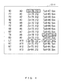
- FIG. 4 illustrates characteristic impedances and propagation delay times that correspond to respective signal lines.
- FIG. 5 illustrates the description content of an IBIS model.
- FIG. 6 illustrates characteristic impedances and propagation delay times that correspond to respective signal lines.
- FIG. 7 illustrates the description content of an IBIS model.
- FIG. 8 illustrates characteristic impedances and propagation delay times that correspond to respective signal lines.
- FIG. 9 illustrates a maximum value and a minimum value of each parameter in each of the IBIS models.
- FIG. 10 illustrates a maximum value and a minimum value of each parameter in a plurality of IBIS models.
- FIG. 11 illustrates the description content of an IBIS model for verification.
- FIG. 12A is a flowchart of a ranking process according to an embodiment.
- FIG. 12B is a flowchart of a ranking process according to an embodiment.
- FIG. 12C is a flowchart of a ranking process according to an embodiment.
- FIG. 13 illustrates a list of conditions used in a simulation.
- FIG. 14 illustrates a topology-based simulation of a transmission line.
- FIG. 15 illustrates a voltage waveform of each unit.
- FIG. 16 is an enlarged view of a broken-line portion in FIG. 15 .
- FIG. 17 is a table describing values of evaluation items under respective simulation conditions.
- FIG. 18 is a table describing margin values for evaluation items under respective simulation conditions.
- FIG. 19A is a margin value characteristic table and graph relating to an item of interest (1) and a margin value for an evaluation item (1).
- FIG. 19B is a margin value characteristic table and graph relating to an item of interest (1) and a margin value for an evaluation item (2).
- FIG. 19C is a margin value characteristic table and graph relating to an item of interest (1) and a margin value for an evaluation item (3).
- FIG. 20A is a margin value characteristic table and graph relating to an item of interest (2) and a margin value for an evaluation item (1).
- FIG. 20B is a margin value characteristic table and graph relating to an item of interest (2) and a margin value for an evaluation item (2).
- FIG. 20C is a margin value characteristic table and graph relating to an item of interest (2) and a margin value for an evaluation item (3).
- FIG. 21A is a margin value characteristic table and graph relating to an item of interest (3) and a margin value for an evaluation item (1).
- FIG. 21B is a margin value characteristic table and graph relating to an item of interest (3) and a margin value for an evaluation item (2).
- FIG. 21C is a margin value characteristic table and graph relating to an item of interest (3) and a margin value for an evaluation item (3).
- FIG. 22 is a flowchart illustrating details of a process of calculating a margin value used for a determination point according to an embodiment.
- FIG. 23 is a diagram explaining a method for calculating a margin value used for a determination point.
- FIG. 24 illustrates a margin value, used for a determination point under each condition.
- FIG. 25 illustrates a determination point under each condition.
- FIG. 26 illustrates the total of determination points and a rank of each IBIS model.
- FIG. 27 illustrates a configuration of an information processing device (computer).
- FIG. 1 illustrates a configuration of a simulation device according to an embodiment.
- a simulation device 1 includes a processing unit 10 , a storage 20 , and an input/output unit 30 .
- the simulation device 1 is, for example, a computer such as a personal computer (PC) or a server.
- the simulation device 1 is an example of an information processing device.
- the processing unit 10 includes a specifying unit 11 , a generating unit 12 , an executing unit 13 , a calculating unit 14 , and a ranking unit 15 .
- the storage 20 may store a plurality of IBIS models for verification 22 .
- the IBIS model 21 - i is, for example, an IBIS model input into the simulation device 1 via an input unit 31 .
- the IBIS model 21 - i is an example of the first characteristic model.
- the IBIS model for verification 22 is, for example, an IBIS model for verification generated by the generating unit 12 in the generating process described later.
- the IBIS model for verification 22 is an example of the second characteristic model.
- the input/output unit 30 includes an input unit 31 and an output unit 32 .
- the specifying unit 11 specifies the first signal line for which a prescribed parameter has a maximum value, and the second signal line for which the prescribed parameter has a minimum value in the IBIS model 21 - i describing electric characteristics for respective plural signal lines of a semiconductor component.
- the signal line refers, for example, to a wiring from a pin to a die pad in a package included in a semiconductor component.
- Examples of the electric characteristic of a signal line include a resistance value of the signal line, a capacitance value of the signal line, and an inductance value of the signal line.
- the prescribed parameter of the signal line may be, for example, a characteristic impedance of the signal line.
- the specifying unit 11 obtains a characteristic impedance Z 0 for each of the plural signal lines by using a capacitance value C and an inductance value L according to the following expression (1).
- Z 0 ⁇ ( L/C ) (1)
- the prescribed parameter of the signal line may be, for example, a propagation delay time of a signal propagated through the signal line.
- the specifying unit 11 obtains a propagation delay time Tpd for each of the plural signal lines by using a capacitance value C and an inductance value L according to the following expression (2).
- Tpd ⁇ ( L/C ) (2)
- the specifying unit 11 specifies the first signal line for which a prescribed parameter has a maximum value, and the second signal line for which the prescribed parameter has a minimum value, in the plurality of IBIS models 21 - i.
- the specifying unit 11 further specifies a maximum value and a minimum value of a prescribed electric characteristic in the IBIS model 21 - i describing electric characteristics of a buffer.
- the buffer refers, for example, to an output buffer of a driver, or an input buffer of a receiver in an IBIS model.
- the output buffer of the driver is also referred to simply as a “driver”.
- the input buffer of the receiver is also referred to simply as a “receiver”.
- Examples of the prescribed electric characteristic of the buffer include an input capacitance of a receiver, an output current voltage characteristic of a driver, and a ramp rate of an output of a driver.
- the specifying unit 11 specifies a maximum value and a minimum value of the input capacitance of the receiver in the plurality of the IBIS models 21 - i.
- the specifying unit 11 may specify the first buffer and the second buffer in the plurality of IBIS models 21 - i .
- the first buffer is, for example, a driver for which the first parameter obtained by using the electric characteristics has a maximum value.
- the second buffer is, for example, a driver for which the second parameter obtained by using the electric characteristics has a minimum value.
- the first parameter and the second parameter may be, for example, output impedances of a driver that are obtained by using the output current voltage characteristic of the driver.
- the specifying unit 11 may obtain the first parameter by using a minimum, value of the output current voltage characteristic for each of a plurality of drivers into which the IBIS models 21 - i have been input. Further, the specifying unit 11 may obtain the second parameter by using a maximum value of the output current voltage characteristic for each of the plurality of drivers into which the IBIS models 21 - i have been input.
- the first parameter and the second parameter may be, for example, a transition time of an output of a driver obtained by using a ramp rate of the output of the driver.
- the specifying unit 11 may obtain the first parameter by using a minimum value of the ramp rate for each of the plurality of drivers into which the IBIS models 21 - i have been respectively input. Further, the specifying unit 11 may obtain the second parameter by using a maximum value of the ramp rate for each of the plurality of drivers into which the IBIS models 21 - i have been respectively input.
- the transition time is, for example, a rise time or a fall time of the output of the driver.
- the generating unit 12 generates an IBIS model for verification describing electric characteristics of some signal lines, including the first signal line and the second signal line that have been specified by the specifying unit 11 , among a plurality of signal lines.
- the generating unit 12 When the specifying unit 11 specifies the maximum value and the minimum value of the input capacitance of the receiver in the plurality of IBIS models 21 - i , the generating unit 12 also generates an IBIS model for verification describing the specified maximum value and minimum value of the input capacitance by using the IBIS models 21 - i.
- the generating unit 12 further generates an IBIS model for verification describing an electric characteristic that corresponds to the first parameter of the first buffer specified by the specifying unit 11 and an electric characteristic that corresponds to the second parameter of the second buffer specified by the specifying unit 11 , by using the IBIS models 21 - i.
- the executing unit 13 simulates a transmission line by using the IBIS model for verification 22 generated by the generating unit 12 .
- the executing unit 13 also simulates the transmission line by using the maximum value and the minimum value of the prescribed electric characteristic specified by the specifying unit 11 .
- the prescribed electric characteristic include an input capacitance of a receiver, an output current voltage characteristic of a driver, and a ramp rate of a driver.
- the calculating unit 14 calculates a margin value used for a determination point and the determination point for each of the IBIS models 21 - i on the basis of simulation results.
- the ranking unit 15 ranks the IBIS models 21 - i on the basis of the calculated determination points.
- the input unit 31 receives, for example, an input of the IBIS model 21 - i.
- the output unit 32 outputs, for example, the IBIS model for verification generated by the generating unit 12 , and the results of the simulation of the transmission line performed by the executing unit 13 to respective devices.
- the IBIS model 21 - i is an IBIS model input by a user. It is also assumed that the IBIS model for verification 22 is an IBIS model used for verification.
- the IBIS model 21 - i is not limited to the IBIS model input by a user, but the IBIS model 21 - i may be an IBIS model that has been stored in the storage 20 .
- a single IBIS model for verification is generated on the basis of IBIS models of a plurality of semiconductor components, and transmission lines connected to the semiconductor components are simulated.
- the embodiments are described under the assumption that the plurality of semiconductor components are DRAMs. It is also assumed that the simulation device 1 simulates a transmission line connected to an address pin in each of the DRAMs. In this case, it is assumed that the address pin is a pin of a package. In the embodiments, wirings between address pins and die pads in the plurality of semiconductor components are respectively referred to as signal lines A 0 to A 13 .
- FIG. 2 illustrates information relating to input IBIS models.
- FIGS. 3, 5, and 7 illustrate the description content of the IBIS models.
- the specifying unit 11 references the content of the IBIS model 21 - 1 having the file name “XXXX.ibs” illustrated in FIG. 3 .
- the IBIS model 21 - 1 is an IBIS model for which a component type is a Dynamic Random Access Memory (DRAM) a manufacturer is Company X, a product name is XXXX, and a file name is XXXX.ibs.
- DRAM Dynamic Random Access Memory
- the specifying unit. 11 references the section [Model] in the IBIS model 21 - 1 , and specifies a maximum value surrounded with a solid line, and a minimum value surrounded with a broken line of the input capacitance C_comp of the receiver.
- the specifying unit 11 further references the section [Pin] in the IBIS model 21 - 1 , and calculates characteristic impedances of the signal lines A 0 -A 13 by using capacitance values and inductance values that respectively correspond to the signal lines A 0 -A 13 according to Expression (1).
- the specifying unit 11 also references the section [Pin] in the IBIS model 21 - 1 , and calculates propagation delay times of the respective signal lines by using the capacitance values and the inductance values that respectively correspond to the signal lines A 0 -A 13 according to Expression (2).
- a calculated value 121 - 1 (the characteristic impedances and the propagation delay times of the respective signal lines) obtained by the specifying unit 11 is illustrated in FIG. 4 .
- the specifying unit 11 references the calculated value 121 - 1 , and extracts a maximum value surrounded with a solid line and a minimum value surrounded with a broken line of the characteristic impedance.
- the specifying unit 11 further references the calculated value 121 - 1 , and extracts a maximum value surrounded with a solid line and a minimum value surrounded with a broken line of the propagation delay time.
- the specifying unit 11 then references the content of an IBIS model 21 - 2 having the file name “YYYY.ibs” illustrated in FIG. 5 .
- the IBIS model 21 - 2 is an IBIS model for which a component type is a DRAM, a manufacturer is Company Y, a product name is YYYY, and a file name is YYYY.ibs.
- the specifying unit 11 references the section [Model] in the IBIS model 21 - 2 , and specifies a maximum value surrounded with a solid line and a minimum value surrounded with a broken line of the input capacitance C_comp of the receiver.
- the specifying unit 11 further references the section [Pin] in the IBIS model 21 - 2 , and calculates characteristic impedances of the signal lines A 0 -A 13 by using capacitance values and inductance values that respectively correspond to the single lines A 0 -A 13 according to Expression (1).
- the simulation device 1 references the section [Pin] In the IBIS model 21 - 2 , and calculates propagation delay times of the respective signal lines by using the capacitance values and the inductance values that respectively correspond to the signal lines A 0 -A 13 according to Expression (2).
- a calculated value 121 - 2 (the characteristic impedances and the propagation delay times of the respective signal lines) obtained by the specifying unit 11 is illustrated in FIG. 6 .
- the specifying unit 11 references the calculated value 121 - 2 , and extracts a maximum value surrounded with a solid line and a minimum value surrounded with a broken line of the characteristic impedance.
- the specifying unit 11 further references the calculated value 121 - 1 , and extracts a maximum value surrounded with a solid line and a minimum value surrounded with a broken line of the propagation delay time.
- the specifying unit 11 further references the content of an IBIS model 21 - 3 having the file name “ZZZ.ibs” illustrated in FIG. 7 .
- the IBIS model 21 - 3 is an IBIS model for which a component type is a DRAM, a manufacturer is Company Z, as product name is ZZZZ, and a file name is ZZZZ.ibs.
- the specifying unit 11 references the section [Model] in the IBIS model 21 - 3 , and specifies a maximum value surrounded with a solid like and a minimum value surrounded with a broken line of the input capacitance C_comp of the receiver.
- the specifying unit 11 further references the section [Pin] in the IBIS model 21 - 3 , and calculates characteristic impedances of the signal lines A 0 -A 13 by using capacitance values and inductance values that respectively correspond to the signal lines A 0 -A 13 according to Expression (1).
- the specifying unit 11 also references the section [Pin] in the IBIS model 21 - 3 , and calculates propagation delay times of the signal lines A 0 -A 13 by using the capacitance values and the inductance values that respectively correspond to the signal lines A 0 -A 13 according to Expression (2)
- a calculated value 121 - 3 (the characteristic impedances and the propagation delay times of the respective signal lines) obtained by the specifying unit 11 is illustrated in FIG. 8 .
- the specifying unit 11 references the calculated value 121 - 3 , and extracts a maximum value surrounded with a solid line and a minimum value surrounded with a broken line of the characteristic impedance.
- the specifying unit 11 further references the calculated value 121 - 3 , and extracts a maximum value surrounded with a solid line and a minimum value surrounded by a broken line of the propagation delay time.
- FIG. 9 An extracted value 301 (the maximum value and the minimum value of the characteristic impedance, the maximum value and the minimum value of the propagation delay time, and the maximum value and the minimum value of the input capacitance) that the specifying unit 11 has obtained from the IBIS models 21 - 1 to 21 - 3 are illustrated in FIG. 9 .
- FIG. 9 illustrates the maximum value and the minimum value of the characteristic impedance, the maximum value and the minimum value of the propagation delay time, and the maximum value and the minimum value of the input capacitance in each of the IBIS models 21 - 1 to 21 - 3 .
- the characteristic impedance, the propagation delay time, and the input capacitance are also referred to as an “item of interest (1)”, an “item of interest (2)”, and an “item of interest (3)”, respectively.
- the characteristic impedance, the propagation delay time, and the input capacitance are also referred to as “parameters”.
- the specifying unit 11 references the extracted value 301 , and specifies a maximum value surrounded with a solid line and a minimum value surrounded with a broken line of the characteristic impedance, and a maximum value surrounded with a solid line and a minimum value surrounded with a broken line of the propagation delay time in the IBIS models 21 - 1 to 21 - 3 .
- the specifying unit 11 further references the extracted value 301 , and specifies a maximum value surrounded with a solid line and a minimum value surrounded with a broken line of the input capacitance in the IBIS models 21 - 1 to 21 - 3 .
- the specified maximum values and minimum values of the respective items of interest (1)-(3) in the IBIS models 21 - 1 to 21 - 3 are illustrated in FIG. 10 .
- the specifying unit 11 specifies signal lines that respectively correspond to the maximum value and the minimum value of the characteristic impedance that have been searched for by using the maximum/minimum value 311 .
- the specifying unit 11 also specifies signal lines that respectively correspond to the maximum value and the minimum value of the propagation delay time that have been searched for by using the maximum/minimum value 311 .
- the generating unit 12 generates an IBIS model for verification 22 describing the electric characteristics of the specified signal lines, and the specified input capacitance values.
- FIG. 11 illustrates the description content of an IBIS model for verification.
- the generating unit 12 may generate the IBIS model for verification 22 by rewriting another IBIS model instead of the IBIS model 21 - 1 .
- the specifying unit 11 searches for a minimum value of the values of the characteristic impedance of a plurality of signal lines for which electric characteristics are described in the IBIS models 21 - 1 to 21 - 3 , by using the extracted value 301 .
- the specifying unit 11 further specifies the signal line A 10 in the IBIS model 21 - 1 that corresponds to the searched for minimum value of the characteristic impedance.
- the generating unit 12 describes, in the IBIS model for verification 22 , electric characteristics that correspond to the specified signal line A 10 in the IBIS model 21 - 1 in association with the signal line Z 0 _min.
- the specifying unit 11 searches for a maximum value of the values of the characteristic impedance of a plurality of signal lines for which electric characteristics are described in the IBIS models 21 - 1 to 21 - 3 , by using the extracted value 301 .
- the specifying unit 11 further specifies the signal line A 6 in the IBIS model 21 - 3 that corresponds to the searched for maximum value of the characteristic impedance.
- the generating unit 12 describes, in the IBIS model for verification 22 , electric characteristics that correspond to the specified signal line A 6 in the IBIS model 21 - 3 in association with the signal line Z 0 _max.
- the specifying unit 11 searches for a minimum value of the values of the propagation delay time of a plurality of signal lines for which electric characteristics are described in the IBIS models 21 - 1 to 21 - 3 , by using the extracted value 301 .
- the specifying unit 11 further specifies the signal line A 10 in the IBIS model 21 - 3 that corresponds to the searched for minimum value of the propagation delay time.
- the generating unit 12 describes, in the IBIS model for verification 22 , electric characteristics that correspond to the specified signal line A 10 in the IBIS model 21 - 3 in association with the signal line Tpd_min.
- the specifying unit 11 further searches for a maximum value of the values of the propagation delay time of a plurality of signal lines for which electric characteristics are described in the IBIS models 21 - 1 to 21 - 3 , by using the extracted value 301 .
- the specifying unit 11 further specifies the signal line A 8 in the IBIS model 21 - 1 that corresponds to the searched for maximum value of the propagation delay time.
- the generating unit 12 describes, in the IBIS model for verification 22 , electric characteristics that correspond to the specified signal line A 8 in the IBIS model 21 - 1 in association with the signal line Tpd_max.
- the generating unit 12 may describe electric characteristics, for example, of a signal line specified by a user in the IBIS model for verification 22 .
- the generating unit 12 also describes a maximum value and a minimum value of the input capacitance C_comp that have been specified by referencing the extracted value 301 , in association with the input capacitance C_comp in the IBIS model for verification 22 .
- the generating unit 12 may only describe the maximum value and the minimum value of the input capacitance C_comp that have been specified by referencing the extracted value 301 , in association with the input capacitance C_comp in the IBIS model for verification 22 .
- the generating unit 12 generates the IBIS model for verification 22 .
- FIGS. 12A to 12C are flowcharts of a ranking process according to the embodiments.
- step S 501 the specifying unit 11 obtains a plurality of IBIS models 21 - 1 to 21 - 3 that each include the electric characteristics of a plurality of signal lines, and the electric characteristics of a buffer.
- step S 502 the specifying unit 11 obtains characteristic impedances of respective signal lines described in each of the plurality of IBIS models 21 - 1 to 21 - 3 .
- the specifying unit 11 calculates the characteristic impedance according to Expression (1) by using a capacitance value C and an inductance value L described in the IBIS model, for example, for each of the signal lines.
- step S 503 the specifying unit 11 obtains propagation delay times of the respective signal lines described in each of the plurality of IBIS models 21 - 1 to 21 - 3 .
- the specifying unit 11 calculates a propagation delay time Tpd according to Expression (2) by using the capacitance value C and the inductance value L described in the IBIS model, for example, for each of the signal lines.
- step S 504 the specifying unit 11 references the obtained characteristic impedances of the respective signal lines, and specifies a signal line for which the characteristic impedance has a maximum value in the plurality of IBIS models 21 - 1 to 21 - 3 .
- step S 505 the specifying unit 11 references the obtained characteristic impedances of the respective signal lines, and specifies a signal line for which the characteristic impedance has a minimum value in the plurality of IBIS models 21 - 1 to 21 - 3 .
- step S 506 the specifying unit. 11 references the obtained propagation delay times of the respective signal lines, and specifies a signal line for which the propagation delay time has a maximum value in the plurality of IBIS models 21 - 1 to 21 - 3 .
- step S 507 the specifying unit 11 references the obtained propagation delay times of the respective signal lines, and specifies a signal lines for which the propagation delay time has a minimum value in the plurality of IBIS models 21 - 1 to 21 - 3 .
- step S 508 the specifying unit 11 specifies a maximum value of an input capacitance in the plurality of IBIS models 21 - 1 to 21 - 3 .
- step S 509 the specifying unit 11 specifies a minimum value of the input capacitance in the plurality of IBIS models 21 - 1 to 21 - 3 .
- step S 510 the generating unit 12 generates the IBIS model for verification 22 by using the electric characteristics of the specified signal lines, and the specified input capacitance values.
- step S 511 the executing unit 13 simulates a transmission line by using the IBIS model for verification 32 .
- the executing unit 13 executes simulation by using, as a condition, all combinations of the maximum value and the minimum value of the characteristic impedance the item of interest (1)), the maximum value and the minimum value of the propagation delay time (the item of interest (2)), and the maximum value and the minimum value of the input capacitance (the item of interest (3)).
- FIG. 13 illustrates a list of conditions used in a simulation.
- the executing unit 13 executes a topology-based simulation for a transmission line, as illustrated in FIG. 14 . Assume that an LSI is a driver, and that a DRAM is a receiver. A result of a simulation under a condition is illustrated in FIGS. 15 and 16 .
- FIG. 15 illustrates a voltage waveform of each unit.
- a voltage waveform on the upper side of FIG. 15 represents an output voltage at a point A of the driver (LSI) and a voltage waveform on the lower side of FIG. 15 represents an input voltage at a point B of the receiver (DRAM).
- LSI driver
- DRAM receiver
- FIG. 16 is an enlarged view of a broken-line portion in FIG. 15 .
- evaluation items (1) to (3) are as described below.
- Evaluation item (1) a minimum value of a voltage that decreases due to a ringing
- the minimum value of the voltage that decreases due to a ringing is a minimum value of an input voltage that decreases due to a ringing after an input voltage of the DRAM exceeds a standard value (a VIHmim standard value).
- Evaluation item (2) a maximum voltage
- the maximum voltage is a maximum value of the input voltage of the DRAM.
- the delay is a time period after the output voltage of the LSI exceeds the standard value (the VIHmim standard value) and before the input voltage of the DRAM exceeds the standard value (the VIHmim standard value).
- FIG. 17 A table describing values of the evaluation items (1) to (3) under respective simulation conditions is illustrated in FIG. 17 .
- the calculating unit 14 calculates differences; between, the values of the evaluation items (1) to (3) and the standard values so as to calculate a margin value fox the evaluation item (1) to a margin value for the evaluation item (3).
- the margin value for the evaluation item (1) is positive when the value of the evaluation item (1) is greater than the standard value, and the margin values for the evaluation items (2) and (3) are positive when the values of the evaluation items (2) and (3) are less than the standard values.
- a table describing the margin value for the evaluation item (1) to the margin value for the evaluation item (3) under respective simulation conditions is illustrated in FIG. 18 .
- step S 512 the calculating unit 14 generates a margin value characteristic table for each combination of an item of interest and a margin value for an evaluation item.
- p the number of items of interest
- q the number of evaluation items
- FIGS. 19A-19C, 20A-20C , and 21 A- 21 C The generated characteristic tables and corresponding graphs are illustrated in FIGS. 19A-19C, 20A-20C , and 21 A- 21 C.
- FIG. 19A is a margin value characteristic table and graph relating to the item of interest (1) and the margin value for the evaluation item (1).
- the horizontal axis of the graph of FIG. 19A represents the item of interest (1), and the vertical axis represents the margin value for the evaluation item (1).
- FIG. 19B is a margin value characteristic table and graph relating to the item of interest (1) and the margin value for the evaluation item (2).
- the horizontal axis of the graph of FIG. 19B represents the item of interest (1), and the vertical axis represents the margin value for the evaluation item (2).
- FIG. 19C is a margin value characteristic table and graph relating to the item of interest (1) and the margin value by the evaluation item (3).
- the horizontal axis of the graph of FIG. 19C represents the item of interest (1), and the vertical axis represents the margin value for the evaluation item (3).
- FIG. 20A is a margin value characteristic table and graph relating to the item of interest (2) and the margin value for the evaluation item (1).
- the horizontal axis of the graph of FIG. 20A represents the item of interest (2), and the vertical axis represents the margin value for the evaluation item (1).
- FIG. 20B is a margin value characteristic table and graph relating to the item of interest (2) and the margin value for the evaluation item (2).
- the horizontal, axis of the graph of FIG. 20B represents the item of interest (2), and the vertical axis represents the margin value for the evaluation item (2).
- FIG. 20C is a margin value characteristic table and graph relating to the item of interest (2) and the margin value for the evaluation item (3).
- the horizontal axis of the graph of FIG. 20C represents the item of interest (2), and the vertical axis represents the margin value for the evaluation item (3).
- FIG. 21A is a margin value characteristic table and graph relating to the item of interest (3) and the margin value for the evaluation item (1).
- the horizontal axis of the graph of FIG. 21A represents the item of interest (3), and the vertical axis represents the margin value for the evaluation item (1).
- FIG. 21B is a margin value characteristic table and graph relating to the item of interest (3) and the margin value for the evaluation item (2).
- the horizontal axis of the graph of FIG. 21B represents the item of interest (3), and the vertical axis represents the margin value for the evaluation item (2).
- FIG. 21C is a margin value characteristic table and graph relating to the item of interest (3) and the margin value for the evaluation item (3).
- the horizontal axis of the graph of FIG. 21C represents the item of interest (3), and the vertical axis represents the margin value for the evaluation item (3).
- ni 1
- step S 513 the calculating unit 14 calculates margin values for an evaluation item that respectively correspond to a maximum value and a minimum value of an item of interest in the ni-th IBIS model by using the characteristic table, and obtains a margin value used for a determination point on the basis of the calculated margin values for the evaluation item.
- the IBIS model 20 - i is the i-th IBIS model.
- FIG. 22 is a flowchart illustrating details of a process of calculating a margin value used for a determination point according to the embodiments.
- FIG. 22 corresponds to step S 513 .
- step S 521 the calculating unit 14 obtains a maximum value and a minimum value of an item of interest in the ni-th IBIS model according to the extracted value 301 illustrated in FIG. 9 .
- the calculating unit 14 sets variables pi and qi to 1.
- step S 522 the calculating unit 14 calculates margin values for an evaluation item that respectively correspond to the maximum value and the minimum value of the item of interest in the ni-th IBIS model on the basis of a characteristic table relating to the pith item of interest and a margin value for the qi-th evaluation item.
- the calculating unit 14 sets a smaller margin value for the evaluation item among the margin values of the evaluation items that respectively correspond to the maximum value and the minimum value as a margin value used for a determination point.
- a smaller margin value for evaluation is employed in order to perform determination in a worse case.
- the calculating unit is employed in order to perform determination in a worse case.
- the 14 calculates the prescribed number of margin values used for a determination point that corresponds to the number ⁇ 2 ⁇ (p ⁇ 1) ⁇ of combinations of the minimum value and the maximum value of each of the items of interest as opposed to the pi-th item of interest. Assume that the items of interest (1) to (3) are respectively the first to third items of interest. Also assume that the evaluation values (1) to (3) are respectively the first to third evaluation items.
- a margin value used for a determination point for the IBIS model 20 - 1 with respect to the item of interest (1) and the margin value for the evaluation item (3) is calculated under a condition of a minimum value of the item of interest (2) and a minimum value of the item of interest (3).
- FIG. 23 is a diagram explaining a method for calculating a margin value used for a determination point.
- FIG. 23 is the same graph as the graph of FIG. 19C relating to the item of interest (1) and the evaluation item (3).
- margin values for the evaluation item (3) that respectively correspond to a minimum value and a maximum value of the item of interest (1) are obtained under the condition of a minimum value (min) of the item of interest (2) and a minimum value (min) of the item of interest (1).
- An inclination ⁇ of a graph under the condition of a minimum value of the item of interest (2) and a minimum value of the item of interest (3) (a line connected between circles in the graph) is calculated by using the following expression.
- Inclination ⁇ ⁇ (margin value when item of interest (1) has maximum value) ⁇ (margin value when item of interest (1) has minimum value) ⁇ + ⁇ (maximum value of item of interest (1)) ⁇ (minimum value of item of interest (1)) ⁇
- a margin value for the item of interest (3) that corresponds to a minimum value of 56.7 of the item of interest (1) in the IBIS model 20 - 1 is 0.049
- a margin value for the item of interest (3) that corresponds to a maximum value of 78.2 of the item of interest (1) in the IBIS model 20 - 1 is 0.057.
- a smaller value of these two margin values of the item of interest (3) is 0.049. Accordingly, a margin value used for a determination point is 0.049.
- a margin value used for a determination point is calculated under each of the following conditions:
- step S 523 the calculating unit 14 determines whether a margin value used for a determination point has been calculated for all of the evaluation items with respect to the pi-th item of interest.
- the variable qi is set to 1, and the control moves on to step S 524 .
- the variable qi is incremented by 1, and the control returns to step S 522 .
- step S 524 the calculating unit 14 determines whether a margin value used for a determination point has been calculated for all of the items of interest.
- the control moves on to step S 514 .
- the margin value used for the determination point has not been calculated for all of the evaluation items, the variable pi is incremented by 1, and the control returns to step S 522 .
- step S 514 the calculating unit 14 calculates a ratio of the calculated margin value used for the determination point to a maximum margin value, calculates the score of the margin value used for the determination point when the maximum margin value is 100 points in each of the characteristic tables, by using the calculated ratio, and sets the calculated score as the determination point.
- a margin value used for a determination point with respect to the item of interest (1) and the margin value for the evaluation item (3) under the condition of a minimum value (min) of the item of interest (2) and a minimum value (min) of the item of interest (3) is 0.049.
- a maximum value of the margin value for the evaluation item (3) is 0.063.
- 0.083 100 points
- the calculated determination points under the respective conditions for the IBIS model 21 - 1 are as illustrated in FIG. 25 .
- the calculating unit 14 may calculate the determination point by multiplying each of the margin values for the evaluation item by a prescribed coefficient (weighting).
- step S 515 the calculating unit 14 determines whether the determination point has been calculated for all of the IBIS models.
- the control moves on to step S 518 .
- ni is incremented by 1, and the control returns to step S 513 .
- step S 516 the ranking unit 15 calculates the sum of determination points for each of the IBIS models 21 - i , and ranks the IBIS models 21 - i in descending order of the sum.
- the sum of determination points for the IBIS model 21 - 1 (XXXX.ibs) is calculated by adding up the determination points under the respective conditions illustrated in FIG. 25 .
- the sum of determination points and a rank of each of the IBIS models is illustrated in FIG. 26 .
- the sum of the determination points for the IBIS model 21 - 1 (XXXX.ibs) is 2723
- the sum of the determination points or the IBIS model 21 - 2 is 2838
- the sum of the determination points for the IBIS model 21 - 3 (ZZZZ.ibs) is 2798.
- the IBIS model 21 - 1 (XXXX.ibs) ranks third, the IBIS model 21 - 2 (YYYY.ibs) ranks first, and the IBIS model 21 - 3 (ZZZZ.ibs) ranks second.
- the ranking unit 15 reports the rank of the IBIS model 21 - i to a user.
- the user selects an element that corresponds to the IBIS model 21 - 2 (YYYY.ibs) having the largest sum of the determination points (i.e., the IBIS model that ranks first).
- the simulation device enables the objective ranking of a plurality of IBIS models based on margin values. As a result, a user can select an element having fewer malfunctions.
- FIG. 27 illustrates a configuration of an information processing device (a computer).
- the simulation device 1 can be implemented by using the information processing device (computer) as illustrated in FIG. 27 .
- An information processing device 800 includes a CPU 801 , a storage 802 , a reading/writing device 803 , a recording medium 804 , a communication interface (communication I/F) 805 , an input/output interface (input/output I/F) 806 , a display 807 , and a network 808 . Respective components are connected via a bus 809 .
- the CPU 801 controls the entirety of the information processing device 800 .
- the CPU 801 functions, for example, as the processing unit 10 in FIG. 1 .
- the calculated values 121 - 1 to 121 - 3 and the extracted value 301 obtained by the simulation device 1 may be stored, for example, in a cache of the CPU.
- the IBIS model 21 - i and the IBIS model for verification 22 stared in the storage 20 may be stored, for example, in the cache of the CPU.
- the storage 802 stores various pieces of data.
- the storage 802 is configured, for example, of a memory such as a Read Only Memory (ROM) and a Random Access Memory (RAM), or a Hard Disk Drive (HDD).
- ROM Read Only Memory
- RAM Random Access Memory
- HDD Hard Disk Drive
- the storage 802 functions, for example, as the storage 20 in FIG. 1 .
- the storage 802 stores, for example, a program for causing the CPU 801 to function as the processing unit 10 .
- the CPU 801 reads the program stored in the storage 802 onto the RAM.
- the CPU 801 executes the program read onto the RAM so as to perform the ranking process.
- the program may be stored in a storage included in a server on the network 808 if the CPU 801 can access the program via the communication interface 805 .
- the reading/writing device 803 is controlled by a control circuit 801 so as to read/write data from/to a removable recording medium 804 .
- Examples of the reading/writing device 803 include a Flexible Disk Drive (FDD), a Compact Disc Drive (CDD), a Digital Versatile Disk Drive (DVDD), Blu-ray (registered trademark) Disk Drive (BDD), and a Universal Serial Bus (USB).
- FDD Flexible Disk Drive
- CDD Compact Disc Drive
- DVDD Digital Versatile Disk Drive
- BDD Blu-ray (registered trademark) Disk Drive
- USB Universal Serial Bus
- the recording medium 804 stores various pieces of data.
- the recording medium 804 stores, for example, a program.
- the recording medium 804 may store the IBIS model 21 - i and the IBIS model for verification 22 illustrated in FIG. 1 .
- the recording medium 804 is connected to the bus 809 via the reading/writing device 803 , and the CPU 801 controls the reading/writing device 803 so as to read/write data.
- Examples of the recording medium 804 include a Flexible Disk (FD), a Compact Disc Read Only Memory (CD-ROM), a Digital Versatile Disk Read Only Memory (DVD-ROM), and a flash memory.
- the communication interface 80 communicably connects the information processing device 800 and other devices via the network 808 .
- the input/output interface 806 is connected, for example, to a keyboard, a mouse, a touch panel, and the like, and when signals indicating various types of information are input from the connected devices, the input/output interface 806 outputs the input signals to the control circuit 801 via the bus 809 . When signals output from the CPU 801 that indicate various types of information are input via the bus 809 , the input/output interface 806 outputs the signals to the various connected devices.
- the input/output interface 806 may receive, for example, the input of the IBIS model 21 - i and the IBIS model for verification 22 stored in the storage 20 of FIG. 1 .
- the input/output interface 806 functions, for example, as the input/output unit 30 in FIG. 1 .
- the display 807 is connected, for example, to the input/output interface 806 , and displays various types of information.
- the display 807 may display, for example, the IBIS model 21 - i and the IBIS model for verification 22 output from the CPU 801 .
- the network 808 is, for example, a LAN, wireless communication, the Internet, or the like, and communicably connects the information processing device 800 and other devices.
Landscapes
- Engineering & Computer Science (AREA)
- Computer Hardware Design (AREA)
- Physics & Mathematics (AREA)
- Theoretical Computer Science (AREA)
- Microelectronics & Electronic Packaging (AREA)
- Evolutionary Computation (AREA)
- Geometry (AREA)
- General Engineering & Computer Science (AREA)
- General Physics & Mathematics (AREA)
- Design And Manufacture Of Integrated Circuits (AREA)
Abstract
Description
Z0=√(L/C) (1)
Tpd=√(L/C) (2)
Inclination α={(margin value when item of interest (1) has maximum value)−(margin value when item of interest (1) has minimum value)}+{(maximum value of item of interest (1))−(minimum value of item of interest (1))}
α={0.063−0.049}+{93.1−56.7}=0.014+36.4=0.0003846
y=α×{x−(minimum value of item of interest (1))}+(margin value when item of interest (1) has minimum value)
-
- When the item of interest (2) has a minimum value, and the item of interest (3) has a maximum value;
- When the item of interest (2) has a maximum value, and the item of interest (3) has a minimum value; and
- When the item of interest (2) has a maximum value, and the item of interest (3) has a maximum value.
Claims (9)
Applications Claiming Priority (2)
| Application Number | Priority Date | Filing Date | Title |
|---|---|---|---|
| JP2015-073646 | 2015-03-31 | ||
| JP2015073646A JP6485171B2 (en) | 2015-03-31 | 2015-03-31 | Ranking program, ranking method, and information processing apparatus |
Publications (2)
| Publication Number | Publication Date |
|---|---|
| US20160292335A1 US20160292335A1 (en) | 2016-10-06 |
| US9842179B2 true US9842179B2 (en) | 2017-12-12 |
Family
ID=57016206
Family Applications (1)
| Application Number | Title | Priority Date | Filing Date |
|---|---|---|---|
| US15/001,310 Expired - Fee Related US9842179B2 (en) | 2015-03-31 | 2016-01-20 | Recording medium, ranking method, and information processing device |
Country Status (2)
| Country | Link |
|---|---|
| US (1) | US9842179B2 (en) |
| JP (1) | JP6485171B2 (en) |
Families Citing this family (1)
| Publication number | Priority date | Publication date | Assignee | Title |
|---|---|---|---|---|
| US10803220B2 (en) * | 2017-06-05 | 2020-10-13 | International Business Machines Corporation | Transient and AC simulations with traveling wave probe circuit |
Citations (4)
| Publication number | Priority date | Publication date | Assignee | Title |
|---|---|---|---|---|
| JP2010009475A (en) | 2008-06-30 | 2010-01-14 | Fujitsu Ltd | Electronic circuit analysis apparatus |
| US20120191437A1 (en) * | 2011-01-20 | 2012-07-26 | Elpida Memory, Inc. | Method for extracting ibis simulation model |
| US20130041645A1 (en) * | 2011-08-08 | 2013-02-14 | Fujitsu Limited | Recording medium in which circuit simulator program is stored, and device and method for generating eye pattern |
| US8560294B1 (en) * | 2008-02-20 | 2013-10-15 | Xilinx, Inc. | Method and apparatus for an automated input/output buffer information specification model generator |
Family Cites Families (3)
| Publication number | Priority date | Publication date | Assignee | Title |
|---|---|---|---|---|
| JP3974931B2 (en) * | 2005-10-25 | 2007-09-12 | シャープ株式会社 | Part type determination device and part type determination method |
| JP4422179B2 (en) * | 2007-10-19 | 2010-02-24 | 株式会社半導体理工学研究センター | Apparatus and method for timing analysis of semiconductor integrated circuit |
| JP2013218407A (en) * | 2012-04-05 | 2013-10-24 | Hitachi Ltd | Buffer selection support device and buffer selection support method |
-
2015
- 2015-03-31 JP JP2015073646A patent/JP6485171B2/en not_active Expired - Fee Related
-
2016
- 2016-01-20 US US15/001,310 patent/US9842179B2/en not_active Expired - Fee Related
Patent Citations (4)
| Publication number | Priority date | Publication date | Assignee | Title |
|---|---|---|---|---|
| US8560294B1 (en) * | 2008-02-20 | 2013-10-15 | Xilinx, Inc. | Method and apparatus for an automated input/output buffer information specification model generator |
| JP2010009475A (en) | 2008-06-30 | 2010-01-14 | Fujitsu Ltd | Electronic circuit analysis apparatus |
| US20120191437A1 (en) * | 2011-01-20 | 2012-07-26 | Elpida Memory, Inc. | Method for extracting ibis simulation model |
| US20130041645A1 (en) * | 2011-08-08 | 2013-02-14 | Fujitsu Limited | Recording medium in which circuit simulator program is stored, and device and method for generating eye pattern |
Also Published As
| Publication number | Publication date |
|---|---|
| JP2016194745A (en) | 2016-11-17 |
| JP6485171B2 (en) | 2019-03-20 |
| US20160292335A1 (en) | 2016-10-06 |
Similar Documents
| Publication | Publication Date | Title |
|---|---|---|
| US8024695B2 (en) | Optimization of integrated circuit design and library | |
| US9928324B1 (en) | System and method for accurate modeling of back-miller effect in timing analysis of digital circuits | |
| US20150269302A1 (en) | Electromigration-aware layout generation | |
| US8397199B2 (en) | Versatile method and tool for simulation of aged transistors | |
| US9330212B2 (en) | Recording medium in which circuit simulator program is stored, and device and method for generating eye pattern | |
| US10275553B2 (en) | Custom circuit power analysis | |
| US9798848B1 (en) | Method, system, and computer program product for performing channel analyses for an electronic circuit design including a parallel interface | |
| US10176283B2 (en) | Equivalence checking of analog models | |
| US9842179B2 (en) | Recording medium, ranking method, and information processing device | |
| US8898602B2 (en) | Apparatus for design assist and method for selecting signal line onto which test point for test controlling is to be inserted in circuit to be designed | |
| US20140282331A1 (en) | Universal design layout compliance | |
| US20160335382A1 (en) | Information processing device and waveform verification method | |
| CN109902318A (en) | The method and apparatus of generation standard delay formatted file | |
| US20150276839A1 (en) | Worst case jitter prediction method using step response | |
| US11989663B2 (en) | Prediction method, prediction apparatus, and computer-readable recording medium | |
| JP2021082024A (en) | Circuit design support apparatus and circuit design support method | |
| JP2010039925A (en) | Delay time analyzing apparatus, delay time analyzing method, and delay time analyzing program | |
| US20210056241A1 (en) | Design support device and computer readable medium | |
| JP2008287666A (en) | Circuit operation verification apparatus, semiconductor integrated circuit manufacturing method, circuit operation verification method, control program, and readable recording medium | |
| US20210350059A1 (en) | Integrated Circuit Composite Test Generation | |
| CN114970425A (en) | Simulation method based on random telegraph signal noise, readable medium and device thereof | |
| US20090024377A1 (en) | System and Method for Modeling Semiconductor Devices Using Pre-Processing | |
| US6564357B2 (en) | Performance verification/analysis tool for full-chip designs | |
| US20230367937A1 (en) | System and Method for Generating Device Model Parameter | |
| JP6561472B2 (en) | Program, method and apparatus for estimating delay of semiconductor integrated circuit |
Legal Events
| Date | Code | Title | Description |
|---|---|---|---|
| AS | Assignment |
Owner name: FUJITSU LIMITED, JAPAN Free format text: ASSIGNMENT OF ASSIGNORS INTEREST;ASSIGNOR:TOKUDA, KAZUHIKO;REEL/FRAME:037572/0705 Effective date: 20160105 |
|
| STCF | Information on status: patent grant |
Free format text: PATENTED CASE |
|
| MAFP | Maintenance fee payment |
Free format text: PAYMENT OF MAINTENANCE FEE, 4TH YEAR, LARGE ENTITY (ORIGINAL EVENT CODE: M1551); ENTITY STATUS OF PATENT OWNER: LARGE ENTITY Year of fee payment: 4 |
|
| FEPP | Fee payment procedure |
Free format text: MAINTENANCE FEE REMINDER MAILED (ORIGINAL EVENT CODE: REM.); ENTITY STATUS OF PATENT OWNER: LARGE ENTITY |
|
| LAPS | Lapse for failure to pay maintenance fees |
Free format text: PATENT EXPIRED FOR FAILURE TO PAY MAINTENANCE FEES (ORIGINAL EVENT CODE: EXP.); ENTITY STATUS OF PATENT OWNER: LARGE ENTITY |
|
| STCH | Information on status: patent discontinuation |
Free format text: PATENT EXPIRED DUE TO NONPAYMENT OF MAINTENANCE FEES UNDER 37 CFR 1.362 |
|
| FP | Lapsed due to failure to pay maintenance fee |
Effective date: 20251212 |