US9837471B2 - Dual OTS memory cell selection means and method - Google Patents
Dual OTS memory cell selection means and method Download PDFInfo
- Publication number
- US9837471B2 US9837471B2 US15/098,963 US201615098963A US9837471B2 US 9837471 B2 US9837471 B2 US 9837471B2 US 201615098963 A US201615098963 A US 201615098963A US 9837471 B2 US9837471 B2 US 9837471B2
- Authority
- US
- United States
- Prior art keywords
- conductor
- selector switch
- coupled
- bitline
- cross
- Prior art date
- Legal status (The legal status is an assumption and is not a legal conclusion. Google has not performed a legal analysis and makes no representation as to the accuracy of the status listed.)
- Active
Links
Images


Classifications
-
- H—ELECTRICITY
- H10—SEMICONDUCTOR DEVICES; ELECTRIC SOLID-STATE DEVICES NOT OTHERWISE PROVIDED FOR
- H10B—ELECTRONIC MEMORY DEVICES
- H10B63/00—Resistance change memory devices, e.g. resistive RAM [ReRAM] devices
- H10B63/20—Resistance change memory devices, e.g. resistive RAM [ReRAM] devices comprising selection components having two electrodes, e.g. diodes
- H10B63/24—Resistance change memory devices, e.g. resistive RAM [ReRAM] devices comprising selection components having two electrodes, e.g. diodes of the Ovonic threshold switching type
-
- H—ELECTRICITY
- H10—SEMICONDUCTOR DEVICES; ELECTRIC SOLID-STATE DEVICES NOT OTHERWISE PROVIDED FOR
- H10B—ELECTRONIC MEMORY DEVICES
- H10B63/00—Resistance change memory devices, e.g. resistive RAM [ReRAM] devices
- H10B63/80—Arrangements comprising multiple bistable or multi-stable switching components of the same type on a plane parallel to the substrate, e.g. cross-point arrays
- H10B63/84—Arrangements comprising multiple bistable or multi-stable switching components of the same type on a plane parallel to the substrate, e.g. cross-point arrays arranged in a direction perpendicular to the substrate, e.g. 3D cell arrays
-
- H01L27/2481—
-
- H01L27/2427—
Definitions
- Embodiments of the present disclosure generally relate to a 3D cross-point memory array utilizing multiple selector switches along a bitline.
- Volatile memory may generally refer to types of computer memory that requires power to retain stored data.
- Non-volatile memory may generally refer to types of computer memory that do not require power in order to retain stored data.
- 3D cross-point memory arrays One type of memory that is gaining traction in industry is 3D cross-point memory arrays.
- 3D cross-point memory arrays can select a cell by using an ovonic threshold switch (OTS) device in series with a memory element, but selection of the 3D layer is typically done with decoding transistor logic in the substrate combined with a plurality of decoded lines connecting vertically to the individual layers in an outward fanning, stair step-like pattern.
- OTS ovonic threshold switch
- the present disclosure generally relates to a 3D cross-point memory array.
- the 3D cross-point memory array includes a bitline and a word line. Both the bitline and the word line have multiple selector switches. Each switch of a corresponding bitline or word line is connected to a horizontal conductor or a vertical conductor so that a given bitline or word line has two switches, a horizontal conductor and a vertical conductor. By activating a particular horizontal conductor and vertical conductor, a specific bitline or word line is selected.
- a 3D cross-point memory array comprises a bitline; a first selector switch coupled to the bitline; a second selector switch coupled to the bitline; a memory element coupled to the bitline; and a third selector switch coupled to the memory element.
- the third selector switch may be integral to the memory element.
- phase change memory is contemplated.
- the third selector switch may be a four-layer diode or an OTS switch or a current steering device such as a diode.
- a 3D cross-point memory array comprises at least one bitline; a first selector switch coupled to the at least one bitline; a second selector switch coupled to the at least one bitline; at least one word line; a third selector switch coupled to the at least one word line; a fourth selector switch coupled to the at least one word line; and at least one memory element coupled between the at least one bitline and the at least one word line.
- the memory element has a selector switch that may be coupled to the memory element or may be integral to the memory element. For integral selector switches, phase change memory is contemplated.
- the selector switch may be a four-layer diode or an OTS switch or a current steering device such as a diode.
- a 3D cross-point memory array comprises a plurality of bitlines, wherein each bitline has a first connection point and a second connection point; a first conductor; a first selector switch coupled between each first connection point and the first conductor; a second conductor; a second selector switch coupled between each second connection point and the second conductor; a plurality of word lines, wherein each word line has a third connection point and a fourth connection point; a third conductor; a third selector switch coupled between each third connection point and the third conductor; a fourth conductor; a fourth selector switch coupled between each fourth connection point and the fourth conductor; and a plurality of memory elements coupled between the plurality of bitlines and the plurality of word lines
- FIG. 1 is a schematic isometric illustration of a cross-point array according to one embodiment.
- FIG. 2 is a schematic isometric illustration of a cross-point array according to another embodiment.
- FIG. 3 is a schematic illustration of a memory device coupled to a bitline and a word line.
- FIG. 4 is a schematic isometric illustration of bitlines of a cross-point array according to one embodiment.
- FIG. 5 is a schematic isometric illustration of word lines of a cross-point array according to one embodiment.
- FIG. 6 is a schematic isometric illustration of bit lines and word lines of a cross-point array according to one embodiment.
- FIG. 7 is a schematic isometric illustration of word lines and bit lines of a cross-point array according to one embodiment.
- the present disclosure generally relates to a 3D cross-point memory array.
- the 3D cross-point memory array includes a bitline and a word line. Both the bitline and the word line have multiple selector switches. Each switch of a corresponding bitline or word line is connected to a horizontal conductor or a vertical conductor so that a given bitline or word line has two switches, a horizontal conductor and a vertical conductor. By activating a particular horizontal conductor and vertical conductor, a specific bitline or word line is selected.
- FIG. 1 is a schematic isometric illustration of a cross-point array 100 according to one embodiment.
- the array 100 includes a plurality of bitlines 102 and a plurality of word lines 104 with a plurality of memory elements 106 disposed therebetween.
- the bitlines 102 are all disposed in a common plane and arranged parallel to one another. It is to be understood that while four bitlines 102 have been shown, more or less bitlines 102 may be present.
- the word lines 104 are all disposed in a common plane and arranged parallel to one another. It is to be understood that while four word lines 104 have been shown, more or less bitlines 104 may be present.
- bitlines 102 and word lines 104 are each disposed in separate planes, but the bitlines 102 and word lines 104 are arranged perpendicular to one another.
- the memory devices 106 are arranged such that when a single bitline 102 is selected and a single word line 104 is selected, a single, specific memory device 106 is selected for reading/writing.
- the present disclosure involves selecting a vertical conductor from a plurality of vertical conductors whereby any given vertical conductor connects to all of the bitlines stacked one above the other in a 3D cross-point memory array wherein each connection of a bitline to such a vertical conductor is made through a first selector switch, such as an ovonic threshold switch (OTS) selector.
- a first selector switch such as an ovonic threshold switch (OTS) selector.
- OTS ovonic threshold switch
- the plurality of vertical conductors and the plurality of horizontal conductors form a cross-point matrix from which a single bitline can be selected from all the bitlines in all the layers by selecting one vertical conductor and one horizontal conductor. In this way, the bitline selection is accomplished at the individual bitline and not in the substrate. This reduces the number of vertical connections and the amount of substrate based decode logic required and thereby eliminates the stairstep-like vertical interconnect pattern of the prior art that is detrimental to array area efficiency. Word lines in adjacent layers (above and below) can be likewise selected.
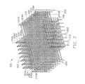
- FIG. 2 is a schematic isometric illustration of a cross-point array 200 according to another embodiment.
- the array 200 as illustrated, has a plurality of bitlines 202 and a plurality of word lines 204 .
- the bitlines 202 and the word lines 204 are arranged perpendicular to one another, but in different planes. In the embodiment shown in FIG. 2 , there are sixty four total bitlines 202 .
- the bitlines 202 are all parallel to one another.
- the bitlines 202 are arranged in eight different horizontal planes with each plane having eight different bitlines 202 .
- the bitlines 202 within a given horizontal plane are all horizontally aligned and parallel.
- bitlines 202 are aligned in eight different vertical planes so that the bitlines 202 within a given vertical plane are all vertically aligned and parallel. It is to be understood that while sixty four bitlines 202 are shown, more or less bitlines 202 may be present.
- each bitline 202 has two ends 206 A, 206 B. Each end 206 A, 206 B of a bitline 202 is coupled to a corresponding conductor 208 , 210 . As shown in FIG. 2 , one conductor 208 extends in a horizontal plane to connect eight bitlines 202 , and the other conductor 210 extends in a vertical plane to connect eight bitlines 202 .
- the vertical conductor 210 connects to a substrate (not shown). To connect the horizontal conductor 208 to the substrate, an additional vertical conductor 212 is utilized. Due to the horizontal conductors 208 and the vertical conductors 210 , an individual bitline 202 may be selected.
- bitline 202 To select an individual bitline 202 , a voltage is provided to horizontal conductor 208 , such as conductor 208 A. By providing voltage to horizontal conductor 208 A, all bitlines 202 connected to conductor 208 A receive a current. Voltage is also provided to a vertical conductor 210 , such as conductor 210 A. By applying voltage to vertical conductor 210 A, all bitlines 202 coupled to conductor 210 A receive current. However, there is only a single bitline 202 A that receives voltage from both conductor 208 A and conductor 210 A. Thus, bitline 202 A is the only bitline selected by delivering current to conductors 208 A and 210 A.
- each bitline 202 includes a first selector switch 214 that is adjacent to one end 206 A of the bitline 202 and a second selector switch 216 that is adjacent to the other end 206 B of the bitline 202 .
- the selector switches 214 , 216 may be ovonic threshold switches.
- the selector switches 214 , 216 may be identical.
- the selector switches 214 , 216 may be different types of selector switches.
- the word lines 204 are all parallel to one another.
- the word lines 204 are arranged in eight different horizontal planes with each plane having eight different word lines 204 .
- the word lines 204 within a given horizontal plane are all horizontally aligned and parallel.
- the word liens 204 are aligned in eight different vertical planes so that the word lines 204 within a given vertical plane are all vertically aligned and parallel. It is to be understood that while sixty four word lines 204 are shown, more or less word lines 204 may be present.
- each word line 204 has two ends 220 A, 220 B. Each end 220 A, 220 B of a word line 204 is coupled to a corresponding conductor 222 , 224 . As shown in FIG. 2 , one conductor 224 extends in a horizontal plane to connect eight word lines 204 , and the other conductor 222 extends in a vertical plane to connect eight word lines 204 .
- the vertical conductor 222 connects to a substrate (not shown). To connect the horizontal conductor 224 to the substrate, an additional vertical conductor 226 is utilized. Due to the horizontal conductors 224 and the vertical conductors 226 , an individual word line 204 may be selected.
- a voltage is provided to horizontal conductor 224 , such as conductor 224 A.
- horizontal conductor 224 A By providing voltage to horizontal conductor 224 A, all word lines 204 connected to conductor 224 A receive a current.
- Voltage is also provided to a vertical conductor 222 , such as conductor 222 A.
- vertical conductor 222 By applying voltage to vertical conductor 222 , all word lines 204 coupled to conductor 222 A receive current.
- word line 204 A is the only word line selected by delivering current to conductors 222 A and 224 A.
- each word line 204 includes a first selector switch 228 that is adjacent to one end 220 A of the word line 204 and a second selector switch 230 that is adjacent to the other end 220 B of the word line 204 .
- the selector switches 228 , 230 may be ovonic threshold switches.
- the selector switches 228 , 230 may be identical.
- the selector switches 228 , 230 may be different types of selector switches.
- selector switches 214 , 216 , 228 , 230 may be identical.
- the selector switches 214 , 216 , 228 , 230 may be different types of selector switches. There is a connection point between each end 220 A, 220 B of the word line 204 and the respective selector switch 228 , 230 . Additionally, there is a connection point between each selector switch 228 , 230 and the corresponding conductor 222 , 224 .
- Selection is accomplished by applying a first voltage to one of the plurality of vertical conductors 210 and a second voltage of reverse polarity to one of the horizontal conductors 208 by means of a vertical conductor 212 from the substrate to the horizontal conductor 208 with a purpose of applying a voltage across the two selector switches 214 , 216 connected to the intended bitline 202 .
- the two selector switches 214 , 216 connecting to a given bitline 202 form a voltage divider thereby keeping the voltage on the bitline 202 near zero.
- Other first and second applied voltages can be used to bias the bitline 202 at a different voltage. As will be discussed below with regards to FIG.
- first and second selector switches 214 , 216 may be fabricated at same end of bitline 202 in close proximity.
- the vertical conductors 210 show that all of the bitline connections in all of the layers can be brought down to logic in the substrate for driving the selection means along the array without the need to expand these vertical conductors 210 in a stairstep-like pattern.
- the vertical conductors 212 show that all of the bitline connections in each of the layers can be brought down from the horizontal conductors 208 to logic in the substrate for driving the selection means with vertical conductors 212 along the near edge of the array 200 without the need to expand these vertical conductors 212 in a stairstep-like pattern.
- selection is accomplished in a similar manner by applying a first voltage to one of the plurality of vertical conductors 222 and a second voltage of reverse polarity to one of the horizontal conductors 224 by means of a vertical conductor 226 from the substrate to the horizontal conductor 224 with a purpose of applying a voltage across the two selector switches 228 , 230 connected to the intended word line 204 .
- the two selector switches 228 , 230 connecting to a given word line 204 form a voltage divider thereby keeping the voltage on the word line 204 near zero.
- Other first and second applied voltages can be used to bias the word line 204 at a different voltage. As will be discussed below with regards to FIG.
- first and second selector switches 228 , 230 may be fabricated at same end of word line 204 in close proximity.
- the vertical conductors 222 show that all of the word line connections in all of the layers can be brought down to logic in the substrate for driving the selection means along the array without the need to expand these vertical conductors 222 in a stairstep-like pattern.
- the vertical conductors 226 show that all of the word line connections in each of the layers can be brought down from the horizontal conductors 224 to logic in the substrate for driving the selection means with vertical conductors 226 along the near edge of the array 200 without the need to expand these vertical conductors 226 in a stairstep-like pattern.
- selector switches 216 , 230 may comprise capacitors such that a bitline and word line are selected simultaneously by capacitive coupling current through selector switches 216 , 230 in order to switch on corresponding selector switches 2214 , 228 respectively.
- the bitline and word line selector switches can be fabricated simultaneously with the selection devices used for individual bits within a memory array. Formation of the selector switches can use a subtractive process where the selector switch material is deposited, followed by photolithographic or other mask patterning, then utilizing an etch such as reaction ion etching to remove all unneeded material and leave pillars of the selector switches.
- OTS materials include but are not limited to the following constituents: Ge, Sb, Te, As, Se, S, Si, In.
- FIG. 3 is a schematic illustration of a memory device 300 coupled to a bitline 302 and a word line 304 .
- Selector switches 306 , 208 are shown on either side of the memory device 300 and coupled to a respective bitline 302 or word line 304 .
- Two selector switches 306 , 308 are shown, but it is to be understood that only a single selector switch needs to be connected to the memory device 300 .
- Two selector switches 306 , 308 are shown simply to illustrate that the selector switch 306 , 308 may be coupled between the memory device 300 and either the bitline 302 or the word line 304 .
- the selector switch 306 , 308 may comprise an OTS device.
- selector switches 214 , 216 , 228 , 230 , 306 , 308 may be identical. In another embodiment, the selector switches 214 , 216 , 228 , 230 , 306 , 308 may be different types of selector switches. It is to be understood that while the memory device 300 is shown as a simple structure, multiple other layers may comprise the memory device 300 such as materials for thermal isolation, chemical barriers layers to prevent mixing and diffusion, and an adhesion layer.
- FIG. 4 is a schematic isometric illustration of bitlines 202 A- 202 H of a cross-point array 400 according to one embodiment.
- the upper array layer 402 connects to a horizontal conductor 406 A through selector switches 408 A, and the lower array layer 404 connected to a horizontal conductor 406 B through selector switches 408 B.
- Bitlines 202 A, 202 E are connected to vertical conductor 410 through selector switches 412 A, 412 B.
- Bitlines 202 B, 202 F are connected to vertical conductor 414 through selector switches.
- Bitlines 202 C, 202 G are connected to vertical conductor 416 through selector switches.
- Bitlines 202 D, 202 H are connected to vertical conductor 418 through selector switches.
- the connections from the bitlines 202 A- 202 H to the respective conductors 406 A, 406 B, 410 , 414 , 416 , 418 is made at the same end of the bitlines 202 A- 202 H.
- FIG. 5 is a schematic isometric illustration of word lines 204 A- 204 H of a cross-point array 500 according to one embodiment.
- the upper array layer 502 connects to a horizontal conductor 506 A through selector switches 508 A, and the lower array layer 504 connected to a horizontal conductor 506 B through selector switches 508 A.
- Word lines 204 A, 204 E are connected to vertical conductor 510 through selector switches 512 A, 512 B.
- Word lines 204 B, 204 F are connected to vertical conductor 514 through selector switches.
- Word lines 204 C, 204 G are connected to vertical conductor 516 through selector switches.
- Word lines 204 D, 204 H are connected to vertical conductor 518 through selector switches.
- the connections from the word lines 204 A- 204 H to the respective conductors 506 A, 506 B, 510 , 514 , 516 , 518 is made at the same end of the word lines 204 A- 204 H.
- FIG. 6 is a schematic isometric illustration of bitlines and word lines of a cross-point array 600 according to one embodiment.
- the horizontal conductors 406 A, 406 B are shown to wrap around the vertical conductors 410 , 414 , 416 , 418 so that the horizontal conductors 406 A, 406 B connect to the substrate on the same side as the vertical conductors 410 , 414 , 416 , 418 for the bitlines 202 A, 202 E.
- first elements 610 A, 610 B, respective second elements 612 A, 612 B and respective third elements 614 A, 614 B are all disposed in within the same plane for a given horizontal conductor 406 A, 406 B.
- First elements 610 A, 610 B extend substantially perpendicular to the horizontal conductors 406 A, 406 B.
- Second elements 612 A, 612 B extend substantially perpendicular to the first elements 610 A, 610 B and parallel to the horizontal conductors 406 A, 406 B.
- the third elements 614 A, 614 B are parallel to the vertical conductors 410 , 414 , 416 , 418 . It is to be noted that the first elements 610 A, 610 B are vertically aligned in a first vertical plane, the second elements 612 A, 612 B are vertically aligned in a second vertical plane, and the third elements 614 A, 614 B are aligned within a plane that is perpendicular to the first and second vertical planes. As such, the first elements 610 A, 610 B, second elements 612 A, 612 B and third elements 614 A, 614 B collectively wrap around the vertical conductors 410 , 414 , 416 , 418 .
- selector switches along the same bitline have different areas/volumes.
- selector switch 412 A coupled between the bitline 202 A and the vertical conductor 410 has a greater area/volume than the selector switch 408 A coupled between the horizontal conductor 406 A and the bitline 202 A.
- the selector switches 408 A, 408 B between the horizontal conductors 406 A, 406 B and the bitlines 202 A- 202 H have a smaller area/volume than the selector switches 412 A, 412 B between the vertical conductors 410 , 414 , 416 , 418 and the bitlines 202 A- 202 H.
- selector switches 412 A, 412 B between the vertical conductors 410 , 414 , 416 , 418 and the bitlines 202 A- 202 H may have a smaller area/volume than the selector switches 408 A, 408 B between the horizontal conductors 406 A, 406 B and the bitlines 202 A- 202 H.
- selector switches 412 A, 412 B may not be identical and that the selector switches 408 A, 408 B may not be identical such that the smaller selector switch area/volume may be connected to the vertical connector 410 , 414 , 416 , 418 for one bitline 202 A- 202 H while the smaller selector switch area/volume may be connected to the horizontal conductor 406 A, 406 B for another bitline.
- the benefit of having different area/volumes for the switching elements is that when equal current is passed through both selector switches for a given bitline, greater voltage occurs across the selector switch having the smaller area/volume.
- the respective word lines and bitlines may be actively driving a memory cell above or below it so that the voltages will be reversed depositing upon whether going up or down.
- the selectors are voltage thresholds driven regardless of polarity so bitlines and word lines can be selected in either polarity.
- FIG. 7 is a schematic isometric illustration of word lines and bitlines of a cross-point array 700 according to one embodiment.
- the horizontal conductors 506 A, 506 B are shown to wrap around the vertical conductors 510 , 514 , 516 , 518 so that the horizontal conductors 506 A, 506 B connect to the substrate on the same side as the vertical conductors 510 , 514 , 516 , 518 for the word lines 204 A, 204 E.
- first elements 710 A, 710 B respective second elements 712 A, 712 B and respective third elements 714 A, 714 B.
- Respective first elements 710 A, 710 B, second elements 712 A, 712 B and the horizontal conductors 506 A, 506 B are all disposed in within the same plane for a given horizontal conductor 506 A, 506 B.
- First elements 710 A, 710 B extend substantially perpendicular to the horizontal conductors 506 A, 506 B.
- Second elements 712 A, 712 B extend substantially perpendicular to the first elements 710 A, 710 B and parallel to the horizontal conductors 506 A, 506 B.
- the third elements 714 A, 714 B are parallel to the vertical conductors 510 , 514 , 516 , 518 . It is to be noted that the first elements 710 A, 710 B are vertically aligned in a first vertical plane, the second elements 712 A, 712 B are vertically aligned in a second vertical plane, and the third elements 714 A, 714 B are aligned within a plane that is perpendicular to the first and second vertical planes. As such, the first elements 710 A, 710 B, second elements 712 A, 712 B and third elements 714 A, 714 B collectively wrap around the vertical conductors 510 , 514 , 516 , 518 .
- selector switches along the same word lines have different areas/volumes.
- selector switch 512 A coupled between the word line 204 A and the vertical conductor 510 has a greater area/volume than the selector switch 508 A coupled between the horizontal conductor 506 A and the word line 204 A.
- the selector switches 508 A, 508 B between the horizontal conductors 506 A, 506 B and the word lines 204 A- 204 H have a smaller area/volume than the selector switches 512 A, 512 B between the vertical conductors 510 , 514 , 516 , 518 and the word lines 204 A- 204 H.
- selector switches 512 A, 512 B between the vertical conductors 510 , 514 , 516 , 518 and the word lines 204 A- 204 H may have a smaller area/volume than the selector switches 508 A, 508 B between the horizontal conductors 506 A, 506 B and the word lines 204 A- 204 H.
- selector switches 512 A, 512 B may not be identical and that the selector switches 508 A, 508 B may not be identical such that the smaller selector switch area/volume may be connected to the vertical connector 510 , 514 , 516 , 518 for one word line 204 A- 204 H while the smaller selector switch area/volume may be connected to the horizontal conductor 506 A, 506 B for another bitline.
- the benefit of having different area/volumes for the switching elements is that when equal current is passed through both selector switches for a given bitline, greater voltage occurs across the selector switch having the smaller area/volume.
- the glitch control can be controlled by leveraging the capacitance of the bitline (or word line) in a densely packed plurality of bitlines (or word lines) to filter the glitch.
- the threshold of the memory cells could be designed to be above that which might occur due to a glitch.
- the voltage divider formed by the two selector switches can be adjusted by designing the two selector switches to be manufactured in parallel (such that the threshold voltages of the two selector switches is the same due to the matched thickness of the selector switch material) while also designing the two selector switches to have different areas such that a given current flowing in series through the two selector switches will result in a different voltage on each selector switch (i.e., the area determines the relative resistances of the respective selector switches which, following Ohms's Law, will result in a different voltage across each of the two selector switches and an adjusted voltage for the voltage divider formed by these two selector switches).
- the different voltage on each selector switch will result in one selector switch having a higher voltage across it than the other and will thereby allow for a design that can control which selector switch will switch first and what polarity any voltage glitch will assume.
- a small holding current is maintained to keep the selector switches in their low resistance, switched state.
- the bias voltage for providing the holding current can be adjusted to keep the voltage on the selected bitline (or word line) at a desired voltage level. Note that the area would be changed by increasing the dimension running in parallel with the direction of the bitline (not in the direction orthogonal to the bitline) because the orthogonal direction feature size is constrained to fit within the array pitch.
- a 3D cross-point memory array may be fabricated to utilize less substrate area and thus be less complex due to the horizontal and vertical bitline and word line connectors.
- the selecting switch permits the array to operate efficiently.
- the array is easy to operate by selecting a bitline and word line to select a particular memory device. Following the selection of a bitline and a word line as described above, the bias voltage of the bitline and the bias voltage of the word line can be used to manipulate the voltage across the memory cell at the intersection of the selected bitline and the selected word line to measure (i.e., read) and alter (i.e., write and/or erase) the state of that memory cell.
Landscapes
- Semiconductor Memories (AREA)
Abstract
Description
Claims (29)
Priority Applications (1)
| Application Number | Priority Date | Filing Date | Title |
|---|---|---|---|
| US15/098,963 US9837471B2 (en) | 2016-04-14 | 2016-04-14 | Dual OTS memory cell selection means and method |
Applications Claiming Priority (1)
| Application Number | Priority Date | Filing Date | Title |
|---|---|---|---|
| US15/098,963 US9837471B2 (en) | 2016-04-14 | 2016-04-14 | Dual OTS memory cell selection means and method |
Publications (2)
| Publication Number | Publication Date |
|---|---|
| US20170301732A1 US20170301732A1 (en) | 2017-10-19 |
| US9837471B2 true US9837471B2 (en) | 2017-12-05 |
Family
ID=60039026
Family Applications (1)
| Application Number | Title | Priority Date | Filing Date |
|---|---|---|---|
| US15/098,963 Active US9837471B2 (en) | 2016-04-14 | 2016-04-14 | Dual OTS memory cell selection means and method |
Country Status (1)
| Country | Link |
|---|---|
| US (1) | US9837471B2 (en) |
Cited By (5)
| Publication number | Priority date | Publication date | Assignee | Title |
|---|---|---|---|---|
| US10559752B2 (en) * | 2016-12-05 | 2020-02-11 | Samsung Electronics Co., Ltd. | Semiconductor device and method for fabricating the same |
| US10825862B2 (en) | 2018-10-05 | 2020-11-03 | Samsung Electronics Co., Ltd. | Variable resistance memory device |
| US10937833B2 (en) | 2018-06-29 | 2021-03-02 | Samsung Electronics Co., Ltd. | Variable resistance memory device |
| US11211427B2 (en) | 2018-09-13 | 2021-12-28 | Samsung Electronics Co., Ltd. | Switching element, variable resistance memory device, and method of manufacturing the switching element |
| WO2022077147A1 (en) * | 2020-10-12 | 2022-04-21 | Yangtze Advanced Memory Industrial Innovation Center Co., Ltd | Novel integration scheme with cpu bonding to 3d xpoint chip |
Families Citing this family (1)
| Publication number | Priority date | Publication date | Assignee | Title |
|---|---|---|---|---|
| US11049555B1 (en) * | 2020-05-08 | 2021-06-29 | Taiwan Semiconductor Manufacturing Company, Ltd. | SRAM power-up random number generator |
Citations (12)
| Publication number | Priority date | Publication date | Assignee | Title |
|---|---|---|---|---|
| US20090244796A1 (en) * | 2008-03-31 | 2009-10-01 | Tang Stephen H | Electrostatic discharge protection circuit including ovonic threshold switches |
| US20090310402A1 (en) * | 2008-06-17 | 2009-12-17 | Ovonyx, Inc. | Method and apparatus for decoding memory |
| US20100232200A1 (en) * | 2009-03-10 | 2010-09-16 | Shepard Daniel R | Vertical switch three-dimensional memory array |
| US8488374B2 (en) | 2010-06-07 | 2013-07-16 | Micron Technology, Inc. | Memory arrays |
| US20130194855A1 (en) * | 2012-01-26 | 2013-08-01 | Luiz M. Franca-Neto | High current capable access device for three-dimensional solid-state memory |
| US20140063888A1 (en) * | 2012-08-29 | 2014-03-06 | Micron Technology, Inc. | Memory array plane select and methods |
| US8766234B1 (en) | 2012-12-27 | 2014-07-01 | Intermolecular, Inc. | Current selector for non-volatile memory in a cross bar array based on defect and band engineering metal-dielectric-metal stacks |
| US8923032B2 (en) | 2011-12-07 | 2014-12-30 | Panasonic Corporation | Crosspoint nonvolatile memory device and forming method thereof |
| US20150044849A1 (en) | 2012-08-31 | 2015-02-12 | Micron Technology, Inc. | Three dimensional memory array architecture |
| US9118004B2 (en) | 2011-03-23 | 2015-08-25 | Micron Technology, Inc. | Memory cells and methods of forming memory cells |
| US9147439B2 (en) | 2012-06-15 | 2015-09-29 | Sandisk 3D Llc | Non-volatile memory having 3D array architecture with staircase word lines and vertical bit lines and methods thereof |
| US9172037B2 (en) | 2012-02-02 | 2015-10-27 | Micron Technology, Inc. | Combined conductive plug/conductive line memory arrays and methods of forming the same |
-
2016
- 2016-04-14 US US15/098,963 patent/US9837471B2/en active Active
Patent Citations (13)
| Publication number | Priority date | Publication date | Assignee | Title |
|---|---|---|---|---|
| US20090244796A1 (en) * | 2008-03-31 | 2009-10-01 | Tang Stephen H | Electrostatic discharge protection circuit including ovonic threshold switches |
| US20090310402A1 (en) * | 2008-06-17 | 2009-12-17 | Ovonyx, Inc. | Method and apparatus for decoding memory |
| US20100232200A1 (en) * | 2009-03-10 | 2010-09-16 | Shepard Daniel R | Vertical switch three-dimensional memory array |
| US8488374B2 (en) | 2010-06-07 | 2013-07-16 | Micron Technology, Inc. | Memory arrays |
| US9118004B2 (en) | 2011-03-23 | 2015-08-25 | Micron Technology, Inc. | Memory cells and methods of forming memory cells |
| US8923032B2 (en) | 2011-12-07 | 2014-12-30 | Panasonic Corporation | Crosspoint nonvolatile memory device and forming method thereof |
| US20130194855A1 (en) * | 2012-01-26 | 2013-08-01 | Luiz M. Franca-Neto | High current capable access device for three-dimensional solid-state memory |
| US20140204646A1 (en) * | 2012-01-26 | 2014-07-24 | HGST Netherlands B.V. | High current capable access device for three-dimensional solid-state memory |
| US9172037B2 (en) | 2012-02-02 | 2015-10-27 | Micron Technology, Inc. | Combined conductive plug/conductive line memory arrays and methods of forming the same |
| US9147439B2 (en) | 2012-06-15 | 2015-09-29 | Sandisk 3D Llc | Non-volatile memory having 3D array architecture with staircase word lines and vertical bit lines and methods thereof |
| US20140063888A1 (en) * | 2012-08-29 | 2014-03-06 | Micron Technology, Inc. | Memory array plane select and methods |
| US20150044849A1 (en) | 2012-08-31 | 2015-02-12 | Micron Technology, Inc. | Three dimensional memory array architecture |
| US8766234B1 (en) | 2012-12-27 | 2014-07-01 | Intermolecular, Inc. | Current selector for non-volatile memory in a cross bar array based on defect and band engineering metal-dielectric-metal stacks |
Non-Patent Citations (1)
| Title |
|---|
| Jo, et al.; 3D-stackable Crossbar Resistive Memory based on Field Assisted Superlinear Threshold (FAST) Selector; dated 2014; 4 total pages. |
Cited By (6)
| Publication number | Priority date | Publication date | Assignee | Title |
|---|---|---|---|---|
| US10559752B2 (en) * | 2016-12-05 | 2020-02-11 | Samsung Electronics Co., Ltd. | Semiconductor device and method for fabricating the same |
| US10937833B2 (en) | 2018-06-29 | 2021-03-02 | Samsung Electronics Co., Ltd. | Variable resistance memory device |
| US11538861B2 (en) | 2018-06-29 | 2022-12-27 | Samsung Electronics Co., Ltd. | Variable resistance memory device |
| US11211427B2 (en) | 2018-09-13 | 2021-12-28 | Samsung Electronics Co., Ltd. | Switching element, variable resistance memory device, and method of manufacturing the switching element |
| US10825862B2 (en) | 2018-10-05 | 2020-11-03 | Samsung Electronics Co., Ltd. | Variable resistance memory device |
| WO2022077147A1 (en) * | 2020-10-12 | 2022-04-21 | Yangtze Advanced Memory Industrial Innovation Center Co., Ltd | Novel integration scheme with cpu bonding to 3d xpoint chip |
Also Published As
| Publication number | Publication date |
|---|---|
| US20170301732A1 (en) | 2017-10-19 |
Similar Documents
| Publication | Publication Date | Title |
|---|---|---|
| US9837471B2 (en) | Dual OTS memory cell selection means and method | |
| US10510773B2 (en) | Apparatuses having a ferroelectric field-effect transistor memory array and related method | |
| JP5722874B2 (en) | Three-dimensional array of reprogrammable non-volatile memory elements having vertical bit line and single sided word line architectures | |
| KR101726460B1 (en) | Three-dimensional array of re-programmable non-volatile memory elements having vertical bit lines | |
| US7742331B2 (en) | Nonvolatile semiconductor memory device and data erase/write method thereof | |
| US7986545B2 (en) | Non-volatile memory device and method of operating the same | |
| KR101728934B1 (en) | Non-volatile memory having 3d array of read/write elements with low current structures and methods thereof | |
| EP2580756B1 (en) | Non-volatile memory having 3d array of read/write elements and read/write circuits and method thereof | |
| US7633789B2 (en) | Planar third dimensional memory with multi-port access | |
| US9064547B2 (en) | 3D non-volatile memory having low-current cells and methods | |
| KR102735066B1 (en) | Three Dimensional Resistive Memory Device | |
| RU2642960C2 (en) | Semiconductor memory device | |
| US8687406B2 (en) | Semiconductor memory device and method of controlling the same | |
| WO2004084229A1 (en) | Programmable resistance memory device | |
| TW201214441A (en) | Single device driver circuit to control three-dimensional memory element array | |
| US20170316824A1 (en) | Multi-layer resistive memory devices | |
| US9245621B2 (en) | Semiconductor memory device executing a write operation with first and second voltage applications | |
| US20090020785A1 (en) | Semiconductor integrated circuit device | |
| US9953705B2 (en) | Planar memory cell architectures in resistive memory devices | |
| US11100988B2 (en) | Semiconductor memory device | |
| CN114639773A (en) | Semiconductor structure, memory unit and memory array | |
| CN113078182B (en) | Three-dimensional resistive memory device | |
| US9941331B1 (en) | Device with sub-minimum pitch and method of making | |
| WO2024174309A1 (en) | Fuse array circuit and memory | |
| KR20230001275A (en) | Variable resistance memory device including a plurality of stacked memory cells |
Legal Events
| Date | Code | Title | Description |
|---|---|---|---|
| AS | Assignment |
Owner name: HGST NETHERLANDS B.V., NETHERLANDS Free format text: ASSIGNMENT OF ASSIGNORS INTEREST;ASSIGNORS:SHEPARD, DANIEL ROBERT;APODACA, MAC D.;SIGNING DATES FROM 20160411 TO 20160412;REEL/FRAME:038291/0357 |
|
| AS | Assignment |
Owner name: WESTERN DIGITAL TECHNOLOGIES, INC., CALIFORNIA Free format text: ASSIGNMENT OF ASSIGNORS INTEREST;ASSIGNOR:HGST NETHERLANDS B.V.;REEL/FRAME:040831/0265 Effective date: 20160831 |
|
| AS | Assignment |
Owner name: WESTERN DIGITAL TECHNOLOGIES, INC., CALIFORNIA Free format text: CORRECTIVE ASSIGNMENT TO CORRECT THE INCORRECT SERIAL NO 15/025,946 PREVIOUSLY RECORDED AT REEL: 040831 FRAME: 0265. ASSIGNOR(S) HEREBY CONFIRMS THE ASSIGNMENT;ASSIGNOR:HGST NETHERLANDS B.V.;REEL/FRAME:043973/0762 Effective date: 20160831 |
|
| STCF | Information on status: patent grant |
Free format text: PATENTED CASE |
|
| AS | Assignment |
Owner name: JPMORGAN CHASE BANK, N.A., AS AGENT, ILLINOIS Free format text: SECURITY INTEREST;ASSIGNOR:WESTERN DIGITAL TECHNOLOGIES, INC.;REEL/FRAME:052915/0566 Effective date: 20200113 |
|
| MAFP | Maintenance fee payment |
Free format text: PAYMENT OF MAINTENANCE FEE, 4TH YEAR, LARGE ENTITY (ORIGINAL EVENT CODE: M1551); ENTITY STATUS OF PATENT OWNER: LARGE ENTITY Year of fee payment: 4 |
|
| AS | Assignment |
Owner name: WESTERN DIGITAL TECHNOLOGIES, INC., CALIFORNIA Free format text: RELEASE OF SECURITY INTEREST AT REEL 052915 FRAME 0566;ASSIGNOR:JPMORGAN CHASE BANK, N.A.;REEL/FRAME:059127/0001 Effective date: 20220203 |
|
| AS | Assignment |
Owner name: JPMORGAN CHASE BANK, N.A., ILLINOIS Free format text: PATENT COLLATERAL AGREEMENT - A&R LOAN AGREEMENT;ASSIGNOR:WESTERN DIGITAL TECHNOLOGIES, INC.;REEL/FRAME:064715/0001 Effective date: 20230818 Owner name: JPMORGAN CHASE BANK, N.A., ILLINOIS Free format text: PATENT COLLATERAL AGREEMENT - DDTL LOAN AGREEMENT;ASSIGNOR:WESTERN DIGITAL TECHNOLOGIES, INC.;REEL/FRAME:067045/0156 Effective date: 20230818 |
|
| AS | Assignment |
Owner name: SANDISK TECHNOLOGIES, INC., CALIFORNIA Free format text: ASSIGNMENT OF ASSIGNORS INTEREST;ASSIGNOR:WESTERN DIGITAL TECHNOLOGIES, INC.;REEL/FRAME:067567/0682 Effective date: 20240503 |
|
| AS | Assignment |
Owner name: SANDISK TECHNOLOGIES, INC., CALIFORNIA Free format text: CHANGE OF NAME;ASSIGNOR:SANDISK TECHNOLOGIES, INC.;REEL/FRAME:067982/0032 Effective date: 20240621 |
|
| AS | Assignment |
Owner name: JPMORGAN CHASE BANK, N.A., AS THE AGENT, ILLINOIS Free format text: PATENT COLLATERAL AGREEMENT;ASSIGNOR:SANDISK TECHNOLOGIES, INC.;REEL/FRAME:068762/0494 Effective date: 20240820 |
|
| AS | Assignment |
Owner name: SAMSUNG ELECTRONICS CO., LTD., KOREA, REPUBLIC OF Free format text: ASSIGNMENT OF ASSIGNORS INTEREST;ASSIGNOR:SANDISK TECHNOLOGIES, INC.;REEL/FRAME:070778/0160 Effective date: 20250306 |
|
| MAFP | Maintenance fee payment |
Free format text: PAYMENT OF MAINTENANCE FEE, 8TH YEAR, LARGE ENTITY (ORIGINAL EVENT CODE: M1552); ENTITY STATUS OF PATENT OWNER: LARGE ENTITY Year of fee payment: 8 |