US9836232B1 - Data storage device and method for using secondary non-volatile memory for temporary metadata storage - Google Patents
Data storage device and method for using secondary non-volatile memory for temporary metadata storage Download PDFInfo
- Publication number
- US9836232B1 US9836232B1 US14/870,571 US201514870571A US9836232B1 US 9836232 B1 US9836232 B1 US 9836232B1 US 201514870571 A US201514870571 A US 201514870571A US 9836232 B1 US9836232 B1 US 9836232B1
- Authority
- US
- United States
- Prior art keywords
- metadata
- nvm
- volatile memory
- storage device
- primary
- Prior art date
- Legal status (The legal status is an assumption and is not a legal conclusion. Google has not performed a legal analysis and makes no representation as to the accuracy of the status listed.)
- Active, expires
Links
Images


Classifications
-
- G—PHYSICS
- G06—COMPUTING; CALCULATING OR COUNTING
- G06F—ELECTRIC DIGITAL DATA PROCESSING
- G06F3/00—Input arrangements for transferring data to be processed into a form capable of being handled by the computer; Output arrangements for transferring data from processing unit to output unit, e.g. interface arrangements
- G06F3/06—Digital input from, or digital output to, record carriers, e.g. RAID, emulated record carriers or networked record carriers
- G06F3/0601—Interfaces specially adapted for storage systems
- G06F3/0628—Interfaces specially adapted for storage systems making use of a particular technique
- G06F3/0655—Vertical data movement, i.e. input-output transfer; data movement between one or more hosts and one or more storage devices
- G06F3/0656—Data buffering arrangements
-
- G—PHYSICS
- G06—COMPUTING; CALCULATING OR COUNTING
- G06F—ELECTRIC DIGITAL DATA PROCESSING
- G06F3/00—Input arrangements for transferring data to be processed into a form capable of being handled by the computer; Output arrangements for transferring data from processing unit to output unit, e.g. interface arrangements
- G06F3/06—Digital input from, or digital output to, record carriers, e.g. RAID, emulated record carriers or networked record carriers
- G06F3/0601—Interfaces specially adapted for storage systems
- G06F3/0602—Interfaces specially adapted for storage systems specifically adapted to achieve a particular effect
- G06F3/0614—Improving the reliability of storage systems
- G06F3/0619—Improving the reliability of storage systems in relation to data integrity, e.g. data losses, bit errors
-
- G—PHYSICS
- G06—COMPUTING; CALCULATING OR COUNTING
- G06F—ELECTRIC DIGITAL DATA PROCESSING
- G06F11/00—Error detection; Error correction; Monitoring
- G06F11/07—Responding to the occurrence of a fault, e.g. fault tolerance
- G06F11/14—Error detection or correction of the data by redundancy in operation
- G06F11/1402—Saving, restoring, recovering or retrying
- G06F11/1415—Saving, restoring, recovering or retrying at system level
- G06F11/1441—Resetting or repowering
-
- G—PHYSICS
- G06—COMPUTING; CALCULATING OR COUNTING
- G06F—ELECTRIC DIGITAL DATA PROCESSING
- G06F12/00—Accessing, addressing or allocating within memory systems or architectures
- G06F12/02—Addressing or allocation; Relocation
- G06F12/08—Addressing or allocation; Relocation in hierarchically structured memory systems, e.g. virtual memory systems
- G06F12/0802—Addressing of a memory level in which the access to the desired data or data block requires associative addressing means, e.g. caches
- G06F12/0804—Addressing of a memory level in which the access to the desired data or data block requires associative addressing means, e.g. caches with main memory updating
-
- G—PHYSICS
- G06—COMPUTING; CALCULATING OR COUNTING
- G06F—ELECTRIC DIGITAL DATA PROCESSING
- G06F12/00—Accessing, addressing or allocating within memory systems or architectures
- G06F12/02—Addressing or allocation; Relocation
- G06F12/08—Addressing or allocation; Relocation in hierarchically structured memory systems, e.g. virtual memory systems
- G06F12/0802—Addressing of a memory level in which the access to the desired data or data block requires associative addressing means, e.g. caches
- G06F12/0866—Addressing of a memory level in which the access to the desired data or data block requires associative addressing means, e.g. caches for peripheral storage systems, e.g. disk cache
- G06F12/0868—Data transfer between cache memory and other subsystems, e.g. storage devices or host systems
-
- G—PHYSICS
- G06—COMPUTING; CALCULATING OR COUNTING
- G06F—ELECTRIC DIGITAL DATA PROCESSING
- G06F3/00—Input arrangements for transferring data to be processed into a form capable of being handled by the computer; Output arrangements for transferring data from processing unit to output unit, e.g. interface arrangements
- G06F3/06—Digital input from, or digital output to, record carriers, e.g. RAID, emulated record carriers or networked record carriers
- G06F3/0601—Interfaces specially adapted for storage systems
- G06F3/0602—Interfaces specially adapted for storage systems specifically adapted to achieve a particular effect
- G06F3/061—Improving I/O performance
- G06F3/0613—Improving I/O performance in relation to throughput
-
- G—PHYSICS
- G06—COMPUTING; CALCULATING OR COUNTING
- G06F—ELECTRIC DIGITAL DATA PROCESSING
- G06F3/00—Input arrangements for transferring data to be processed into a form capable of being handled by the computer; Output arrangements for transferring data from processing unit to output unit, e.g. interface arrangements
- G06F3/06—Digital input from, or digital output to, record carriers, e.g. RAID, emulated record carriers or networked record carriers
- G06F3/0601—Interfaces specially adapted for storage systems
- G06F3/0628—Interfaces specially adapted for storage systems making use of a particular technique
- G06F3/0638—Organizing or formatting or addressing of data
- G06F3/0644—Management of space entities, e.g. partitions, extents, pools
-
- G—PHYSICS
- G06—COMPUTING; CALCULATING OR COUNTING
- G06F—ELECTRIC DIGITAL DATA PROCESSING
- G06F3/00—Input arrangements for transferring data to be processed into a form capable of being handled by the computer; Output arrangements for transferring data from processing unit to output unit, e.g. interface arrangements
- G06F3/06—Digital input from, or digital output to, record carriers, e.g. RAID, emulated record carriers or networked record carriers
- G06F3/0601—Interfaces specially adapted for storage systems
- G06F3/0628—Interfaces specially adapted for storage systems making use of a particular technique
- G06F3/0646—Horizontal data movement in storage systems, i.e. moving data in between storage devices or systems
- G06F3/0647—Migration mechanisms
-
- G—PHYSICS
- G06—COMPUTING; CALCULATING OR COUNTING
- G06F—ELECTRIC DIGITAL DATA PROCESSING
- G06F3/00—Input arrangements for transferring data to be processed into a form capable of being handled by the computer; Output arrangements for transferring data from processing unit to output unit, e.g. interface arrangements
- G06F3/06—Digital input from, or digital output to, record carriers, e.g. RAID, emulated record carriers or networked record carriers
- G06F3/0601—Interfaces specially adapted for storage systems
- G06F3/0668—Interfaces specially adapted for storage systems adopting a particular infrastructure
- G06F3/0671—In-line storage system
- G06F3/0673—Single storage device
- G06F3/068—Hybrid storage device
-
- G—PHYSICS
- G06—COMPUTING; CALCULATING OR COUNTING
- G06F—ELECTRIC DIGITAL DATA PROCESSING
- G06F3/00—Input arrangements for transferring data to be processed into a form capable of being handled by the computer; Output arrangements for transferring data from processing unit to output unit, e.g. interface arrangements
- G06F3/06—Digital input from, or digital output to, record carriers, e.g. RAID, emulated record carriers or networked record carriers
- G06F3/0601—Interfaces specially adapted for storage systems
- G06F3/0668—Interfaces specially adapted for storage systems adopting a particular infrastructure
- G06F3/0671—In-line storage system
- G06F3/0683—Plurality of storage devices
- G06F3/0685—Hybrid storage combining heterogeneous device types, e.g. hierarchical storage, hybrid arrays
-
- G—PHYSICS
- G06—COMPUTING; CALCULATING OR COUNTING
- G06F—ELECTRIC DIGITAL DATA PROCESSING
- G06F3/00—Input arrangements for transferring data to be processed into a form capable of being handled by the computer; Output arrangements for transferring data from processing unit to output unit, e.g. interface arrangements
- G06F3/06—Digital input from, or digital output to, record carriers, e.g. RAID, emulated record carriers or networked record carriers
- G06F3/0601—Interfaces specially adapted for storage systems
- G06F3/0668—Interfaces specially adapted for storage systems adopting a particular infrastructure
- G06F3/0671—In-line storage system
- G06F3/0683—Plurality of storage devices
- G06F3/0688—Non-volatile semiconductor memory arrays
-
- G—PHYSICS
- G06—COMPUTING; CALCULATING OR COUNTING
- G06F—ELECTRIC DIGITAL DATA PROCESSING
- G06F12/00—Accessing, addressing or allocating within memory systems or architectures
- G06F12/02—Addressing or allocation; Relocation
- G06F12/08—Addressing or allocation; Relocation in hierarchically structured memory systems, e.g. virtual memory systems
- G06F12/0802—Addressing of a memory level in which the access to the desired data or data block requires associative addressing means, e.g. caches
- G06F12/0893—Caches characterised by their organisation or structure
- G06F12/0897—Caches characterised by their organisation or structure with two or more cache hierarchy levels
-
- G—PHYSICS
- G06—COMPUTING; CALCULATING OR COUNTING
- G06F—ELECTRIC DIGITAL DATA PROCESSING
- G06F2212/00—Indexing scheme relating to accessing, addressing or allocation within memory systems or architectures
- G06F2212/10—Providing a specific technical effect
- G06F2212/1016—Performance improvement
-
- G—PHYSICS
- G06—COMPUTING; CALCULATING OR COUNTING
- G06F—ELECTRIC DIGITAL DATA PROCESSING
- G06F2212/00—Indexing scheme relating to accessing, addressing or allocation within memory systems or architectures
- G06F2212/10—Providing a specific technical effect
- G06F2212/1032—Reliability improvement, data loss prevention, degraded operation etc
-
- G—PHYSICS
- G06—COMPUTING; CALCULATING OR COUNTING
- G06F—ELECTRIC DIGITAL DATA PROCESSING
- G06F2212/00—Indexing scheme relating to accessing, addressing or allocation within memory systems or architectures
- G06F2212/22—Employing cache memory using specific memory technology
- G06F2212/225—Hybrid cache memory, e.g. having both volatile and non-volatile portions
-
- G—PHYSICS
- G06—COMPUTING; CALCULATING OR COUNTING
- G06F—ELECTRIC DIGITAL DATA PROCESSING
- G06F2212/00—Indexing scheme relating to accessing, addressing or allocation within memory systems or architectures
- G06F2212/46—Caching storage objects of specific type in disk cache
- G06F2212/461—Sector or disk block
-
- G—PHYSICS
- G06—COMPUTING; CALCULATING OR COUNTING
- G06F—ELECTRIC DIGITAL DATA PROCESSING
- G06F2212/00—Indexing scheme relating to accessing, addressing or allocation within memory systems or architectures
- G06F2212/46—Caching storage objects of specific type in disk cache
- G06F2212/466—Metadata, control data
-
- G—PHYSICS
- G06—COMPUTING; CALCULATING OR COUNTING
- G06F—ELECTRIC DIGITAL DATA PROCESSING
- G06F2212/00—Indexing scheme relating to accessing, addressing or allocation within memory systems or architectures
- G06F2212/72—Details relating to flash memory management
- G06F2212/7201—Logical to physical mapping or translation of blocks or pages
Definitions
- Data storage devices such as hard disk drives (HDDs), solid-state hybrid drives (SSHDs), or solid-state drives (SSDs)
- HDDs hard disk drives
- SSHDs solid-state hybrid drives
- SSDs solid-state drives
- NVM non-volatile memory
- the primary data storage location is generally provided by rotating magnetic media (one or more disks)
- non-volatile solid-state memory e.g., NAND
- the temporary storage location is typically provided by DRAM.
- DRAM volatile memory
- the primary storage location e.g., a disk
- the host data is safe from loss resulting from an interruption (either intentional or unexpected) in power supplied to the data storage device.
- the host data resides in the temporary storage location (e.g., DRAM), it is susceptible to loss from an interruption in supplied power.
- FIG. 1A is a block diagram showing a data storage device including control circuitry in communication with a primary non-volatile memory (NVM), a boot code NVM, a secondary NVM for temporarily storing metadata, and volatile memory, in accordance with one embodiment of the invention.
- NVM non-volatile memory
- boot code NVM boot code NVM
- secondary NVM secondary NVM for temporarily storing metadata
- volatile memory volatile memory
- FIG. 1B is a flow diagram showing a process in which a first condition determines when metadata associated with one or more host write commands that is accumulated in volatile memory is written to a secondary NVM, and in which a second condition determines when at least a portion of the metadata accumulated in the secondary NVM or the volatile memory is written to a primary NVM, in accordance with one embodiment of the invention.
- FIG. 2A is a block diagram showing a data storage device including control circuitry in communication with a primary NVM, a secondary NVM including a shared region and a metadata region, and volatile memory, in accordance with one embodiment of the invention.
- FIG. 2B is a flow diagram showing a process in which a first condition determines when metadata associated with one or more host write commands that is accumulated in volatile memory is written to a metadata region of a secondary NVM, and in which a second condition determines when at least a portion of the metadata accumulated in the secondary NVM metadata region or the volatile memory is written to a primary NVM, in accordance with one embodiment of the invention.
- FIG. 3A is a block diagram showing a data storage device including control circuitry in communication with a primary NVM, a first and a second secondary NVM for temporarily storing metadata, and volatile memory, in accordance with one embodiment of the invention.
- FIG. 3B is a flow diagram showing a process in which a first condition determines when metadata associated with one or more host write commands that is accumulated in volatile memory is written to a first or a second secondary NVM, and in which a second condition determines when at least a portion of the metadata accumulated in the first or the second secondary NVM or the volatile memory is written to a primary NVM, in accordance with one embodiment of the invention.
- FIG. 4A is a block diagram showing a data storage device including control circuitry in communication with a primary NVM including a disk, a secondary NVM for temporarily storing metadata, and a volatile memory, in accordance with one embodiment of the invention.
- FIG. 4B is a flow diagram showing a process in which a first condition determines when metadata associated with one or more host write commands that is accumulated in volatile memory is written to a secondary NVM, and in which a second condition determines when at least a portion of the metadata accumulated in the secondary NVM or the volatile memory is written to a primary NVM, in accordance with one embodiment of the invention.
- FIG. 4C is a diagram showing an example of a zone including shingled data tracks in the disk shown in FIG. 4B .
- FIG. 5 is a block diagram showing an example of a primary NVM including a disk including a mainstore and a media-based cache (MBC) for storing user data and a metadata storage region.
- MBC media-based cache
- FIG. 6 is a block diagram showing metadata wear leveling in a secondary NVM in accordance with one embodiment of the invention.
- FIG. 7 is a diagram showing metadata write/erase timing for a single memory bank in a secondary NVM in accordance with one embodiment of the invention.
- FIG. 8 is a diagram showing metadata write/erase timing for two memory banks in a secondary NVM in accordance with one embodiment of the invention.
- FIG. 9 is a diagram showing an example of a primary NVM including a disk including multiple zones, zone write pointers (WP), and a metadata storage region.
- WP zone write pointers
- FIG. 10 is a flow diagram showing a process for determining when to write metadata that has accumulated in a volatile memory to a secondary NVM in accordance with one embodiment of the invention.
- FIG. 11 is a flow diagram showing a process for determining when to erase an oldest block of metadata in a secondary NVM in accordance with one embodiment of the invention.
- FIG. 12 is a flow diagram showing a process for determining when to write metadata (e.g., mapping and zone WP location table updates) that has accumulated in a volatile memory to a secondary NVM in a data storage device that utilizes drive-managed LBA indirection (e.g., SMR) for writing user data in a primary NVM, in accordance with one embodiment of the invention.
- metadata e.g., mapping and zone WP location table updates
- SMR drive-managed LBA indirection
- FIG. 13 is a flow diagram showing a process for determining when to write metadata (e.g., zone WP location table updates) that has accumulated in a volatile memory to a secondary NVM in a data storage device that utilizes host-managed SMR for writing user data in a primary NVM, in accordance with one embodiment of the invention.
- metadata e.g., zone WP location table updates
- FIG. 14 is a flow diagram showing a process a process for determining when to write metadata (e.g., mapping table updates) that has accumulated in a volatile memory to a secondary NVM in a data storage device that utilizes LBA indirection for writing user data in an MBC in a primary NVM, in accordance with one embodiment of the invention.
- metadata e.g., mapping table updates
- Some embodiments of the invention are directed to providing a secondary NVM in a data storage device (e.g., an HDD, SSHD, or SSD) for providing temporary persistent protection for metadata that will be ultimately stored in a primary NVM.
- the metadata may comprise mapping table updates, zone write pointer (WP) location updates, and/or zone state table updates, or other non-user data.
- the secondary NVM may comprise NOR memory (e.g., serial NOR flash memory).
- the second NVM may comprise multiple memory banks, which may be situated in a single memory device or in multiple independently operable memory devices.
- a data storage device may comprise multiple secondary NVMs for temporarily and persistently storing metadata.
- a data storage device may use logical block address (LBA) indirection (e.g., as in drive-managed shingled magnetic recording (SMR)) for writing user data in a primary NVM comprising a disk.
- LBA logical block address
- SMR drive-managed shingled magnetic recording
- PBA physical block addresses
- the user data is written sequentially in a single direction in overlapping data tracks
- a mapping table is used to map LBAs to PBAs on the disk
- metadata comprising mapping table updates associated with host write commands is temporarily stored in the secondary NVM.
- the primary NVM comprises a disk comprising multiple zones
- a zone writer pointer (WP) location table is used to store the location of the dynamic WP for each zone that is open for receiving user data from the host
- metadata comprising zone WP location table updates is temporarily stored in the secondary NVM.
- WP zone writer pointer
- a primary NVM comprises a disk comprising a media-based cache (MBC)
- MBC media-based cache
- LBA indirection is used to write user data to the MBC
- a mapping table is used to map LBAs to PBAs in the MBC
- metadata comprising mapping table updates associated with host write commands is temporarily stored in the secondary NVM.
- metadata associated with each of one or more host write commands is written to volatile memory (e.g., DRAM), and when a first condition is met, the metadata that has accumulated in the volatile memory is written to the secondary NVM.
- the first condition is met after a predetermined amount of time has expired after a first write of metadata to the secondary NVM.
- the primary NVM comprises a plurality of zones
- the metadata associated with each host write command comprises a zone WP update
- the first condition is met when a number of open zones reaches a threshold.
- the first condition is met when the host enters an idle state.
- the primary NVM comprises a disk comprising a plurality of data tracks
- the first condition is met when user data has been written to a first number of the data tracks.
- the first condition is met when an unexpected power loss to the data storage device is detected.
- the first condition is met when the amount of metadata in the volatile memory reaches a power-safe limit of the volatile memory. For example, a power-safe limit of the volatile memory may be reached when metadata substantially fills a power-safe region of the volatile memory.
- first and the second secondary NVM metadata that has accumulated in the volatile memory is alternately written to the first and the second secondary NVM each time the first condition is met, wherein the first and the second secondary NVMs each comprise an independently operable memory device or a memory bank.
- a second condition when a second condition is met, at least a portion of the metadata that has accumulated in the secondary NVM or the volatile memory is then written to the primary NVM. In one embodiment, after at least a portion of the metadata that had accumulated in the volatile memory is written to the primary NVM, the same metadata that had accumulated in the secondary NVM is erased. In one embodiment, the second condition is met when a first amount of metadata has accumulated in the secondary NVM. In one embodiment, the second condition is met when the secondary NVM is substantially full. In an embodiment, the second condition is met when the host enters an idle state or when the data storage device enters a state in which no metadata is created. In one embodiment, metadata in the secondary NVM is erased after metadata has been written to the secondary NVM according to a predetermined block ratio of metadata erased to metadata written.
- FIG. 1A shows a data storage device 100 (e.g., a hard disk drive (HDD), a solid state drive (SSD), or a solid state hybrid drive (SSHD)) that provides temporary persistent storage for metadata in a secondary NVM in accordance with one embodiment of the invention.
- the data storage device 100 comprises control circuitry 102 , a primary NVM 104 , a secondary NVM 106 , a boot code NVM 108 , and a volatile memory 110 .
- the control circuitry 102 is situated in a System On a Chip (SOC) in the data storage device 100 .
- SOC System On a Chip
- the control circuitry 102 is in communication with a host, and may communication with the host via a Serial ATA (SATA), Serial Attached SCSI (SAS), or a USB interface, for example.
- SATA Serial ATA
- SAS Serial Attached SCSI
- USB interface for example.
- the control circuitry 102 is also in communication with the primary NVM 104 , which, in one embodiment, may comprise one or more disks (i.e., rotating magnetic media).
- the primary NVM 104 comprises a mainstore 103 for providing user data storage and a metadata storage region 105 for storing metadata (e.g., a mapping table and/or zone WP location table).
- the metadata storage region 105 may be located in a reserved region of the disk.
- the primary NVM 104 may comprise one or more disks on which data sectors are accessed indirectly using LBAs dynamically mapped to PBAs representing the physical location of each data sector.
- the primary NVM 104 may comprise zones comprising multiple data tracks, wherein the data tracks in each zone are written in a shingle manner (also known as SMR) such that a previously written track is partially overwritten.
- the primary NVM may comprise one or more MBCs, wherein each MBC is situated in an over-provisioned region of a disk.
- the primary NVM 104 may comprise solid state memory (e.g., NAND flash), or a combination of media such as rotating magnetic media and NAND flash, as in certain storage devices such as SSHDs (hybrid drives).
- control circuitry 102 may communicate with the primary NVM 104 via, for example, a SATA, SATA Express, SAS, USB, PCI Express (PCIe), or NVM Express (NVMe) interface, or other type of interface that is compatible with solid state memory.
- a SATA, SATA Express, SAS, USB, PCI Express (PCIe), or NVM Express (NVMe) interface or other type of interface that is compatible with solid state memory.
- the control circuitry 102 is also in communication with the secondary NVM 106 , which serves as a temporary persistent data storage location (data stored in the secondary NVM 106 can survive a power interruption or power loss) for metadata that is ultimately written to the primary NVM 104 from either the secondary NVM 106 or the volatile memory 110 .
- the secondary NVM 106 comprises NOR memory (e.g., serial NOR flash memory).
- the secondary NVM 106 may comprise, for example, NAND flash memory, Magnetoresistive random-access memory (MRAM), Chalcogenide RAM (C-RAM), correlated electron RAM (CeRAM), Phase Change Memory (PC-RAM or PRAM), Programmable Metallization Cell RAM (PMC-RAM or PMCm), Ovonic Unified Memory (OUM), Resistance RAM (ReRAM), EEPROM, Ferroelectric Memory (FeRAM), or other discrete NVM chips.
- MRAM Magnetoresistive random-access memory
- C-RAM Chalcogenide RAM
- CeRAM correlated electron RAM
- PC-RAM or PRAM Phase Change Memory
- PMC-RAM or PMCm Programmable Metallization Cell RAM
- OUM Ovonic Unified Memory
- ReRAM Resistance RAM
- EEPROM Ferroelectric Memory
- FeRAM Ferroelectric Memory
- control circuitry 102 may communicate with the secondary NVM 106 via a serial interface other than an SPI, or a parallel interface, depending on the type of memory that the secondary NVM 106 comprises.
- the secondary NVM 106 may be configured as a circular buffer.
- the secondary NVM 106 further comprises one or more banks of memory (memory banks), wherein each memory bank may comprise one or more memory chips that are coupled together in a parallel configuration so as to increase the data rate of the memory.
- the number of memory banks in the secondary NVM 106 may be selected to achieve a desired data rate for the secondary NVM 106 .
- the secondary NVM 106 may comprise two memory banks that are configured in a “ping-pong” arrangement, in which a first memory bank is used to store incoming metadata writes while a second memory bank is being erased to accept new metadata writes.
- first and second memory banks are configured in a ping-pong arrangement, the sustained data throughput (date rate) of the secondary NVM 106 is increased.
- the control circuitry 102 is also in communication with the boot code NVM 108 , which stores code that is used to initialize the primary NVM 104 during a boot process.
- the boot code NVM 108 comprises NOR memory (e.g., NOR flash memory).
- the boot code NVM 108 may comprise, for example, Chalcogenide RAM (C-RAM), correlated electron RAM (CeRAM), Phase Change Memory (PC-RAM or PRAM), Programmable Metallization Cell RAM (PMC-RAM or PMCm), Ovonic Unified Memory (OUM), Resistance RAM (ReRAM), NAND memory, EEPROM, Ferroelectric Memory (FeRAM), or other discrete NVM (non-volatile memory) chips.
- C-RAM Chalcogenide RAM
- CeRAM correlated electron RAM
- PC-RAM or PRAM Phase Change Memory
- PMC-RAM or PMCm Programmable Metallization Cell RAM
- OUM Ovonic Unified Memory
- ReRAM Resistance RAM
- NAND memory EEPROM
- FeRAM Ferroelectric Memory
- FeRAM Ferroelectric Memory
- the control circuitry 102 is also in communication with the volatile memory 110 , which serves as a temporary storage location for user data and metadata.
- the volatile memory 110 can comprise, for example, dynamic random access memory (DRAM), static random access memory (SDRAM), or other non-persistent type of memory.
- the control circuitry 102 may communicate with the volatile memory 110 via, for example, a Double Date Rate (DDR), DDR type three (DDR3), or DDR type four (DDR4) interface (not shown in FIG. 1A ).
- DDR Double Date Rate
- DDR3 DDR type three
- DDR4 DDR type four
- the volatile memory 110 comprises a power-safe region 112 and a volatile region 114 .
- an egress process is performed using a reserve power source (e.g., reserve battery, capacitive storage, energy generated from the rotation of the primary NVM 104 (in an embodiment in which the primary NVM 104 comprises rotating magnetic storage (one or more disks)), and so on (not shown in FIG. 1A )) to briefly power the volatile memory 110 to effect an emergency transfer of data from the power-safe region 112 to the primary NVM 104 or the secondary NVM 106 .
- a reserve power source e.g., reserve battery, capacitive storage, energy generated from the rotation of the primary NVM 104 (in an embodiment in which the primary NVM 104 comprises rotating magnetic storage (one or more disks)
- the volatile memory 110 to effect an emergency transfer of data from the power-safe region 112 to the primary NVM 104 or the secondary NVM 106 .
- any data (user data or metadata) stored in the volatile region 114 of the volatile memory 110 will be lost. In this manner, data written from the host to the power-safe region 112 of the volatile
- the control circuitry 102 is configured to execute the flow diagram of FIG. 1B , wherein metadata and user data associated with a host write command is written to the volatile memory 110 (block 116 ).
- the metadata may comprise, for example, a mapping table update (e.g., an MBC mapping table update), a zone WP location update, a zone state update, or other non-user data. As shown in the flow diagram of FIG.
- control circuitry is further configured to write the user data to the primary NVM 104 (block 118 ), and continue to write metadata associated with each of one or more host write commands to the volatile memory 110 , and when a first condition is met, write the metadata that has accumulated in the volatile memory 110 to the secondary NVM 106 (block 120 ).
- the first condition is met after a predetermined amount of time has expired after a first write of metadata to the secondary NVM 106 .
- the first condition may be met when the volatile memory 110 receives a first number of mapping table updates.
- the primary NVM 104 comprises a disk comprising a plurality of zones, and wherein the metadata associated with each host write command comprises a zone write pointer update, the first condition may be met when a number of open zones reaches a threshold.
- the control circuitry 102 prior to receiving the host write command, is further configured to create one or more tables in the volatile memory 110 for zone WP locations.
- the first condition is met when the host enters an idle state.
- the control circuitry 102 is further configured to write user data associated with each host write command to at least one of the data tracks, and the first condition is met when the control circuitry 102 has written user data to a first number of data tracks.
- the control circuitry 102 is further configured to write user data associated with each host write command to at least one of the data tracks, and the first condition is based on a rate of metadata generated relative to a throughput of the secondary NVM 106 .
- the first condition is met when the control circuitry 102 detects an unexpected power loss to the data storage device.
- the first condition is met when the amount of metadata in the volatile memory 110 reaches a power-safe limit of the volatile memory 110 .
- the power-safe limit of the volatile memory 110 may be reached when the power-safe region 112 of the volatile memory 110 is substantially filled with data.
- an amount of metadata that has accumulated in the volatile memory 110 that is written to the secondary NVM 106 is the amount of metadata that exceeds the power-safe limit of the volatile memory 110 .
- control circuitry 102 is further configured to repeat block 120 of the flow chart until a second condition is met, and then write at least a portion of the metadata that as accumulated in the secondary NVM 106 or the volatile memory 110 to the primary NVM 104 (block 122 ).
- the second condition is met when a first amount of metadata has accumulated in the secondary NVM 106 .
- the second condition is met when the secondary NVM 106 is substantially full.
- the second condition is met when the host enters an idle state or when the data storage device 100 enters a state in which no metadata is created. For example, the data storage device 100 may enter a state in which no metadata is created when write commands are not being received from the host.
- FIG. 2A shows a data storage device 200 (e.g., an HDD, an SSD, or an SSHD) that provides temporary persistent storage for metadata in a secondary NVM in accordance with one embodiment of the invention.
- the secondary NVM 206 in the data storage device 200 in the embodiment shown in FIG. 2A comprises a shared region 207 and a metadata region 209 .
- the shared region 207 of the secondary NVM 206 provides, for example, persistent storage for boot code (as previously discuss in the embodiment in FIG. 1A ) and/or code related to other functions of the data storage device 200 .
- boot code as previously discuss in the embodiment in FIG. 1A
- the metadata region 209 of the secondary NVM 206 provides temporary persistent storage for metadata associated with write commands received from the host.
- the control circuitry 202 is in communication with the shared region 207 and the metadata region 209 of the secondary NVM 206 via a similar type of interface (not shown in FIG. 2A ) as previously discussed with respect to the secondary NVM 106 in the embodiment in FIG. 1A .
- the secondary NVM 206 in the embodiment shown in FIG. 2A may comprise similar types of memory as the secondary NVM 106 in the embodiment in FIG. 1A .
- the control circuitry 202 is configured to execute the flow diagram of FIG. 2B .
- the flow chart in the embodiment in FIG. 2B is similar to the flow chart in the embodiment in FIG. 1B , except for the following differences (noted in quotation marks).
- the control circuitry 202 is configured to write metadata that has accumulated in the volatile memory 110 to “the metadata region 209 of the secondary NVM 206 .” Also, in block 222 of the flow chart in FIG.
- control circuitry 202 is configured to repeat block 220 until a second condition is met, then write at least a portion of the metadata that has accumulated in “the metadata region 209 of the secondary NVM 206 ” or the volatile memory 110 to the primary NVM 104 .
- FIG. 3A shows a data storage device 300 (e.g., an HDD, an SSD, or an SSHD) that provides temporary persistent storage for metadata in a secondary NVM in accordance with one embodiment of the invention.
- the data storage device 300 comprises two secondary NVMs—a first secondary NVM 306 a and a second secondary NVM 306 b .
- the control circuitry 302 is in communication with the first secondary NVM 306 a and the second secondary NVM 306 b .
- the embodiment in FIG. 3A shows a data storage device 300 (e.g., an HDD, an SSD, or an SSHD) that provides temporary persistent storage for metadata in a secondary NVM in accordance with one embodiment of the invention.
- the data storage device 300 comprises two secondary NVMs—a first secondary NVM 306 a and a second secondary NVM 306 b .
- the control circuitry 302 is in communication with the first secondary NVM 306 a and the second secondary NVM 306 b .
- the first secondary NVM 306 a and the second secondary NVM 306 b are independently operable memory devices.
- a portion of the first or second secondary NVM 306 a , 306 b comprises boot code for the primary NVM 106 .
- each of the first and second secondary NVMs 306 a , 306 b comprises an independently operable memory device or a memory bank.
- the first and second secondary NVMs 306 a , 306 b may be situated in the same chip.
- the first and second secondary NVMs 306 a , 306 b may be situated in a multi-chip module (MOM).
- MOM multi-chip module
- the first and second secondary NVMs each provide the same function as the secondary NVM 106 in the embodiment in FIG. 1A —providing temporary persistent storage for metadata associated with write commands received from the host.
- the control circuitry 302 is in communication with each of the first and second secondary NVMs 306 a , 306 b via a similar type of interface (not shown in FIG. 3A ) as previously discussed with respect to the secondary NVM 106 in the embodiment in FIG. 1A .
- the first and second secondary NVMs 306 a , 306 b in the embodiment shown in FIG. 3A may each comprise similar types of memory as the secondary NVM 106 in the embodiment in FIG. 1A .
- the control circuitry 302 is configured to execute the flow diagram of FIG. 3B .
- the flow chart in the embodiment in FIG. 3B is similar to the flow chart in the embodiment in FIG. 1B , except for the following differences (noted in quotation marks).
- the control circuitry 302 is configured to write metadata that has accumulated in the volatile memory 110 “to the first or second secondary NVM 306 a , 306 b .”
- the control circuitry 302 is configured to alternately write metadata that has accumulated in the volatile memory 110 each time the first condition is met.
- control circuitry 302 is configured to erase metadata in the first secondary NVM 306 a when writing metadata to the second secondary NVM 306 b , and vice versa.
- control circuitry 302 is further configured to write metadata that has accumulated in the volatile memory 110 to the first secondary NVM 306 a until it is substantially full, and then write metadata that has accumulated in the volatile memory 110 to the second secondary NVM 306 b . Also, in block 322 of the flow chart in FIG.
- control circuitry 302 is configured to repeat block 320 until a second condition is met, then write at least a portion of the metadata that has accumulated in “the first or second secondary NVM 306 a , 306 b ” or the volatile memory 110 to the primary NVM 104 .
- FIG. 4A shows a data storage device 400 (e.g., an HDD or an SSHD) that provides temporary persistent storage for metadata in a secondary NVM in accordance with one embodiment of the invention.
- FIG. 4A shows an embodiment of the invention in which the primary NVM 404 in the data storage device 400 comprises a disk 424 .
- the data storage device 400 further comprises a head 426 actuated radially over the disk 424 by an actuator arm 428 , and a voice coil motor (VCM) 430 configured to rotate the actuator arm 428 about a pivot.
- VCM voice coil motor
- the disk 424 comprises a plurality of zones 432 1 - 432 M , wherein each zone 432 i , comprises a respective plurality of data tracks 434 1 - 434 M .
- zone 432 1 comprises a plurality of data tracks 434 1
- zone 432 2 comprises a plurality of tracks 434 2 , and so forth.
- Each of the pluralities of data tracks 434 1 - 434 M in each respective zone 432 1 - 432 M can be used by the host for reading and writing data.
- the plurality of zones 432 1 - 432 M extends between an outer diameter (OD) 436 and an inner diameter (ID) 438 of the disk 424 .
- each data track 434 i in each zone 432 i are written in a shingled manner such that a previously written track is partially overwritten.
- each data track 434 i comprises a plurality of data sectors 435 i that are used for storing data and are accessed indirectly using LBAs mapped to PBAs representing the physical location of each data sector.
- each zone 432 i may be written as a circular buffer.
- the circular buffer may be written from the beginning of the zone 432 i (e.g., toward the data track 434 i closest to the outer diameter 436 of the disk 424 ) toward the end of the zone 432 i (e.g., toward the data track 434 i closest to the inner diameter 438 of the disk 424 ), and then circle back to the beginning of the zone 432 i .
- Data is written to the head of the circular buffer such that the LBAs of new write commands are mapped to the PBAs of the corresponding data sectors.
- the data is written to a new PBA at the head of the circular buffer and the old PBA is marked invalid so that it may be overwritten.
- valid PBAs previously written in the circular buffer may be relocated to the head of the circular buffer so that the old PBAs may be overwritten.
- the disk 424 also comprises a metadata storage region (not shown in FIG. 4A ) for storing metadata (e.g., a mapping table, zone WP location table, and zone state table).
- a zone state table may include information about each zone (e.g., whether the zone is open, closed, full of data, read only, etc.).
- the metadata storage region may be located near the outer diameter 436 or the inner diameter 438 of the disk 424 , or anywhere between the outer diameter 436 and the inner diameter 438 in a reserved region of the disk 424 .
- a plurality of embedded servo sectors 440 0 - 440 N are recorded on the disk 424 to define the pluralities of data tracks 434 1 - 434 M , wherein each servo sector comprises suitable position information, such as a track address providing coarse position information and servo bursts providing fine position information.
- the data storage device 400 further comprises control circuitry 402 .
- the control circuitry 402 demodulates a read signal 442 emanating from the head into a position error signal (PES).
- PES position error signal
- the PES is filtered by a suitable compensation filter to generate a control signal 444 applied to the VCM 430 .
- the VCM 430 rotates the actuator arm 428 about the pivot in order to position the head 426 radially over the disk 424 in a direction that reduces the PES.
- the disk 424 is rotated by a spindle motor 446 at a rotational speed that is controlled by the control circuitry 402 , for example, a motor driver of the control circuitry 402 , via motor control signal 448 .
- the control circuitry 402 also generates a control signal 450 applied to a microactuator 452 in order to actuate the head 426 over the disk 424 in fine movements.
- Any suitable microactuator 452 may be employed in various embodiments of the invention, such as a piezoelectric actuator.
- the microactuator 452 may actuate the head 426 over the disk 424 in any suitable manner, such as by actuating a suspension relative to the actuator arm, or actuating a slider relative to the suspension.
- the servo sectors 440 0 - 440 N may comprise any suitable head position information, such as a track address for coarse positioning and servo bursts for fine positioning.
- the servo bursts may comprise any suitable pattern, such as an amplitude-based servo pattern or a phase-based servo pattern.
- control circuitry 402 is configured to execute the flow diagram of FIG. 4B .
- the flow chart in the embodiment in FIG. 4B is similar to the flow chart in the embodiment in FIG. 1B and, as such, will not be described herein to preserve brevity.
- FIG. 5 shows an example of a primary NVM 506 comprising a disk 507 that comprises an MBC (media-based cache) as used in various embodiments of the invention.
- the disk 507 comprises a mainstore 509 , which is the main user data storage region in the data storage device in which the disk 507 resides, and an over-provisioned region 511 comprising MBC 513 , which may be used as a cache for write commands, such as non-sequential write commands, that are received from a host.
- the MBC 513 is situated near the outer diameter 517 of the disk 507 and is used as a temporary storage location for user data that is addressed via dynamically mapped LBAs.
- the MBC 513 is located near the outer diameter 517 of the disk 507 in the example shown in FIG. 5 , it may also be located in an over-provisioned region at the inner diameter 519 of the disk 507 , or in one or more over-provisioned regions situated between the outer and inner diameters 517 , 519 .
- the disk 507 further comprises a metadata storage region 515 for storing a mapping table (not shown in FIG. 5 ) for tracking the location of data in the MBC 513 .
- Metadata comprising updates for the MBC mapping table may be temporarily stored in the secondary NVM 106 according to various embodiments of the invention, such as embodiments of the invention shown in FIGS. 1A-1B, 2A-2B, and 3A-3B .
- FIG. 6 shows a metadata wear leveling process 600 for a secondary NVM in accordance with one embodiment of the invention.
- the metadata wear leveling process 600 shows the secondary NVM 606 in six example stages of wear leveling, in which the process progresses in time from stage 1 to stage 6 .
- the secondary NVM 606 comprises N storage units.
- each storage unit may comprise a page of memory, wherein each page may comprise, for example, 256 bytes of metadata.
- a storage unit that is written with metadata is indicated by a shaded rectangle and a storage unit that is erased is indicated by a clear rectangle.
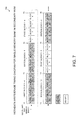
- FIG. 7 shows a metadata write/erase timing diagram 700 for a single memory bank in a secondary NVM in accordance with one embodiment of the invention.
- timing diagram 700 shows write/erase timing for secondary NVM memory bank 1 from time T 0 through time T 6 .
- the secondary NVM memory bank 1 comprises blocks 1 - 12 for storing metadata, wherein a block that is written with metadata is indicated by a shaded rectangle and a block that is erased is indicated by a clear rectangle.
- Each block may have a metadata storage capacity of 32 KB, 64 KB, 256 KB, or greater, for example.
- metadata in the secondary NVM 106 is erased after metadata has been written to the secondary NVM 106 according to a predetermined block ration of metadata erased to metadata written.
- blocks 1 - 4 are written from time T 0 -T 1
- blocks 5 - 8 are written from time T 1 -T 2
- blocks 1 - 4 are erased from time T 2 -T 3
- blocks 9 - 12 are written from time T 3 -T 4
- blocks 5 - 8 are erased from time T 4 -T 5
- blocks 1 - 4 are written from time T 5 -T 6 , and so forth.
- two groups of four blocks each (blocks 1 - 4 and blocks 5 - 8 ) are written, followed by an alternating pattern of erasing and writing a group of four blocks.
- a different number of blocks in a memory bank in a secondary NVM may be written before any blocks are erased.
- all of the blocks in a bank of memory in a secondary NVM may be written, and then all of the blocks may be erased before any of the blocks are rewritten.
- FIG. 8 shows a metadata write/erase timing diagram 800 for two memory banks in a secondary NVM in accordance with one embodiment of the invention.
- secondary NVM memory banks 1 and 2 each comprise four blocks for storing metadata, in which the four blocks are written and erased in groups of two blocks.
- a written block is indicated by a shaded block
- an erased block is written by a clear block
- an idle state of a memory bank is indicated by a cross-hatched pattern.
- memory banks 1 and 2 are each independently operable via, for example, a separate SPI, such that the control circuitry can write to memory bank 1 while erasing memory bank 2 , and vice versa.
- each memory bank 1 and 2 is situated in a different memory device.
- each memory bank 1 and 2 is situated in the same memory device.
- a secondary NVM may comprise more than two independently operable memory banks, wherein each memory bank comprises one or more blocks that can
- FIG. 9 shows an example of a primary NVM 906 comprising a disk 907 including zone WPs for SMR zones (e.g., drive-managed or host-managed SMR).
- the disk 907 comprises N zones for storing data, wherein a zone or a portion of a zone that is currently unused (i.e., has not been written to as yet) is indicated by a clear rectangle, and a zone or a portion of a zone that has been written to is indicated by a shaded rectangle.
- the host can beginning writing data at the beginning of an unused zone, such as zone 4 .
- a zone WP may be used to indicate the location in that zone at which the host can start writing.
- zone WP 1 , WP 2 , and WP 3 indicate the location in respective zones 1 , 2 , and 3 at which the host can start writing.
- the disk 907 further comprises a metadata storage region, which may be used for storing a zone WP location table.
- FIG. 10 shows a process 1000 for determining when to write metadata that has accumulated in a volatile memory 110 ( FIG. 1A-4A ) to a secondary NVM 106 ( FIG. 1A, 4A ), 206 , ( FIG. 2A ), 306 a , 306 b ( FIG. 3A ) in a data storage device 100 - 400 ( FIG. 1A-4A ), in accordance with one embodiment of the invention.
- the process 1000 can be implemented by the control circuitry 102 ( FIG. 1A ), 202 ( FIG. 2A ), 302 ( FIG. 3A ), 402 ( FIG. 4A ) of the data storage device 100 - 400 ( FIG.
- the process 1000 can be implemented in a data storage device 400 ( FIG. 4A ) using LBA indirection (e.g., SMR) for writing data in a primary NVM 404 ( FIG. 4A ) comprising a disk 424 ( FIG. 4A ).
- LBA indirection e.g., SMR
- the process 1000 can be implemented in a data storage device comprising a primary NVM 506 ( FIG. 5 ) comprising a disk 507 comprising an MBC 513 ( FIG. 5 ).
- the process 1000 may begin when a write command is received from a host.
- the process 1000 starts in block 1002 where, for each host write command received, any associated metadata is written to the volatile memory.
- the metadata may comprise, for example, a mapping table update, such as an update for a MBC mapping table.
- the process 1000 determines if the amount of metadata in the volatile memory is greater than a predetermined amount.
- the predetermined amount of metadata is the amount of metadata corresponding to a predetermined number of mapping table updates to a mapping table.
- the predetermined amount of metadata is the amount of metadata in the volatile memory that is safe via an egress process (as previously described) from an unexpected power loss (e.g., the amount of metadata that power safe region 112 of the volatile memory 110 can hold).
- the process 1000 determines that the amount of metadata in the volatile memory is not greater than the predetermined amount, and the process 1000 determines in block 1006 that the host write commands are not idle, the process returns to block 1002 .
- the process 1000 determines in block 1008 if the time since the last metadata write to the secondary NVM is greater than a predetermined duration, and if so, the process 1000 writes in block 1010 the accumulated metadata in the volatile memory to the secondary NVM.
- the predetermined duration is based on a rate of metadata generated relative to a throughput of the secondary NVM.
- the predetermined duration corresponds to a time required to write user data to a predetermined amount of data tracks in a primary NVM 404 ( FIG. 4 ) (a disk 424 ) in the data storage device 400 ( FIG. 4 ).
- the process 1000 continues to execute block 1008 until the time since the last metadata write to the secondary NVM is greater than the predetermined duration.
- FIG. 11 shows a process 1100 for determining when to erase an oldest block of metadata in a secondary NVM 106 ( FIG. 1A, 4A ), 206 , ( FIG. 2A ), 306 a , 306 b ( FIG. 3A ) in a data storage device 100 - 400 ( FIG. 1A-4A ), in accordance with one embodiment of the invention.
- the process 1100 can be implemented by the control circuitry 102 ( FIG. 1A ), 202 ( FIG. 2A ), 302 ( FIG. 3A ), 402 ( FIG. 4A ) of the data storage device 100 - 400 ( FIG. 1A-4A ) (e.g., an HDD or an SSHD).
- the process 1100 begins at block 1102 , where a predetermined amount of metadata is written from a volatile memory 110 ( FIG. 1A-4A ) to the secondary NVM.
- the metadata may comprise, for example, a mapping table update.
- the predetermined amount of metadata corresponds to a predetermined number of memory units (e.g., pages) of a predetermined size (e.g., 14 ⁇ 256B pages of metadata) comprising mapping table updates.
- the process 1100 increments a metadata count, and in block 1106 the process determines if the metadata count is greater than or equal to N.
- the process exits; and when the metadata count is greater than or equal to N, the process in block 1108 erases the oldest block of metadata in the secondary NVM, and in block 1110 , sets the metadata count equal to 0 and exits.
- the process continues to repeat blocks 1102 , 1104 , and 1106 until the process 1100 determines that the metadata count is greater than or equal to N, and then executes blocks 1108 and 1100 and exits.
- FIG. 12 shows a process 1200 for determining when to write metadata (e.g., mapping and zone WP location table updates) that has accumulated in a volatile memory 110 ( FIG. 1A-4A ) to a secondary NVM 106 ( FIG. 1A, 4A ), 206 , ( FIG. 2A ), 306 a , 306 b ( FIG. 3A ) in a data storage device 100 - 400 ( FIG. 1A-4A ) that uses LBA indirection (e.g., drive-managed SMR) for writing data in a primary NVM 104 - 404 ( FIG. 1A-4A ), in accordance with one embodiment of the invention.
- the process 1200 can be implemented by the control circuitry 102 ( FIG. 1A ), 202 ( FIG. 2A ), 302 ( FIG. 3A ), 402 ( FIG. 4A ) of the data storage device 100 - 400 ( FIG. 1A-4A ) (e.g., an HDD or SSHD).
- metadata
- the process 1200 begins in block 1202 , where the process 1200 determines if a recovery procedure from an unexpected power loss is being implemented, and if the recovery procedure is being implemented, the process 1200 reads all the metadata from the primary and the secondary NVM. In one embodiment, the process 1200 reads all mapping and zone WP location table metadata from a metadata storage region of the primary NVM and mapping and zone WP location table update metadata from the secondary NVM. In block 1206 , the process 1200 merges the metadata from the secondary and primary NVM to form updated metadata, writes the updated metadata to the primary NVM in block 1208 , and erases all the metadata from the secondary NVM in block 1210 .
- the process 1200 in FIG. 12 proceeds to block 1212 , where the process 1200 reads the mapping table and zone WP location table metadata from the metadata region of the primary NVM, and in block 1214 the process 1200 creates dynamic mapping and zone WP location tables in the volatile memory.
- the process 1200 determines if a write command is received from the host, and if not, the process 1200 continues to execute block 1216 until a host write command is received.
- the process 1200 updates in block 1218 the dynamic mapping and zone WP tables in the volatile memory with updated mapping and zone WP table metadata associated with the host write command.
- the process determines if the updated metadata that has accumulated in the volatile memory is power safe (i.e., whether the accumulated metadata is protected by an egress process (as previously described) after an occurrence of an unexpected power loss.
- the accumulated metadata in the volatile memory is safe from an unexpected power loss if it resides in the power-safe region 112 of the volatile memory 110 . If the process 1200 determines that the accumulated metadata in the volatile memory is power safe, the process 1200 determines in block 1222 if an unexpected power loss is occurring, and if not, the process 1200 proceeds to block 1216 to determine if a host write command is being received. If the process 1200 determines that an unexpected power loss is occurring, the process 1200 writes in block 1224 the dynamic updated mapping and zone WP location tables in the volatile memory to the secondary NVM via an egress process and exits.
- the process 1200 determines in block 1226 if space is available in the secondary NVM, and if so the process 1200 writes in block 1228 the portion of the updated metadata in the volatile memory that is not power safe to the secondary NVM and executes block 1216 again. If the process 1200 determines that there is not sufficient space available in the secondary NVM, the process 1200 writes in block 1230 all updated metadata in the volatile memory to the primary NVM, erases in block 1232 all the metadata from the secondary NVM, and executes block 1216 again.
- FIG. 13 shows a process 1300 for determining when to write metadata (e.g., zone WP location table updates) that has accumulated in a volatile memory 110 ( FIG. 1A-4A ) to a secondary NVM 106 ( FIG. 1A, 4A ), 206 , ( FIG. 2A ), 306 a , 306 b ( FIG. 3A ) in a data storage device 100 - 400 ( FIG. 1A-4A ) that utilizes host-managed, full LBA indirection (e.g., SMR) for writing data in a primary NVM 104 - 404 ( FIG. 1A-4A ), 906 ( FIG. 9 ), in accordance with one embodiment of the invention.
- metadata e.g., zone WP location table updates
- the process 1300 can be implemented by the control circuitry 102 ( FIG. 1A ), 202 ( FIG. 2A ), 302 ( FIG. 3A ), 402 ( FIG. 4A ) of the data storage device 100 - 400 ( FIG. 1A-4A ) (e.g., an HDD or an SSHD).
- the control circuitry 102 FIG. 1A
- 202 FIG. 2A
- 302 FIG. 3A
- 402 FIG. 4A
- the data storage device 100 - 400 FIG. 1A-4A
- FIG. 1A-4A e.g., an HDD or an SSHD
- blocks 1312 - 1332 are similar to respective blocks 1212 - 1232 in process 1200 in FIG. 12 , with a difference being that the metadata referred to in process 1300 in FIG. 13 comprises zone WP location table updates, while the metadata referred to in process 1200 in FIG. 12 comprises mapping and zone WP location table updates.
- the execution of blocks 1312 - 1332 of process 1300 in FIG. 13 will not be discussed.
- FIG. 14 shows a process 1400 for determining when to write metadata (e.g., mapping table updates) that has accumulated in a volatile memory 110 ( FIG. 1A-4A ) to a secondary NVM 106 ( FIG. 1A, 4A ), 206 , ( FIG. 2A ), 306 a , 306 b ( FIG. 3A ) in a data storage device 100 - 400 ( FIG. 1A-4A ) that utilizes LBA indirection for writing data in an MBC in a primary NVM (e.g., MBC 513 in primary NVM 506 in FIG. 5 ), in accordance with one embodiment of the invention.
- the process 1400 may be implemented by the control circuitry 102 ( FIG. 1A ), 202 ( FIG. 2A ), 302 ( FIG. 3A ), 402 ( FIG. 4A ) of the data storage device 100 - 400 ( FIG. 1A-4A ) (e.g., an HDD or an SSHD).
- metadata e.g.
- the process 1400 in FIG. 14 begins at block 1402 , where the process 1400 reads a mapping table from the metadata storage region 515 ( FIG. 5 ) of a disk 506 (the primary NVM), and creates in block 1404 a dynamic mapping table in the volatile memory.
- the process 1400 determines if a write command is received from the host, and if not, the process 1400 continues to execute block 1406 until a host write command is received.
- the process 1400 updates in block 1408 the dynamic mapping table in the volatile memory with updated mapping table metadata associated with the host write command.
- the process 1400 determines if mapping table updates have been completed for a target number of data tracks in the disk 507 ( FIG. 5 ) (the primary NVM), and if so, the process 1400 determines in block 1412 if enough time has expired to write to the secondary NVM at a safe speed. If the process 1400 determines that enough time has not expired to write to the secondary NVM at a safe speed, or the process 1400 determines in block 1410 that updates for a target number of tracks has not been completed, the process determines in block 1414 if an unexpected power loss is occurring, and if not, the process 1400 proceeds to block 1406 in which to determine if a host write command is being received. If the process 1400 determines that an unexpected power loss is occurring, the process 1400 writes in block 1416 the dynamic updated mapping table in the volatile memory to the secondary NVM via an egress process (as previously described) and exits.
- the process 1400 determines in block 1418 if space is available in the secondary NVM, and if so the process 1400 writes in block 1420 the updated mapping table metadata in the volatile memory to the secondary NVM and executes block 1406 again. If the process 1400 determines that there is not sufficient space available in the secondary NVM, the process 1400 writes in block 1422 all updated metadata in the volatile memory to the primary NVM, erases, in block 1424 , all the metadata in the secondary NVM, and executes block 1406 again.
- control circuitry 102 may be employed in the embodiments of the invention, such as any suitable integrated circuit or circuits.
- the control circuitry may be implemented within a read channel integrated circuit, or in a component separate from the read channel, such as a disk controller, or certain blocks described above may be performed by a read channel and others by a disk controller.
- the read channel and disk controller are implemented as separate integrated circuits, and in an alternative embodiment they are fabricated into a single integrated circuit or SOC.
- the control circuitry may include a suitable preamp circuit implemented as a separate integrated circuit, integrated into the read channel or disk controller circuit, or integrated into an SOC.
- control circuitry comprises a microprocessor executing instructions, the instructions being operable to cause the microprocessor to perform the blocks in the flow diagrams described herein.
- the instructions may be stored in any computer-readable medium. In one embodiment, they may be stored on a non-volatile semiconductor memory external to the microprocessor, or integrated with the microprocessor in a SOC. In another embodiment, the instructions are stored on the disk 424 ( FIG. 4A ) and read into a volatile memory 110 ( FIG. 1A-4A ) when the disk drive is powered on. In yet another embodiment, the control circuitry comprises suitable logic circuitry, such as state machine circuitry.
Landscapes
- Engineering & Computer Science (AREA)
- Theoretical Computer Science (AREA)
- Physics & Mathematics (AREA)
- General Engineering & Computer Science (AREA)
- General Physics & Mathematics (AREA)
- Human Computer Interaction (AREA)
- Quality & Reliability (AREA)
- Computer Security & Cryptography (AREA)
- Signal Processing For Digital Recording And Reproducing (AREA)
Abstract
Description
Claims (26)
Priority Applications (1)
| Application Number | Priority Date | Filing Date | Title |
|---|---|---|---|
| US14/870,571 US9836232B1 (en) | 2015-09-30 | 2015-09-30 | Data storage device and method for using secondary non-volatile memory for temporary metadata storage |
Applications Claiming Priority (1)
| Application Number | Priority Date | Filing Date | Title |
|---|---|---|---|
| US14/870,571 US9836232B1 (en) | 2015-09-30 | 2015-09-30 | Data storage device and method for using secondary non-volatile memory for temporary metadata storage |
Publications (1)
| Publication Number | Publication Date |
|---|---|
| US9836232B1 true US9836232B1 (en) | 2017-12-05 |
Family
ID=60452205
Family Applications (1)
| Application Number | Title | Priority Date | Filing Date |
|---|---|---|---|
| US14/870,571 Active 2036-04-15 US9836232B1 (en) | 2015-09-30 | 2015-09-30 | Data storage device and method for using secondary non-volatile memory for temporary metadata storage |
Country Status (1)
| Country | Link |
|---|---|
| US (1) | US9836232B1 (en) |
Cited By (28)
| Publication number | Priority date | Publication date | Assignee | Title |
|---|---|---|---|---|
| US9997194B1 (en) * | 2017-09-25 | 2018-06-12 | Amazon Technologies, Inc. | Partial updates for shingled magnetic recording devices |
| US20190220402A1 (en) * | 2018-01-18 | 2019-07-18 | EMC IP Holding Company LLC | Data recovery method, data recovery system, and computer program product |
| US10684954B2 (en) * | 2015-04-02 | 2020-06-16 | Hewlett Packard Enterprise Development Lp | Page cache on persistent memory |
| US10719118B2 (en) * | 2018-05-11 | 2020-07-21 | International Business Machines Corporation | Power level management in a data storage system |
| US10824362B2 (en) | 2015-03-27 | 2020-11-03 | Hewlett Packard Enterprise Development Lp | File migration to persistent memory |
| US10824342B2 (en) | 2014-02-28 | 2020-11-03 | Hewlett Packard Enterprise Development Lp | Mapping mode shift between mapping modes that provides continuous application access to storage, wherein address range is remapped between said modes during data migration and said address range is also utilized bypass through instructions for direct access |
| US10990526B1 (en) * | 2020-04-30 | 2021-04-27 | Micron Technology, Inc. | Handling asynchronous power loss in a memory sub-system that programs sequentially |
| US11126378B1 (en) | 2020-05-27 | 2021-09-21 | Western Digital Technologies, Inc. | Rate limit on the transitions of zones to open |
| US11194521B1 (en) | 2020-05-27 | 2021-12-07 | Western Digital Technologies, Inc. | Rate limit on the transitions of streams to open |
| US20220035552A1 (en) * | 2020-07-31 | 2022-02-03 | Kioxia Corporation | Ssd supporting read-only mode after plp backup failure |
| US11269778B1 (en) * | 2020-11-17 | 2022-03-08 | Micron Technology, Inc. | Mapping supporting non-sequential writes at sequentially-written memory devices |
| US11379127B2 (en) | 2019-07-18 | 2022-07-05 | Alibaba Group Holding Limited | Method and system for enhancing a distributed storage system by decoupling computation and network tasks |
| US11379447B2 (en) * | 2020-02-06 | 2022-07-05 | Alibaba Group Holding Limited | Method and system for enhancing IOPS of a hard disk drive system based on storing metadata in host volatile memory and data in non-volatile memory using a shared controller |
| US11385833B2 (en) | 2020-04-20 | 2022-07-12 | Alibaba Group Holding Limited | Method and system for facilitating a light-weight garbage collection with a reduced utilization of resources |
| US20220276789A1 (en) * | 2021-02-26 | 2022-09-01 | Micron Technology, Inc. | Effective storage allocation for sequentially-written memory devices |
| US11449386B2 (en) | 2020-03-20 | 2022-09-20 | Alibaba Group Holding Limited | Method and system for optimizing persistent memory on data retention, endurance, and performance for host memory |
| US11449455B2 (en) | 2020-01-15 | 2022-09-20 | Alibaba Group Holding Limited | Method and system for facilitating a high-capacity object storage system with configuration agility and mixed deployment flexibility |
| US11487465B2 (en) | 2020-12-11 | 2022-11-01 | Alibaba Group Holding Limited | Method and system for a local storage engine collaborating with a solid state drive controller |
| US11507499B2 (en) | 2020-05-19 | 2022-11-22 | Alibaba Group Holding Limited | System and method for facilitating mitigation of read/write amplification in data compression |
| US11556277B2 (en) | 2020-05-19 | 2023-01-17 | Alibaba Group Holding Limited | System and method for facilitating improved performance in ordering key-value storage with input/output stack simplification |
| US11617282B2 (en) | 2019-10-01 | 2023-03-28 | Alibaba Group Holding Limited | System and method for reshaping power budget of cabinet to facilitate improved deployment density of servers |
| US11726699B2 (en) | 2021-03-30 | 2023-08-15 | Alibaba Singapore Holding Private Limited | Method and system for facilitating multi-stream sequential read performance improvement with reduced read amplification |
| US11734115B2 (en) | 2020-12-28 | 2023-08-22 | Alibaba Group Holding Limited | Method and system for facilitating write latency reduction in a queue depth of one scenario |
| US11768709B2 (en) | 2019-01-02 | 2023-09-26 | Alibaba Group Holding Limited | System and method for offloading computation to storage nodes in distributed system |
| US11816043B2 (en) | 2018-06-25 | 2023-11-14 | Alibaba Group Holding Limited | System and method for managing resources of a storage device and quantifying the cost of I/O requests |
| US20240103745A1 (en) * | 2022-09-28 | 2024-03-28 | Advanced Micro Devices, Inc. | Scheduling Processing-in-Memory Requests and Memory Requests |
| US12131026B2 (en) | 2022-12-29 | 2024-10-29 | Advanced Micro Devices, Inc. | Adaptive scheduling of memory and processing-in-memory requests |
| US12236134B2 (en) | 2022-09-27 | 2025-02-25 | Advanced Micro Devices, Inc. | Bank-level parallelism for processing in memory |
Citations (93)
| Publication number | Priority date | Publication date | Assignee | Title |
|---|---|---|---|---|
| US6856556B1 (en) | 2003-04-03 | 2005-02-15 | Siliconsystems, Inc. | Storage subsystem with embedded circuit for protecting against anomalies in power signal from host |
| US20070300037A1 (en) * | 2006-06-23 | 2007-12-27 | Microsoft Corporation | Persistent flash memory mapping table |
| US20080052449A1 (en) * | 2006-08-22 | 2008-02-28 | Jin-Ki Kim | Modular command structure for memory and memory system |
| US7430136B2 (en) | 2004-11-30 | 2008-09-30 | Siliconsystems, Inc. | Purge operations for solid-state storage devices |
| US20080270730A1 (en) | 2007-04-30 | 2008-10-30 | Sandisk Il Ltd. | Method for efficient storage of metadata in flash memory |
| US7447807B1 (en) | 2006-06-30 | 2008-11-04 | Siliconsystems, Inc. | Systems and methods for storing data in segments of a storage subsystem |
| US7509441B1 (en) | 2006-06-30 | 2009-03-24 | Siliconsystems, Inc. | Systems and methods for segmenting and protecting a storage subsystem |
| US20090196102A1 (en) * | 2008-02-04 | 2009-08-06 | Mosaid Technologies Incorporated | Flexible memory operations in nand flash devices |
| US7596643B2 (en) | 2007-02-07 | 2009-09-29 | Siliconsystems, Inc. | Storage subsystem with configurable buffer |
| US7653778B2 (en) | 2006-05-08 | 2010-01-26 | Siliconsystems, Inc. | Systems and methods for measuring the useful life of solid-state storage devices |
| US20100070729A1 (en) | 2008-09-18 | 2010-03-18 | Seagate Technology Llc | System and method of managing metadata |
| US7685374B2 (en) | 2007-07-26 | 2010-03-23 | Siliconsystems, Inc. | Multi-interface and multi-bus structured solid-state storage subsystem |
| US7685338B2 (en) | 2007-05-24 | 2010-03-23 | Siliconsystems, Inc. | Solid state storage subsystem for embedded applications |
| US7685337B2 (en) | 2007-05-24 | 2010-03-23 | Siliconsystems, Inc. | Solid state storage subsystem for embedded applications |
| US7733712B1 (en) | 2008-05-20 | 2010-06-08 | Siliconsystems, Inc. | Storage subsystem with embedded circuit for protecting against anomalies in power signal from host |
| US20100174849A1 (en) | 2009-01-07 | 2010-07-08 | Siliconsystems, Inc. | Systems and methods for improving the performance of non-volatile memory operations |
| US7765373B1 (en) | 2006-06-27 | 2010-07-27 | Siliconsystems, Inc. | System for controlling use of a solid-state storage subsystem |
| US20100250793A1 (en) | 2009-03-24 | 2010-09-30 | Western Digital Technologies, Inc. | Adjusting access of non-volatile semiconductor memory based on access time |
| US20100287332A1 (en) * | 2009-05-08 | 2010-11-11 | Junichi Koshiyama | Data storing system, data storing method, executing device, control method thereof, control device, and control method thereof |
| US20100318821A1 (en) * | 2009-06-15 | 2010-12-16 | Broadcom Corporation | Scalable, dynamic power management scheme for switching architectures utilizing multiple banks |
| US20110099323A1 (en) | 2009-10-27 | 2011-04-28 | Western Digital Technologies, Inc. | Non-volatile semiconductor memory segregating sequential, random, and system data to reduce garbage collection for page based mapping |
| US7962792B2 (en) | 2008-02-11 | 2011-06-14 | Siliconsystems, Inc. | Interface for enabling a host computer to retrieve device monitor data from a solid state storage subsystem |
| US20110208914A1 (en) * | 2008-08-21 | 2011-08-25 | Infinidat Ltd. | Storage system and method of operating thereof |
| US20110276744A1 (en) * | 2010-05-05 | 2011-11-10 | Microsoft Corporation | Flash memory cache including for use with persistent key-value store |
| US20110283049A1 (en) | 2010-05-12 | 2011-11-17 | Western Digital Technologies, Inc. | System and method for managing garbage collection in solid-state memory |
| US8078918B2 (en) | 2008-02-07 | 2011-12-13 | Siliconsystems, Inc. | Solid state storage subsystem that maintains and provides access to data reflective of a failure risk |
| US8090899B1 (en) | 2009-03-04 | 2012-01-03 | Western Digital Technologies, Inc. | Solid state drive power safe wear-leveling |
| US8095851B2 (en) | 2007-09-06 | 2012-01-10 | Siliconsystems, Inc. | Storage subsystem capable of adjusting ECC settings based on monitored conditions |
| US8108692B1 (en) | 2006-06-27 | 2012-01-31 | Siliconsystems, Inc. | Solid-state storage subsystem security solution |
| US8135903B1 (en) | 2009-10-30 | 2012-03-13 | Western Digital Technologies, Inc. | Non-volatile semiconductor memory compressing data to improve performance |
| US8161227B1 (en) | 2006-10-30 | 2012-04-17 | Siliconsystems, Inc. | Storage subsystem capable of programming field-programmable devices of a target computer system |
| US8243525B1 (en) | 2009-09-30 | 2012-08-14 | Western Digital Technologies, Inc. | Refreshing non-volatile semiconductor memory by reading without rewriting |
| US8254172B1 (en) | 2009-09-30 | 2012-08-28 | Western Digital Technologies, Inc. | Wear leveling non-volatile semiconductor memory based on erase times and program times |
| US8261012B2 (en) | 2009-10-30 | 2012-09-04 | Western Digital Technologies, Inc. | Non-volatile semiconductor memory comprising power fail circuitry for flushing write data in response to a power fail signal |
| US20120260020A1 (en) | 2011-04-06 | 2012-10-11 | Western Digital Technologies, Inc. | Non-volatile semiconductor memory module enabling out of order host command chunk media access |
| US20120278531A1 (en) | 2011-04-29 | 2012-11-01 | Western Digital Technologies, Inc. | System and method for improved parity determination within a data redundancy scheme in a solid state memory |
| US20120284460A1 (en) | 2011-05-02 | 2012-11-08 | Western Digital Technologies, Inc. | High performance path for command processing |
| US8316176B1 (en) | 2010-02-17 | 2012-11-20 | Western Digital Technologies, Inc. | Non-volatile semiconductor memory segregating sequential data during garbage collection to reduce write amplification |
| US20120324191A1 (en) | 2011-06-14 | 2012-12-20 | Western Digital Technologies, Inc. | System and method for performing data retention that incorporates environmental conditions |
| US8341339B1 (en) | 2010-06-14 | 2012-12-25 | Western Digital Technologies, Inc. | Hybrid drive garbage collecting a non-volatile semiconductor memory by migrating valid data to a disk |
| US8375151B1 (en) | 2009-02-12 | 2013-02-12 | Siliconsystems, Inc. | Command portal for securely communicating and executing non-standard storage subsystem commands |
| US20130046918A1 (en) | 2011-08-18 | 2013-02-21 | Samsung Electronics Co., Ltd. | Method writing meta data with reduced frequency |
| US8392635B2 (en) | 2010-12-22 | 2013-03-05 | Western Digital Technologies, Inc. | Selectively enabling a host transfer interrupt |
| US8397107B1 (en) | 2009-12-11 | 2013-03-12 | Western Digital Technologies, Inc. | Data storage device employing data path protection using both LBA and PBA |
| US20130073816A1 (en) | 2011-09-19 | 2013-03-21 | Samsung Electronics Co.,Ltd. | Method of storing data in a storage medium and data storage device including the storage medium |
| US8407449B1 (en) | 2010-02-26 | 2013-03-26 | Western Digital Technologies, Inc. | Non-volatile semiconductor memory storing an inverse map for rebuilding a translation table |
| US8423722B1 (en) | 2011-08-26 | 2013-04-16 | Western Digital Technologies, Inc. | System and method for high performance command processing in solid state drives |
| US8443167B1 (en) | 2009-12-16 | 2013-05-14 | Western Digital Technologies, Inc. | Data storage device employing a run-length mapping table and a single address mapping table |
| US8447920B1 (en) | 2010-06-29 | 2013-05-21 | Western Digital Technologies, Inc. | System and method for managing data access in non-volatile memory |
| US20130132638A1 (en) | 2011-11-21 | 2013-05-23 | Western Digital Technologies, Inc. | Disk drive data caching using a multi-tiered memory |
| US8458435B1 (en) | 2010-12-20 | 2013-06-04 | Western Digital Technologies, Inc. | Sequential write thread detection |
| US8503237B1 (en) | 2011-05-18 | 2013-08-06 | Western Digital Technologies, Inc. | System and method for data recovery in a solid state storage device |
| US8521972B1 (en) | 2010-06-30 | 2013-08-27 | Western Digital Technologies, Inc. | System and method for optimizing garbage collection in data storage |
| US20130227206A1 (en) | 2010-11-04 | 2013-08-29 | Micron Technology, Inc. | Metadata storage associated with wear-level operation requests |
| US8549236B2 (en) | 2006-12-15 | 2013-10-01 | Siliconsystems, Inc. | Storage subsystem with multiple non-volatile memory arrays to protect against data losses |
| US20130290793A1 (en) | 2012-04-25 | 2013-10-31 | Western Digital Technologies, Inc. | Managing unreliable memory in data storage systems |
| US8583835B1 (en) | 2008-08-06 | 2013-11-12 | Siliconsystems, Inc. | Command portal for executing non-standard storage subsystem commands |
| US8601313B1 (en) | 2010-12-13 | 2013-12-03 | Western Digital Technologies, Inc. | System and method for a data reliability scheme in a solid state memory |
| US8601311B2 (en) | 2010-12-14 | 2013-12-03 | Western Digital Technologies, Inc. | System and method for using over-provisioned data capacity to maintain a data redundancy scheme in a solid state memory |
| US8612804B1 (en) | 2010-09-30 | 2013-12-17 | Western Digital Technologies, Inc. | System and method for improving wear-leveling performance in solid-state memory |
| US8612669B1 (en) | 2010-06-28 | 2013-12-17 | Western Digital Technologies, Inc. | System and method for performing data retention in solid-state memory using copy commands and validity and usage data |
| US8615681B2 (en) | 2010-12-14 | 2013-12-24 | Western Digital Technologies, Inc. | System and method for maintaining a data redundancy scheme in a solid state memory in the event of a power loss |
| US8639872B1 (en) | 2010-08-13 | 2014-01-28 | Western Digital Technologies, Inc. | Hybrid drive comprising write cache spanning non-volatile semiconductor memory and disk |
| US8638602B1 (en) | 2010-09-10 | 2014-01-28 | Western Digital Technologies, Inc. | Background selection of voltage reference values for performing memory read operations |
| US20140059405A1 (en) | 2012-08-21 | 2014-02-27 | Western Digital Technologies, Inc. | Solid-state drive retention monitor using reference blocks |
| US8683113B2 (en) | 2011-02-04 | 2014-03-25 | Western Digital Technologies, Inc. | Concurrently searching multiple devices of a non-volatile semiconductor memory |
| US20140101369A1 (en) | 2012-10-05 | 2014-04-10 | Western Digital Technologies, Inc. | Methods, devices and systems for physical-to-logical mapping in solid state drives |
| US8700834B2 (en) | 2011-09-06 | 2014-04-15 | Western Digital Technologies, Inc. | Systems and methods for an enhanced controller architecture in data storage systems |
| US8700950B1 (en) | 2011-02-11 | 2014-04-15 | Western Digital Technologies, Inc. | System and method for data error recovery in a solid state subsystem |
| US8700951B1 (en) | 2011-03-09 | 2014-04-15 | Western Digital Technologies, Inc. | System and method for improving a data redundancy scheme in a solid state subsystem with additional metadata |
| US8707104B1 (en) | 2011-09-06 | 2014-04-22 | Western Digital Technologies, Inc. | Systems and methods for error injection in data storage systems |
| US20140115427A1 (en) | 2012-10-24 | 2014-04-24 | Western Digital Technologies, Inc. | Adaptive error correction codes for data storage systems |
| US8713066B1 (en) | 2010-03-29 | 2014-04-29 | Western Digital Technologies, Inc. | Managing wear leveling and garbage collection operations in a solid-state memory using linked lists |
| US8713357B1 (en) | 2011-09-06 | 2014-04-29 | Western Digital Technologies, Inc. | Systems and methods for detailed error reporting in data storage systems |
| US8725931B1 (en) | 2010-03-26 | 2014-05-13 | Western Digital Technologies, Inc. | System and method for managing the execution of memory commands in a solid-state memory |
| US8724422B1 (en) | 2012-02-29 | 2014-05-13 | Western Digital Technologies, Inc. | System and method for charging back-up charge storage element for data storage device using spindle phase switching elements |
| US20140136753A1 (en) | 2012-11-15 | 2014-05-15 | Western Digital Technologies, Inc. | Methods, data storage devices and systems for fragmented firmware table rebuild in a solid state drive |
| US20140133220A1 (en) | 2012-11-13 | 2014-05-15 | Western Digital Technologies, Inc. | Methods and devices for avoiding lower page corruption in data storage devices |
| US20140149826A1 (en) | 2012-11-29 | 2014-05-29 | Western Digital Technologies, Inc. | Data reliability schemes for data storage systems |
| US20140157078A1 (en) | 2012-12-03 | 2014-06-05 | Western Digital Technologies, Inc. | Methods, solid state drive controllers and data storage devices having a runtime variable raid protection scheme |
| US8751728B1 (en) | 2011-04-29 | 2014-06-10 | Western Digital Technologies, Inc. | Storage system bus transfer optimization |
| US20140164675A1 (en) * | 2012-12-06 | 2014-06-12 | Richard M. Ehrlich | Low-overhead storage of a hibernation file in a hybrid disk drive |
| US20140181432A1 (en) | 2012-12-26 | 2014-06-26 | Western Digital Technologies, Inc. | Priority-based garbage collection for data storage systems |
| US8769190B1 (en) | 2010-09-15 | 2014-07-01 | Western Digital Technologies, Inc. | System and method for reducing contentions in solid-state memory access |
| US8775720B1 (en) | 2010-08-31 | 2014-07-08 | Western Digital Technologies, Inc. | Hybrid drive balancing execution times for non-volatile semiconductor memory and disk |
| US8782327B1 (en) | 2010-05-11 | 2014-07-15 | Western Digital Technologies, Inc. | System and method for managing execution of internal commands and host commands in a solid-state memory |
| US8788779B1 (en) | 2010-09-17 | 2014-07-22 | Western Digital Technologies, Inc. | Non-volatile storage subsystem with energy-based performance throttling |
| US8788880B1 (en) | 2012-08-22 | 2014-07-22 | Western Digital Technologies, Inc. | Efficient retry mechanism for solid-state memory failures |
| US8788778B1 (en) | 2012-06-04 | 2014-07-22 | Western Digital Technologies, Inc. | Garbage collection based on the inactivity level of stored data |
| US8793429B1 (en) | 2011-06-03 | 2014-07-29 | Western Digital Technologies, Inc. | Solid-state drive with reduced power up time |
| US20140223121A1 (en) * | 2013-02-05 | 2014-08-07 | International Business Machines Corporation | Point in time copy operations from source volumes to space efficient target volumes in two stages via a non-volatile storage |
| US20140223255A1 (en) | 2012-12-18 | 2014-08-07 | Western Digital Technologies, Inc. | Decoder having early decoding termination detection |
| US20150095572A1 (en) * | 2012-06-25 | 2015-04-02 | Fujitsu Limited | Storage control apparatus and storage control method |
-
2015
- 2015-09-30 US US14/870,571 patent/US9836232B1/en active Active
Patent Citations (112)
| Publication number | Priority date | Publication date | Assignee | Title |
|---|---|---|---|---|
| US7126857B2 (en) | 2003-04-03 | 2006-10-24 | Siliconsystems, Inc. | Storage subsystem with embedded circuit for protecting against anomalies in power signal from host |
| US6856556B1 (en) | 2003-04-03 | 2005-02-15 | Siliconsystems, Inc. | Storage subsystem with embedded circuit for protecting against anomalies in power signal from host |
| US7502256B2 (en) | 2004-11-30 | 2009-03-10 | Siliconsystems, Inc. | Systems and methods for reducing unauthorized data recovery from solid-state storage devices |
| US7898855B2 (en) | 2004-11-30 | 2011-03-01 | Siliconsystems, Inc. | Systems and methods for reducing unauthorized data recovery from solid-state storage devices |
| US7430136B2 (en) | 2004-11-30 | 2008-09-30 | Siliconsystems, Inc. | Purge operations for solid-state storage devices |
| US7936603B2 (en) | 2004-11-30 | 2011-05-03 | Siliconsystems, Inc. | Purge operations for solid-state storage devices |
| US8122185B2 (en) | 2006-05-08 | 2012-02-21 | Siliconsystems, Inc. | Systems and methods for measuring the useful life of solid-state storage devices |
| US7653778B2 (en) | 2006-05-08 | 2010-01-26 | Siliconsystems, Inc. | Systems and methods for measuring the useful life of solid-state storage devices |
| US8312207B2 (en) | 2006-05-08 | 2012-11-13 | Siliconsystems, Inc. | Systems and methods for measuring the useful life of solid-state storage devices |
| US20070300037A1 (en) * | 2006-06-23 | 2007-12-27 | Microsoft Corporation | Persistent flash memory mapping table |
| US8108692B1 (en) | 2006-06-27 | 2012-01-31 | Siliconsystems, Inc. | Solid-state storage subsystem security solution |
| US7765373B1 (en) | 2006-06-27 | 2010-07-27 | Siliconsystems, Inc. | System for controlling use of a solid-state storage subsystem |
| US7447807B1 (en) | 2006-06-30 | 2008-11-04 | Siliconsystems, Inc. | Systems and methods for storing data in segments of a storage subsystem |
| US7509441B1 (en) | 2006-06-30 | 2009-03-24 | Siliconsystems, Inc. | Systems and methods for segmenting and protecting a storage subsystem |
| US8127048B1 (en) | 2006-06-30 | 2012-02-28 | Siliconsystems, Inc. | Systems and methods for segmenting and protecting a storage subsystem |
| US7912991B1 (en) | 2006-06-30 | 2011-03-22 | Siliconsystems, Inc. | Systems and methods for segmenting and protecting a storage subsystem |
| US20080052449A1 (en) * | 2006-08-22 | 2008-02-28 | Jin-Ki Kim | Modular command structure for memory and memory system |
| US8161227B1 (en) | 2006-10-30 | 2012-04-17 | Siliconsystems, Inc. | Storage subsystem capable of programming field-programmable devices of a target computer system |
| US8549236B2 (en) | 2006-12-15 | 2013-10-01 | Siliconsystems, Inc. | Storage subsystem with multiple non-volatile memory arrays to protect against data losses |
| US7596643B2 (en) | 2007-02-07 | 2009-09-29 | Siliconsystems, Inc. | Storage subsystem with configurable buffer |
| US8151020B2 (en) | 2007-02-07 | 2012-04-03 | Siliconsystems, Inc. | Storage subsystem with configurable buffer |
| US20080270730A1 (en) | 2007-04-30 | 2008-10-30 | Sandisk Il Ltd. | Method for efficient storage of metadata in flash memory |
| US7685337B2 (en) | 2007-05-24 | 2010-03-23 | Siliconsystems, Inc. | Solid state storage subsystem for embedded applications |
| US7685338B2 (en) | 2007-05-24 | 2010-03-23 | Siliconsystems, Inc. | Solid state storage subsystem for embedded applications |
| US8433858B1 (en) | 2007-07-26 | 2013-04-30 | Siliconsystems, Inc. | Multi-interface and multi-bus structured solid-state storage subsystem |
| US8166245B2 (en) | 2007-07-26 | 2012-04-24 | Siliconsystems, Inc. | Multi-interface and multi-bus structured solid-state storage subsystem |
| US7685374B2 (en) | 2007-07-26 | 2010-03-23 | Siliconsystems, Inc. | Multi-interface and multi-bus structured solid-state storage subsystem |
| US8296625B2 (en) | 2007-09-06 | 2012-10-23 | Siliconsystems, Inc. | Storage subsystem capable of adjusting ECC settings based on monitored conditions |
| US8095851B2 (en) | 2007-09-06 | 2012-01-10 | Siliconsystems, Inc. | Storage subsystem capable of adjusting ECC settings based on monitored conditions |
| US20090196102A1 (en) * | 2008-02-04 | 2009-08-06 | Mosaid Technologies Incorporated | Flexible memory operations in nand flash devices |
| US8078918B2 (en) | 2008-02-07 | 2011-12-13 | Siliconsystems, Inc. | Solid state storage subsystem that maintains and provides access to data reflective of a failure risk |
| US7962792B2 (en) | 2008-02-11 | 2011-06-14 | Siliconsystems, Inc. | Interface for enabling a host computer to retrieve device monitor data from a solid state storage subsystem |
| US7733712B1 (en) | 2008-05-20 | 2010-06-08 | Siliconsystems, Inc. | Storage subsystem with embedded circuit for protecting against anomalies in power signal from host |
| US20130145106A1 (en) | 2008-08-06 | 2013-06-06 | Western Digital Technologies, Inc. | Command portal for securely communicating and executing non-standard storage subsystem commands |
| US8583835B1 (en) | 2008-08-06 | 2013-11-12 | Siliconsystems, Inc. | Command portal for executing non-standard storage subsystem commands |
| US8745277B2 (en) | 2008-08-06 | 2014-06-03 | Siliconsystems, Inc. | Command portal for securely communicating and executing non-standard storage subsystem commands |
| US20110208914A1 (en) * | 2008-08-21 | 2011-08-25 | Infinidat Ltd. | Storage system and method of operating thereof |
| US20100070729A1 (en) | 2008-09-18 | 2010-03-18 | Seagate Technology Llc | System and method of managing metadata |
| US20100174849A1 (en) | 2009-01-07 | 2010-07-08 | Siliconsystems, Inc. | Systems and methods for improving the performance of non-volatile memory operations |
| US8375151B1 (en) | 2009-02-12 | 2013-02-12 | Siliconsystems, Inc. | Command portal for securely communicating and executing non-standard storage subsystem commands |
| US8090899B1 (en) | 2009-03-04 | 2012-01-03 | Western Digital Technologies, Inc. | Solid state drive power safe wear-leveling |
| US8478930B1 (en) | 2009-03-04 | 2013-07-02 | Western Digital Technologies, Inc. | Solid state drive power safe wear-leveling |
| US20100250793A1 (en) | 2009-03-24 | 2010-09-30 | Western Digital Technologies, Inc. | Adjusting access of non-volatile semiconductor memory based on access time |
| US20100287332A1 (en) * | 2009-05-08 | 2010-11-11 | Junichi Koshiyama | Data storing system, data storing method, executing device, control method thereof, control device, and control method thereof |
| US20100318821A1 (en) * | 2009-06-15 | 2010-12-16 | Broadcom Corporation | Scalable, dynamic power management scheme for switching architectures utilizing multiple banks |
| US8243525B1 (en) | 2009-09-30 | 2012-08-14 | Western Digital Technologies, Inc. | Refreshing non-volatile semiconductor memory by reading without rewriting |
| US8254172B1 (en) | 2009-09-30 | 2012-08-28 | Western Digital Technologies, Inc. | Wear leveling non-volatile semiconductor memory based on erase times and program times |
| US20110099323A1 (en) | 2009-10-27 | 2011-04-28 | Western Digital Technologies, Inc. | Non-volatile semiconductor memory segregating sequential, random, and system data to reduce garbage collection for page based mapping |
| US8261012B2 (en) | 2009-10-30 | 2012-09-04 | Western Digital Technologies, Inc. | Non-volatile semiconductor memory comprising power fail circuitry for flushing write data in response to a power fail signal |
| US8135903B1 (en) | 2009-10-30 | 2012-03-13 | Western Digital Technologies, Inc. | Non-volatile semiconductor memory compressing data to improve performance |
| US8397107B1 (en) | 2009-12-11 | 2013-03-12 | Western Digital Technologies, Inc. | Data storage device employing data path protection using both LBA and PBA |
| US8443167B1 (en) | 2009-12-16 | 2013-05-14 | Western Digital Technologies, Inc. | Data storage device employing a run-length mapping table and a single address mapping table |
| US8316176B1 (en) | 2010-02-17 | 2012-11-20 | Western Digital Technologies, Inc. | Non-volatile semiconductor memory segregating sequential data during garbage collection to reduce write amplification |
| US8489854B1 (en) | 2010-02-26 | 2013-07-16 | Western Digital Technologies, Inc. | Non-volatile semiconductor memory storing an inverse map for rebuilding a translation table |
| US8407449B1 (en) | 2010-02-26 | 2013-03-26 | Western Digital Technologies, Inc. | Non-volatile semiconductor memory storing an inverse map for rebuilding a translation table |
| US8725931B1 (en) | 2010-03-26 | 2014-05-13 | Western Digital Technologies, Inc. | System and method for managing the execution of memory commands in a solid-state memory |
| US8713066B1 (en) | 2010-03-29 | 2014-04-29 | Western Digital Technologies, Inc. | Managing wear leveling and garbage collection operations in a solid-state memory using linked lists |
| US20110276744A1 (en) * | 2010-05-05 | 2011-11-10 | Microsoft Corporation | Flash memory cache including for use with persistent key-value store |
| US8782327B1 (en) | 2010-05-11 | 2014-07-15 | Western Digital Technologies, Inc. | System and method for managing execution of internal commands and host commands in a solid-state memory |
| US20110283049A1 (en) | 2010-05-12 | 2011-11-17 | Western Digital Technologies, Inc. | System and method for managing garbage collection in solid-state memory |
| US8341339B1 (en) | 2010-06-14 | 2012-12-25 | Western Digital Technologies, Inc. | Hybrid drive garbage collecting a non-volatile semiconductor memory by migrating valid data to a disk |
| US8612669B1 (en) | 2010-06-28 | 2013-12-17 | Western Digital Technologies, Inc. | System and method for performing data retention in solid-state memory using copy commands and validity and usage data |
| US8447920B1 (en) | 2010-06-29 | 2013-05-21 | Western Digital Technologies, Inc. | System and method for managing data access in non-volatile memory |
| US8706985B1 (en) | 2010-06-30 | 2014-04-22 | Western Digital Technologies, Inc. | System and method for optimizing garbage collection in data storage |
| US8521972B1 (en) | 2010-06-30 | 2013-08-27 | Western Digital Technologies, Inc. | System and method for optimizing garbage collection in data storage |
| US8639872B1 (en) | 2010-08-13 | 2014-01-28 | Western Digital Technologies, Inc. | Hybrid drive comprising write cache spanning non-volatile semiconductor memory and disk |
| US8775720B1 (en) | 2010-08-31 | 2014-07-08 | Western Digital Technologies, Inc. | Hybrid drive balancing execution times for non-volatile semiconductor memory and disk |
| US8638602B1 (en) | 2010-09-10 | 2014-01-28 | Western Digital Technologies, Inc. | Background selection of voltage reference values for performing memory read operations |
| US8769190B1 (en) | 2010-09-15 | 2014-07-01 | Western Digital Technologies, Inc. | System and method for reducing contentions in solid-state memory access |
| US8788779B1 (en) | 2010-09-17 | 2014-07-22 | Western Digital Technologies, Inc. | Non-volatile storage subsystem with energy-based performance throttling |
| US8612804B1 (en) | 2010-09-30 | 2013-12-17 | Western Digital Technologies, Inc. | System and method for improving wear-leveling performance in solid-state memory |
| US20130227206A1 (en) | 2010-11-04 | 2013-08-29 | Micron Technology, Inc. | Metadata storage associated with wear-level operation requests |
| US8601313B1 (en) | 2010-12-13 | 2013-12-03 | Western Digital Technologies, Inc. | System and method for a data reliability scheme in a solid state memory |
| US8601311B2 (en) | 2010-12-14 | 2013-12-03 | Western Digital Technologies, Inc. | System and method for using over-provisioned data capacity to maintain a data redundancy scheme in a solid state memory |
| US8615681B2 (en) | 2010-12-14 | 2013-12-24 | Western Digital Technologies, Inc. | System and method for maintaining a data redundancy scheme in a solid state memory in the event of a power loss |
| US8458435B1 (en) | 2010-12-20 | 2013-06-04 | Western Digital Technologies, Inc. | Sequential write thread detection |
| US8392635B2 (en) | 2010-12-22 | 2013-03-05 | Western Digital Technologies, Inc. | Selectively enabling a host transfer interrupt |
| US8683113B2 (en) | 2011-02-04 | 2014-03-25 | Western Digital Technologies, Inc. | Concurrently searching multiple devices of a non-volatile semiconductor memory |
| US8700950B1 (en) | 2011-02-11 | 2014-04-15 | Western Digital Technologies, Inc. | System and method for data error recovery in a solid state subsystem |
| US8700951B1 (en) | 2011-03-09 | 2014-04-15 | Western Digital Technologies, Inc. | System and method for improving a data redundancy scheme in a solid state subsystem with additional metadata |
| US8769232B2 (en) | 2011-04-06 | 2014-07-01 | Western Digital Technologies, Inc. | Non-volatile semiconductor memory module enabling out of order host command chunk media access |
| US20120260020A1 (en) | 2011-04-06 | 2012-10-11 | Western Digital Technologies, Inc. | Non-volatile semiconductor memory module enabling out of order host command chunk media access |
| US8751728B1 (en) | 2011-04-29 | 2014-06-10 | Western Digital Technologies, Inc. | Storage system bus transfer optimization |
| US20120278531A1 (en) | 2011-04-29 | 2012-11-01 | Western Digital Technologies, Inc. | System and method for improved parity determination within a data redundancy scheme in a solid state memory |
| US20120284460A1 (en) | 2011-05-02 | 2012-11-08 | Western Digital Technologies, Inc. | High performance path for command processing |
| US8503237B1 (en) | 2011-05-18 | 2013-08-06 | Western Digital Technologies, Inc. | System and method for data recovery in a solid state storage device |
| US8793429B1 (en) | 2011-06-03 | 2014-07-29 | Western Digital Technologies, Inc. | Solid-state drive with reduced power up time |
| US8719531B2 (en) | 2011-06-14 | 2014-05-06 | Western Digital Technologies, Inc. | System and method for performing data retention that incorporates environmental conditions |
| US20120324191A1 (en) | 2011-06-14 | 2012-12-20 | Western Digital Technologies, Inc. | System and method for performing data retention that incorporates environmental conditions |
| US20130046918A1 (en) | 2011-08-18 | 2013-02-21 | Samsung Electronics Co., Ltd. | Method writing meta data with reduced frequency |
| US8423722B1 (en) | 2011-08-26 | 2013-04-16 | Western Digital Technologies, Inc. | System and method for high performance command processing in solid state drives |
| US8707104B1 (en) | 2011-09-06 | 2014-04-22 | Western Digital Technologies, Inc. | Systems and methods for error injection in data storage systems |
| US8713357B1 (en) | 2011-09-06 | 2014-04-29 | Western Digital Technologies, Inc. | Systems and methods for detailed error reporting in data storage systems |
| US8700834B2 (en) | 2011-09-06 | 2014-04-15 | Western Digital Technologies, Inc. | Systems and methods for an enhanced controller architecture in data storage systems |
| US20130073816A1 (en) | 2011-09-19 | 2013-03-21 | Samsung Electronics Co.,Ltd. | Method of storing data in a storage medium and data storage device including the storage medium |
| US20130132638A1 (en) | 2011-11-21 | 2013-05-23 | Western Digital Technologies, Inc. | Disk drive data caching using a multi-tiered memory |
| US8724422B1 (en) | 2012-02-29 | 2014-05-13 | Western Digital Technologies, Inc. | System and method for charging back-up charge storage element for data storage device using spindle phase switching elements |
| US20130290793A1 (en) | 2012-04-25 | 2013-10-31 | Western Digital Technologies, Inc. | Managing unreliable memory in data storage systems |
| US8788778B1 (en) | 2012-06-04 | 2014-07-22 | Western Digital Technologies, Inc. | Garbage collection based on the inactivity level of stored data |
| US20150095572A1 (en) * | 2012-06-25 | 2015-04-02 | Fujitsu Limited | Storage control apparatus and storage control method |
| US20140059405A1 (en) | 2012-08-21 | 2014-02-27 | Western Digital Technologies, Inc. | Solid-state drive retention monitor using reference blocks |
| US8788880B1 (en) | 2012-08-22 | 2014-07-22 | Western Digital Technologies, Inc. | Efficient retry mechanism for solid-state memory failures |
| US20140101369A1 (en) | 2012-10-05 | 2014-04-10 | Western Digital Technologies, Inc. | Methods, devices and systems for physical-to-logical mapping in solid state drives |
| US20140115427A1 (en) | 2012-10-24 | 2014-04-24 | Western Digital Technologies, Inc. | Adaptive error correction codes for data storage systems |
| US20140133220A1 (en) | 2012-11-13 | 2014-05-15 | Western Digital Technologies, Inc. | Methods and devices for avoiding lower page corruption in data storage devices |
| US20140136753A1 (en) | 2012-11-15 | 2014-05-15 | Western Digital Technologies, Inc. | Methods, data storage devices and systems for fragmented firmware table rebuild in a solid state drive |
| US20140149826A1 (en) | 2012-11-29 | 2014-05-29 | Western Digital Technologies, Inc. | Data reliability schemes for data storage systems |
| US20140157078A1 (en) | 2012-12-03 | 2014-06-05 | Western Digital Technologies, Inc. | Methods, solid state drive controllers and data storage devices having a runtime variable raid protection scheme |
| US20140164675A1 (en) * | 2012-12-06 | 2014-06-12 | Richard M. Ehrlich | Low-overhead storage of a hibernation file in a hybrid disk drive |
| US20140223255A1 (en) | 2012-12-18 | 2014-08-07 | Western Digital Technologies, Inc. | Decoder having early decoding termination detection |
| US20140181432A1 (en) | 2012-12-26 | 2014-06-26 | Western Digital Technologies, Inc. | Priority-based garbage collection for data storage systems |
| US20140223121A1 (en) * | 2013-02-05 | 2014-08-07 | International Business Machines Corporation | Point in time copy operations from source volumes to space efficient target volumes in two stages via a non-volatile storage |
Non-Patent Citations (1)
| Title |
|---|
| James N. Malina, et al., U.S. Appl. No. 14/642,597, filed Mar. 9, 2015, 50 pages. |
Cited By (40)
| Publication number | Priority date | Publication date | Assignee | Title |
|---|---|---|---|---|
| US10824342B2 (en) | 2014-02-28 | 2020-11-03 | Hewlett Packard Enterprise Development Lp | Mapping mode shift between mapping modes that provides continuous application access to storage, wherein address range is remapped between said modes during data migration and said address range is also utilized bypass through instructions for direct access |
| US10824362B2 (en) | 2015-03-27 | 2020-11-03 | Hewlett Packard Enterprise Development Lp | File migration to persistent memory |
| US10684954B2 (en) * | 2015-04-02 | 2020-06-16 | Hewlett Packard Enterprise Development Lp | Page cache on persistent memory |
| US10460759B1 (en) | 2017-09-25 | 2019-10-29 | Amazon Technologies, Inc. | Partial updates for shingled magnetic recording devices |
| US10923152B2 (en) | 2017-09-25 | 2021-02-16 | Amazon Technologies, Inc. | Partial updates for shingled magnetic recording devices |
| US9997194B1 (en) * | 2017-09-25 | 2018-06-12 | Amazon Technologies, Inc. | Partial updates for shingled magnetic recording devices |
| US20190220402A1 (en) * | 2018-01-18 | 2019-07-18 | EMC IP Holding Company LLC | Data recovery method, data recovery system, and computer program product |
| US10860481B2 (en) * | 2018-01-18 | 2020-12-08 | EMC IP Holding Company LLC | Data recovery method, data recovery system, and computer program product |
| US10719118B2 (en) * | 2018-05-11 | 2020-07-21 | International Business Machines Corporation | Power level management in a data storage system |
| US11816043B2 (en) | 2018-06-25 | 2023-11-14 | Alibaba Group Holding Limited | System and method for managing resources of a storage device and quantifying the cost of I/O requests |
| US11768709B2 (en) | 2019-01-02 | 2023-09-26 | Alibaba Group Holding Limited | System and method for offloading computation to storage nodes in distributed system |
| US11379127B2 (en) | 2019-07-18 | 2022-07-05 | Alibaba Group Holding Limited | Method and system for enhancing a distributed storage system by decoupling computation and network tasks |
| US11617282B2 (en) | 2019-10-01 | 2023-03-28 | Alibaba Group Holding Limited | System and method for reshaping power budget of cabinet to facilitate improved deployment density of servers |
| US11449455B2 (en) | 2020-01-15 | 2022-09-20 | Alibaba Group Holding Limited | Method and system for facilitating a high-capacity object storage system with configuration agility and mixed deployment flexibility |
| US11379447B2 (en) * | 2020-02-06 | 2022-07-05 | Alibaba Group Holding Limited | Method and system for enhancing IOPS of a hard disk drive system based on storing metadata in host volatile memory and data in non-volatile memory using a shared controller |
| US11449386B2 (en) | 2020-03-20 | 2022-09-20 | Alibaba Group Holding Limited | Method and system for optimizing persistent memory on data retention, endurance, and performance for host memory |
| US11385833B2 (en) | 2020-04-20 | 2022-07-12 | Alibaba Group Holding Limited | Method and system for facilitating a light-weight garbage collection with a reduced utilization of resources |
| US10990526B1 (en) * | 2020-04-30 | 2021-04-27 | Micron Technology, Inc. | Handling asynchronous power loss in a memory sub-system that programs sequentially |
| US11461233B2 (en) | 2020-04-30 | 2022-10-04 | Micron Technology, Inc. | Handling asynchronous power loss in a memory sub-system that programs sequentially |
| US11556277B2 (en) | 2020-05-19 | 2023-01-17 | Alibaba Group Holding Limited | System and method for facilitating improved performance in ordering key-value storage with input/output stack simplification |
| US11507499B2 (en) | 2020-05-19 | 2022-11-22 | Alibaba Group Holding Limited | System and method for facilitating mitigation of read/write amplification in data compression |
| WO2021242318A1 (en) * | 2020-05-27 | 2021-12-02 | Western Digital Technologies, Inc. | Rate limit on the transitions of zones to open |
| US11194521B1 (en) | 2020-05-27 | 2021-12-07 | Western Digital Technologies, Inc. | Rate limit on the transitions of streams to open |
| US11640266B2 (en) | 2020-05-27 | 2023-05-02 | Western Digital Technologies, Inc. | Rate limit on the transitions of zones to open |
| US11126378B1 (en) | 2020-05-27 | 2021-09-21 | Western Digital Technologies, Inc. | Rate limit on the transitions of zones to open |
| US11960748B2 (en) | 2020-07-31 | 2024-04-16 | Kioxia Corporation | SSD supporting read-only mode after PLP backup failure |
| US11379141B2 (en) * | 2020-07-31 | 2022-07-05 | Kioxia Corporation | SSD supporting read-only mode after PLP backup failure |
| US20220035552A1 (en) * | 2020-07-31 | 2022-02-03 | Kioxia Corporation | Ssd supporting read-only mode after plp backup failure |
| US11269778B1 (en) * | 2020-11-17 | 2022-03-08 | Micron Technology, Inc. | Mapping supporting non-sequential writes at sequentially-written memory devices |
| US20220179794A1 (en) * | 2020-11-17 | 2022-06-09 | Micron Technology, Inc. | Mapping supporting non-sequential writes at sequentially-written memory devices |
| US11755491B2 (en) * | 2020-11-17 | 2023-09-12 | Micron Technology, Inc. | Mapping supporting non-sequential writes at sequentially-written memory devices |
| US11487465B2 (en) | 2020-12-11 | 2022-11-01 | Alibaba Group Holding Limited | Method and system for a local storage engine collaborating with a solid state drive controller |
| US11734115B2 (en) | 2020-12-28 | 2023-08-22 | Alibaba Group Holding Limited | Method and system for facilitating write latency reduction in a queue depth of one scenario |
| US11809714B2 (en) * | 2021-02-26 | 2023-11-07 | Micron Technology, Inc. | Effective storage allocation for sequentially-written memory devices |
| US20220276789A1 (en) * | 2021-02-26 | 2022-09-01 | Micron Technology, Inc. | Effective storage allocation for sequentially-written memory devices |
| US12141442B2 (en) * | 2021-02-26 | 2024-11-12 | Micron Technology, Inc. | Effective storage allocation for sequentially-written memory devices |
| US11726699B2 (en) | 2021-03-30 | 2023-08-15 | Alibaba Singapore Holding Private Limited | Method and system for facilitating multi-stream sequential read performance improvement with reduced read amplification |
| US12236134B2 (en) | 2022-09-27 | 2025-02-25 | Advanced Micro Devices, Inc. | Bank-level parallelism for processing in memory |
| US20240103745A1 (en) * | 2022-09-28 | 2024-03-28 | Advanced Micro Devices, Inc. | Scheduling Processing-in-Memory Requests and Memory Requests |
| US12131026B2 (en) | 2022-12-29 | 2024-10-29 | Advanced Micro Devices, Inc. | Adaptive scheduling of memory and processing-in-memory requests |
Similar Documents
| Publication | Publication Date | Title |
|---|---|---|
| US9836232B1 (en) | Data storage device and method for using secondary non-volatile memory for temporary metadata storage | |
| US12136455B2 (en) | Lifetime mixed level non-volatile memory system | |
| US10381040B1 (en) | Dynamic hybrid shingled magnetic recording device | |
| US9448919B1 (en) | Data storage device accessing garbage collected memory segments | |
| US8959281B1 (en) | Data management for a storage device | |
| US9129628B1 (en) | Data management for data storage device with different track density regions | |
| US8572308B2 (en) | Supporting variable sector sizes in flash storage devices | |
| US9263088B2 (en) | Data management for a data storage device using a last resort zone | |
| US9923562B1 (en) | Data storage device state detection on power loss | |
| KR102806973B1 (en) | Memory controller and operating method thereof | |
| US9703699B2 (en) | Hybrid-HDD policy for what host-R/W data goes into NAND | |
| US20110010488A1 (en) | Solid state drive data storage system and method | |
| US9857995B1 (en) | Data storage device and method providing non-volatile memory buffer for real-time primary non-volatile memory protection | |
| US9563397B1 (en) | Disk drive using non-volatile cache when garbage collecting log structured writes | |
| US11543986B2 (en) | Electronic system including host, memory controller and memory device and method of operating the same | |
| CN112306902A (en) | Memory controller and method of operating the same | |
| KR20210017912A (en) | Memory controller and operating method thereof | |
| CN111177020A (en) | Storage device and method of operating the same | |
| CN112447234A (en) | Memory controller and operating method thereof | |
| US9146875B1 (en) | Hybrid drive converting non-volatile semiconductor memory to read only based on life remaining | |
| US11687450B2 (en) | Storage device for translating address and operating method thereof | |
| US9530436B1 (en) | Methods and systems for providing data security in data storage devices | |
| US10282096B1 (en) | Identification of data with predetermined data pattern | |
| US11893277B2 (en) | Data storage device managing low endurance semiconductor memory write cache | |
| KR20200136743A (en) | Storage device and operating method thereof |
Legal Events
| Date | Code | Title | Description |
|---|---|---|---|
| AS | Assignment |
Owner name: WESTERN DIGITAL TECHNOLOGIES, INC., CALIFORNIA Free format text: ASSIGNMENT OF ASSIGNORS INTEREST;ASSIGNORS:VASQUEZ, STEVEN R.;MALINA, JAMES N.;SIGNING DATES FROM 20150925 TO 20150929;REEL/FRAME:036694/0610 |
|
| AS | Assignment |
Owner name: JPMORGAN CHASE BANK, N.A., AS COLLATERAL AGENT, ILLINOIS Free format text: SECURITY AGREEMENT;ASSIGNOR:WESTERN DIGITAL TECHNOLOGIES, INC.;REEL/FRAME:038722/0229 Effective date: 20160512 Owner name: JPMORGAN CHASE BANK, N.A., AS COLLATERAL AGENT, ILLINOIS Free format text: SECURITY AGREEMENT;ASSIGNOR:WESTERN DIGITAL TECHNOLOGIES, INC.;REEL/FRAME:038744/0481 Effective date: 20160512 Owner name: U.S. BANK NATIONAL ASSOCIATION, AS COLLATERAL AGENT, CALIFORNIA Free format text: SECURITY AGREEMENT;ASSIGNOR:WESTERN DIGITAL TECHNOLOGIES, INC.;REEL/FRAME:038744/0281 Effective date: 20160512 Owner name: JPMORGAN CHASE BANK, N.A., AS COLLATERAL AGENT, IL Free format text: SECURITY AGREEMENT;ASSIGNOR:WESTERN DIGITAL TECHNOLOGIES, INC.;REEL/FRAME:038722/0229 Effective date: 20160512 Owner name: U.S. BANK NATIONAL ASSOCIATION, AS COLLATERAL AGEN Free format text: SECURITY AGREEMENT;ASSIGNOR:WESTERN DIGITAL TECHNOLOGIES, INC.;REEL/FRAME:038744/0281 Effective date: 20160512 Owner name: JPMORGAN CHASE BANK, N.A., AS COLLATERAL AGENT, IL Free format text: SECURITY AGREEMENT;ASSIGNOR:WESTERN DIGITAL TECHNOLOGIES, INC.;REEL/FRAME:038744/0481 Effective date: 20160512 |
|
| STCF | Information on status: patent grant |
Free format text: PATENTED CASE |
|
| AS | Assignment |
Owner name: WESTERN DIGITAL TECHNOLOGIES, INC., CALIFORNIA Free format text: RELEASE BY SECURED PARTY;ASSIGNOR:U.S. BANK NATIONAL ASSOCIATION, AS COLLATERAL AGENT;REEL/FRAME:045501/0714 Effective date: 20180227 |
|
| MAFP | Maintenance fee payment |
Free format text: PAYMENT OF MAINTENANCE FEE, 4TH YEAR, LARGE ENTITY (ORIGINAL EVENT CODE: M1551); ENTITY STATUS OF PATENT OWNER: LARGE ENTITY Year of fee payment: 4 |
|
| AS | Assignment |
Owner name: WESTERN DIGITAL TECHNOLOGIES, INC., CALIFORNIA Free format text: RELEASE OF SECURITY INTEREST AT REEL 038744 FRAME 0481;ASSIGNOR:JPMORGAN CHASE BANK, N.A.;REEL/FRAME:058982/0556 Effective date: 20220203 |
|
| AS | Assignment |
Owner name: JPMORGAN CHASE BANK, N.A., ILLINOIS Free format text: PATENT COLLATERAL AGREEMENT - A&R LOAN AGREEMENT;ASSIGNOR:WESTERN DIGITAL TECHNOLOGIES, INC.;REEL/FRAME:064715/0001 Effective date: 20230818 Owner name: JPMORGAN CHASE BANK, N.A., ILLINOIS Free format text: PATENT COLLATERAL AGREEMENT - DDTL LOAN AGREEMENT;ASSIGNOR:WESTERN DIGITAL TECHNOLOGIES, INC.;REEL/FRAME:067045/0156 Effective date: 20230818 |
|
| MAFP | Maintenance fee payment |
Free format text: PAYMENT OF MAINTENANCE FEE, 8TH YEAR, LARGE ENTITY (ORIGINAL EVENT CODE: M1552); ENTITY STATUS OF PATENT OWNER: LARGE ENTITY Year of fee payment: 8 |