US9830220B1 - Enhanced error recovery for data storage drives - Google Patents
Enhanced error recovery for data storage drives Download PDFInfo
- Publication number
- US9830220B1 US9830220B1 US14/500,471 US201414500471A US9830220B1 US 9830220 B1 US9830220 B1 US 9830220B1 US 201414500471 A US201414500471 A US 201414500471A US 9830220 B1 US9830220 B1 US 9830220B1
- Authority
- US
- United States
- Prior art keywords
- drives
- data
- block
- data blocks
- written
- Prior art date
- Legal status (The legal status is an assumption and is not a legal conclusion. Google has not performed a legal analysis and makes no representation as to the accuracy of the status listed.)
- Active, expires
Links
Images


Classifications
-
- G—PHYSICS
- G06—COMPUTING; CALCULATING OR COUNTING
- G06F—ELECTRIC DIGITAL DATA PROCESSING
- G06F11/00—Error detection; Error correction; Monitoring
- G06F11/07—Responding to the occurrence of a fault, e.g. fault tolerance
- G06F11/08—Error detection or correction by redundancy in data representation, e.g. by using checking codes
- G06F11/10—Adding special bits or symbols to the coded information, e.g. parity check, casting out 9's or 11's
- G06F11/1076—Parity data used in redundant arrays of independent storages, e.g. in RAID systems
-
- G—PHYSICS
- G06—COMPUTING; CALCULATING OR COUNTING
- G06F—ELECTRIC DIGITAL DATA PROCESSING
- G06F11/00—Error detection; Error correction; Monitoring
- G06F11/07—Responding to the occurrence of a fault, e.g. fault tolerance
- G06F11/08—Error detection or correction by redundancy in data representation, e.g. by using checking codes
- G06F11/10—Adding special bits or symbols to the coded information, e.g. parity check, casting out 9's or 11's
- G06F11/1008—Adding special bits or symbols to the coded information, e.g. parity check, casting out 9's or 11's in individual solid state devices
-
- G—PHYSICS
- G06—COMPUTING; CALCULATING OR COUNTING
- G06F—ELECTRIC DIGITAL DATA PROCESSING
- G06F11/00—Error detection; Error correction; Monitoring
- G06F11/07—Responding to the occurrence of a fault, e.g. fault tolerance
- G06F11/08—Error detection or correction by redundancy in data representation, e.g. by using checking codes
- G06F11/10—Adding special bits or symbols to the coded information, e.g. parity check, casting out 9's or 11's
- G06F11/1076—Parity data used in redundant arrays of independent storages, e.g. in RAID systems
- G06F11/108—Parity data distribution in semiconductor storages, e.g. in SSD
-
- G—PHYSICS
- G06—COMPUTING; CALCULATING OR COUNTING
- G06F—ELECTRIC DIGITAL DATA PROCESSING
- G06F11/00—Error detection; Error correction; Monitoring
- G06F11/07—Responding to the occurrence of a fault, e.g. fault tolerance
- G06F11/08—Error detection or correction by redundancy in data representation, e.g. by using checking codes
- G06F11/10—Adding special bits or symbols to the coded information, e.g. parity check, casting out 9's or 11's
- G06F11/1076—Parity data used in redundant arrays of independent storages, e.g. in RAID systems
- G06F11/1088—Reconstruction on already foreseen single or plurality of spare disks
-
- G—PHYSICS
- G06—COMPUTING; CALCULATING OR COUNTING
- G06F—ELECTRIC DIGITAL DATA PROCESSING
- G06F11/00—Error detection; Error correction; Monitoring
- G06F11/07—Responding to the occurrence of a fault, e.g. fault tolerance
- G06F11/16—Error detection or correction of the data by redundancy in hardware
- G06F11/20—Error detection or correction of the data by redundancy in hardware using active fault-masking, e.g. by switching out faulty elements or by switching in spare elements
- G06F11/2053—Error detection or correction of the data by redundancy in hardware using active fault-masking, e.g. by switching out faulty elements or by switching in spare elements where persistent mass storage functionality or persistent mass storage control functionality is redundant
- G06F11/2094—Redundant storage or storage space
-
- G—PHYSICS
- G06—COMPUTING; CALCULATING OR COUNTING
- G06F—ELECTRIC DIGITAL DATA PROCESSING
- G06F3/00—Input arrangements for transferring data to be processed into a form capable of being handled by the computer; Output arrangements for transferring data from processing unit to output unit, e.g. interface arrangements
- G06F3/06—Digital input from, or digital output to, record carriers, e.g. RAID, emulated record carriers or networked record carriers
- G06F3/0601—Interfaces specially adapted for storage systems
- G06F3/0602—Interfaces specially adapted for storage systems specifically adapted to achieve a particular effect
- G06F3/0614—Improving the reliability of storage systems
- G06F3/0619—Improving the reliability of storage systems in relation to data integrity, e.g. data losses, bit errors
-
- G—PHYSICS
- G06—COMPUTING; CALCULATING OR COUNTING
- G06F—ELECTRIC DIGITAL DATA PROCESSING
- G06F3/00—Input arrangements for transferring data to be processed into a form capable of being handled by the computer; Output arrangements for transferring data from processing unit to output unit, e.g. interface arrangements
- G06F3/06—Digital input from, or digital output to, record carriers, e.g. RAID, emulated record carriers or networked record carriers
- G06F3/0601—Interfaces specially adapted for storage systems
- G06F3/0628—Interfaces specially adapted for storage systems making use of a particular technique
- G06F3/0646—Horizontal data movement in storage systems, i.e. moving data in between storage devices or systems
- G06F3/0647—Migration mechanisms
-
- G—PHYSICS
- G06—COMPUTING; CALCULATING OR COUNTING
- G06F—ELECTRIC DIGITAL DATA PROCESSING
- G06F3/00—Input arrangements for transferring data to be processed into a form capable of being handled by the computer; Output arrangements for transferring data from processing unit to output unit, e.g. interface arrangements
- G06F3/06—Digital input from, or digital output to, record carriers, e.g. RAID, emulated record carriers or networked record carriers
- G06F3/0601—Interfaces specially adapted for storage systems
- G06F3/0668—Interfaces specially adapted for storage systems adopting a particular infrastructure
- G06F3/0671—In-line storage system
- G06F3/0683—Plurality of storage devices
- G06F3/0689—Disk arrays, e.g. RAID, JBOD
-
- G—PHYSICS
- G06—COMPUTING; CALCULATING OR COUNTING
- G06F—ELECTRIC DIGITAL DATA PROCESSING
- G06F2211/00—Indexing scheme relating to details of data-processing equipment not covered by groups G06F3/00 - G06F13/00
- G06F2211/10—Indexing scheme relating to G06F11/10
- G06F2211/1002—Indexing scheme relating to G06F11/1076
- G06F2211/1057—Parity-multiple bits-RAID6, i.e. RAID 6 implementations
-
- G—PHYSICS
- G06—COMPUTING; CALCULATING OR COUNTING
- G06F—ELECTRIC DIGITAL DATA PROCESSING
- G06F2211/00—Indexing scheme relating to details of data-processing equipment not covered by groups G06F3/00 - G06F13/00
- G06F2211/10—Indexing scheme relating to G06F11/10
- G06F2211/1002—Indexing scheme relating to G06F11/1076
- G06F2211/1059—Parity-single bit-RAID5, i.e. RAID 5 implementations
-
- G—PHYSICS
- G06—COMPUTING; CALCULATING OR COUNTING
- G06F—ELECTRIC DIGITAL DATA PROCESSING
- G06F2211/00—Indexing scheme relating to details of data-processing equipment not covered by groups G06F3/00 - G06F13/00
- G06F2211/10—Indexing scheme relating to G06F11/10
- G06F2211/1002—Indexing scheme relating to G06F11/1076
- G06F2211/1061—Parity-single bit-RAID4, i.e. RAID 4 implementations
-
- G—PHYSICS
- G06—COMPUTING; CALCULATING OR COUNTING
- G06F—ELECTRIC DIGITAL DATA PROCESSING
- G06F2211/00—Indexing scheme relating to details of data-processing equipment not covered by groups G06F3/00 - G06F13/00
- G06F2211/10—Indexing scheme relating to G06F11/10
- G06F2211/1002—Indexing scheme relating to G06F11/1076
- G06F2211/1064—Parity-single bit-RAID3, i.e. RAID 3 implementations
-
- G—PHYSICS
- G06—COMPUTING; CALCULATING OR COUNTING
- G06F—ELECTRIC DIGITAL DATA PROCESSING
- G06F2212/00—Indexing scheme relating to accessing, addressing or allocation within memory systems or architectures
- G06F2212/26—Using a specific storage system architecture
- G06F2212/261—Storage comprising a plurality of storage devices
- G06F2212/262—Storage comprising a plurality of storage devices configured as RAID
Definitions
- the present technology relates generally to data storage drives and, more specifically, to enhanced error recovery capabilities of data storage drives.
- Conventional data storage drives can fail in a variety ways, potentially causing data loss.
- a drive can fail in its entirety so that no data can be read from the drive.
- a sector on a drive can become unreadable such that data cannot be read correctly from that specific sector.
- multiple contiguous or non-contiguous sectors on a drive can become unreadable.
- Some techniques have been used to facilitate recovery of data in the event of a drive failure.
- data storage drives can include an Error Correcting Code (“ECC”) for each drive sector to facilitate recovery of data from that sector when there is an error.
- ECC Error Correcting Code
- Another technique is to place drives in a RAID configuration. For example, if one of the drives in a RAID 1, 3, 4, or 5 array fails in its entirety, the data from the failed drive can be recovered using the data on the remaining drives in the array. However, recovering the data on the failed drive can require that each sector on the remaining drives in the array can be read. Therefore, when a drive in the RAID array fails and there are one or more unrecoverable sectors on the remaining drives (e.g., the sector data cannot be recovered using the ECC), the data from the failed drive can be unrecoverable.
- Some embodiments of the technology described herein can improve recoverability of data after drive and/or single or multiple sector failures without requiring additional drives.
- the method can include receiving, by a first drive controller module, a first one or more data blocks to write to a first drive.
- the method can include calculating, by the first drive controller module, a first parity block based on a first data block parity group, wherein the first data block parity group comprises the first one or more data blocks.
- the method can include writing, by the first drive controller module, to the first drive, the first one or more data blocks.
- the method can include writing, by the first drive controller module, to the first drive, the first parity block.
- the method can include receiving, by a second drive controller module, the first one or more data blocks to write to a second drive.
- the method can include calculating, by the second drive controller module, a second parity block based on a second data block parity group, wherein the second data block parity group comprises the first one or more data blocks.
- the method can include writing, by the second drive controller module, to the second drive, the first one or more data blocks.
- the method can include writing, by the second drive controller module, to the second drive, the second parity block.
- the first data block parity group consists of the first one or more data blocks. In some embodiments, the first data block parity group comprises a second one or more data blocks read from the first drive. In some embodiments, the first data block parity group comprises a pre-determined number of data blocks. In some embodiments, the method can include determining, by the first drive controller module, a number of data blocks in the first data block parity group based on a number of data blocks in the first one or more data blocks. The method can include writing, by the first drive controller module, to the first drive, the number of data blocks in the first data block parity group. In some embodiments, the method can include calculating, by the first drive controller module, the first parity block based on the first data block parity group by performing an exclusive OR operation on the first data block parity group.
- the storage system can include a first drive.
- the storage system can include a first drive controller module configured to: receive a first one or more data blocks to write to the first drive; calculate a first parity block based on a first data block parity group, wherein the first data block parity group comprises the first one or more data blocks; write, to the first drive, the first one or more data blocks; and write, to the first drive, the first parity block.
- the storage system can include a second drive.
- the storage system can include a second drive controller module configured to: receive the first one or more data blocks to write to the second drive; calculate a second parity block based on a second data block parity group, wherein the second data block parity group comprises the first one or more data blocks; write, to the second drive, the first one or more data blocks; and write, to the second drive, the second parity block.
- the first data block parity group consists of the first one or more data blocks. In some embodiments, the first data block parity group comprises a second one or more data blocks read from the first drive. In some embodiments, the first data block parity group comprises a pre-determined number of data blocks. In some embodiments, the first drive controller module is further configured to: determine a number of data blocks in the first data block parity group based on a number of data blocks in the first one or more data blocks; and write, to the first drive, the number of data blocks in the first data block parity group. In some embodiments, the first drive controller module is further configured to: calculate the first parity block based on the first data block parity group by performing an exclusive OR operation on the first data block parity group.
- the storage system can include one or more drive controller modules.
- the storage system can include a plurality of drives in a RAID configuration.
- Each drive of the plurality of drives is associated with an associated drive controller module can be configured to: receive a first plurality of data blocks to write to the drive; calculate a first parity block based on a first data block parity group, wherein the first data block parity group comprises the first plurality of data blocks; write, to the drive, the first plurality of data blocks; and write, to the drive, the first parity block.
- the RAID configuration is selected from the group consisting of RAID 0, RAID 1, RAID 2, RAID 3, RAID 4, RAID 5, and RAID 6 configurations.
- the first data block parity group consists of the first plurality of data blocks.
- the first data block parity group comprises a second plurality of data blocks read from the drive.
- the associated drive controller module is further configured to: calculate the first parity block based on the first data block parity group by performing an exclusive OR operation on the first data block parity group.
- the method can include determining, by the first drive controller module, that a first data block on a first drive is unreadable, wherein the data block is a member of a first data block parity group.
- the method can include reading, by the first drive controller module, from the first drive, a second one or more data blocks, wherein the second one or more data blocks are members of the first data block parity group.
- the method can include reading, by the first drive controller module, from the first drive, a first parity block associated with the first data block parity group.
- the method can include calculating, by the first drive controller module, a value of the first data block based on the second one or more data blocks and the first parity block.
- FIG. 1 depicts a storage system, in accordance with the technology.
- FIGS. 2A-2C illustrate data written to a drive in accordance with the technology.
- FIG. 3 depicts drives, in accordance with the technology.
- FIG. 4 depicts drives in accordance with the technology.
- FIG. 5 depicts a flowchart illustrating a method of enhancing error recovery for a data storage drive.
- FIG. 6 depicts a flowchart illustrating a method of recovering a data block on a drive.
- the technology described herein relates to enhanced error recovery capabilities of data storage drives.
- the technology can, for example, facilitate recovering data after single or multiple sector failures and/or a drive failure.
- the technology can be used to improve error recovery for drives in a mirrored pair configuration.
- data written to the first drive of the mirrored pair is also written to the second drive of the mirrored pair.
- a parity block is also written to the drive.
- a data block can be any size.
- a data block can correspond to a magnetic disk drive's sector (e.g., 512 bytes or 4 kilobytes).
- a data block can be another pre-determined size (e.g., multiple sectors of data).
- the parity block can be calculated based on the series of data blocks being written to the drive.
- the parity block can also be calculated based on data blocks already stored on the drive. If one of the data blocks on a drive in the mirrored pair becomes unreadable, the data block can be recovered using the parity block associated with the unreadable data block and the other data blocks that were used to calculate the parity block.
- the technology can improve error recovery in the mirrored pair of drives. For example, if one of the mirrored drives fails entirely, the remaining functional drive can still recover from losses of individual data blocks (e.g., due to one or more sector failures) by using the parity blocks stored on the remaining functioning drive.
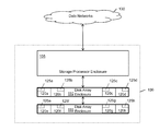
- FIG. 1 depicts storage system 100 , in accordance with the technology.
- Storage system 100 includes storage processor enclosure 105 .
- Storage processor enclosure 105 can include one or more storage processors (not shown).
- the storage processors can be any computing devices, such as servers, blade servers, etc.
- Storage system 100 includes disk array enclosure 110 and disk array enclosure 115 .
- Disk array enclosures 110 and 115 include drives 120 a - 120 h .
- Drives 120 a - 120 h can be any type of storage devices, such as magnetic disk drives, flash memory drives, solid state drives, etc.
- Drives 120 a - 120 h include drive controller modules 125 a - 125 h .
- storage processor enclosure 105 is connected to disk array enclosure 110 , which is connected to disk array enclosure 115 .
- the storage processors can read data from and write data to drives 120 a - 120 h .
- Drive controller modules 125 a - 125 h can control how data is written to and read from drives 120 a - 120 h .
- Storage system 100 can be connected to data networks 130 .
- the illustrated connections can each be any type of connection for communicating data.
- the storage processors in storage processor enclosure 105 service IO requests (e.g., commands to read data from or write data to storage system 100 ) received from data networks 130 .
- storage system 100 in FIG. 1 is an exemplary storage system in accordance with the technology.
- the storage processors and disk enclosures can be in the same enclosure.
- more or fewer disk array enclosures can be connected to the storage processors in the storage processor enclosure.
- the drive controller modules can be hardware.
- the drive controller modules can be software (e.g., software executing on the service processors) or firmware. Each drive controller module can control a single drive or multiple drives.
- FIGS. 2A-2C illustrate data written to drive 205 in accordance with the technology.
- drive 205 can be any of drives 120 a - 120 h shown in FIG. 1 .
- Drive 205 can store data blocks at addresses 210 a - 210 r .
- a data block can be any size.
- parity block P 1 can be stored on drive 205 at address 210 i .
- Parity block P 1 can be calculated based on data blocks A 1 -A 8 by, for example, a drive controller module associated with drive 205 .
- the data blocks e.g., data blocks A 1 -A 8
- Parity block P 1 can be calculated by performing an exclusive OR operation on data blocks A 1 -A 8 .
- the nth bit of parity block P 1 can be calculated by performing an exclusive OR operation on the nth bits from each of data blocks A 1 -A 8 .
- Other methods of error correction are contemplated.
- error correcting codes can be calculated across data blocks A 1 -A 8 and stored in place of parity block P 1 .
- the drive controller module can receive additional data blocks for writing to drive 205 .
- drive 205 is illustrated with data blocks A 1 -A 8 stored at addresses 210 a - 210 h and data blocks B 1 -B 8 stored at addresses 210 j - 210 q .
- parity block P 2 can be written to drive 205 at address 210 r . Parity block P 2 can be calculated, for example, by the drive controller module associated with drive 205 based on the data block parity group containing data blocks B 1 -B 8 .
- drive 205 is illustrated with data blocks A 1 -A 8 stored at addresses 210 a - 210 h , data blocks C 1 -C 4 stored at addressed 210 j - 210 m , and data blocks B 5 -B 8 stored at addresses 210 n - 210 q .
- data blocks C 1 -C 4 are written over data blocks B 1 -B 4 of FIG. 2B .
- parity block P 3 can be written to drive 205 at address 210 r . Parity block P 3 can be calculated, for example, by the drive controller module associated with drive 205 based on the data block parity group containing data blocks C 1 -C 4 and B 5 -B 8 .
- conventional techniques of providing atomicity can be used to ensure that all data blocks and the parity block are successfully written to the drive.
- the data block parity groups can be a fixed size.
- the data block parity group can be based on the data being stored. For example, a parity block can be written every, e.g., 4 or 8 blocks if the data is being written a few blocks at a time. If long sequential writes are common, a parity block can be written every, e.g., 100 or 200 blocks.
- the data block parity group can be variable sized.
- a header can be written to the drive to indicate the data blocks included in the data block parity group for a particular parity block. In some embodiments, the header can be written to another drive and/or stored in other memory on a storage system.
- the data blocks forming the data block parity group and the parity block are not stored consecutively and/or adjacently on the drive.
- a particular data block can be mapped to one or more sectors on the drive and, in the case of multiple sectors, the sectors can be non-consecutive. Accordingly, data of the data block parity group can be distributed on the drive.
- the parity block can be mapped to one or more sectors on the drive, and the sectors can be non-consecutive.
- the technology can facilitate data recovery after drive errors and/or failures. While magnetic disk drives can include ECC data to facilitate recovery from partial loss of a sector, in some cases the ECC data cannot be used to recover data when the entire sector is lost.
- the technology can facilitate recovering the data for a data block (e.g., the data for one or more failed sectors).
- the data stored on the failed sector can be recovered by performing an exclusive OR operation on the parity block and the remaining data blocks in the data block parity group. For example, with reference to FIG. 2C , one or more sector failures can cause data block A 1 stored at address 210 a to be unreadable.
- the value of data block A 1 can be recovered by performing an Exclusive OR operation on the data blocks A 2 -A 8 and parity block P 1 .
- the nth bit of data block A 1 can be calculated by performing an exclusive OR operation on the nth bits from each of data blocks A 2 -A 8 and parity block P 1 .
- the technology can facilitate recovery when multiple adjacent sectors fail.
- FIG. 3 depicts drive 305 and drive 310 , in accordance with the technology.
- Drive 305 and drive 310 are mirrored in a RAID 1 configuration. As illustrated, certain data written to drive 305 is also written to drive 310 .
- data blocks A 1 -A 4 are written to drive 305 at addresses 307 a - 307 d .
- a drive controller module associated with drive 305 calculates parity block P 1 , stored at address 307 e , based on the data block parity group containing data blocks A 1 -A 4 .
- Data blocks A 1 -A 4 are mirrored to drive 310 and stored at addresses 312 a - 312 d .
- a drive controller module associated with drive 310 calculates parity block P 1 , stored at address 312 e , based on the data block parity group containing data blocks A 1 -A 4 .
- Data blocks B 1 -B 4 are written to drive 305 at addresses 307 f - 307 i .
- a drive controller module associated with drive 305 calculates parity block P 2 , stored at address 307 j , based on the data block parity group containing data blocks B 1 -B 4 .
- Data blocks B 1 -B 4 are mirrored to drive 310 and stored at addresses 312 f - 312 i .
- a drive controller module associated with drive 310 calculates parity block P 2 , stored at address 312 j , based on the data block parity group containing data blocks B 1 -B 4 .
- a mirrored pair of drives in a conventional RAID 1 configuration can recover from one of the two drives failing. Data can be read from the remaining operational drive. However, in some instances the remaining operational drive cannot recover from additional errors on that drive, such as sector failures. Beneficially, the technology can improve error recovery. For example, if drive 305 fails, drive 310 can still recover from sector failures. If a sector failure makes address 312 a unreadable, data block A 1 can still be recovered using data blocks A 2 -A 4 (stored at addresses 312 b - 312 d ) and parity block P 1 (stored at address 312 e ), as described above.
- FIG. 4 depicts drive 405 , drive 410 , drive 415 , and drive 420 in accordance with the technology.
- Drives 405 , 410 , 415 , and 420 are in a RAID 5 configuration.
- data blocks A 1 -A 3 are striped across drives 405 , 410 , and 415 .
- Data block A 1 is stored at address 407 a of drive 405 .
- Data block A 2 is stored at address 412 a of drive 410 .
- Data block A 3 is stored at address 417 a of drive 415 .
- Data block A P (e.g., a parity block calculated based on data blocks A 1 -A 3 ) is stored at address 422 a of drive 420 .
- Data blocks B 1 -B 3 are striped across drives 405 , 410 , and 420 .
- Data block B 1 is stored at address 407 b of drive 405 .
- Data block B 2 is stored at address 412 b of drive 410 .
- Data block B 3 is stored at address 422 b of drive 420 .
- Data block B P (e.g., a parity block calculated based on data blocks B 1 -B 3 ) is stored at address 417 b of drive 415 .
- Data blocks C 1 -C 3 and data block C P , data blocks D 1 -D 3 and data block D P , data blocks E 1 -E 3 and data block E P , data blocks F 1 -F 3 and data block F P , data blocks G 1 -G 3 and data block G P , and data blocks H 1 -H 3 and data block H P are similarly striped across drives 405 , 410 , 415 , and 420 as illustrated.
- parity block P 1 stored at address 407 e of drive 405 , is calculated based on the data block parity group containing data blocks A 1 , B 1 , C 1 , and D P .
- Parity block P 2 stored at address 412 e of drive 410 , is calculated based on the data block parity group containing data blocks A 2 , B 2 , C P , and D 1 .
- Parity block P 3 stored at address 417 e of drive 415 , is calculated based on the data block parity group containing data blocks A 3 , B P , C 2 , and D 2 .
- Parity block P 4 stored at address 422 e of drive 420 , is calculated based on the data block parity group containing data blocks A P , B 3 , C 3 , and D 3 .
- Parity block P 5 stored at address 407 j of drive 405 , is calculated based on the data block parity group containing data blocks E 1 , F 1 , G 1 , and H P .
- Parity block P 6 stored at address 412 j of drive 410 , is calculated based on the data block parity group containing data blocks E 2 , F 2 , G P , and H 1 .
- Parity block P 7 stored at address 417 j of drive 415 , is calculated based on the data block parity group containing data blocks E 3 , F P , G 2 , and H 2 .
- Parity block P 8 stored at address 422 j of drive 420 , is calculated based on the data block parity group containing data blocks E P , F 3 , G 3 , and H 3 .
- the technology can facilitate recovery of data in some instances where a conventional RAID 5 configuration could not recover the data. For example, if drive 405 fails and a sector failure causes data block A 2 to be unreadable, the technology can facilitate recovery of data block A 1 and data block A 2 . As described above, data block A 2 can be recovered using data blocks B 2 , C P , D 1 , and P 2 . Data block A 1 can then be recovered using data blocks A 2 , A 3 , and A P . More generally, the technology can facilitate data recovery of similar drive and sector failures.
- FIG. 5 depicts a flowchart illustrating a method of enhancing error recovery for a data storage drive.
- a first one or more data blocks are received to write to a first drive.
- data blocks A 1 -A 8 can be received.
- a first parity block is calculated based on a first data block parity group.
- the data block parity group can contain the one or more data blocks.
- parity block P 1 can be calculated based on data blocks A 1 -A 8 .
- the one or more data blocks are written to the first drive. For example, as described above with reference to FIG.
- data blocks A 1 -A 8 are written to addresses 210 a - 210 h of drive 205 .
- the first parity block is written to the first drive.
- parity block P 1 is written to address 210 i of drive 205 . It should be appreciated that the steps of the described method can occur in other orders and/or in parallel. For example, steps 520 and 540 can be performed before, after, or in parallel with step 530 .
- FIG. 6 depicts a flowchart illustrating a method of recovering a data block on a drive.
- a first data block on a first drive is unreadable, where the first data block is a member of a first data block parity group.
- a first data block can be unreadable due to a sector failure on the first drive.
- a second one or more data blocks are read from the first drive, where the second one or more data blocks are from the first data block parity group.
- the remaining data blocks in the data block parity group associated with the unreadable data block can be read from the drive.
- a first parity block associated with the first data block parity group is read from the drive.
- the parity block associated with the unreadable block can be read from the drive.
- a value of the first data block is calculated based on the second one or more data blocks and the first parity block.
- the unreadable data block can be recovered based on the associated parity block and the remaining data blocks from the data block parity group associated with the unreadable data block.
- the above-described techniques can be implemented in digital electronic circuitry, or in computer hardware, firmware, software, or in combinations of them.
- the implementation can be as a computer program product, i.e., a computer program tangibly embodied in an information carrier, e.g., in a machine-readable storage device or in a propagated signal, for execution by, or to control the operation of, data processing apparatus, e.g., a programmable processor, a computer, or multiple computers.
- a computer program can be written in any form of programming language, including compiled or interpreted languages, and it can be deployed in any form, including as a stand-alone program or as a module, component, subroutine, or other unit suitable for use in a computing environment.
- a computer program can be deployed to be executed on one computer or on multiple computers at one site or distributed across multiple sites and interconnected by a communication network.
- processors suitable for the execution of a computer program include, by way of example, both general and special purpose microprocessors, and any one or more processors of any kind of digital computer.
- a processor receives instructions and data from a read-only memory or a random access memory or both.
- the essential elements of a computer are a processor for executing instructions and one or more memory devices for storing instructions and data.
- a computer also includes, or be operatively coupled to receive data from or transfer data to, or both, one or more mass storage devices or drives for storing data, e.g., magnetic, magneto-optical disks, or optical disks. Data transmission and instructions can also occur over a communications network.
- Information carriers suitable for embodying computer program instructions and data include all forms of non-volatile memory, including by way of example semiconductor memory devices, e.g., EPROM, EEPROM, and flash memory devices; magnetic disks, e.g., internal hard disks or removable disks; magneto-optical disks; and CD-ROM and DVD-ROM disks.
- semiconductor memory devices e.g., EPROM, EEPROM, and flash memory devices
- magnetic disks e.g., internal hard disks or removable disks
- magneto-optical disks e.g., CD-ROM and DVD-ROM disks.
- the processor and the memory can be supplemented by, or incorporated in special purpose logic circuitry.
- the above described techniques can be implemented on a computer having a display device, e.g., a CRT (cathode ray tube) or LCD (liquid crystal display) monitor, for displaying information to the user and a keyboard and a pointing device, e.g., a mouse or a trackball, by which the user can provide input to the computer (e.g., interact with a user interface element).
- a display device e.g., a CRT (cathode ray tube) or LCD (liquid crystal display) monitor
- a keyboard and a pointing device e.g., a mouse or a trackball
- Other kinds of devices can be used to provide for interaction with a user as well; for example, feedback provided to the user can be any form of sensory feedback, e.g., visual feedback, auditory feedback, or tactile feedback; and input from the user can be received in any form, including acoustic, speech, or tactile input.
- the above described techniques can be implemented in a distributed computing system that includes a back-end component, e.g., as a data server, and/or a middleware component, e.g., an application server, and/or a front-end component, e.g., a client computer having a graphical user interface and/or a Web browser through which a user can interact with an example implementation, or any combination of such back-end, middleware, or front-end components.
- the components of the system can be interconnected by any form or medium of digital data communication, e.g., a communication network. Examples of communication networks include a local area network (“LAN”) and a wide area network (“WAN”), e.g., the Internet, and include both wired and wireless networks.
- LAN local area network
- WAN wide area network
- the computing system can include clients and servers.
- a client and server are generally remote from each other and typically interact through a communication network.
- the relationship of client and server arises by virtue of computer programs running on the respective computers and having a client-server relationship to each other.
Landscapes
- Engineering & Computer Science (AREA)
- Theoretical Computer Science (AREA)
- Physics & Mathematics (AREA)
- General Engineering & Computer Science (AREA)
- General Physics & Mathematics (AREA)
- Quality & Reliability (AREA)
- Human Computer Interaction (AREA)
- Computer Security & Cryptography (AREA)
- Techniques For Improving Reliability Of Storages (AREA)
Abstract
Description
Claims (12)
Priority Applications (1)
| Application Number | Priority Date | Filing Date | Title |
|---|---|---|---|
| US14/500,471 US9830220B1 (en) | 2014-09-29 | 2014-09-29 | Enhanced error recovery for data storage drives |
Applications Claiming Priority (1)
| Application Number | Priority Date | Filing Date | Title |
|---|---|---|---|
| US14/500,471 US9830220B1 (en) | 2014-09-29 | 2014-09-29 | Enhanced error recovery for data storage drives |
Publications (1)
| Publication Number | Publication Date |
|---|---|
| US9830220B1 true US9830220B1 (en) | 2017-11-28 |
Family
ID=60408594
Family Applications (1)
| Application Number | Title | Priority Date | Filing Date |
|---|---|---|---|
| US14/500,471 Active 2035-03-08 US9830220B1 (en) | 2014-09-29 | 2014-09-29 | Enhanced error recovery for data storage drives |
Country Status (1)
| Country | Link |
|---|---|
| US (1) | US9830220B1 (en) |
Cited By (1)
| Publication number | Priority date | Publication date | Assignee | Title |
|---|---|---|---|---|
| TWI656442B (en) * | 2017-11-30 | 2019-04-11 | 慧榮科技股份有限公司 | Method for access control in a memory device, and memory device and controller thereof |
Citations (26)
| Publication number | Priority date | Publication date | Assignee | Title |
|---|---|---|---|---|
| US5504858A (en) * | 1993-06-29 | 1996-04-02 | Digital Equipment Corporation | Method and apparatus for preserving data integrity in a multiple disk raid organized storage system |
| US5522032A (en) * | 1994-05-05 | 1996-05-28 | International Business Machines Corporation | Raid level 5 with free blocks parity cache |
| US5745671A (en) * | 1995-02-28 | 1998-04-28 | International Business Machines Corporation | Data storage system with localized XOR function |
| US5748885A (en) * | 1994-12-23 | 1998-05-05 | Emc Corporation | Method and apparatus for reduction of I/O operations in persistent storage system |
| US20020161972A1 (en) * | 2001-04-30 | 2002-10-31 | Talagala Nisha D. | Data storage array employing block checksums and dynamic striping |
| US6480970B1 (en) * | 2000-05-17 | 2002-11-12 | Lsi Logic Corporation | Method of verifying data consistency between local and remote mirrored data storage systems |
| US20020178325A1 (en) * | 2001-05-25 | 2002-11-28 | Allingham Donald N. | Method and apparatus for scalable error correction code generation performance |
| US20030120674A1 (en) * | 2001-12-25 | 2003-06-26 | Hitachi, Ltd. | Control method of control device conducting data input and output to storage devices, and control device used therefor |
| US20030188097A1 (en) * | 2002-03-29 | 2003-10-02 | Holland Mark C. | Data file migration from a mirrored RAID to a non-mirrored XOR-based RAID without rewriting the data |
| US6675318B1 (en) * | 2000-07-25 | 2004-01-06 | Sun Microsystems, Inc. | Two-dimensional storage array with prompt parity in one dimension and delayed parity in a second dimension |
| US6799283B1 (en) * | 1998-12-04 | 2004-09-28 | Matsushita Electric Industrial Co., Ltd. | Disk array device |
| US20050283654A1 (en) * | 2004-05-24 | 2005-12-22 | Sun Microsystems, Inc. | Method and apparatus for decreasing failed disk reconstruction time in a raid data storage system |
| US20060080505A1 (en) * | 2004-10-08 | 2006-04-13 | Masahiro Arai | Disk array device and control method for same |
| US20060101202A1 (en) * | 2004-11-11 | 2006-05-11 | Akihiro Mannen | Disk array system |
| US20070028045A1 (en) * | 2005-08-01 | 2007-02-01 | Infortrend Technology Inc. | Method for improving writing data efficiency and storage subsystem and system implementing the same |
| US7337287B2 (en) * | 2004-01-28 | 2008-02-26 | Hitachi, Ltd. | Storage unit, storage unit control method, and storage system |
| US20090259882A1 (en) * | 2008-04-15 | 2009-10-15 | Dot Hill Systems Corporation | Apparatus and method for identifying disk drives with unreported data corruption |
| US8037244B2 (en) * | 2007-10-19 | 2011-10-11 | Hitachi, Ltd. | Storage apparatus and data storage method using the same |
| US8209587B1 (en) * | 2007-04-12 | 2012-06-26 | Netapp, Inc. | System and method for eliminating zeroing of disk drives in RAID arrays |
| US8239706B1 (en) * | 2007-01-03 | 2012-08-07 | Board Of Governors For Higher Education, State Of Rhode Island And Providence Plantations | Data retrieval system and method that provides retrieval of data to any point in time |
| US20130067273A1 (en) * | 2011-09-12 | 2013-03-14 | International Business Machines Corporation | Optimizing and Enhancing Performance for Parity Based Storage |
| US8527698B2 (en) * | 2010-06-22 | 2013-09-03 | Lsi Corporation | Parity-based raid system configured to protect against data corruption caused by the occurrence of write holes |
| US8862818B1 (en) * | 2012-09-27 | 2014-10-14 | Emc Corporation | Handling partial stripe writes in log-structured storage |
| US8898381B2 (en) * | 2009-12-08 | 2014-11-25 | OCZ Storage Solutions Inc. | Raid storage systems having arrays of solid-state drives and methods of operation |
| US20160018995A1 (en) * | 2014-07-17 | 2016-01-21 | Lsi Corporation | Raid system for processing i/o requests utilizing xor commands |
| US20160034186A1 (en) * | 2014-07-30 | 2016-02-04 | Lsi Corporation | Host-based device drivers for enhancing operations in redundant array of independent disks systems |
-
2014
- 2014-09-29 US US14/500,471 patent/US9830220B1/en active Active
Patent Citations (26)
| Publication number | Priority date | Publication date | Assignee | Title |
|---|---|---|---|---|
| US5504858A (en) * | 1993-06-29 | 1996-04-02 | Digital Equipment Corporation | Method and apparatus for preserving data integrity in a multiple disk raid organized storage system |
| US5522032A (en) * | 1994-05-05 | 1996-05-28 | International Business Machines Corporation | Raid level 5 with free blocks parity cache |
| US5748885A (en) * | 1994-12-23 | 1998-05-05 | Emc Corporation | Method and apparatus for reduction of I/O operations in persistent storage system |
| US5745671A (en) * | 1995-02-28 | 1998-04-28 | International Business Machines Corporation | Data storage system with localized XOR function |
| US6799283B1 (en) * | 1998-12-04 | 2004-09-28 | Matsushita Electric Industrial Co., Ltd. | Disk array device |
| US6480970B1 (en) * | 2000-05-17 | 2002-11-12 | Lsi Logic Corporation | Method of verifying data consistency between local and remote mirrored data storage systems |
| US6675318B1 (en) * | 2000-07-25 | 2004-01-06 | Sun Microsystems, Inc. | Two-dimensional storage array with prompt parity in one dimension and delayed parity in a second dimension |
| US20020161972A1 (en) * | 2001-04-30 | 2002-10-31 | Talagala Nisha D. | Data storage array employing block checksums and dynamic striping |
| US20020178325A1 (en) * | 2001-05-25 | 2002-11-28 | Allingham Donald N. | Method and apparatus for scalable error correction code generation performance |
| US20030120674A1 (en) * | 2001-12-25 | 2003-06-26 | Hitachi, Ltd. | Control method of control device conducting data input and output to storage devices, and control device used therefor |
| US20030188097A1 (en) * | 2002-03-29 | 2003-10-02 | Holland Mark C. | Data file migration from a mirrored RAID to a non-mirrored XOR-based RAID without rewriting the data |
| US7337287B2 (en) * | 2004-01-28 | 2008-02-26 | Hitachi, Ltd. | Storage unit, storage unit control method, and storage system |
| US20050283654A1 (en) * | 2004-05-24 | 2005-12-22 | Sun Microsystems, Inc. | Method and apparatus for decreasing failed disk reconstruction time in a raid data storage system |
| US20060080505A1 (en) * | 2004-10-08 | 2006-04-13 | Masahiro Arai | Disk array device and control method for same |
| US20060101202A1 (en) * | 2004-11-11 | 2006-05-11 | Akihiro Mannen | Disk array system |
| US20070028045A1 (en) * | 2005-08-01 | 2007-02-01 | Infortrend Technology Inc. | Method for improving writing data efficiency and storage subsystem and system implementing the same |
| US8239706B1 (en) * | 2007-01-03 | 2012-08-07 | Board Of Governors For Higher Education, State Of Rhode Island And Providence Plantations | Data retrieval system and method that provides retrieval of data to any point in time |
| US8209587B1 (en) * | 2007-04-12 | 2012-06-26 | Netapp, Inc. | System and method for eliminating zeroing of disk drives in RAID arrays |
| US8037244B2 (en) * | 2007-10-19 | 2011-10-11 | Hitachi, Ltd. | Storage apparatus and data storage method using the same |
| US20090259882A1 (en) * | 2008-04-15 | 2009-10-15 | Dot Hill Systems Corporation | Apparatus and method for identifying disk drives with unreported data corruption |
| US8898381B2 (en) * | 2009-12-08 | 2014-11-25 | OCZ Storage Solutions Inc. | Raid storage systems having arrays of solid-state drives and methods of operation |
| US8527698B2 (en) * | 2010-06-22 | 2013-09-03 | Lsi Corporation | Parity-based raid system configured to protect against data corruption caused by the occurrence of write holes |
| US20130067273A1 (en) * | 2011-09-12 | 2013-03-14 | International Business Machines Corporation | Optimizing and Enhancing Performance for Parity Based Storage |
| US8862818B1 (en) * | 2012-09-27 | 2014-10-14 | Emc Corporation | Handling partial stripe writes in log-structured storage |
| US20160018995A1 (en) * | 2014-07-17 | 2016-01-21 | Lsi Corporation | Raid system for processing i/o requests utilizing xor commands |
| US20160034186A1 (en) * | 2014-07-30 | 2016-02-04 | Lsi Corporation | Host-based device drivers for enhancing operations in redundant array of independent disks systems |
Cited By (3)
| Publication number | Priority date | Publication date | Assignee | Title |
|---|---|---|---|---|
| TWI656442B (en) * | 2017-11-30 | 2019-04-11 | 慧榮科技股份有限公司 | Method for access control in a memory device, and memory device and controller thereof |
| US10705749B2 (en) | 2017-11-30 | 2020-07-07 | Silicon Motion, Inc. | Method for performing access control in a memory device, associated memory device and controller thereof |
| US11294589B2 (en) | 2017-11-30 | 2022-04-05 | Silicon Motion, Inc. | Method for performing access control in a memory device, associated memory device and controller thereof |
Similar Documents
| Publication | Publication Date | Title |
|---|---|---|
| US11784667B2 (en) | Selecting optimal responses to errors in a storage system | |
| US10191676B2 (en) | Scalable storage protection | |
| US8856619B1 (en) | Storing data across groups of storage nodes | |
| US20190171524A1 (en) | Isolating the introduction of software defects in a dispersed storage network | |
| US9690657B2 (en) | Writing data across storage devices in an erasure-coded system | |
| US10572345B2 (en) | First responder parities for storage array | |
| US7827439B2 (en) | System and method of redundantly storing and retrieving data with cooperating storage devices | |
| US8930750B2 (en) | Systems and methods for preventing data loss | |
| US8010875B2 (en) | Error correcting code with chip kill capability and power saving enhancement | |
| US7689890B2 (en) | System and method for handling write commands to prevent corrupted parity information in a storage array | |
| US10394651B2 (en) | Computing system with circular-shift recovery mechanism and method of operation thereof | |
| US20130198585A1 (en) | Method of, and apparatus for, improved data integrity | |
| US9753807B1 (en) | Generation and verification of erasure encoded fragments | |
| US9489254B1 (en) | Verification of erasure encoded fragments | |
| US11314594B2 (en) | Method, device and computer program product for recovering data | |
| US8484536B1 (en) | Techniques for data storage, access, and maintenance | |
| US9552254B1 (en) | Verification of erasure encoded fragments | |
| US8621317B1 (en) | Modified orthogonal coding techniques for storing data | |
| JP2005004753A (en) | Method and device of performing data version checking | |
| US7577804B2 (en) | Detecting data integrity | |
| US11275513B2 (en) | System and method for selecting a redundant array of independent disks (RAID) level for a storage device segment extent | |
| US9830220B1 (en) | Enhanced error recovery for data storage drives | |
| US20170228166A1 (en) | Protecting in-memory immutable objects through hybrid hardware/software-based memory fault tolerance | |
| US10409772B2 (en) | Accessing serially stored data in a dispersed storage network | |
| US10733052B2 (en) | Accelerated rebuilding of storage arrays |
Legal Events
| Date | Code | Title | Description |
|---|---|---|---|
| AS | Assignment |
Owner name: EMC CORPORATION, MASSACHUSETTS Free format text: ASSIGNMENT OF ASSIGNORS INTEREST;ASSIGNOR:HARVEY, DAVID W.;REEL/FRAME:033870/0312 Effective date: 20140930 |
|
| AS | Assignment |
Owner name: CREDIT SUISSE AG, CAYMAN ISLANDS BRANCH, AS COLLATERAL AGENT, NORTH CAROLINA Free format text: SECURITY AGREEMENT;ASSIGNORS:ASAP SOFTWARE EXPRESS, INC.;AVENTAIL LLC;CREDANT TECHNOLOGIES, INC.;AND OTHERS;REEL/FRAME:040134/0001 Effective date: 20160907 Owner name: THE BANK OF NEW YORK MELLON TRUST COMPANY, N.A., AS NOTES COLLATERAL AGENT, TEXAS Free format text: SECURITY AGREEMENT;ASSIGNORS:ASAP SOFTWARE EXPRESS, INC.;AVENTAIL LLC;CREDANT TECHNOLOGIES, INC.;AND OTHERS;REEL/FRAME:040136/0001 Effective date: 20160907 Owner name: THE BANK OF NEW YORK MELLON TRUST COMPANY, N.A., A Free format text: SECURITY AGREEMENT;ASSIGNORS:ASAP SOFTWARE EXPRESS, INC.;AVENTAIL LLC;CREDANT TECHNOLOGIES, INC.;AND OTHERS;REEL/FRAME:040136/0001 Effective date: 20160907 Owner name: CREDIT SUISSE AG, CAYMAN ISLANDS BRANCH, AS COLLAT Free format text: SECURITY AGREEMENT;ASSIGNORS:ASAP SOFTWARE EXPRESS, INC.;AVENTAIL LLC;CREDANT TECHNOLOGIES, INC.;AND OTHERS;REEL/FRAME:040134/0001 Effective date: 20160907 |
|
| AS | Assignment |
Owner name: EMC IP HOLDING COMPANY LLC, MASSACHUSETTS Free format text: ASSIGNMENT OF ASSIGNORS INTEREST;ASSIGNOR:EMC CORPORATION;REEL/FRAME:040203/0001 Effective date: 20160906 |
|
| STCF | Information on status: patent grant |
Free format text: PATENTED CASE |
|
| AS | Assignment |
Owner name: THE BANK OF NEW YORK MELLON TRUST COMPANY, N.A., T Free format text: SECURITY AGREEMENT;ASSIGNORS:CREDANT TECHNOLOGIES, INC.;DELL INTERNATIONAL L.L.C.;DELL MARKETING L.P.;AND OTHERS;REEL/FRAME:049452/0223 Effective date: 20190320 Owner name: THE BANK OF NEW YORK MELLON TRUST COMPANY, N.A., TEXAS Free format text: SECURITY AGREEMENT;ASSIGNORS:CREDANT TECHNOLOGIES, INC.;DELL INTERNATIONAL L.L.C.;DELL MARKETING L.P.;AND OTHERS;REEL/FRAME:049452/0223 Effective date: 20190320 |
|
| AS | Assignment |
Owner name: THE BANK OF NEW YORK MELLON TRUST COMPANY, N.A., TEXAS Free format text: SECURITY AGREEMENT;ASSIGNORS:CREDANT TECHNOLOGIES INC.;DELL INTERNATIONAL L.L.C.;DELL MARKETING L.P.;AND OTHERS;REEL/FRAME:053546/0001 Effective date: 20200409 |
|
| MAFP | Maintenance fee payment |
Free format text: PAYMENT OF MAINTENANCE FEE, 4TH YEAR, LARGE ENTITY (ORIGINAL EVENT CODE: M1551); ENTITY STATUS OF PATENT OWNER: LARGE ENTITY Year of fee payment: 4 |
|
| AS | Assignment |
Owner name: WYSE TECHNOLOGY L.L.C., CALIFORNIA Free format text: RELEASE BY SECURED PARTY;ASSIGNOR:CREDIT SUISSE AG, CAYMAN ISLANDS BRANCH;REEL/FRAME:058216/0001 Effective date: 20211101 Owner name: SCALEIO LLC, MASSACHUSETTS Free format text: RELEASE BY SECURED PARTY;ASSIGNOR:CREDIT SUISSE AG, CAYMAN ISLANDS BRANCH;REEL/FRAME:058216/0001 Effective date: 20211101 Owner name: MOZY, INC., WASHINGTON Free format text: RELEASE BY SECURED PARTY;ASSIGNOR:CREDIT SUISSE AG, CAYMAN ISLANDS BRANCH;REEL/FRAME:058216/0001 Effective date: 20211101 Owner name: MAGINATICS LLC, CALIFORNIA Free format text: RELEASE BY SECURED PARTY;ASSIGNOR:CREDIT SUISSE AG, CAYMAN ISLANDS BRANCH;REEL/FRAME:058216/0001 Effective date: 20211101 Owner name: FORCE10 NETWORKS, INC., CALIFORNIA Free format text: RELEASE BY SECURED PARTY;ASSIGNOR:CREDIT SUISSE AG, CAYMAN ISLANDS BRANCH;REEL/FRAME:058216/0001 Effective date: 20211101 Owner name: EMC IP HOLDING COMPANY LLC, TEXAS Free format text: RELEASE BY SECURED PARTY;ASSIGNOR:CREDIT SUISSE AG, CAYMAN ISLANDS BRANCH;REEL/FRAME:058216/0001 Effective date: 20211101 Owner name: EMC CORPORATION, MASSACHUSETTS Free format text: RELEASE BY SECURED PARTY;ASSIGNOR:CREDIT SUISSE AG, CAYMAN ISLANDS BRANCH;REEL/FRAME:058216/0001 Effective date: 20211101 Owner name: DELL SYSTEMS CORPORATION, TEXAS Free format text: RELEASE BY SECURED PARTY;ASSIGNOR:CREDIT SUISSE AG, CAYMAN ISLANDS BRANCH;REEL/FRAME:058216/0001 Effective date: 20211101 Owner name: DELL SOFTWARE INC., CALIFORNIA Free format text: RELEASE BY SECURED PARTY;ASSIGNOR:CREDIT SUISSE AG, CAYMAN ISLANDS BRANCH;REEL/FRAME:058216/0001 Effective date: 20211101 Owner name: DELL PRODUCTS L.P., TEXAS Free format text: RELEASE BY SECURED PARTY;ASSIGNOR:CREDIT SUISSE AG, CAYMAN ISLANDS BRANCH;REEL/FRAME:058216/0001 Effective date: 20211101 Owner name: DELL MARKETING L.P., TEXAS Free format text: RELEASE BY SECURED PARTY;ASSIGNOR:CREDIT SUISSE AG, CAYMAN ISLANDS BRANCH;REEL/FRAME:058216/0001 Effective date: 20211101 Owner name: DELL INTERNATIONAL, L.L.C., TEXAS Free format text: RELEASE BY SECURED PARTY;ASSIGNOR:CREDIT SUISSE AG, CAYMAN ISLANDS BRANCH;REEL/FRAME:058216/0001 Effective date: 20211101 Owner name: DELL USA L.P., TEXAS Free format text: RELEASE BY SECURED PARTY;ASSIGNOR:CREDIT SUISSE AG, CAYMAN ISLANDS BRANCH;REEL/FRAME:058216/0001 Effective date: 20211101 Owner name: CREDANT TECHNOLOGIES, INC., TEXAS Free format text: RELEASE BY SECURED PARTY;ASSIGNOR:CREDIT SUISSE AG, CAYMAN ISLANDS BRANCH;REEL/FRAME:058216/0001 Effective date: 20211101 Owner name: AVENTAIL LLC, CALIFORNIA Free format text: RELEASE BY SECURED PARTY;ASSIGNOR:CREDIT SUISSE AG, CAYMAN ISLANDS BRANCH;REEL/FRAME:058216/0001 Effective date: 20211101 Owner name: ASAP SOFTWARE EXPRESS, INC., ILLINOIS Free format text: RELEASE BY SECURED PARTY;ASSIGNOR:CREDIT SUISSE AG, CAYMAN ISLANDS BRANCH;REEL/FRAME:058216/0001 Effective date: 20211101 |
|
| AS | Assignment |
Owner name: SCALEIO LLC, MASSACHUSETTS Free format text: RELEASE OF SECURITY INTEREST IN PATENTS PREVIOUSLY RECORDED AT REEL/FRAME (040136/0001);ASSIGNOR:THE BANK OF NEW YORK MELLON TRUST COMPANY, N.A., AS NOTES COLLATERAL AGENT;REEL/FRAME:061324/0001 Effective date: 20220329 Owner name: EMC IP HOLDING COMPANY LLC (ON BEHALF OF ITSELF AND AS SUCCESSOR-IN-INTEREST TO MOZY, INC.), TEXAS Free format text: RELEASE OF SECURITY INTEREST IN PATENTS PREVIOUSLY RECORDED AT REEL/FRAME (040136/0001);ASSIGNOR:THE BANK OF NEW YORK MELLON TRUST COMPANY, N.A., AS NOTES COLLATERAL AGENT;REEL/FRAME:061324/0001 Effective date: 20220329 Owner name: EMC CORPORATION (ON BEHALF OF ITSELF AND AS SUCCESSOR-IN-INTEREST TO MAGINATICS LLC), MASSACHUSETTS Free format text: RELEASE OF SECURITY INTEREST IN PATENTS PREVIOUSLY RECORDED AT REEL/FRAME (040136/0001);ASSIGNOR:THE BANK OF NEW YORK MELLON TRUST COMPANY, N.A., AS NOTES COLLATERAL AGENT;REEL/FRAME:061324/0001 Effective date: 20220329 Owner name: DELL MARKETING CORPORATION (SUCCESSOR-IN-INTEREST TO FORCE10 NETWORKS, INC. AND WYSE TECHNOLOGY L.L.C.), TEXAS Free format text: RELEASE OF SECURITY INTEREST IN PATENTS PREVIOUSLY RECORDED AT REEL/FRAME (040136/0001);ASSIGNOR:THE BANK OF NEW YORK MELLON TRUST COMPANY, N.A., AS NOTES COLLATERAL AGENT;REEL/FRAME:061324/0001 Effective date: 20220329 Owner name: DELL PRODUCTS L.P., TEXAS Free format text: RELEASE OF SECURITY INTEREST IN PATENTS PREVIOUSLY RECORDED AT REEL/FRAME (040136/0001);ASSIGNOR:THE BANK OF NEW YORK MELLON TRUST COMPANY, N.A., AS NOTES COLLATERAL AGENT;REEL/FRAME:061324/0001 Effective date: 20220329 Owner name: DELL INTERNATIONAL L.L.C., TEXAS Free format text: RELEASE OF SECURITY INTEREST IN PATENTS PREVIOUSLY RECORDED AT REEL/FRAME (040136/0001);ASSIGNOR:THE BANK OF NEW YORK MELLON TRUST COMPANY, N.A., AS NOTES COLLATERAL AGENT;REEL/FRAME:061324/0001 Effective date: 20220329 Owner name: DELL USA L.P., TEXAS Free format text: RELEASE OF SECURITY INTEREST IN PATENTS PREVIOUSLY RECORDED AT REEL/FRAME (040136/0001);ASSIGNOR:THE BANK OF NEW YORK MELLON TRUST COMPANY, N.A., AS NOTES COLLATERAL AGENT;REEL/FRAME:061324/0001 Effective date: 20220329 Owner name: DELL MARKETING L.P. (ON BEHALF OF ITSELF AND AS SUCCESSOR-IN-INTEREST TO CREDANT TECHNOLOGIES, INC.), TEXAS Free format text: RELEASE OF SECURITY INTEREST IN PATENTS PREVIOUSLY RECORDED AT REEL/FRAME (040136/0001);ASSIGNOR:THE BANK OF NEW YORK MELLON TRUST COMPANY, N.A., AS NOTES COLLATERAL AGENT;REEL/FRAME:061324/0001 Effective date: 20220329 Owner name: DELL MARKETING CORPORATION (SUCCESSOR-IN-INTEREST TO ASAP SOFTWARE EXPRESS, INC.), TEXAS Free format text: RELEASE OF SECURITY INTEREST IN PATENTS PREVIOUSLY RECORDED AT REEL/FRAME (040136/0001);ASSIGNOR:THE BANK OF NEW YORK MELLON TRUST COMPANY, N.A., AS NOTES COLLATERAL AGENT;REEL/FRAME:061324/0001 Effective date: 20220329 |
|
| AS | Assignment |
Owner name: SCALEIO LLC, MASSACHUSETTS Free format text: RELEASE OF SECURITY INTEREST IN PATENTS PREVIOUSLY RECORDED AT REEL/FRAME (045455/0001);ASSIGNOR:THE BANK OF NEW YORK MELLON TRUST COMPANY, N.A., AS NOTES COLLATERAL AGENT;REEL/FRAME:061753/0001 Effective date: 20220329 Owner name: EMC IP HOLDING COMPANY LLC (ON BEHALF OF ITSELF AND AS SUCCESSOR-IN-INTEREST TO MOZY, INC.), TEXAS Free format text: RELEASE OF SECURITY INTEREST IN PATENTS PREVIOUSLY RECORDED AT REEL/FRAME (045455/0001);ASSIGNOR:THE BANK OF NEW YORK MELLON TRUST COMPANY, N.A., AS NOTES COLLATERAL AGENT;REEL/FRAME:061753/0001 Effective date: 20220329 Owner name: EMC CORPORATION (ON BEHALF OF ITSELF AND AS SUCCESSOR-IN-INTEREST TO MAGINATICS LLC), MASSACHUSETTS Free format text: RELEASE OF SECURITY INTEREST IN PATENTS PREVIOUSLY RECORDED AT REEL/FRAME (045455/0001);ASSIGNOR:THE BANK OF NEW YORK MELLON TRUST COMPANY, N.A., AS NOTES COLLATERAL AGENT;REEL/FRAME:061753/0001 Effective date: 20220329 Owner name: DELL MARKETING CORPORATION (SUCCESSOR-IN-INTEREST TO FORCE10 NETWORKS, INC. AND WYSE TECHNOLOGY L.L.C.), TEXAS Free format text: RELEASE OF SECURITY INTEREST IN PATENTS PREVIOUSLY RECORDED AT REEL/FRAME (045455/0001);ASSIGNOR:THE BANK OF NEW YORK MELLON TRUST COMPANY, N.A., AS NOTES COLLATERAL AGENT;REEL/FRAME:061753/0001 Effective date: 20220329 Owner name: DELL PRODUCTS L.P., TEXAS Free format text: RELEASE OF SECURITY INTEREST IN PATENTS PREVIOUSLY RECORDED AT REEL/FRAME (045455/0001);ASSIGNOR:THE BANK OF NEW YORK MELLON TRUST COMPANY, N.A., AS NOTES COLLATERAL AGENT;REEL/FRAME:061753/0001 Effective date: 20220329 Owner name: DELL INTERNATIONAL L.L.C., TEXAS Free format text: RELEASE OF SECURITY INTEREST IN PATENTS PREVIOUSLY RECORDED AT REEL/FRAME (045455/0001);ASSIGNOR:THE BANK OF NEW YORK MELLON TRUST COMPANY, N.A., AS NOTES COLLATERAL AGENT;REEL/FRAME:061753/0001 Effective date: 20220329 Owner name: DELL USA L.P., TEXAS Free format text: RELEASE OF SECURITY INTEREST IN PATENTS PREVIOUSLY RECORDED AT REEL/FRAME (045455/0001);ASSIGNOR:THE BANK OF NEW YORK MELLON TRUST COMPANY, N.A., AS NOTES COLLATERAL AGENT;REEL/FRAME:061753/0001 Effective date: 20220329 Owner name: DELL MARKETING L.P. (ON BEHALF OF ITSELF AND AS SUCCESSOR-IN-INTEREST TO CREDANT TECHNOLOGIES, INC.), TEXAS Free format text: RELEASE OF SECURITY INTEREST IN PATENTS PREVIOUSLY RECORDED AT REEL/FRAME (045455/0001);ASSIGNOR:THE BANK OF NEW YORK MELLON TRUST COMPANY, N.A., AS NOTES COLLATERAL AGENT;REEL/FRAME:061753/0001 Effective date: 20220329 Owner name: DELL MARKETING CORPORATION (SUCCESSOR-IN-INTEREST TO ASAP SOFTWARE EXPRESS, INC.), TEXAS Free format text: RELEASE OF SECURITY INTEREST IN PATENTS PREVIOUSLY RECORDED AT REEL/FRAME (045455/0001);ASSIGNOR:THE BANK OF NEW YORK MELLON TRUST COMPANY, N.A., AS NOTES COLLATERAL AGENT;REEL/FRAME:061753/0001 Effective date: 20220329 |