US9825233B2 - Heterocyclic compound and organic light-emitting device including the same - Google Patents
Heterocyclic compound and organic light-emitting device including the same Download PDFInfo
- Publication number
- US9825233B2 US9825233B2 US14/012,545 US201314012545A US9825233B2 US 9825233 B2 US9825233 B2 US 9825233B2 US 201314012545 A US201314012545 A US 201314012545A US 9825233 B2 US9825233 B2 US 9825233B2
- Authority
- US
- United States
- Prior art keywords
- group
- layer
- organic light
- emitting device
- compound
- Prior art date
- Legal status (The legal status is an assumption and is not a legal conclusion. Google has not performed a legal analysis and makes no representation as to the accuracy of the status listed.)
- Active, expires
Links
- 150000002391 heterocyclic compounds Chemical class 0.000 title claims abstract description 22
- 239000010410 layer Substances 0.000 claims description 88
- 150000001875 compounds Chemical class 0.000 claims description 60
- 239000000463 material Substances 0.000 claims description 55
- 238000002347 injection Methods 0.000 claims description 37
- 239000007924 injection Substances 0.000 claims description 37
- 239000002346 layers by function Substances 0.000 claims description 27
- 239000002019 doping agent Substances 0.000 claims description 24
- 239000012044 organic layer Substances 0.000 claims description 23
- 230000005525 hole transport Effects 0.000 claims description 21
- 125000004093 cyano group Chemical group *C#N 0.000 claims description 13
- MWPLVEDNUUSJAV-UHFFFAOYSA-N anthracene Chemical compound C1=CC=CC2=CC3=CC=CC=C3C=C21 MWPLVEDNUUSJAV-UHFFFAOYSA-N 0.000 claims description 10
- 239000010409 thin film Substances 0.000 claims description 6
- 150000004696 coordination complex Chemical class 0.000 claims description 5
- 229910044991 metal oxide Inorganic materials 0.000 claims description 4
- 150000004706 metal oxides Chemical class 0.000 claims description 4
- 238000000034 method Methods 0.000 claims description 3
- 150000004982 aromatic amines Chemical class 0.000 claims description 2
- 150000004059 quinone derivatives Chemical class 0.000 claims description 2
- 125000005504 styryl group Chemical group 0.000 claims description 2
- 125000004435 hydrogen atom Chemical group [H]* 0.000 abstract description 17
- 125000003118 aryl group Chemical group 0.000 abstract description 16
- 125000003367 polycyclic group Chemical group 0.000 abstract description 15
- 229910052805 deuterium Inorganic materials 0.000 abstract description 13
- 125000004431 deuterium atom Chemical group 0.000 abstract description 13
- 125000000217 alkyl group Chemical group 0.000 abstract description 11
- 125000001072 heteroaryl group Chemical group 0.000 abstract description 10
- 230000015572 biosynthetic process Effects 0.000 description 35
- 238000003786 synthesis reaction Methods 0.000 description 30
- -1 isopropyloxy group Chemical group 0.000 description 26
- 150000003839 salts Chemical class 0.000 description 21
- 238000000151 deposition Methods 0.000 description 18
- 230000008021 deposition Effects 0.000 description 16
- 239000011248 coating agent Substances 0.000 description 15
- 238000000576 coating method Methods 0.000 description 15
- 229940125904 compound 1 Drugs 0.000 description 15
- 125000001424 substituent group Chemical group 0.000 description 14
- OAKJQQAXSVQMHS-UHFFFAOYSA-N Hydrazine Chemical compound NN OAKJQQAXSVQMHS-UHFFFAOYSA-N 0.000 description 13
- 239000000243 solution Substances 0.000 description 13
- 238000001771 vacuum deposition Methods 0.000 description 13
- YXFVVABEGXRONW-UHFFFAOYSA-N Toluene Chemical compound CC1=CC=CC=C1 YXFVVABEGXRONW-UHFFFAOYSA-N 0.000 description 12
- 238000000921 elemental analysis Methods 0.000 description 12
- 125000001997 phenyl group Chemical group [H]C1=C([H])C([H])=C(*)C([H])=C1[H] 0.000 description 12
- 239000000758 substrate Substances 0.000 description 12
- 125000001624 naphthyl group Chemical group 0.000 description 11
- 238000004528 spin coating Methods 0.000 description 11
- 0 CCC.CC[Ar].[1*]C1=C([2*])C([3*])=C([4*])C2=C1C1=C(C=BC=*1)C1=C2[2H]=CC=C1.[Ar] Chemical compound CCC.CC[Ar].[1*]C1=C([2*])C([3*])=C([4*])C2=C1C1=C(C=BC=*1)C1=C2[2H]=CC=C1.[Ar] 0.000 description 10
- JGAVTCVHDMOQTJ-UHFFFAOYSA-N (4-carbazol-9-ylphenyl)boronic acid Chemical compound C1=CC(B(O)O)=CC=C1N1C2=CC=CC=C2C2=CC=CC=C21 JGAVTCVHDMOQTJ-UHFFFAOYSA-N 0.000 description 9
- 125000006743 (C1-C60) alkyl group Chemical group 0.000 description 9
- 125000005428 anthryl group Chemical group [H]C1=C([H])C([H])=C2C([H])=C3C(*)=C([H])C([H])=C([H])C3=C([H])C2=C1[H] 0.000 description 9
- 125000003178 carboxy group Chemical group [H]OC(*)=O 0.000 description 9
- 125000005843 halogen group Chemical group 0.000 description 9
- 125000002887 hydroxy group Chemical group [H]O* 0.000 description 9
- 125000000449 nitro group Chemical group [O-][N+](*)=O 0.000 description 9
- 125000000008 (C1-C10) alkyl group Chemical group 0.000 description 8
- VFUDMQLBKNMONU-UHFFFAOYSA-N 9-[4-(4-carbazol-9-ylphenyl)phenyl]carbazole Chemical group C12=CC=CC=C2C2=CC=CC=C2N1C1=CC=C(C=2C=CC(=CC=2)N2C3=CC=CC=C3C3=CC=CC=C32)C=C1 VFUDMQLBKNMONU-UHFFFAOYSA-N 0.000 description 8
- NBIIXXVUZAFLBC-UHFFFAOYSA-N Phosphoric acid Chemical group OP(O)(O)=O NBIIXXVUZAFLBC-UHFFFAOYSA-N 0.000 description 8
- 125000003277 amino group Chemical group 0.000 description 8
- 239000000872 buffer Substances 0.000 description 8
- 238000006243 chemical reaction Methods 0.000 description 8
- 239000011777 magnesium Substances 0.000 description 8
- BWHMMNNQKKPAPP-UHFFFAOYSA-L potassium carbonate Chemical compound [K+].[K+].[O-]C([O-])=O BWHMMNNQKKPAPP-UHFFFAOYSA-L 0.000 description 8
- 125000003739 carbamimidoyl group Chemical group C(N)(=N)* 0.000 description 7
- 125000003983 fluorenyl group Chemical group C1(=CC=CC=2C3=CC=CC=C3CC12)* 0.000 description 7
- 150000007857 hydrazones Chemical class 0.000 description 7
- 125000000542 sulfonic acid group Chemical group 0.000 description 7
- 229910052782 aluminium Inorganic materials 0.000 description 6
- XAGFODPZIPBFFR-UHFFFAOYSA-N aluminium Chemical compound [Al] XAGFODPZIPBFFR-UHFFFAOYSA-N 0.000 description 6
- 125000001725 pyrenyl group Chemical group 0.000 description 6
- QBWKPGNFQQJGFY-QLFBSQMISA-N 3-[(1r)-1-[(2r,6s)-2,6-dimethylmorpholin-4-yl]ethyl]-n-[6-methyl-3-(1h-pyrazol-4-yl)imidazo[1,2-a]pyrazin-8-yl]-1,2-thiazol-5-amine Chemical compound N1([C@H](C)C2=NSC(NC=3C4=NC=C(N4C=C(C)N=3)C3=CNN=C3)=C2)C[C@H](C)O[C@H](C)C1 QBWKPGNFQQJGFY-QLFBSQMISA-N 0.000 description 5
- 230000000903 blocking effect Effects 0.000 description 5
- 229940125846 compound 25 Drugs 0.000 description 5
- QIQXTHQIDYTFRH-UHFFFAOYSA-N octadecanoic acid Chemical compound CCCCCCCCCCCCCCCCCC(O)=O QIQXTHQIDYTFRH-UHFFFAOYSA-N 0.000 description 5
- AOSZTAHDEDLTLQ-AZKQZHLXSA-N (1S,2S,4R,8S,9S,11S,12R,13S,19S)-6-[(3-chlorophenyl)methyl]-12,19-difluoro-11-hydroxy-8-(2-hydroxyacetyl)-9,13-dimethyl-6-azapentacyclo[10.8.0.02,9.04,8.013,18]icosa-14,17-dien-16-one Chemical compound C([C@@H]1C[C@H]2[C@H]3[C@]([C@]4(C=CC(=O)C=C4[C@@H](F)C3)C)(F)[C@@H](O)C[C@@]2([C@@]1(C1)C(=O)CO)C)N1CC1=CC=CC(Cl)=C1 AOSZTAHDEDLTLQ-AZKQZHLXSA-N 0.000 description 4
- IWZSHWBGHQBIML-ZGGLMWTQSA-N (3S,8S,10R,13S,14S,17S)-17-isoquinolin-7-yl-N,N,10,13-tetramethyl-2,3,4,7,8,9,11,12,14,15,16,17-dodecahydro-1H-cyclopenta[a]phenanthren-3-amine Chemical compound CN(C)[C@H]1CC[C@]2(C)C3CC[C@@]4(C)[C@@H](CC[C@@H]4c4ccc5ccncc5c4)[C@@H]3CC=C2C1 IWZSHWBGHQBIML-ZGGLMWTQSA-N 0.000 description 4
- 125000000027 (C1-C10) alkoxy group Chemical group 0.000 description 4
- 125000003837 (C1-C20) alkyl group Chemical group 0.000 description 4
- 125000006746 (C1-C60) alkoxy group Chemical group 0.000 description 4
- 125000006749 (C6-C60) aryl group Chemical group 0.000 description 4
- ONBQEOIKXPHGMB-VBSBHUPXSA-N 1-[2-[(2s,3r,4s,5r)-3,4-dihydroxy-5-(hydroxymethyl)oxolan-2-yl]oxy-4,6-dihydroxyphenyl]-3-(4-hydroxyphenyl)propan-1-one Chemical compound O[C@@H]1[C@H](O)[C@@H](CO)O[C@H]1OC1=CC(O)=CC(O)=C1C(=O)CCC1=CC=C(O)C=C1 ONBQEOIKXPHGMB-VBSBHUPXSA-N 0.000 description 4
- STTGYIUESPWXOW-UHFFFAOYSA-N 2,9-dimethyl-4,7-diphenyl-1,10-phenanthroline Chemical compound C=12C=CC3=C(C=4C=CC=CC=4)C=C(C)N=C3C2=NC(C)=CC=1C1=CC=CC=C1 STTGYIUESPWXOW-UHFFFAOYSA-N 0.000 description 4
- 229940126657 Compound 17 Drugs 0.000 description 4
- FYYHWMGAXLPEAU-UHFFFAOYSA-N Magnesium Chemical compound [Mg] FYYHWMGAXLPEAU-UHFFFAOYSA-N 0.000 description 4
- NFHFRUOZVGFOOS-UHFFFAOYSA-N Pd(PPh3)4 Substances [Pd].C1=CC=CC=C1P(C=1C=CC=CC=1)C1=CC=CC=C1.C1=CC=CC=C1P(C=1C=CC=CC=1)C1=CC=CC=C1.C1=CC=CC=C1P(C=1C=CC=CC=1)C1=CC=CC=C1.C1=CC=CC=C1P(C=1C=CC=CC=1)C1=CC=CC=C1 NFHFRUOZVGFOOS-UHFFFAOYSA-N 0.000 description 4
- VYPSYNLAJGMNEJ-UHFFFAOYSA-N Silicium dioxide Chemical compound O=[Si]=O VYPSYNLAJGMNEJ-UHFFFAOYSA-N 0.000 description 4
- LJOOWESTVASNOG-UFJKPHDISA-N [(1s,3r,4ar,7s,8s,8as)-3-hydroxy-8-[2-[(4r)-4-hydroxy-6-oxooxan-2-yl]ethyl]-7-methyl-1,2,3,4,4a,7,8,8a-octahydronaphthalen-1-yl] (2s)-2-methylbutanoate Chemical compound C([C@H]1[C@@H](C)C=C[C@H]2C[C@@H](O)C[C@@H]([C@H]12)OC(=O)[C@@H](C)CC)CC1C[C@@H](O)CC(=O)O1 LJOOWESTVASNOG-UFJKPHDISA-N 0.000 description 4
- LNUFLCYMSVYYNW-ZPJMAFJPSA-N [(2r,3r,4s,5r,6r)-2-[(2r,3r,4s,5r,6r)-6-[(2r,3r,4s,5r,6r)-6-[(2r,3r,4s,5r,6r)-6-[[(3s,5s,8r,9s,10s,13r,14s,17r)-10,13-dimethyl-17-[(2r)-6-methylheptan-2-yl]-2,3,4,5,6,7,8,9,11,12,14,15,16,17-tetradecahydro-1h-cyclopenta[a]phenanthren-3-yl]oxy]-4,5-disulfo Chemical compound O([C@@H]1[C@@H](COS(O)(=O)=O)O[C@@H]([C@@H]([C@H]1OS(O)(=O)=O)OS(O)(=O)=O)O[C@@H]1[C@@H](COS(O)(=O)=O)O[C@@H]([C@@H]([C@H]1OS(O)(=O)=O)OS(O)(=O)=O)O[C@@H]1[C@@H](COS(O)(=O)=O)O[C@H]([C@@H]([C@H]1OS(O)(=O)=O)OS(O)(=O)=O)O[C@@H]1C[C@@H]2CC[C@H]3[C@@H]4CC[C@@H]([C@]4(CC[C@@H]3[C@@]2(C)CC1)C)[C@H](C)CCCC(C)C)[C@H]1O[C@H](COS(O)(=O)=O)[C@@H](OS(O)(=O)=O)[C@H](OS(O)(=O)=O)[C@H]1OS(O)(=O)=O LNUFLCYMSVYYNW-ZPJMAFJPSA-N 0.000 description 4
- 125000006267 biphenyl group Chemical group 0.000 description 4
- 239000011575 calcium Substances 0.000 description 4
- 238000005266 casting Methods 0.000 description 4
- 238000004440 column chromatography Methods 0.000 description 4
- 230000000052 comparative effect Effects 0.000 description 4
- 229940126142 compound 16 Drugs 0.000 description 4
- 229940127204 compound 29 Drugs 0.000 description 4
- 239000011521 glass Substances 0.000 description 4
- 229910052744 lithium Inorganic materials 0.000 description 4
- 229910052749 magnesium Inorganic materials 0.000 description 4
- 238000004519 manufacturing process Methods 0.000 description 4
- 229910052751 metal Inorganic materials 0.000 description 4
- 239000002184 metal Substances 0.000 description 4
- 229920000767 polyaniline Polymers 0.000 description 4
- 229910000027 potassium carbonate Inorganic materials 0.000 description 4
- 238000003756 stirring Methods 0.000 description 4
- 125000006744 (C2-C60) alkenyl group Chemical group 0.000 description 3
- 125000006745 (C2-C60) alkynyl group Chemical group 0.000 description 3
- VQGHOUODWALEFC-UHFFFAOYSA-N 2-phenylpyridine Chemical compound C1=CC=CC=C1C1=CC=CC=N1 VQGHOUODWALEFC-UHFFFAOYSA-N 0.000 description 3
- KFZMGEQAYNKOFK-UHFFFAOYSA-N Isopropanol Chemical compound CC(C)O KFZMGEQAYNKOFK-UHFFFAOYSA-N 0.000 description 3
- WHXSMMKQMYFTQS-UHFFFAOYSA-N Lithium Chemical compound [Li] WHXSMMKQMYFTQS-UHFFFAOYSA-N 0.000 description 3
- 125000005110 aryl thio group Chemical group 0.000 description 3
- 125000004104 aryloxy group Chemical group 0.000 description 3
- 230000008901 benefit Effects 0.000 description 3
- 230000005540 biological transmission Effects 0.000 description 3
- 229940125773 compound 10 Drugs 0.000 description 3
- 125000001495 ethyl group Chemical group [H]C([H])([H])C([H])([H])* 0.000 description 3
- ZLVXBBHTMQJRSX-VMGNSXQWSA-N jdtic Chemical compound C1([C@]2(C)CCN(C[C@@H]2C)C[C@H](C(C)C)NC(=O)[C@@H]2NCC3=CC(O)=CC=C3C2)=CC=CC(O)=C1 ZLVXBBHTMQJRSX-VMGNSXQWSA-N 0.000 description 3
- 239000011159 matrix material Substances 0.000 description 3
- 125000002496 methyl group Chemical group [H]C([H])([H])* 0.000 description 3
- IBHBKWKFFTZAHE-UHFFFAOYSA-N n-[4-[4-(n-naphthalen-1-ylanilino)phenyl]phenyl]-n-phenylnaphthalen-1-amine Chemical compound C1=CC=CC=C1N(C=1C2=CC=CC=C2C=CC=1)C1=CC=C(C=2C=CC(=CC=2)N(C=2C=CC=CC=2)C=2C3=CC=CC=C3C=CC=2)C=C1 IBHBKWKFFTZAHE-UHFFFAOYSA-N 0.000 description 3
- 150000002894 organic compounds Chemical class 0.000 description 3
- 125000001792 phenanthrenyl group Chemical group C1(=CC=CC=2C3=CC=CC=C3C=CC12)* 0.000 description 3
- 229920003227 poly(N-vinyl carbazole) Polymers 0.000 description 3
- 125000001436 propyl group Chemical group [H]C([*])([H])C([H])([H])C([H])([H])[H] 0.000 description 3
- 125000004076 pyridyl group Chemical group 0.000 description 3
- TVIVIEFSHFOWTE-UHFFFAOYSA-K tri(quinolin-8-yloxy)alumane Chemical compound [Al+3].C1=CN=C2C([O-])=CC=CC2=C1.C1=CN=C2C([O-])=CC=CC2=C1.C1=CN=C2C([O-])=CC=CC2=C1 TVIVIEFSHFOWTE-UHFFFAOYSA-K 0.000 description 3
- 125000006818 (C3-C60) cycloalkyl group Chemical group 0.000 description 2
- IYZMXHQDXZKNCY-UHFFFAOYSA-N 1-n,1-n-diphenyl-4-n,4-n-bis[4-(n-phenylanilino)phenyl]benzene-1,4-diamine Chemical compound C1=CC=CC=C1N(C=1C=CC(=CC=1)N(C=1C=CC(=CC=1)N(C=1C=CC=CC=1)C=1C=CC=CC=1)C=1C=CC(=CC=1)N(C=1C=CC=CC=1)C=1C=CC=CC=1)C1=CC=CC=C1 IYZMXHQDXZKNCY-UHFFFAOYSA-N 0.000 description 2
- GEQBRULPNIVQPP-UHFFFAOYSA-N 2-[3,5-bis(1-phenylbenzimidazol-2-yl)phenyl]-1-phenylbenzimidazole Chemical compound C1=CC=CC=C1N1C2=CC=CC=C2N=C1C1=CC(C=2N(C3=CC=CC=C3N=2)C=2C=CC=CC=2)=CC(C=2N(C3=CC=CC=C3N=2)C=2C=CC=CC=2)=C1 GEQBRULPNIVQPP-UHFFFAOYSA-N 0.000 description 2
- OBAJPWYDYFEBTF-UHFFFAOYSA-N 2-tert-butyl-9,10-dinaphthalen-2-ylanthracene Chemical compound C1=CC=CC2=CC(C3=C4C=CC=CC4=C(C=4C=C5C=CC=CC5=CC=4)C4=CC=C(C=C43)C(C)(C)C)=CC=C21 OBAJPWYDYFEBTF-UHFFFAOYSA-N 0.000 description 2
- AWXGSYPUMWKTBR-UHFFFAOYSA-N 4-carbazol-9-yl-n,n-bis(4-carbazol-9-ylphenyl)aniline Chemical compound C12=CC=CC=C2C2=CC=CC=C2N1C1=CC=C(N(C=2C=CC(=CC=2)N2C3=CC=CC=C3C3=CC=CC=C32)C=2C=CC(=CC=2)N2C3=CC=CC=C3C3=CC=CC=C32)C=C1 AWXGSYPUMWKTBR-UHFFFAOYSA-N 0.000 description 2
- KDOQMLIRFUVJNT-UHFFFAOYSA-N 4-n-naphthalen-2-yl-1-n,1-n-bis[4-(n-naphthalen-2-ylanilino)phenyl]-4-n-phenylbenzene-1,4-diamine Chemical compound C1=CC=CC=C1N(C=1C=C2C=CC=CC2=CC=1)C1=CC=C(N(C=2C=CC(=CC=2)N(C=2C=CC=CC=2)C=2C=C3C=CC=CC3=CC=2)C=2C=CC(=CC=2)N(C=2C=CC=CC=2)C=2C=C3C=CC=CC3=CC=2)C=C1 KDOQMLIRFUVJNT-UHFFFAOYSA-N 0.000 description 2
- VIZUPBYFLORCRA-UHFFFAOYSA-N 9,10-dinaphthalen-2-ylanthracene Chemical compound C12=CC=CC=C2C(C2=CC3=CC=CC=C3C=C2)=C(C=CC=C2)C2=C1C1=CC=C(C=CC=C2)C2=C1 VIZUPBYFLORCRA-UHFFFAOYSA-N 0.000 description 2
- NXHFZYKPOCQUGX-UHFFFAOYSA-N C.C.C1=CC(C2=C3SC4=C(C=CC=C4)C3=CC=C2)=CC(C2=NC3=C(C=C2)C2=C(N=CC=C2)C2=C3C=CC=C2)=C1.C1=CC2=C(C=C1)C1=CC=C3C(=C1S2)C1=C(C=CC=C1)N3C1=CC=C(C2=NC3=C(C=C2)C2=C(N=CC=C2)C2=C3C=CC=C2)C=C1.C1=CC=C(N2C3=CC=C4C5=C(C=CC=C5)SC4=C3C3=C2C=CC(C2=NC4=C(C=C2)C2=C(N=CC=C2)C2=C4C=CC=C2)=C3)C=C1.C1=CC=C([Si](C2=CC=CC=C2)(C2=CC=CC=C2)C2=CC(C3=NC4=C(C=C3)C3=C(N=CC=C3)C3=C4C=CC=C3)=CC=C2)C=C1.CC1(C)C2=CC3=C(C=C2C2=C1C=CC=C2)N(C1=CC=CC=C1)C1=CC=C(C2=NC4=C(C=C2)C2=C(N=CC=C2)C2=C4C=CC=C2)C=C13 Chemical compound C.C.C1=CC(C2=C3SC4=C(C=CC=C4)C3=CC=C2)=CC(C2=NC3=C(C=C2)C2=C(N=CC=C2)C2=C3C=CC=C2)=C1.C1=CC2=C(C=C1)C1=CC=C3C(=C1S2)C1=C(C=CC=C1)N3C1=CC=C(C2=NC3=C(C=C2)C2=C(N=CC=C2)C2=C3C=CC=C2)C=C1.C1=CC=C(N2C3=CC=C4C5=C(C=CC=C5)SC4=C3C3=C2C=CC(C2=NC4=C(C=C2)C2=C(N=CC=C2)C2=C4C=CC=C2)=C3)C=C1.C1=CC=C([Si](C2=CC=CC=C2)(C2=CC=CC=C2)C2=CC(C3=NC4=C(C=C3)C3=C(N=CC=C3)C3=C4C=CC=C3)=CC=C2)C=C1.CC1(C)C2=CC3=C(C=C2C2=C1C=CC=C2)N(C1=CC=CC=C1)C1=CC=C(C2=NC4=C(C=C2)C2=C(N=CC=C2)C2=C4C=CC=C2)C=C13 NXHFZYKPOCQUGX-UHFFFAOYSA-N 0.000 description 2
- NIPZAFAPORYKSE-UHFFFAOYSA-N C1=CC(C2=C3C=CC=CC3=C3C=CC=CC3=C2)=CC(C2=NC3=C(C=C2)C2=C(N=CC=C2)C2=C3C=CC=C2)=C1.C1=CC(C2=CC3=C(C=C2)C2=C(C=CC=C2)C2=C3C=CC=C2)=CC(C2=NC3=C(C=C2)C2=C(N=CC=C2)C2=C3C=CC=C2)=C1.C1=CC2=C(C=C1)C1=CC=CC(C3=NC4=C(C=C3)C3=C(N=C(C5=CC=CC6=C5SC5=C6C=CC=C5)C=C3)C3=C4C=CC=C3)=C1S2.C1=CC=C(C2(C3=CC=CC=C3)C3=C(C=CC(C4=CC(C5=NC6=C(C=C5)C5=C(N=CC=C5)C5=C6C=CC=C5)=CC=C4)=C3)C3=C2C=CC2=C3C=CC=C2)C=C1.CC1(C)C2=CC3=C(C=C2C2=C1C=C(C1=NC4=C(C=C1)C1=C(N=CC=C1)C1=C4C=CC=C1)C=C2)N(C1=CC=CC=C1)C1=CC=CC=C13 Chemical compound C1=CC(C2=C3C=CC=CC3=C3C=CC=CC3=C2)=CC(C2=NC3=C(C=C2)C2=C(N=CC=C2)C2=C3C=CC=C2)=C1.C1=CC(C2=CC3=C(C=C2)C2=C(C=CC=C2)C2=C3C=CC=C2)=CC(C2=NC3=C(C=C2)C2=C(N=CC=C2)C2=C3C=CC=C2)=C1.C1=CC2=C(C=C1)C1=CC=CC(C3=NC4=C(C=C3)C3=C(N=C(C5=CC=CC6=C5SC5=C6C=CC=C5)C=C3)C3=C4C=CC=C3)=C1S2.C1=CC=C(C2(C3=CC=CC=C3)C3=C(C=CC(C4=CC(C5=NC6=C(C=C5)C5=C(N=CC=C5)C5=C6C=CC=C5)=CC=C4)=C3)C3=C2C=CC2=C3C=CC=C2)C=C1.CC1(C)C2=CC3=C(C=C2C2=C1C=C(C1=NC4=C(C=C1)C1=C(N=CC=C1)C1=C4C=CC=C1)C=C2)N(C1=CC=CC=C1)C1=CC=CC=C13 NIPZAFAPORYKSE-UHFFFAOYSA-N 0.000 description 2
- ZBTJYDSYACMBMC-UHFFFAOYSA-N C1=CC(C2=C3SC4=C(C=CC=C4)C3=CC=C2)=CC(C2=NC3=C(C=C2)C2=C(N=C(C4=C5SC6=C(C=CC=C6)C5=CC=C4)C=C2)C2=C3C=CC=C2)=C1.C1=CC2=C(C=C1)C1=CC=CC(C3=NC4=C(C=C3)C3=C(N=C(C5=CC=C(N6C7=CC=C8C9=C(C=CC=C9)SC8=C7C7=C6C=CC=C7)C=C5)C=C3)C3=C4C=CC=C3)=C1S2.C1=CC=C(N2C3=CC=C4C5=C(C=CC=C5)SC4=C3C3=C2C=CC(C2=NC4=C(C=C2)C2=C(N=C(N5C6=C(C=CC=C6)C6=C5C=CC=C6)C=C2)C2=C4C=CC=C2)=C3)C=C1.C1=CC=C([Si](C2=CC=CC=C2)(C2=CC=CC=C2)C2=CC=CC(C3=NC4=C(C=C3)C3=C(N=C(C5=CC=CC([Si](C6=CC=CC=C6)(C6=CC=CC=C6)C6=CC=CC=C6)=C5)C=C3)C3=C4C=CC=C3)=C2)C=C1.CC1(C)C2=CC3=C(C=C2C2=C1C=C(C1=NC4=C(C=C1)C1=C(N=C(C5=C6C=CC=CC6=CC=C5)C=C1)C1=C4C=CC=C1)C=C2)N(C1=CC=CC=C1)C1=CC=CC=C13 Chemical compound C1=CC(C2=C3SC4=C(C=CC=C4)C3=CC=C2)=CC(C2=NC3=C(C=C2)C2=C(N=C(C4=C5SC6=C(C=CC=C6)C5=CC=C4)C=C2)C2=C3C=CC=C2)=C1.C1=CC2=C(C=C1)C1=CC=CC(C3=NC4=C(C=C3)C3=C(N=C(C5=CC=C(N6C7=CC=C8C9=C(C=CC=C9)SC8=C7C7=C6C=CC=C7)C=C5)C=C3)C3=C4C=CC=C3)=C1S2.C1=CC=C(N2C3=CC=C4C5=C(C=CC=C5)SC4=C3C3=C2C=CC(C2=NC4=C(C=C2)C2=C(N=C(N5C6=C(C=CC=C6)C6=C5C=CC=C6)C=C2)C2=C4C=CC=C2)=C3)C=C1.C1=CC=C([Si](C2=CC=CC=C2)(C2=CC=CC=C2)C2=CC=CC(C3=NC4=C(C=C3)C3=C(N=C(C5=CC=CC([Si](C6=CC=CC=C6)(C6=CC=CC=C6)C6=CC=CC=C6)=C5)C=C3)C3=C4C=CC=C3)=C2)C=C1.CC1(C)C2=CC3=C(C=C2C2=C1C=C(C1=NC4=C(C=C1)C1=C(N=C(C5=C6C=CC=CC6=CC=C5)C=C1)C1=C4C=CC=C1)C=C2)N(C1=CC=CC=C1)C1=CC=CC=C13 ZBTJYDSYACMBMC-UHFFFAOYSA-N 0.000 description 2
- CDBTWQIQFGAXSC-UHFFFAOYSA-N C1=CC(C2=CC3=C(C=C2)C2=C(C=CC=C2)C2=C3C=CC=C2)=CC(C2=NC3=C(C=C2)C2=C(N=CC=C2)C2=C3C=CC=C2)=C1.C1=CC2=C(C=C1)C1=C(S2)C(C2=CC=C(C3=NC4=C(C=C3)C3=C(N=CC=C3)C3=C4C=CC=C3)C=C2)=CC=C1.C1=CC=C(N2C3=CC4=C(C=C3C3=C2C=CC=C3)N(C2=CC=CC=C2)C2=CC(C3=NC5=C(C=C3)C3=C(N=CC=C3)C3=C5C=CC=C3)=CC=C24)C=C1.C1=CC=C([Si](C2=CC=CC=C2)(C2=CC=CC=C2)C2=CC=C(C3=NC4=C(C=C3)C3=C(N=CC=C3)C3=C4C=CC=C3)C=C2)C=C1.CC1(C)C2=CC(C3=NC4=C(C=C3)C3=C(N=CC=C3)C3=C4C=CC=C3)=CC=C2C2=C1C=C(N1C3=C(C=CC=C3)C3=C1C=CC=C3)C=C2 Chemical compound C1=CC(C2=CC3=C(C=C2)C2=C(C=CC=C2)C2=C3C=CC=C2)=CC(C2=NC3=C(C=C2)C2=C(N=CC=C2)C2=C3C=CC=C2)=C1.C1=CC2=C(C=C1)C1=C(S2)C(C2=CC=C(C3=NC4=C(C=C3)C3=C(N=CC=C3)C3=C4C=CC=C3)C=C2)=CC=C1.C1=CC=C(N2C3=CC4=C(C=C3C3=C2C=CC=C3)N(C2=CC=CC=C2)C2=CC(C3=NC5=C(C=C3)C3=C(N=CC=C3)C3=C5C=CC=C3)=CC=C24)C=C1.C1=CC=C([Si](C2=CC=CC=C2)(C2=CC=CC=C2)C2=CC=C(C3=NC4=C(C=C3)C3=C(N=CC=C3)C3=C4C=CC=C3)C=C2)C=C1.CC1(C)C2=CC(C3=NC4=C(C=C3)C3=C(N=CC=C3)C3=C4C=CC=C3)=CC=C2C2=C1C=C(N1C3=C(C=CC=C3)C3=C1C=CC=C3)C=C2 CDBTWQIQFGAXSC-UHFFFAOYSA-N 0.000 description 2
- KDZLLHVJTZPJOZ-UHFFFAOYSA-N C1=CC(C2=CC=C(N3C4=C(C=CC=C4)C4=C3C=CC=C4)C=C2)=CC(C2=NC3=C(C=C2)C2=C(N=CC=C2)C2=C3C=CC=C2)=C1.C1=CC2=C(C=C1)C1=C(C=CC(C3=CC=C(C4=CC=C(N5C6=C(C=CC=C6)C6=C5C=CC=C6)C=C4)C=C3)=N1)C1=C2N=CC=C1.C1=CC=C(C2=NC(C3=CC=CC=C3)=NC(C3=CC(C4=NC5=C(C=C4)C4=C(N=CC=C4)C4=C5C=CC=C4)=CC=C3)=N2)C=C1.C1=CC=C(N2C3=C(C=C(C4=CC(C5=NC6=C(C=C5)C5=C(N=CC=C5)C5=CC=CC=C56)=CC=C4)C=C3)C3=C2C=CC=N3)C=C1.C1=CC=C(N2C3=C(C=CC=C3)C3=C2C=CC(C2=CC(C4=NC5=C(C=C4)C4=C(N=CC=C4)C4=C5C=CC=C4)=CC=C2)=C3)C=C1 Chemical compound C1=CC(C2=CC=C(N3C4=C(C=CC=C4)C4=C3C=CC=C4)C=C2)=CC(C2=NC3=C(C=C2)C2=C(N=CC=C2)C2=C3C=CC=C2)=C1.C1=CC2=C(C=C1)C1=C(C=CC(C3=CC=C(C4=CC=C(N5C6=C(C=CC=C6)C6=C5C=CC=C6)C=C4)C=C3)=N1)C1=C2N=CC=C1.C1=CC=C(C2=NC(C3=CC=CC=C3)=NC(C3=CC(C4=NC5=C(C=C4)C4=C(N=CC=C4)C4=C5C=CC=C4)=CC=C3)=N2)C=C1.C1=CC=C(N2C3=C(C=C(C4=CC(C5=NC6=C(C=C5)C5=C(N=CC=C5)C5=CC=CC=C56)=CC=C4)C=C3)C3=C2C=CC=N3)C=C1.C1=CC=C(N2C3=C(C=CC=C3)C3=C2C=CC(C2=CC(C4=NC5=C(C=C4)C4=C(N=CC=C4)C4=C5C=CC=C4)=CC=C2)=C3)C=C1 KDZLLHVJTZPJOZ-UHFFFAOYSA-N 0.000 description 2
- GJJKNLRWTJRPFS-UHFFFAOYSA-N C1=CC2=C(C=C1)C1=C(C=CC(C3=CC=C(N4C5=C(C=CC=C5)C5=C4C=CC=C5)C=C3)=N1)C1=C2N=CC=C1.C1=CC2=C(C=C1)C1=C(C=CC(C3=CC=C(N4C5=C(C=CC=C5)C5=C4C=CC=N5)C=C3)=N1)C1=C2N=CC=C1.C1=CC=C(N2C3=C(C=CC=C3)C3=C2C=CC(C2=CC=C(C4=NC5=C(C=C4)C4=C(N=CC=C4)C4=C5C=CC=C4)C=C2)=C3)C=C1.C1=CC=C2C(=C1)C1=C(C=CC=N1)C1=C2N=C(C2=CC=CC(N3C4=C(C=CC=C4)C4=C3C=CC=C4)=C2)C=C1.C1=CC=C2C(=C1)C1=C(C=CC=N1)C1=C2N=C(C2=CC=CC(N3C4=C(C=CC=C4)C4=C3C=CC=N4)=C2)C=C1 Chemical compound C1=CC2=C(C=C1)C1=C(C=CC(C3=CC=C(N4C5=C(C=CC=C5)C5=C4C=CC=C5)C=C3)=N1)C1=C2N=CC=C1.C1=CC2=C(C=C1)C1=C(C=CC(C3=CC=C(N4C5=C(C=CC=C5)C5=C4C=CC=N5)C=C3)=N1)C1=C2N=CC=C1.C1=CC=C(N2C3=C(C=CC=C3)C3=C2C=CC(C2=CC=C(C4=NC5=C(C=C4)C4=C(N=CC=C4)C4=C5C=CC=C4)C=C2)=C3)C=C1.C1=CC=C2C(=C1)C1=C(C=CC=N1)C1=C2N=C(C2=CC=CC(N3C4=C(C=CC=C4)C4=C3C=CC=C4)=C2)C=C1.C1=CC=C2C(=C1)C1=C(C=CC=N1)C1=C2N=C(C2=CC=CC(N3C4=C(C=CC=C4)C4=C3C=CC=N4)=C2)C=C1 GJJKNLRWTJRPFS-UHFFFAOYSA-N 0.000 description 2
- OYPRJOBELJOOCE-UHFFFAOYSA-N Calcium Chemical compound [Ca] OYPRJOBELJOOCE-UHFFFAOYSA-N 0.000 description 2
- UEXCJVNBTNXOEH-UHFFFAOYSA-N Ethynylbenzene Chemical group C#CC1=CC=CC=C1 UEXCJVNBTNXOEH-UHFFFAOYSA-N 0.000 description 2
- 101000837344 Homo sapiens T-cell leukemia translocation-altered gene protein Proteins 0.000 description 2
- 229920001609 Poly(3,4-ethylenedioxythiophene) Polymers 0.000 description 2
- LOUPRKONTZGTKE-WZBLMQSHSA-N Quinine Chemical class C([C@H]([C@H](C1)C=C)C2)C[N@@]1[C@@H]2[C@H](O)C1=CC=NC2=CC=C(OC)C=C21 LOUPRKONTZGTKE-WZBLMQSHSA-N 0.000 description 2
- FAPWRFPIFSIZLT-UHFFFAOYSA-M Sodium chloride Chemical compound [Na+].[Cl-] FAPWRFPIFSIZLT-UHFFFAOYSA-M 0.000 description 2
- 102100028692 T-cell leukemia translocation-altered gene protein Human genes 0.000 description 2
- 239000007983 Tris buffer Substances 0.000 description 2
- XLOMVQKBTHCTTD-UHFFFAOYSA-N Zinc monoxide Chemical compound [Zn]=O XLOMVQKBTHCTTD-UHFFFAOYSA-N 0.000 description 2
- CUJRVFIICFDLGR-UHFFFAOYSA-N acetylacetonate Chemical compound CC(=O)[CH-]C(C)=O CUJRVFIICFDLGR-UHFFFAOYSA-N 0.000 description 2
- 125000003342 alkenyl group Chemical group 0.000 description 2
- 125000002178 anthracenyl group Chemical group C1(=CC=CC2=CC3=CC=CC=C3C=C12)* 0.000 description 2
- 125000000732 arylene group Chemical group 0.000 description 2
- 125000004106 butoxy group Chemical group [*]OC([H])([H])C([H])([H])C(C([H])([H])[H])([H])[H] 0.000 description 2
- 229910052791 calcium Inorganic materials 0.000 description 2
- 239000011203 carbon fibre reinforced carbon Substances 0.000 description 2
- GOXNHPQCCUVWRO-UHFFFAOYSA-N dibenzothiophen-4-ylboronic acid Chemical compound C12=CC=CC=C2SC2=C1C=CC=C2B(O)O GOXNHPQCCUVWRO-UHFFFAOYSA-N 0.000 description 2
- 125000001301 ethoxy group Chemical group [H]C([H])([H])C([H])([H])O* 0.000 description 2
- 230000009477 glass transition Effects 0.000 description 2
- 125000004051 hexyl group Chemical group [H]C([H])([H])C([H])([H])C([H])([H])C([H])([H])C([H])([H])C([H])([H])* 0.000 description 2
- AMGQUBHHOARCQH-UHFFFAOYSA-N indium;oxotin Chemical compound [In].[Sn]=O AMGQUBHHOARCQH-UHFFFAOYSA-N 0.000 description 2
- 229910052741 iridium Inorganic materials 0.000 description 2
- GKOZUEZYRPOHIO-UHFFFAOYSA-N iridium atom Chemical compound [Ir] GKOZUEZYRPOHIO-UHFFFAOYSA-N 0.000 description 2
- IMKMFBIYHXBKRX-UHFFFAOYSA-M lithium;quinoline-2-carboxylate Chemical compound [Li+].C1=CC=CC2=NC(C(=O)[O-])=CC=C21 IMKMFBIYHXBKRX-UHFFFAOYSA-M 0.000 description 2
- 125000000040 m-tolyl group Chemical group [H]C1=C([H])C(*)=C([H])C(=C1[H])C([H])([H])[H] 0.000 description 2
- 125000000956 methoxy group Chemical group [H]C([H])([H])O* 0.000 description 2
- 125000004957 naphthylene group Chemical group 0.000 description 2
- 229910052757 nitrogen Inorganic materials 0.000 description 2
- 125000004115 pentoxy group Chemical group [*]OC([H])([H])C([H])([H])C([H])([H])C(C([H])([H])[H])([H])[H] 0.000 description 2
- 125000001147 pentyl group Chemical group C(CCCC)* 0.000 description 2
- 125000005560 phenanthrenylene group Chemical group 0.000 description 2
- 125000000843 phenylene group Chemical group C1(=C(C=CC=C1)*)* 0.000 description 2
- 125000002572 propoxy group Chemical group [*]OC([H])([H])C(C([H])([H])[H])([H])[H] 0.000 description 2
- 125000005548 pyrenylene group Chemical group 0.000 description 2
- 239000002356 single layer Substances 0.000 description 2
- XOLBLPGZBRYERU-UHFFFAOYSA-N tin dioxide Chemical compound O=[Sn]=O XOLBLPGZBRYERU-UHFFFAOYSA-N 0.000 description 2
- XLYOFNOQVPJJNP-UHFFFAOYSA-N water Substances O XLYOFNOQVPJJNP-UHFFFAOYSA-N 0.000 description 2
- YVTHLONGBIQYBO-UHFFFAOYSA-N zinc indium(3+) oxygen(2-) Chemical compound [O--].[Zn++].[In+3] YVTHLONGBIQYBO-UHFFFAOYSA-N 0.000 description 2
- XPTANWDBCGDXNK-UHFFFAOYSA-N (11,11-dimethyl-5-phenylindeno[1,2-b]carbazol-2-yl)boronic acid Chemical compound C12=CC=C(B(O)O)C=C2C=2C=C3C(C)(C)C4=CC=CC=C4C3=CC=2N1C1=CC=CC=C1 XPTANWDBCGDXNK-UHFFFAOYSA-N 0.000 description 1
- IDQUIFLAFFZYEX-UHFFFAOYSA-N (3-carbazol-9-ylphenyl)boronic acid Chemical compound OB(O)C1=CC=CC(N2C3=CC=CC=C3C3=CC=CC=C32)=C1 IDQUIFLAFFZYEX-UHFFFAOYSA-N 0.000 description 1
- NLOHUARANQHPPJ-UHFFFAOYSA-N (3-dibenzothiophen-4-ylphenyl)boronic acid Chemical compound OB(O)C1=CC=CC(C=2C=3SC4=CC=CC=C4C=3C=CC=2)=C1 NLOHUARANQHPPJ-UHFFFAOYSA-N 0.000 description 1
- VESHSFVPYAHBNK-UHFFFAOYSA-N (3-triphenylsilylphenyl)boronic acid Chemical compound OB(O)C1=CC=CC([Si](C=2C=CC=CC=2)(C=2C=CC=CC=2)C=2C=CC=CC=2)=C1 VESHSFVPYAHBNK-UHFFFAOYSA-N 0.000 description 1
- 125000006649 (C2-C20) alkynyl group Chemical group 0.000 description 1
- 125000006751 (C6-C60) aryloxy group Chemical group 0.000 description 1
- 125000006752 (C6-C60) arylthio group Chemical group 0.000 description 1
- UVNPEUJXKZFWSJ-LMTQTHQJSA-N (R)-N-[(4S)-8-[6-amino-5-[(3,3-difluoro-2-oxo-1H-pyrrolo[2,3-b]pyridin-4-yl)sulfanyl]pyrazin-2-yl]-2-oxa-8-azaspiro[4.5]decan-4-yl]-2-methylpropane-2-sulfinamide Chemical compound CC(C)(C)[S@@](=O)N[C@@H]1COCC11CCN(CC1)c1cnc(Sc2ccnc3NC(=O)C(F)(F)c23)c(N)n1 UVNPEUJXKZFWSJ-LMTQTHQJSA-N 0.000 description 1
- MIOPJNTWMNEORI-GMSGAONNSA-N (S)-camphorsulfonic acid Chemical compound C1C[C@@]2(CS(O)(=O)=O)C(=O)C[C@@H]1C2(C)C MIOPJNTWMNEORI-GMSGAONNSA-N 0.000 description 1
- POILWHVDKZOXJZ-ARJAWSKDSA-M (z)-4-oxopent-2-en-2-olate Chemical compound C\C([O-])=C\C(C)=O POILWHVDKZOXJZ-ARJAWSKDSA-M 0.000 description 1
- RQRLBDIXYFQSTP-UHFFFAOYSA-N *.B.BrC1=NC2=C(C=C1)C1=C(N=CC=C1)C1=CC=CC=C12.C1=CC=C(N2C3=C(C=C(C4=NC5=C(C=C4)C4=C(N=CC=C4)C4=CC=CC=C45)C=C3)C3=C2C=C2C(=C3)SC3=C2C=CC=C3)C=C1.OBOC1=CC2=C(C=C1)N(C1=CC=CC=C1)C1=C2C=C2SC3=C(C=CC=C3)C2=C1 Chemical compound *.B.BrC1=NC2=C(C=C1)C1=C(N=CC=C1)C1=CC=CC=C12.C1=CC=C(N2C3=C(C=C(C4=NC5=C(C=C4)C4=C(N=CC=C4)C4=CC=CC=C45)C=C3)C3=C2C=C2C(=C3)SC3=C2C=CC=C3)C=C1.OBOC1=CC2=C(C=C1)N(C1=CC=CC=C1)C1=C2C=C2SC3=C(C=CC=C3)C2=C1 RQRLBDIXYFQSTP-UHFFFAOYSA-N 0.000 description 1
- CYFHIVGZXIRYIV-UHFFFAOYSA-N *.BrC1=NC2=C(C=C1)C1=C(N=CC=C1)C1=CC=CC=C12.C.C1=CC=C2C(=C1)C1=C(C=CC=N1)C1=C2N=C(C2=CC=CC(N3C4=C(C=CC=C4)C4=C3C=CC=C4)=C2)C=C1.OBOC1=CC=CC(N2C3=C(C=CC=C3)C3=C2C=CC=C3)=C1 Chemical compound *.BrC1=NC2=C(C=C1)C1=C(N=CC=C1)C1=CC=CC=C12.C.C1=CC=C2C(=C1)C1=C(C=CC=N1)C1=C2N=C(C2=CC=CC(N3C4=C(C=CC=C4)C4=C3C=CC=C4)=C2)C=C1.OBOC1=CC=CC(N2C3=C(C=CC=C3)C3=C2C=CC=C3)=C1 CYFHIVGZXIRYIV-UHFFFAOYSA-N 0.000 description 1
- DHIYUUXPLWRSFR-UHFFFAOYSA-N *.BrC1=NC2=C(C=C1)C1=C(N=CC=C1)C1=CC=CC=C12.C1=CC=C(C2=NC(C3=CC=CC=C3)=NC(C3=CC(C4=NC5=C(C=C4)C4=C(N=CC=C4)C4=CC=CC=C45)=CC=C3)=N2)C=C1.OBOC1=CC=CC(C2=NC(C3=CC=CC=C3)=NC(C3=CC=CC=C3)=N2)=C1 Chemical compound *.BrC1=NC2=C(C=C1)C1=C(N=CC=C1)C1=CC=CC=C12.C1=CC=C(C2=NC(C3=CC=CC=C3)=NC(C3=CC(C4=NC5=C(C=C4)C4=C(N=CC=C4)C4=CC=CC=C45)=CC=C3)=N2)C=C1.OBOC1=CC=CC(C2=NC(C3=CC=CC=C3)=NC(C3=CC=CC=C3)=N2)=C1 DHIYUUXPLWRSFR-UHFFFAOYSA-N 0.000 description 1
- QHYXFFQVQMZUQP-UHFFFAOYSA-N *.BrC1=NC2=C(C=C1)C1=C(N=CC=C1)C1=CC=CC=C12.C1=CC=C(N2C3=C(C=C(C4=CC(C5=NC6=C(C=C5)C5=C(N=CC=C5)C5=CC=CC=C56)=CC=C4)C=C3)C3=C2C=CC=N3)C=C1.OBOC1=CC=CC(C2=CC3=C(C=C2)N(C2=CC=CC=C2)C2=C3N=CC=C2)=C1 Chemical compound *.BrC1=NC2=C(C=C1)C1=C(N=CC=C1)C1=CC=CC=C12.C1=CC=C(N2C3=C(C=C(C4=CC(C5=NC6=C(C=C5)C5=C(N=CC=C5)C5=CC=CC=C56)=CC=C4)C=C3)C3=C2C=CC=N3)C=C1.OBOC1=CC=CC(C2=CC3=C(C=C2)N(C2=CC=CC=C2)C2=C3N=CC=C2)=C1 QHYXFFQVQMZUQP-UHFFFAOYSA-N 0.000 description 1
- VTTFZRHJUJFCGK-UHFFFAOYSA-N *.BrC1=NC2=C(C=C1)C1=C(N=CC=C1)C1=CC=CC=C12.C1=CC=C(N2C3=C(C=CC=C3)C3=C2C=CC(C2=CC(C4=NC5=C(C=C4)C4=C(N=CC=C4)C4=CC=CC=C45)=CC=C2)=C3)C=C1.OBOC1=CC=CC(C2=CC3=C(C=C2)N(C2=CC=CC=C2)C2=C3C=CC=C2)=C1 Chemical compound *.BrC1=NC2=C(C=C1)C1=C(N=CC=C1)C1=CC=CC=C12.C1=CC=C(N2C3=C(C=CC=C3)C3=C2C=CC(C2=CC(C4=NC5=C(C=C4)C4=C(N=CC=C4)C4=CC=CC=C45)=CC=C2)=C3)C=C1.OBOC1=CC=CC(C2=CC3=C(C=C2)N(C2=CC=CC=C2)C2=C3C=CC=C2)=C1 VTTFZRHJUJFCGK-UHFFFAOYSA-N 0.000 description 1
- LIKNILRSDDENJS-UHFFFAOYSA-N *.BrC1=NC2=C(C=C1)C1=C(N=CC=C1)C1=CC=CC=C12.C1=CC=C([Si](C2=CC=CC=C2)(C2=CC=CC=C2)C2=CC(C3=NC4=C(C=C3)C3=C(N=CC=C3)C3=CC=CC=C34)=CC=C2)C=C1.OBOC1=CC=CC([Si](C2=CC=CC=C2)(C2=CC=CC=C2)C2=CC=CC=C2)=C1 Chemical compound *.BrC1=NC2=C(C=C1)C1=C(N=CC=C1)C1=CC=CC=C12.C1=CC=C([Si](C2=CC=CC=C2)(C2=CC=CC=C2)C2=CC(C3=NC4=C(C=C3)C3=C(N=CC=C3)C3=CC=CC=C34)=CC=C2)C=C1.OBOC1=CC=CC([Si](C2=CC=CC=C2)(C2=CC=CC=C2)C2=CC=CC=C2)=C1 LIKNILRSDDENJS-UHFFFAOYSA-N 0.000 description 1
- ZJCNMAAXJSRWCE-UHFFFAOYSA-N *.BrC1=NC2=C(C=C1)C1=C(N=CC=C1)C1=CC=CC=C12.C1=CC=C2C(=C1)C1=C(C=CC=N1)C1=C2N=C(C2=CC=C(N3C4=C(C=CC=C4)C4=C3C=CC=C4)C=C2)C=C1.OB(O)C1=CC=C(N2C3=C(C=CC=C3)C3=C2C=CC=C3)C=C1 Chemical compound *.BrC1=NC2=C(C=C1)C1=C(N=CC=C1)C1=CC=CC=C12.C1=CC=C2C(=C1)C1=C(C=CC=N1)C1=C2N=C(C2=CC=C(N3C4=C(C=CC=C4)C4=C3C=CC=C4)C=C2)C=C1.OB(O)C1=CC=C(N2C3=C(C=CC=C3)C3=C2C=CC=C3)C=C1 ZJCNMAAXJSRWCE-UHFFFAOYSA-N 0.000 description 1
- HIGZVPYJMAIVSL-UHFFFAOYSA-N *.BrC1=NC2=C(C=C1)C1=C(N=CC=C1)C1=CC=CC=C12.C1=CC=C2C(=C1)C1=C(C=CC=N1)C1=C2N=C(C2=CC=CC(C3=C4SC5=C(C=CC=C5)C4=CC=C3)=C2)C=C1.OBOC1=CC=CC(C2=C3SC4=C(C=CC=C4)C3=CC=C2)=C1 Chemical compound *.BrC1=NC2=C(C=C1)C1=C(N=CC=C1)C1=CC=CC=C12.C1=CC=C2C(=C1)C1=C(C=CC=N1)C1=C2N=C(C2=CC=CC(C3=C4SC5=C(C=CC=C5)C4=CC=C3)=C2)C=C1.OBOC1=CC=CC(C2=C3SC4=C(C=CC=C4)C3=CC=C2)=C1 HIGZVPYJMAIVSL-UHFFFAOYSA-N 0.000 description 1
- OIROTCQBWLWOLB-UHFFFAOYSA-N *.BrC1=NC2=C(C=C1)C1=C(N=CC=C1)C1=CC=CC=C12.CC1(C)C2=CC3=C(C=C2C2=C1C=CC=C2)N(C1=CC=CC=C1)C1=CC=C(C2=NC4=C(C=C2)C2=C(N=CC=C2)C2=CC=CC=C24)C=C13.CC1(C)C2=CC3=C(C=C2C2=C1C=CC=C2)N(C1=CC=CC=C1)C1=CC=C(OBO)C=C13 Chemical compound *.BrC1=NC2=C(C=C1)C1=C(N=CC=C1)C1=CC=CC=C12.CC1(C)C2=CC3=C(C=C2C2=C1C=CC=C2)N(C1=CC=CC=C1)C1=CC=C(C2=NC4=C(C=C2)C2=C(N=CC=C2)C2=CC=CC=C24)C=C13.CC1(C)C2=CC3=C(C=C2C2=C1C=CC=C2)N(C1=CC=CC=C1)C1=CC=C(OBO)C=C13 OIROTCQBWLWOLB-UHFFFAOYSA-N 0.000 description 1
- OGNSDRMLWYNUED-UHFFFAOYSA-N 1-cyclohexyl-4-[4-[4-(4-cyclohexylcyclohexyl)cyclohexyl]cyclohexyl]cyclohexane Chemical group C1CCCCC1C1CCC(C2CCC(CC2)C2CCC(CC2)C2CCC(CC2)C2CCCCC2)CC1 OGNSDRMLWYNUED-UHFFFAOYSA-N 0.000 description 1
- MCZUXEWWARACSP-UHFFFAOYSA-N 1-ethynylnaphthalene Chemical group C1=CC=C2C(C#C)=CC=CC2=C1 MCZUXEWWARACSP-UHFFFAOYSA-N 0.000 description 1
- SPDPTFAJSFKAMT-UHFFFAOYSA-N 1-n-[4-[4-(n-[4-(3-methyl-n-(3-methylphenyl)anilino)phenyl]anilino)phenyl]phenyl]-4-n,4-n-bis(3-methylphenyl)-1-n-phenylbenzene-1,4-diamine Chemical compound CC1=CC=CC(N(C=2C=CC(=CC=2)N(C=2C=CC=CC=2)C=2C=CC(=CC=2)C=2C=CC(=CC=2)N(C=2C=CC=CC=2)C=2C=CC(=CC=2)N(C=2C=C(C)C=CC=2)C=2C=C(C)C=CC=2)C=2C=C(C)C=CC=2)=C1 SPDPTFAJSFKAMT-UHFFFAOYSA-N 0.000 description 1
- MGGXJWWNJVMZBP-UHFFFAOYSA-N 2,7-bis(9,9-diethylfluoren-2-yl)-9,9-diethylfluorene Chemical compound C1=CC=C2C(CC)(CC)C3=CC(C4=CC=C5C6=CC=C(C=C6C(CC)(CC)C5=C4)C4=CC=C5C6=CC=CC=C6C(C5=C4)(CC)CC)=CC=C3C2=C1 MGGXJWWNJVMZBP-UHFFFAOYSA-N 0.000 description 1
- 125000004198 2-fluorophenyl group Chemical group [H]C1=C([H])C(F)=C(*)C([H])=C1[H] 0.000 description 1
- WLPATYNQCGVFFH-UHFFFAOYSA-N 2-phenylbenzonitrile Chemical group N#CC1=CC=CC=C1C1=CC=CC=C1 WLPATYNQCGVFFH-UHFFFAOYSA-N 0.000 description 1
- PPWNCLVNXGCGAF-UHFFFAOYSA-N 3,3-dimethylbut-1-yne Chemical group CC(C)(C)C#C PPWNCLVNXGCGAF-UHFFFAOYSA-N 0.000 description 1
- 125000004180 3-fluorophenyl group Chemical group [H]C1=C([H])C(*)=C([H])C(F)=C1[H] 0.000 description 1
- USCSRAJGJYMJFZ-UHFFFAOYSA-N 3-methyl-1-butyne Chemical group CC(C)C#C USCSRAJGJYMJFZ-UHFFFAOYSA-N 0.000 description 1
- MAGFQRLKWCCTQJ-UHFFFAOYSA-M 4-ethenylbenzenesulfonate Chemical compound [O-]S(=O)(=O)C1=CC=C(C=C)C=C1 MAGFQRLKWCCTQJ-UHFFFAOYSA-M 0.000 description 1
- 125000001255 4-fluorophenyl group Chemical group [H]C1=C([H])C(*)=C([H])C([H])=C1F 0.000 description 1
- AZFHXIBNMPIGOD-UHFFFAOYSA-N 4-hydroxypent-3-en-2-one iridium Chemical compound [Ir].CC(O)=CC(C)=O.CC(O)=CC(C)=O.CC(O)=CC(C)=O AZFHXIBNMPIGOD-UHFFFAOYSA-N 0.000 description 1
- DIVZFUBWFAOMCW-UHFFFAOYSA-N 4-n-(3-methylphenyl)-1-n,1-n-bis[4-(n-(3-methylphenyl)anilino)phenyl]-4-n-phenylbenzene-1,4-diamine Chemical compound CC1=CC=CC(N(C=2C=CC=CC=2)C=2C=CC(=CC=2)N(C=2C=CC(=CC=2)N(C=2C=CC=CC=2)C=2C=C(C)C=CC=2)C=2C=CC(=CC=2)N(C=2C=CC=CC=2)C=2C=C(C)C=CC=2)=C1 DIVZFUBWFAOMCW-UHFFFAOYSA-N 0.000 description 1
- QYNTUCBQEHUHCS-UHFFFAOYSA-N 4-n-(3-methylphenyl)-1-n-[4-[4-(n-[4-(n-(3-methylphenyl)anilino)phenyl]anilino)phenyl]phenyl]-1-n,4-n-diphenylbenzene-1,4-diamine Chemical compound CC1=CC=CC(N(C=2C=CC=CC=2)C=2C=CC(=CC=2)N(C=2C=CC=CC=2)C=2C=CC(=CC=2)C=2C=CC(=CC=2)N(C=2C=CC=CC=2)C=2C=CC(=CC=2)N(C=2C=CC=CC=2)C=2C=C(C)C=CC=2)=C1 QYNTUCBQEHUHCS-UHFFFAOYSA-N 0.000 description 1
- LTUJKAYZIMMJEP-UHFFFAOYSA-N 9-[4-(4-carbazol-9-yl-2-methylphenyl)-3-methylphenyl]carbazole Chemical group C12=CC=CC=C2C2=CC=CC=C2N1C1=CC=C(C=2C(=CC(=CC=2)N2C3=CC=CC=C3C3=CC=CC=C32)C)C(C)=C1 LTUJKAYZIMMJEP-UHFFFAOYSA-N 0.000 description 1
- VIJYEGDOKCKUOL-UHFFFAOYSA-N 9-phenylcarbazole Chemical compound C1=CC=CC=C1N1C2=CC=CC=C2C2=CC=CC=C21 VIJYEGDOKCKUOL-UHFFFAOYSA-N 0.000 description 1
- UJOBWOGCFQCDNV-UHFFFAOYSA-N 9H-carbazole Chemical group C1=CC=C2C3=CC=CC=C3NC2=C1 UJOBWOGCFQCDNV-UHFFFAOYSA-N 0.000 description 1
- 229910001148 Al-Li alloy Inorganic materials 0.000 description 1
- NHWVXAALICYFLO-UHFFFAOYSA-N BCP.C1=CC2=C(C=C1)N(C1=CC=C(C3=CC=C(N4C5=C(C=CC=C5)C5=C4/C=C\C=C/5)C=C3)C=C1)C1=C2C=CC=C1 Chemical compound BCP.C1=CC2=C(C=C1)N(C1=CC=C(C3=CC=C(N4C5=C(C=CC=C5)C5=C4/C=C\C=C/5)C=C3)C=C1)C1=C2C=CC=C1 NHWVXAALICYFLO-UHFFFAOYSA-N 0.000 description 1
- JPGGQLJSWFUGAG-UHFFFAOYSA-H BCP.C1=CC2=C(C=C1)N(C1=CC=C(C3=CC=C(N4C5=C(C=CC=C5)C5=C4C=CC=C5)C=C3)C=C1)C1=C2C=CC=C1.CBP.CC1=N2C3=C(C=C1)/C=C\C=C/3O[AlH]21(OC2=CC3=C(C=C2)C=C(C2=CC=CC=C2)C=C3)OC2=C3C(=CC=C2)/C=C\C(C)=N/31.CC1=N2C3=C(C=C1)/C=C\C=C/3O[AlH]21(OC2=CC=C(C3=CC=CC=C3)C=C2)OC2=C3C(=CC=C2)/C=C\C(C)=N/31.CC1=NC2=C(/C=C\C3=C2N=C(C)C=C3C2=CC=CC=C2)C(C2=CC=CC=C2)=C1 Chemical compound BCP.C1=CC2=C(C=C1)N(C1=CC=C(C3=CC=C(N4C5=C(C=CC=C5)C5=C4C=CC=C5)C=C3)C=C1)C1=C2C=CC=C1.CBP.CC1=N2C3=C(C=C1)/C=C\C=C/3O[AlH]21(OC2=CC3=C(C=C2)C=C(C2=CC=CC=C2)C=C3)OC2=C3C(=CC=C2)/C=C\C(C)=N/31.CC1=N2C3=C(C=C1)/C=C\C=C/3O[AlH]21(OC2=CC=C(C3=CC=CC=C3)C=C2)OC2=C3C(=CC=C2)/C=C\C(C)=N/31.CC1=NC2=C(/C=C\C3=C2N=C(C)C=C3C2=CC=CC=C2)C(C2=CC=CC=C2)=C1 JPGGQLJSWFUGAG-UHFFFAOYSA-H 0.000 description 1
- UXKQUTHPKSMEHC-UHFFFAOYSA-N BN=P.C1=CC=C(N(C2=CC=C(C3=CC=C(N(C4=CC=CC=C4)C4=C5C=CC=CC5=CC=C4)C=C3)C=C2)C2=CC=CC3=C2C=CC=C3)C=C1.C1=CC=C(N(C2=CC=C(N(C3=CC=C(N(C4=CC=CC=C4)C4=CC=C5C=CC=CC5=C4)C=C3)C3=CC=C(N(C4=CC=CC=C4)C4=CC=C5C=CC=CC5=C4)C=C3)C=C2)C2=CC=C3C=CC=CC3=C2)C=C1 Chemical compound BN=P.C1=CC=C(N(C2=CC=C(C3=CC=C(N(C4=CC=CC=C4)C4=C5C=CC=CC5=CC=C4)C=C3)C=C2)C2=CC=CC3=C2C=CC=C3)C=C1.C1=CC=C(N(C2=CC=C(N(C3=CC=C(N(C4=CC=CC=C4)C4=CC=C5C=CC=CC5=C4)C=C3)C3=CC=C(N(C4=CC=CC=C4)C4=CC=C5C=CC=CC5=C4)C=C3)C=C2)C2=CC=C3C=CC=CC3=C2)C=C1 UXKQUTHPKSMEHC-UHFFFAOYSA-N 0.000 description 1
- AADSPCIFCKARRD-PPQSCVLNSA-N BN=P.C1=CC=C(N(C2=CC=C(C3=CC=C(N(C4=CC=CC=C4)C4=C5C=CC=CC5=CC=C4)C=C3)C=C2)C2=CC=CC3=C2C=CC=C3)C=C1.CC1=CC=CC(N(C2=CC=CC=C2)C2=CC=C(C3=CC=C(N(C4=CC=CC=C4)C4=CC=CC(C)=C4)C=C3)C=C2)=C1.[2H]P[3H] Chemical compound BN=P.C1=CC=C(N(C2=CC=C(C3=CC=C(N(C4=CC=CC=C4)C4=C5C=CC=CC5=CC=C4)C=C3)C=C2)C2=CC=CC3=C2C=CC=C3)C=C1.CC1=CC=CC(N(C2=CC=CC=C2)C2=CC=C(C3=CC=C(N(C4=CC=CC=C4)C4=CC=CC(C)=C4)C=C3)C=C2)=C1.[2H]P[3H] AADSPCIFCKARRD-PPQSCVLNSA-N 0.000 description 1
- ZXUBYMWECWLSLN-PSZXADNCSA-N BrC1=NC2=C(C=C1)C1=C(N=C(Br)C=C1)C1=CC=CC=C12.BrC1=NC2=C(C=C1)C1=C(N=C(C3=CC=C(N4C5=C(C=CC=C5)C5=C4C=CC4=C5SC5=C4C=CC=C5)C=C3)C=C1)C1=CC=CC=C12.BrC1=NC2=C(C=C1)C1=C(N=C(C3=CC=C(N4C5=C(C=CC=C5)C5=C4C=CC4=C5SC5=C4C=CC=C5)C=C3)C=C1)C1=CC=CC=C12.C.C.C.C.C1=CC=C2C(=C1)C1=C(C=CC(C3=CC=C(N4C5=C(C=CC=C5)C5=C4C=CC4=C5SC5=C4C=CC=C5)C=C3)=N1)C1=C2N=C(C2=C3SC4=C(C=CC=C4)C3=CC=C2)C=C1.OB(O)C1=CC=CC2=C1SC1=CC=CC=C12.OBOC1=CC=C(N2C3=C(C=CC=C3)C3=C2C=CC2=C3SC3=C2C=CC=C3)C=C1.[2HH] Chemical compound BrC1=NC2=C(C=C1)C1=C(N=C(Br)C=C1)C1=CC=CC=C12.BrC1=NC2=C(C=C1)C1=C(N=C(C3=CC=C(N4C5=C(C=CC=C5)C5=C4C=CC4=C5SC5=C4C=CC=C5)C=C3)C=C1)C1=CC=CC=C12.BrC1=NC2=C(C=C1)C1=C(N=C(C3=CC=C(N4C5=C(C=CC=C5)C5=C4C=CC4=C5SC5=C4C=CC=C5)C=C3)C=C1)C1=CC=CC=C12.C.C.C.C.C1=CC=C2C(=C1)C1=C(C=CC(C3=CC=C(N4C5=C(C=CC=C5)C5=C4C=CC4=C5SC5=C4C=CC=C5)C=C3)=N1)C1=C2N=C(C2=C3SC4=C(C=CC=C4)C3=CC=C2)C=C1.OB(O)C1=CC=CC2=C1SC1=CC=CC=C12.OBOC1=CC=C(N2C3=C(C=CC=C3)C3=C2C=CC2=C3SC3=C2C=CC=C3)C=C1.[2HH] ZXUBYMWECWLSLN-PSZXADNCSA-N 0.000 description 1
- NMDZXLVUYYZNLI-UHFFFAOYSA-N BrC1=NC2=C(C=C1)C1=C(N=C(Br)C=C1)C1=CC=CC=C12.C.C1=CC=C2C(=C1)C1=C(C=CC(C3=CC=CC4=C3SC3=C4C=CC=C3)=N1)C1=C2N=C(C2=C3SC4=C(C=CC=C4)C3=CC=C2)C=C1.OB(O)C1=CC=CC2=C1SC1=C2C=CC=C1 Chemical compound BrC1=NC2=C(C=C1)C1=C(N=C(Br)C=C1)C1=CC=CC=C12.C.C1=CC=C2C(=C1)C1=C(C=CC(C3=CC=CC4=C3SC3=C4C=CC=C3)=N1)C1=C2N=C(C2=C3SC4=C(C=CC=C4)C3=CC=C2)C=C1.OB(O)C1=CC=CC2=C1SC1=C2C=CC=C1 NMDZXLVUYYZNLI-UHFFFAOYSA-N 0.000 description 1
- FLDQWVRIQRDDCZ-UHFFFAOYSA-N Brc(cc1)nc(c2c3cccc2)c1c1c3nccc1 Chemical compound Brc(cc1)nc(c2c3cccc2)c1c1c3nccc1 FLDQWVRIQRDDCZ-UHFFFAOYSA-N 0.000 description 1
- ZXRUKAZELUDYCB-UHFFFAOYSA-K C.C.C.C.C.C.C.CC12CCC(C3=C4C5=N(C=CC6=C5C=CC=C6)[Pt]5(OC(=O)C6=N5C=CC=C6)N4[SH]=C31)C2(C)C.CC1=CC(C)=N2N1[Pt]1(N3N=C(C)C=C3C3=N1C=CC=C3)N1=C(C)C=C(C)N1[Pt]21N2N=C(C(F)(F)F)C=C2C2=N1C=CC=C2.CC1=NN2C(=C1)C1=N(C=CC=C1)[Pt]2(Cl)Cl.CC1=NN2C(=C1)C1=N(C=CC=C1)[Pt]21N2C=CC=N2[Pt]2(N3N=C(C(F)(F)F)C=C3C3=N2C=CC=C3)N2C=CC=N21.CC1=NN2C(=N1)C1=N(C=CC=C1)[Pt]21N2N=C(C)N=C2C2=N1C=CC=C2 Chemical compound C.C.C.C.C.C.C.CC12CCC(C3=C4C5=N(C=CC6=C5C=CC=C6)[Pt]5(OC(=O)C6=N5C=CC=C6)N4[SH]=C31)C2(C)C.CC1=CC(C)=N2N1[Pt]1(N3N=C(C)C=C3C3=N1C=CC=C3)N1=C(C)C=C(C)N1[Pt]21N2N=C(C(F)(F)F)C=C2C2=N1C=CC=C2.CC1=NN2C(=C1)C1=N(C=CC=C1)[Pt]2(Cl)Cl.CC1=NN2C(=C1)C1=N(C=CC=C1)[Pt]21N2C=CC=N2[Pt]2(N3N=C(C(F)(F)F)C=C3C3=N2C=CC=C3)N2C=CC=N21.CC1=NN2C(=N1)C1=N(C=CC=C1)[Pt]21N2N=C(C)N=C2C2=N1C=CC=C2 ZXRUKAZELUDYCB-UHFFFAOYSA-K 0.000 description 1
- YXMPGBMRGZLADP-UHFFFAOYSA-N C.C.C.C.C.C.CC12CCC(C3=C4C5=N(C=C6C=CC=CC6=C5)[Pt]5(N4C=C31)N1N=C3C(=C1C1=N5C=C4C=CC=CC4=C1)C1CCC3(C)C1(C)C)C2(C)C.CC12CCC(C3=C4C5=N(C=CC=C5)[Pt]5(N4C=C31)N1N=C3C(=C1C1=N5C=CC=C1)C1CCC3(C)C1(C)C)C2(C)C.CC1=CN2C(=C1)C1=N(C=CC=C1)[Pt]21N2N=C(C)C=C2C2=N1C=CC=C2.CC1=NN2C(=C1)C1=N(C=CN=C1)[Pt]21N2N=C(C)C=C2C2=N1C=CN=C2.CFF.FC1=CN2C(=C1)C1=N(C=CC=C1)[Pt]21N2N=C(C(F)(F)F)C=C2C2=N1C=CC=C2 Chemical compound C.C.C.C.C.C.CC12CCC(C3=C4C5=N(C=C6C=CC=CC6=C5)[Pt]5(N4C=C31)N1N=C3C(=C1C1=N5C=C4C=CC=CC4=C1)C1CCC3(C)C1(C)C)C2(C)C.CC12CCC(C3=C4C5=N(C=CC=C5)[Pt]5(N4C=C31)N1N=C3C(=C1C1=N5C=CC=C1)C1CCC3(C)C1(C)C)C2(C)C.CC1=CN2C(=C1)C1=N(C=CC=C1)[Pt]21N2N=C(C)C=C2C2=N1C=CC=C2.CC1=NN2C(=C1)C1=N(C=CN=C1)[Pt]21N2N=C(C)C=C2C2=N1C=CN=C2.CFF.FC1=CN2C(=C1)C1=N(C=CC=C1)[Pt]21N2N=C(C(F)(F)F)C=C2C2=N1C=CC=C2 YXMPGBMRGZLADP-UHFFFAOYSA-N 0.000 description 1
- MJGPJFDDJMQLNU-YOIUIVRPSA-M C.C1=CC2=C(C=C1)[Ir]13(C4=C(C=CC=C4)C4=N1C=CC=C4)(C1=C(C=CC=C1)C1=N3C=CC=C1)N1=C2C=CC=C1.CC1(C)CCN2CCC(C)(C)C3=C2C1=CC1=C3OC(=O)C(/C2=N/C3=C(C=CC=C3)S2)=C1.CC1=CC(C)=O[Ir]2(O1)C1=CC=CC=C1C1=N2C=CC=C1.CC1=CC2=N(C=C1)[Ir]C1=CC=CC=C12 Chemical compound C.C1=CC2=C(C=C1)[Ir]13(C4=C(C=CC=C4)C4=N1C=CC=C4)(C1=C(C=CC=C1)C1=N3C=CC=C1)N1=C2C=CC=C1.CC1(C)CCN2CCC(C)(C)C3=C2C1=CC1=C3OC(=O)C(/C2=N/C3=C(C=CC=C3)S2)=C1.CC1=CC(C)=O[Ir]2(O1)C1=CC=CC=C1C1=N2C=CC=C1.CC1=CC2=N(C=C1)[Ir]C1=CC=CC=C12 MJGPJFDDJMQLNU-YOIUIVRPSA-M 0.000 description 1
- 125000003860 C1-C20 alkoxy group Chemical group 0.000 description 1
- JTPWYXMZAFINHM-UHFFFAOYSA-N C1=CC(N2C3=C(C=CC=C3)C3=C2C=CC=C3)=CC(N2C3=C(C=CC=C3)C3=C2C=CC=C3)=C1.C1=CC2=C(C=C1)N(C1=CC(N3C4=C(C=CC=C4)C4=C3C=CC=C4)=CC(N3C4=C(C=CC=C4)C4=C3C=CC=C4)=C1)C1=C2C=CC=C1.C1=CC=C(C2=NC(C3=CC=CC=C3)=NC(N3C4=C(C=CC=C4)C4=C3C3=C(C5=C4C=CC=C5)C4=C(C=CC=C4)N3C3=CC=CC=C3)=N2)C=C1.CC1=CC(N2C3=C(C=CC=C3)C3=C2C=CC=C3)=CC=C1C1=C(C)C=C(N2C3=C(C=CC=C3)C3=C2C=CC=C3)C=C1 Chemical compound C1=CC(N2C3=C(C=CC=C3)C3=C2C=CC=C3)=CC(N2C3=C(C=CC=C3)C3=C2C=CC=C3)=C1.C1=CC2=C(C=C1)N(C1=CC(N3C4=C(C=CC=C4)C4=C3C=CC=C4)=CC(N3C4=C(C=CC=C4)C4=C3C=CC=C4)=C1)C1=C2C=CC=C1.C1=CC=C(C2=NC(C3=CC=CC=C3)=NC(N3C4=C(C=CC=C4)C4=C3C3=C(C5=C4C=CC=C5)C4=C(C=CC=C4)N3C3=CC=CC=C3)=N2)C=C1.CC1=CC(N2C3=C(C=CC=C3)C3=C2C=CC=C3)=CC=C1C1=C(C)C=C(N2C3=C(C=CC=C3)C3=C2C=CC=C3)C=C1 JTPWYXMZAFINHM-UHFFFAOYSA-N 0.000 description 1
- QGZKIUDDBFXBSX-UHFFFAOYSA-N C1=CC2=C(C=C1)C=C(C1=CC3CC(C4=C5C=CC=CC5=C(C5=CC=CC6=C5C=CC=C6)C5=C4C=CC=C5)=CC=C3C=C1)C=C2.C1=CC2=C(C=C1)C=C(C1=CC=CC3=C1C=CC=C3C1=C3C=CC=CC3=C(C3=CC=C4C=CC(C5=CC6=C(C=CC=C6)C=C5)CC4=C3)C3=C1C=CC=C3)C=C2.C1=CC2=CC(C3=C4C=CC=CC4=C(C4=C5C=CC=CC5=C(C5=CC=CC6=C5C=CC=C6)C5=C4C=CC=C5)C=C3)=C3C=CC=CC3=C2C=C1.C1=CC2=CC=CC(C3=CC4=CC(C5=C6C=CC=CC6=C(C6=CC=CC7=C6C=CC=C7)C6=C5C=CC=C6)=CC=C4C=C3)=C2C=C1.C1=CC=C(C2=CC3=CC(C4=C5C=CC=CC5=C(C5=CC=CC6=C5C=CC=C6)C5=C4C=CC=C5)=CC=C3C=C2)C=C1 Chemical compound C1=CC2=C(C=C1)C=C(C1=CC3CC(C4=C5C=CC=CC5=C(C5=CC=CC6=C5C=CC=C6)C5=C4C=CC=C5)=CC=C3C=C1)C=C2.C1=CC2=C(C=C1)C=C(C1=CC=CC3=C1C=CC=C3C1=C3C=CC=CC3=C(C3=CC=C4C=CC(C5=CC6=C(C=CC=C6)C=C5)CC4=C3)C3=C1C=CC=C3)C=C2.C1=CC2=CC(C3=C4C=CC=CC4=C(C4=C5C=CC=CC5=C(C5=CC=CC6=C5C=CC=C6)C5=C4C=CC=C5)C=C3)=C3C=CC=CC3=C2C=C1.C1=CC2=CC=CC(C3=CC4=CC(C5=C6C=CC=CC6=C(C6=CC=CC7=C6C=CC=C7)C6=C5C=CC=C6)=CC=C4C=C3)=C2C=C1.C1=CC=C(C2=CC3=CC(C4=C5C=CC=CC5=C(C5=CC=CC6=C5C=CC=C6)C5=C4C=CC=C5)=CC=C3C=C2)C=C1 QGZKIUDDBFXBSX-UHFFFAOYSA-N 0.000 description 1
- AODDOWXWJFVOEG-UHFFFAOYSA-N C1=CC2=C(C=C1)C=C(C1=CC=C(C3=C4C=CC=CC4=C(C4=CC=CC5=C4C=CC=C5)C4=C3C=CC=C4)C=C1)C=C2.C1=CC2=CC(C3=CC4=CC(C5=C6C=CC=CC6=C(C6=CC=CC7C=CC=CC67)C6=C5C=CC=C6)=CC=C4C=C3)=C3C=CC=CC3=C2C=C1.C1=CC=C(C2=CC3=C(C=C2)C=C(C2=C4C=CC=CC4=C(C4=C5C=CC=CC5=CC=C4)C4=C2C=CC=C4)C=C3)C=C1.C1=CC=C(C2=CC=C(C3=C4C=CC=CC4=C(C4=C5C=CC=CC5=CC=C4)C4=C3C=CC=C4)C=C2)C=C1.C1=CC=C(C2=CC=CC(C3=C4C=CC=CC4=C(C4=C5C=CC=CC5=CC=C4)C4=C3C=CC=C4)=C2)C=C1 Chemical compound C1=CC2=C(C=C1)C=C(C1=CC=C(C3=C4C=CC=CC4=C(C4=CC=CC5=C4C=CC=C5)C4=C3C=CC=C4)C=C1)C=C2.C1=CC2=CC(C3=CC4=CC(C5=C6C=CC=CC6=C(C6=CC=CC7C=CC=CC67)C6=C5C=CC=C6)=CC=C4C=C3)=C3C=CC=CC3=C2C=C1.C1=CC=C(C2=CC3=C(C=C2)C=C(C2=C4C=CC=CC4=C(C4=C5C=CC=CC5=CC=C4)C4=C2C=CC=C4)C=C3)C=C1.C1=CC=C(C2=CC=C(C3=C4C=CC=CC4=C(C4=C5C=CC=CC5=CC=C4)C4=C3C=CC=C4)C=C2)C=C1.C1=CC=C(C2=CC=CC(C3=C4C=CC=CC4=C(C4=C5C=CC=CC5=CC=C4)C4=C3C=CC=C4)=C2)C=C1 AODDOWXWJFVOEG-UHFFFAOYSA-N 0.000 description 1
- KSJWKRILVGJSPA-UHFFFAOYSA-N C1=CC2=C(C=C1)N(C1=CC=C(C3=CC=C(N4C5=C(C=CC=C5)C5=C4C=CC=C5)C=C3)C=C1)C1=C2C=CC=C1.C1=CC=C(N2C(C3=CC(C4NC5=C(C=CC=C5)N4C4=CC=CC=C4)=CC(C4=NC5C=CC=CC5N4C4=CC=CC=C4)=C3)=NC3=C2C=CC=C3)C=C1.C1=CC=C2C(=C1)/C(C1=CC=C3C=CC=CC3=C1)=C1/C=CC=C/C1=C/2C1=CC=C2C=CC=CC2=C1.CC(C)(C)C1=CC2=C(\C3=CC4=C(C=CC=C4)C=C3)C3=CC=CC=C3/C(C3=CC4=C(C=CC=C4)C=C3)=C\2C=C1.CCC(C)N1C2=C(C=CC=C2)C2=C1/C=C\C=C/2.CCC1(CC)C2=CC(C3=CC4=C(C=C3)C3=CC=C(C5=CC6=C(C=C5)C5=CC=CC=C5C6(CC)CC)C=C3C4(CC)CC)=CC=C2C2=C1C=CC=C2 Chemical compound C1=CC2=C(C=C1)N(C1=CC=C(C3=CC=C(N4C5=C(C=CC=C5)C5=C4C=CC=C5)C=C3)C=C1)C1=C2C=CC=C1.C1=CC=C(N2C(C3=CC(C4NC5=C(C=CC=C5)N4C4=CC=CC=C4)=CC(C4=NC5C=CC=CC5N4C4=CC=CC=C4)=C3)=NC3=C2C=CC=C3)C=C1.C1=CC=C2C(=C1)/C(C1=CC=C3C=CC=CC3=C1)=C1/C=CC=C/C1=C/2C1=CC=C2C=CC=CC2=C1.CC(C)(C)C1=CC2=C(\C3=CC4=C(C=CC=C4)C=C3)C3=CC=CC=C3/C(C3=CC4=C(C=CC=C4)C=C3)=C\2C=C1.CCC(C)N1C2=C(C=CC=C2)C2=C1/C=C\C=C/2.CCC1(CC)C2=CC(C3=CC4=C(C=C3)C3=CC=C(C5=CC6=C(C=C5)C5=CC=CC=C5C6(CC)CC)C=C3C4(CC)CC)=CC=C2C2=C1C=CC=C2 KSJWKRILVGJSPA-UHFFFAOYSA-N 0.000 description 1
- IIDRXVWMSUNHIH-UHFFFAOYSA-M C1=CC2=C3C(=C1)C1=CC=CC4=C1[Pt]31N3=C(C=CC=C3O2)C2=N1C(=CC=C2)O4.C1=CC=C(C2=CC3=C4C(=C2)N(C2=CC=CC=C2)C2=C5C(=CC(C6=CC=CC=C6)=C2)C2=CC=CC=N2[Pt]45N2=CC=CC=C32)C=C1.C1=CC=C(N(C2=CC=CC=C2)C2=CC=C(N3C4=CC=CC5=C4[Pt]4(C6=C3C=CC=C6C3=CC=CC=N34)N3=CC=CC=C53)C=C2)C=C1.C1=CC=C2C(=C1)C1=CC=CC3=N1[Pt@]21OC2=C(SC=C2)C2=CC=CC3=N21.C1=CC=N2C(=C1)C1=CC=CC3=C1[Pt]21C2=C(C=CC=C2N3C2=CC=C(N3C4=C(C=CC=C4)C4=C3C=CC=C4)C=C2)C2=CC=CC=N21 Chemical compound C1=CC2=C3C(=C1)C1=CC=CC4=C1[Pt]31N3=C(C=CC=C3O2)C2=N1C(=CC=C2)O4.C1=CC=C(C2=CC3=C4C(=C2)N(C2=CC=CC=C2)C2=C5C(=CC(C6=CC=CC=C6)=C2)C2=CC=CC=N2[Pt]45N2=CC=CC=C32)C=C1.C1=CC=C(N(C2=CC=CC=C2)C2=CC=C(N3C4=CC=CC5=C4[Pt]4(C6=C3C=CC=C6C3=CC=CC=N34)N3=CC=CC=C53)C=C2)C=C1.C1=CC=C2C(=C1)C1=CC=CC3=N1[Pt@]21OC2=C(SC=C2)C2=CC=CC3=N21.C1=CC=N2C(=C1)C1=CC=CC3=C1[Pt]21C2=C(C=CC=C2N3C2=CC=C(N3C4=C(C=CC=C4)C4=C3C=CC=C4)C=C2)C2=CC=CC=N21 IIDRXVWMSUNHIH-UHFFFAOYSA-M 0.000 description 1
- IBCYZQTYARKTLJ-ZFWUUTJJSA-N C1=CC2=CC3=C(C=CC=C3)C=C2C=C1.C1=CC2=CC=C(C3=C4C=CC=CC4=C(C4=CC=C(C5=C6C=CC=CC6=CC=C5)C=C4)C4=C3C=CC=C4)C=C2C=C1.C1=CC2=CC=C(C3=CC=CC(C4=C5C=CC=CC5=C(C5=C6C=CC=CC6=CC=C5)C5=C4C=CC=C5)=C3)C=C2C=C1.C1=CC=C(C2=CC=C3C=CC=CC3=C2)C=C1.C1=CC=C2C=CC=CC2=C1.[2H]C1=C([2H])C([2H])=C(C2=C3C=CC=CC3=C(C3=CC=C(C4=CC=C5C=CC=CC5=C4)C=C3)C3=C2C=CC=C3)C([2H])=C1[2H].[2H]C1=C([2H])C([2H])=C(C2=C3C=CC=CC3=C(C3=CC=C(C4=CC=CC5=C4C=CC=C5)C=C3)C3=C2C=CC=C3)C([2H])=C1[2H] Chemical compound C1=CC2=CC3=C(C=CC=C3)C=C2C=C1.C1=CC2=CC=C(C3=C4C=CC=CC4=C(C4=CC=C(C5=C6C=CC=CC6=CC=C5)C=C4)C4=C3C=CC=C4)C=C2C=C1.C1=CC2=CC=C(C3=CC=CC(C4=C5C=CC=CC5=C(C5=C6C=CC=CC6=CC=C5)C5=C4C=CC=C5)=C3)C=C2C=C1.C1=CC=C(C2=CC=C3C=CC=CC3=C2)C=C1.C1=CC=C2C=CC=CC2=C1.[2H]C1=C([2H])C([2H])=C(C2=C3C=CC=CC3=C(C3=CC=C(C4=CC=C5C=CC=CC5=C4)C=C3)C3=C2C=CC=C3)C([2H])=C1[2H].[2H]C1=C([2H])C([2H])=C(C2=C3C=CC=CC3=C(C3=CC=C(C4=CC=CC5=C4C=CC=C5)C=C3)C3=C2C=CC=C3)C([2H])=C1[2H] IBCYZQTYARKTLJ-ZFWUUTJJSA-N 0.000 description 1
- FEVJFOHGWAZNHP-GHZAZCSRSA-N C1=CC2=CC=C(C3=C4C=CC(C5=CC=CC6=C5C=CC=C6)=CC4=C(C4=CC=C(C5=C6C=CC=CC6=CC=C5)C=C4)C4=C3C=CC=C4)C=C2C=C1.C1=CC=C(C2=CC3=C(C=C2)C=C(C2=C4C=CC=CC4=C(C4=CC=CC=C4)C4=C2C=CC=C4)C=C3)C=C1.C=CC1=C(C=C)C(C2=CC3=C(C=C2)C=C(C2=CC4=C(C=CC=C4)C=C2)C=C3)=C2C=CC=CC2=C1C1=CC=CC=C1.CC1(C)C2=C(C=CC(C3=CC4=C(C=C3)C(C3=CC=C5C=CC=CC5=C3)=C3C=CC=CC3=C4C3=CC=C4C=CC=CC4=C3)=C2)C2=CC=C3C=CC=CC3=C21.[2H]C1=C([2H])C([2H])=C(C2=C3C=CC=CC3=C(C3=C4C=CC=CC4=C4C=CC=CC4=C3)C3=C2C=CC=C3)C([2H])=C1[2H] Chemical compound C1=CC2=CC=C(C3=C4C=CC(C5=CC=CC6=C5C=CC=C6)=CC4=C(C4=CC=C(C5=C6C=CC=CC6=CC=C5)C=C4)C4=C3C=CC=C4)C=C2C=C1.C1=CC=C(C2=CC3=C(C=C2)C=C(C2=C4C=CC=CC4=C(C4=CC=CC=C4)C4=C2C=CC=C4)C=C3)C=C1.C=CC1=C(C=C)C(C2=CC3=C(C=C2)C=C(C2=CC4=C(C=CC=C4)C=C2)C=C3)=C2C=CC=CC2=C1C1=CC=CC=C1.CC1(C)C2=C(C=CC(C3=CC4=C(C=C3)C(C3=CC=C5C=CC=CC5=C3)=C3C=CC=CC3=C4C3=CC=C4C=CC=CC4=C3)=C2)C2=CC=C3C=CC=CC3=C21.[2H]C1=C([2H])C([2H])=C(C2=C3C=CC=CC3=C(C3=C4C=CC=CC4=C4C=CC=CC4=C3)C3=C2C=CC=C3)C([2H])=C1[2H] FEVJFOHGWAZNHP-GHZAZCSRSA-N 0.000 description 1
- QFARFHBFCXICMU-UHFFFAOYSA-J C1=CC2=CC=C3C(=C2C=C1)O[Be]1(OC2=C4C=CC=CC4=CC=C2/C2=N\1C1=C(C=CC=C1)S2)N1=C3SC2=C1C=CC=C2.C1=CC=C(C2=NC(C3=CC=CC=C3)=NC(C3=CC4=C(C=C3)C3=C(C=CC=C3)C43C4=CC=CC=C4C4=CC=CC=C43)=N2)C=C1.C1=CC=C2C(=C1)S/C1=N\2[Zn]2(OC3=C1C=CC=C3)OC1=C(C=CC=C1)/C1=N\2C2=CC=CC=C2S1 Chemical compound C1=CC2=CC=C3C(=C2C=C1)O[Be]1(OC2=C4C=CC=CC4=CC=C2/C2=N\1C1=C(C=CC=C1)S2)N1=C3SC2=C1C=CC=C2.C1=CC=C(C2=NC(C3=CC=CC=C3)=NC(C3=CC4=C(C=C3)C3=C(C=CC=C3)C43C4=CC=CC=C4C4=CC=CC=C43)=N2)C=C1.C1=CC=C2C(=C1)S/C1=N\2[Zn]2(OC3=C1C=CC=C3)OC1=C(C=CC=C1)/C1=N\2C2=CC=CC=C2S1 QFARFHBFCXICMU-UHFFFAOYSA-J 0.000 description 1
- HHSAYNYJHJWBJC-IROGFXLBSA-K C1=CC2=CC=C3C4=C(/C=C\C=C/4)[Ir]N3=C2C=C1.CC1=CC(C)=O[Ir@@]2(O1)C1=C(/C=C3C(=C/1)\C1=C(C=CC=C1)C\3(C)C)C1=CC=C3C=CC=CC3=N12.CC1=CC(C)=O[Ir@@]2(O1)C1=C(\C=C3C(=C/1)/C1=C(C=CC=C1)C/3(C)C)C1=C3C=CC=CC3=CC=N12.CC1=CC(C)=O[Ir@]2(O1)C1=CC=CC=C1C1=N2C2=C(C=CC=C2)S1 Chemical compound C1=CC2=CC=C3C4=C(/C=C\C=C/4)[Ir]N3=C2C=C1.CC1=CC(C)=O[Ir@@]2(O1)C1=C(/C=C3C(=C/1)\C1=C(C=CC=C1)C\3(C)C)C1=CC=C3C=CC=CC3=N12.CC1=CC(C)=O[Ir@@]2(O1)C1=C(\C=C3C(=C/1)/C1=C(C=CC=C1)C/3(C)C)C1=C3C=CC=CC3=CC=N12.CC1=CC(C)=O[Ir@]2(O1)C1=CC=CC=C1C1=N2C2=C(C=CC=C2)S1 HHSAYNYJHJWBJC-IROGFXLBSA-K 0.000 description 1
- WFXLTUGLDHSIGZ-CVKLSVSBSA-L C1=CC2=CC=N3C(=C2C=C1)CC1=C2C(=CC=C1)C1=C4C(=CC=C1)CC1=N(C=CC5=C1C=CC=C5)[Pt@]243.C1=CC=C(N2C3=CC4=CC=CC5=N4[Pt]4(N3C3=C2C=CC=C3)N2C3=C(C=CC=C3)N(C3=CC=CC=C3)/C2=C/C2=N4C5=CC=C2)C=C1.C1=CC=C2C(=C1)C[Pd]13CC4=C(C=CC=C4)C4=CC=CC(=N41)C1=CC=CC2=N13.C1=CC=C2C(=C1)C[Pt@@]13CC4=C(C=CC=C4)C4=CC=CC5=C4/N1=C(\C5)C1=N3C3=C2C=CC=C3C1.C1=CC=N2C(=C1)CC1=C3C(=CC=C1)C1=C4C(=CC=C1)CC1=N(C=CC=C1)[Pt@]342.CC(C)(C)C1=CC2=N3C(=C1)C1=CC=CC=C1O[Pd]31OC3=C(C=CC=C3)C3=CC(C(C)(C)C)=CC2=N31 Chemical compound C1=CC2=CC=N3C(=C2C=C1)CC1=C2C(=CC=C1)C1=C4C(=CC=C1)CC1=N(C=CC5=C1C=CC=C5)[Pt@]243.C1=CC=C(N2C3=CC4=CC=CC5=N4[Pt]4(N3C3=C2C=CC=C3)N2C3=C(C=CC=C3)N(C3=CC=CC=C3)/C2=C/C2=N4C5=CC=C2)C=C1.C1=CC=C2C(=C1)C[Pd]13CC4=C(C=CC=C4)C4=CC=CC(=N41)C1=CC=CC2=N13.C1=CC=C2C(=C1)C[Pt@@]13CC4=C(C=CC=C4)C4=CC=CC5=C4/N1=C(\C5)C1=N3C3=C2C=CC=C3C1.C1=CC=N2C(=C1)CC1=C3C(=CC=C1)C1=C4C(=CC=C1)CC1=N(C=CC=C1)[Pt@]342.CC(C)(C)C1=CC2=N3C(=C1)C1=CC=CC=C1O[Pd]31OC3=C(C=CC=C3)C3=CC(C(C)(C)C)=CC2=N31 WFXLTUGLDHSIGZ-CVKLSVSBSA-L 0.000 description 1
- RMRCHXXXDGTAOG-UHFFFAOYSA-N C1=CC=C(/C2=C3\C=C(C4=CC=C5C=CC=CC5=C4)C=C\C3=C(/C3=CC=C4C(=C3)C=CC3=C4C=CC=C3)C3=CC=CC=C32)C=C1 Chemical compound C1=CC=C(/C2=C3\C=C(C4=CC=C5C=CC=CC5=C4)C=C\C3=C(/C3=CC=C4C(=C3)C=CC3=C4C=CC=C3)C3=CC=CC=C32)C=C1 RMRCHXXXDGTAOG-UHFFFAOYSA-N 0.000 description 1
- FBWNFDGCIDDDQY-CWYHDZCASA-K C1=CC=C(C(=CC2=CC=C(C3=CC=C(C=C(C4=CC=CC=C4)C4=CC=CC=C4)C=C3)C=C2)C2=CC=CC=C2)C=C1.C1=CC=C(N(C2=CC=CC=C2)C2=CC=C(/C=C/C3=CC=C(C4=CC=C(/C=C/C5=CC=C(N(C6=CC=CC=C6)C6=CC=CC=C6)C=C5)C=C4)C=C3)C=C2)C=C1.CC(C)(C)C1=CC2=CC(C(C)(C)C)=CC3=C2C(=C1)/C1=C/C(C(C)(C)C)=C\C2=C1C3=CC(C(C)(C)C)=C2.CC1=CC2=N(N1C)[Ir]1(OC2=O)C2=C(C(F)=CC(F)=C2)C2=N1/C=C/C(C)=C\2.CC1=CC2=N(N1C)[Ir]1(OC2=O)C2=C(C(F)=CC(F)=C2)C2=N1/C=C/C=C\2.CNCC1=C/C2=N(/C=C/1)[Ir]1(OC(=O)C3=N1N(C)C(C)=C3)C1=C2C(F)=CC(F)=C1.[C-]#[N+]C1=C(F)C2=C(C=C1F)[Ir]N1=C2/C=C(C)\C=C\1 Chemical compound C1=CC=C(C(=CC2=CC=C(C3=CC=C(C=C(C4=CC=CC=C4)C4=CC=CC=C4)C=C3)C=C2)C2=CC=CC=C2)C=C1.C1=CC=C(N(C2=CC=CC=C2)C2=CC=C(/C=C/C3=CC=C(C4=CC=C(/C=C/C5=CC=C(N(C6=CC=CC=C6)C6=CC=CC=C6)C=C5)C=C4)C=C3)C=C2)C=C1.CC(C)(C)C1=CC2=CC(C(C)(C)C)=CC3=C2C(=C1)/C1=C/C(C(C)(C)C)=C\C2=C1C3=CC(C(C)(C)C)=C2.CC1=CC2=N(N1C)[Ir]1(OC2=O)C2=C(C(F)=CC(F)=C2)C2=N1/C=C/C(C)=C\2.CC1=CC2=N(N1C)[Ir]1(OC2=O)C2=C(C(F)=CC(F)=C2)C2=N1/C=C/C=C\2.CNCC1=C/C2=N(/C=C/1)[Ir]1(OC(=O)C3=N1N(C)C(C)=C3)C1=C2C(F)=CC(F)=C1.[C-]#[N+]C1=C(F)C2=C(C=C1F)[Ir]N1=C2/C=C(C)\C=C\1 FBWNFDGCIDDDQY-CWYHDZCASA-K 0.000 description 1
- TVCCFYGMBDPBSZ-UHFFFAOYSA-N C1=CC=C(C2=C(N3C4=CC=CC5=C4[Pt]4(C6=C3C=CC=C6C3=CC=CC=N34)N3=CC=CC=C53)C=CC=C2)C=C1.C1=CC=C(N2C3=C4C(=CC=C3)C3=N(C=CS3)[Pt@@]43C4=C(/C=C\C=C/42)C2=N3C=CS2)C=C1.CC12CCC(C3=C4C5=N(C=CC6=C5C=CC=C6)[Pt]5(N4N=C31)N1N=C3C(=C1/C1=N5/C=C\C4=C1C=CC=C4)C1CCC3(C)C1(C)C)C2(C)C.CCCCCCCCC1=CC=C(N2C3=CC=CC4=C3[Pt]3(C5=C2/C=C\C=C/5C2=N3C=CC=C2)N2=C4C=CC=C2)C=C1.O=C1C2=CC=CC3=C2[Pt]2(C4=C1C=CC=C4C1=N2C=CC=C1)N1=CC=CC=C31 Chemical compound C1=CC=C(C2=C(N3C4=CC=CC5=C4[Pt]4(C6=C3C=CC=C6C3=CC=CC=N34)N3=CC=CC=C53)C=CC=C2)C=C1.C1=CC=C(N2C3=C4C(=CC=C3)C3=N(C=CS3)[Pt@@]43C4=C(/C=C\C=C/42)C2=N3C=CS2)C=C1.CC12CCC(C3=C4C5=N(C=CC6=C5C=CC=C6)[Pt]5(N4N=C31)N1N=C3C(=C1/C1=N5/C=C\C4=C1C=CC=C4)C1CCC3(C)C1(C)C)C2(C)C.CCCCCCCCC1=CC=C(N2C3=CC=CC4=C3[Pt]3(C5=C2/C=C\C=C/5C2=N3C=CC=C2)N2=C4C=CC=C2)C=C1.O=C1C2=CC=CC3=C2[Pt]2(C4=C1C=CC=C4C1=N2C=CC=C1)N1=CC=CC=C31 TVCCFYGMBDPBSZ-UHFFFAOYSA-N 0.000 description 1
- SODGDZCMGVTPAF-UHFFFAOYSA-N C1=CC=C(C2=CC(N3C4=CC=C5C=CC=CC5=C4C4=C3C=C3C(=C4)C4=C(C=CC=C4)N3C3=CC=CC=C3)=CC(C3=CC=CC=C3)=N2)C=C1.C1=CC=C(C2=NC(C3=CC=CC=C3)=NC(N3C4=C(C=CC=C4)C4=C3/C3=C(\C=C/4)C4=C5C=CC=CC5=CC=C4N3C3=CC=CC=C3)=N2)C=C1.C1=CC=C(C2=NC(C3=CC=CC=C3)=NC(N3C4=C(C=CC=C4)C4=CC=C5C(=C43)C=CC3=C5N(C4=CC=CC=C4)C4=C3C=CC=C4)=N2)C=C1 Chemical compound C1=CC=C(C2=CC(N3C4=CC=C5C=CC=CC5=C4C4=C3C=C3C(=C4)C4=C(C=CC=C4)N3C3=CC=CC=C3)=CC(C3=CC=CC=C3)=N2)C=C1.C1=CC=C(C2=NC(C3=CC=CC=C3)=NC(N3C4=C(C=CC=C4)C4=C3/C3=C(\C=C/4)C4=C5C=CC=CC5=CC=C4N3C3=CC=CC=C3)=N2)C=C1.C1=CC=C(C2=NC(C3=CC=CC=C3)=NC(N3C4=C(C=CC=C4)C4=CC=C5C(=C43)C=CC3=C5N(C4=CC=CC=C4)C4=C3C=CC=C4)=N2)C=C1 SODGDZCMGVTPAF-UHFFFAOYSA-N 0.000 description 1
- ZSBUMUFEBZGMPC-UHFFFAOYSA-N C1=CC=C(C2=CC=C(C3=C4C=C(C5=CC=CC=C5)C=CC4=C(C4=CC5=C(C=CC=C5)C=C4)C4=CC=CC=C43)C=C2)C=C1.CC1(C)C2=CC=CC=C2C2=CC=C(C3=C4C=CC(C5=CC6=CC=CC=C6C=C5)=CC4=C(C4=CC=C(C5=CC6=CC=CC=C6C=C5)C=C4)C4=CC=CC=C43)C=C21.CC1(C)C2=CC=CC=C2C2=CC=C(C3=CC4=C(C5=CC6=C(C=C5)C5=C(C=CC=C5)C6(C)C)C5=CC=CC=C5C(C5=CC=C6C7=CC=CC=C7C(C)(C)C6=C5)=C4C=C3)C=C21 Chemical compound C1=CC=C(C2=CC=C(C3=C4C=C(C5=CC=CC=C5)C=CC4=C(C4=CC5=C(C=CC=C5)C=C4)C4=CC=CC=C43)C=C2)C=C1.CC1(C)C2=CC=CC=C2C2=CC=C(C3=C4C=CC(C5=CC6=CC=CC=C6C=C5)=CC4=C(C4=CC=C(C5=CC6=CC=CC=C6C=C5)C=C4)C4=CC=CC=C43)C=C21.CC1(C)C2=CC=CC=C2C2=CC=C(C3=CC4=C(C5=CC6=C(C=C5)C5=C(C=CC=C5)C6(C)C)C5=CC=CC=C5C(C5=CC=C6C7=CC=CC=C7C(C)(C)C6=C5)=C4C=C3)C=C21 ZSBUMUFEBZGMPC-UHFFFAOYSA-N 0.000 description 1
- GWAQMFGWUPNACP-UHFFFAOYSA-N C1=CC=C(C2=CC=C(N(C3=CC=C(C4=CC=C(N(C5=CC=C(C6=CC=CC=C6)C=C5)C5=CC6=C(C=C5)N(C5=CC=CC=C5)C5=C6C=CC=C5)C=C4)C=C3)C3=CC=C4C(=C3)C3=C(C=CC=C3)N4C3=CC=CC=C3)C=C2)C=C1.C1=CC=C(C2=CC=CC(N(C3=CC=C(C4=CC=C(N(C5=CC=CC(C6=CC=CC=C6)=C5)C5=CC6=C(C=C5)N(C5=CC=CC=C5)C5=C6C=CC=C5)C=C4)C=C3)C3=CC=C4C(=C3)C3=C(C=CC=C3)N4C3=CC=CC=C3)=C2)C=C1.C1=CC=C(N2C3=CC=C(N(C4=CC=C(C5=CC=C(N(C6=CC7=C(C=C6)N(C6=CC=CC=C6)C6=C7C=CC=C6)C6=CC=CC7=C6C=CC=C7)C=C5)C=C4)C4=C5C=CC=CC5=CC=C4)C=C3C3=C2C=CC=C3)C=C1.FC1=CC=C(N2C3=CC=C(N(C4=CC=CC=C4)C4=CC=C(C5=CC=C(N(C6=CC=CC=C6)C6=CC7=C(C=C6)N(C6=CC=C(F)C=C6)C6=C7C=CC=C6)C=C5)C=C4)C=C3C3=C2C=CC=C3)C=C1 Chemical compound C1=CC=C(C2=CC=C(N(C3=CC=C(C4=CC=C(N(C5=CC=C(C6=CC=CC=C6)C=C5)C5=CC6=C(C=C5)N(C5=CC=CC=C5)C5=C6C=CC=C5)C=C4)C=C3)C3=CC=C4C(=C3)C3=C(C=CC=C3)N4C3=CC=CC=C3)C=C2)C=C1.C1=CC=C(C2=CC=CC(N(C3=CC=C(C4=CC=C(N(C5=CC=CC(C6=CC=CC=C6)=C5)C5=CC6=C(C=C5)N(C5=CC=CC=C5)C5=C6C=CC=C5)C=C4)C=C3)C3=CC=C4C(=C3)C3=C(C=CC=C3)N4C3=CC=CC=C3)=C2)C=C1.C1=CC=C(N2C3=CC=C(N(C4=CC=C(C5=CC=C(N(C6=CC7=C(C=C6)N(C6=CC=CC=C6)C6=C7C=CC=C6)C6=CC=CC7=C6C=CC=C7)C=C5)C=C4)C4=C5C=CC=CC5=CC=C4)C=C3C3=C2C=CC=C3)C=C1.FC1=CC=C(N2C3=CC=C(N(C4=CC=CC=C4)C4=CC=C(C5=CC=C(N(C6=CC=CC=C6)C6=CC7=C(C=C6)N(C6=CC=C(F)C=C6)C6=C7C=CC=C6)C=C5)C=C4)C=C3C3=C2C=CC=C3)C=C1 GWAQMFGWUPNACP-UHFFFAOYSA-N 0.000 description 1
- IIERRGIGJVNIIU-UHFFFAOYSA-L C1=CC=C(C2C3=N4C(=CC=C3)C3=CC=CC=C3[Pt@]43C4=C(C=CC=C4)C4=CC=CC2=N43)C=C1.CC1(C)C2=N3C(=CC=C2)C2=C(F)C=C(F)C=C2[Pt@]32C3=C(C(F)=CC(F)=C3)C3=CC=CC1=N32.CC1(C)C2=N3C(=CC=C2)C2=CC=CN=C2[Pt@]32C3=C(C=CC=N3)C3=CC=CC1=N32.CC1=O[Pt@@]23/O=C(/C)C4=C(C=CC=C4)N2C2=CC=CC=C2N3C2=CC=CC=C21 Chemical compound C1=CC=C(C2C3=N4C(=CC=C3)C3=CC=CC=C3[Pt@]43C4=C(C=CC=C4)C4=CC=CC2=N43)C=C1.CC1(C)C2=N3C(=CC=C2)C2=C(F)C=C(F)C=C2[Pt@]32C3=C(C(F)=CC(F)=C3)C3=CC=CC1=N32.CC1(C)C2=N3C(=CC=C2)C2=CC=CN=C2[Pt@]32C3=C(C=CC=N3)C3=CC=CC1=N32.CC1=O[Pt@@]23/O=C(/C)C4=C(C=CC=C4)N2C2=CC=CC=C2N3C2=CC=CC=C21 IIERRGIGJVNIIU-UHFFFAOYSA-L 0.000 description 1
- ZKTUYRIYOICJCT-UHFFFAOYSA-N C1=CC=C(N(C2=CC=C(C3=CC=C(N(C4=CC=CC=C4)C4=CC5=C(C=C4)N(C4=CC=CC=C4)C4=C5C=CC=C4)C=C3)C=C2)C2=CC=C3C(=C2)C2=C(C=CC=C2)N3C2=CC=CC=C2)C=C1.CC1=CC=C(N(C2=CC=C(C3=CC=C(N(C4=CC=C(C)C=C4)C4=CC5=C(C=C4)N(C4=CC=CC=C4)C4=C5C=CC=C4)C=C3)C=C2)C2=CC=C3C(=C2)C2=C(C=CC=C2)N3C2=CC=CC=C2)C=C1.FC1=CC=C(N(C2=CC=C(C3=CC=C(N(C4=CC=C(F)C=C4)C4=CC5=C(C=C4)N(C4=CC=CC=C4)C4=C5C=CC=C4)C=C3)C=C2)C2=CC=C3C(=C2)C2=C(C=CC=C2)N3C2=CC=CC=C2)C=C1.[C-]#[N+]C1=CC=C(N(C2=CC=C(C3=CC=C(N(C4=CC=C(C#N)C=C4)C4=CC5=C(C=C4)N(C4=CC=CC=C4)C4=C5C=CC=C4)C=C3)C=C2)C2=CC=C3C(=C2)C2=C(C=CC=C2)N3C2=CC=CC=C2)C=C1 Chemical compound C1=CC=C(N(C2=CC=C(C3=CC=C(N(C4=CC=CC=C4)C4=CC5=C(C=C4)N(C4=CC=CC=C4)C4=C5C=CC=C4)C=C3)C=C2)C2=CC=C3C(=C2)C2=C(C=CC=C2)N3C2=CC=CC=C2)C=C1.CC1=CC=C(N(C2=CC=C(C3=CC=C(N(C4=CC=C(C)C=C4)C4=CC5=C(C=C4)N(C4=CC=CC=C4)C4=C5C=CC=C4)C=C3)C=C2)C2=CC=C3C(=C2)C2=C(C=CC=C2)N3C2=CC=CC=C2)C=C1.FC1=CC=C(N(C2=CC=C(C3=CC=C(N(C4=CC=C(F)C=C4)C4=CC5=C(C=C4)N(C4=CC=CC=C4)C4=C5C=CC=C4)C=C3)C=C2)C2=CC=C3C(=C2)C2=C(C=CC=C2)N3C2=CC=CC=C2)C=C1.[C-]#[N+]C1=CC=C(N(C2=CC=C(C3=CC=C(N(C4=CC=C(C#N)C=C4)C4=CC5=C(C=C4)N(C4=CC=CC=C4)C4=C5C=CC=C4)C=C3)C=C2)C2=CC=C3C(=C2)C2=C(C=CC=C2)N3C2=CC=CC=C2)C=C1 ZKTUYRIYOICJCT-UHFFFAOYSA-N 0.000 description 1
- QIUWEQIHOKSUOC-UHFFFAOYSA-K C1=CC=C(N2C(C3=CC=C(C4=CC5=C(C6=CC7=C(C=CC=C7)C=C6)C6=C(C=CC=C6)C(C6=CC7=C(C=CC=C7)C=C6)=C5C=C4)C=C3)=NC3=C2C=CC=C3)C=C1.CC(C)(C)C1=CC=C(C2=NN=C(C3=CC=C(C4=CC=CC=C4)C=C3)N2C2=CC=CC=C2)C=C1.CC1=N2C3=C(C=CC=C3C=C1)O[AlH]21(OC2=CC=C(C3=CC=CC=C3)C=C2)OC2=C3C(=CC=C2)/C=C\C(C)=N/31 Chemical compound C1=CC=C(N2C(C3=CC=C(C4=CC5=C(C6=CC7=C(C=CC=C7)C=C6)C6=C(C=CC=C6)C(C6=CC7=C(C=CC=C7)C=C6)=C5C=C4)C=C3)=NC3=C2C=CC=C3)C=C1.CC(C)(C)C1=CC=C(C2=NN=C(C3=CC=C(C4=CC=CC=C4)C=C3)N2C2=CC=CC=C2)C=C1.CC1=N2C3=C(C=CC=C3C=C1)O[AlH]21(OC2=CC=C(C3=CC=CC=C3)C=C2)OC2=C3C(=CC=C2)/C=C\C(C)=N/31 QIUWEQIHOKSUOC-UHFFFAOYSA-K 0.000 description 1
- PIUZXDOSZSMWEV-UHFFFAOYSA-N C1=CC=C(N2C3=CC=CC4=N3[Pt]3(N5=CC=CC=C5C5=CC=CC2=N53)N2=CC=CC=C42)C=C1.C1=CC=C2C(=C1)C1=CC=CC3=N1[Pt@]21C2=C(C=CC=C2)C2=N1C(=CC=C2)O3.CC(C)(C)C1=CC(N2C3=CC=CC4=C3[Pt]3(C5=C2C=CC=C5C2=CC=CC=N23)N2=CC=CC=C42)=CC(C(C)(C)C)=C1.CC(C)(C)C1=CC(N2C3=CC=CC4=N3[Pt@]3(C5=CC=CC=C5C5=CC=CC2=N53)C2=CC=CC=C24)=CC(C(C)(C)C)=C1.CC1=CC(C)=C(N2C3=CC=CC4=C3[Pt]3(C5=C2C=CC=C5C2=CC=CC=N23)N2=CC=CC=C42)C(C)=C1 Chemical compound C1=CC=C(N2C3=CC=CC4=N3[Pt]3(N5=CC=CC=C5C5=CC=CC2=N53)N2=CC=CC=C42)C=C1.C1=CC=C2C(=C1)C1=CC=CC3=N1[Pt@]21C2=C(C=CC=C2)C2=N1C(=CC=C2)O3.CC(C)(C)C1=CC(N2C3=CC=CC4=C3[Pt]3(C5=C2C=CC=C5C2=CC=CC=N23)N2=CC=CC=C42)=CC(C(C)(C)C)=C1.CC(C)(C)C1=CC(N2C3=CC=CC4=N3[Pt@]3(C5=CC=CC=C5C5=CC=CC2=N53)C2=CC=CC=C24)=CC(C(C)(C)C)=C1.CC1=CC(C)=C(N2C3=CC=CC4=C3[Pt]3(C5=C2C=CC=C5C2=CC=CC=N23)N2=CC=CC=C42)C(C)=C1 PIUZXDOSZSMWEV-UHFFFAOYSA-N 0.000 description 1
- AQBBTMYUNNDWDC-KMHAACEFSA-J C1=CC=C(N2C3=CC=CC4=N3[Pt]3(OC5=CC=CC=C54)OC4=C(C=CC=C4)C4=CC=CC2=N43)C=C1.CC1(C)C2=CC=CC3=N2[Pt]2(OC4=CC=CC=C43)OC3=C(C=CC=C3)C3=CC=CC1=N32.CC1=C2C3=CC=CC4=N3[Pt@@]3(N2C2=C1C=CC=C2)N1C2=C(C=CC=C2)C(C)=C1C1=N3C(=CC=C1)C4.CCC1=C(CC)/C2=C/C3=C(CC)C(CC)=C4/C=C5/C(C)=C(C)C(C)=N5[Pt@]5(N34)N2C1=CC1=N5C=CC=C1.FC1=CC(F)=C2C(=C1)[Pt@@]13C4=C(C(F)=CC(F)=C4)C4=CC=CC(=N41)CC1=CC=CC2=N13 Chemical compound C1=CC=C(N2C3=CC=CC4=N3[Pt]3(OC5=CC=CC=C54)OC4=C(C=CC=C4)C4=CC=CC2=N43)C=C1.CC1(C)C2=CC=CC3=N2[Pt]2(OC4=CC=CC=C43)OC3=C(C=CC=C3)C3=CC=CC1=N32.CC1=C2C3=CC=CC4=N3[Pt@@]3(N2C2=C1C=CC=C2)N1C2=C(C=CC=C2)C(C)=C1C1=N3C(=CC=C1)C4.CCC1=C(CC)/C2=C/C3=C(CC)C(CC)=C4/C=C5/C(C)=C(C)C(C)=N5[Pt@]5(N34)N2C1=CC1=N5C=CC=C1.FC1=CC(F)=C2C(=C1)[Pt@@]13C4=C(C(F)=CC(F)=C4)C4=CC=CC(=N41)CC1=CC=CC2=N13 AQBBTMYUNNDWDC-KMHAACEFSA-J 0.000 description 1
- MHIJAYNQCSPQSR-UHFFFAOYSA-H C1=CC=C(N2C=C3C4=C(C=CC=C4)O[Pt]45OC6=C(C=CC=C6)C6=CN(C7=CC=CC=C7)C(=N64)C2=N35)C=C1.C1=CC=C2C(=C1)S[Pt]13SC4=C(C=CC=C4)C4=N1C(=NC=C4)C1=NC=CC2=N13.CN1C2=C3C(=CC=C2)C(=O)O[Pt]24OC(=O)/C5=C/C=C\C6=C5N2=C(C1=N34)N6C.CN1C2=CC=CC=C2C2=N3/C4=C(C=CC5=C4N4=C(C=C5C5=CC=CC=C5)C5=C(C=CC=C5)N(C)[Pt@]143)/C(C1=CC=CC=C1)=C\2.FC1=CC(F)=C2C3=CC=CC4=N3[Pt@]3(C2=C1)C1=C(C(F)=CC(F)=C1)C1=CC=CC(=N13)C4C1=CC=CC=C1 Chemical compound C1=CC=C(N2C=C3C4=C(C=CC=C4)O[Pt]45OC6=C(C=CC=C6)C6=CN(C7=CC=CC=C7)C(=N64)C2=N35)C=C1.C1=CC=C2C(=C1)S[Pt]13SC4=C(C=CC=C4)C4=N1C(=NC=C4)C1=NC=CC2=N13.CN1C2=C3C(=CC=C2)C(=O)O[Pt]24OC(=O)/C5=C/C=C\C6=C5N2=C(C1=N34)N6C.CN1C2=CC=CC=C2C2=N3/C4=C(C=CC5=C4N4=C(C=C5C5=CC=CC=C5)C5=C(C=CC=C5)N(C)[Pt@]143)/C(C1=CC=CC=C1)=C\2.FC1=CC(F)=C2C3=CC=CC4=N3[Pt@]3(C2=C1)C1=C(C(F)=CC(F)=C1)C1=CC=CC(=N13)C4C1=CC=CC=C1 MHIJAYNQCSPQSR-UHFFFAOYSA-H 0.000 description 1
- DOWAMSNPYPZFRY-RMIYEDNKSA-K C1=CC=C2C(=C1)/C=C\N1=C2C2=CC=CC=C2[Ir]1.CC1=CC(C)=O[Ir]2(O1)C1=C(/C=C/C=C/1)C1=C3C=CC=CC3=CC=N12.CC1=CC(C)=O[Ir]2(O1)C1=C(/C=C/C=C/1)C1=CC=C3C=CC=CC3=N12.CC1=CC(C)=O[Ir]2(O1)C1=C(SC3=CC=CC=C31)C1=CC=CC=N12.CCC1=C(CC)/C2=C/C3=C(CC)C(CC)=C4/C=C5/C(CC)=C(CC)/C6=C/C7C(CC)=C(CC)=C8C=C1N2[Pt@@](N56)(N87)[N@]34 Chemical compound C1=CC=C2C(=C1)/C=C\N1=C2C2=CC=CC=C2[Ir]1.CC1=CC(C)=O[Ir]2(O1)C1=C(/C=C/C=C/1)C1=C3C=CC=CC3=CC=N12.CC1=CC(C)=O[Ir]2(O1)C1=C(/C=C/C=C/1)C1=CC=C3C=CC=CC3=N12.CC1=CC(C)=O[Ir]2(O1)C1=C(SC3=CC=CC=C31)C1=CC=CC=N12.CCC1=C(CC)/C2=C/C3=C(CC)C(CC)=C4/C=C5/C(CC)=C(CC)/C6=C/C7C(CC)=C(CC)=C8C=C1N2[Pt@@](N56)(N87)[N@]34 DOWAMSNPYPZFRY-RMIYEDNKSA-K 0.000 description 1
- FTKKXEUGYXNDOF-UHFFFAOYSA-N C1=CC=C2C(=C1)C(C1=CC=C3C=CC=CC3=C1)=C1C=CC(C3=CC=C(C4=CC5=C(C=CC=C5)N=C4)N=C3)=CC1=C2C1=CC=C2C=CC=CC2=C1.CC1=CC(C2=CC=CC=C2)=C2/C=C\C3=C(N=C(C)C=C3C3=CC=CC=C3)C2=N1 Chemical compound C1=CC=C2C(=C1)C(C1=CC=C3C=CC=CC3=C1)=C1C=CC(C3=CC=C(C4=CC5=C(C=CC=C5)N=C4)N=C3)=CC1=C2C1=CC=C2C=CC=CC2=C1.CC1=CC(C2=CC=CC=C2)=C2/C=C\C3=C(N=C(C)C=C3C3=CC=CC=C3)C2=N1 FTKKXEUGYXNDOF-UHFFFAOYSA-N 0.000 description 1
- YQDQKPQAFNVJGI-UHFFFAOYSA-N C1=CC=C2C(=C1)CC1=C2C=CC=C1.C1=CC=CC=C1.C1=CC=CC=C1.C1=CC=CC=C1.CC.CC.CC.CC.CC.CC.CC Chemical compound C1=CC=C2C(=C1)CC1=C2C=CC=C1.C1=CC=CC=C1.C1=CC=CC=C1.C1=CC=CC=C1.CC.CC.CC.CC.CC.CC.CC YQDQKPQAFNVJGI-UHFFFAOYSA-N 0.000 description 1
- JOYJMPXABPCIET-UHFFFAOYSA-N C1=CC=C2C(=C1)SC1=N2COC2=C1C=CC=C2 Chemical compound C1=CC=C2C(=C1)SC1=N2COC2=C1C=CC=C2 JOYJMPXABPCIET-UHFFFAOYSA-N 0.000 description 1
- GMPNFUYKBQOLJW-BRCJENJOSA-L C1=CC=N2[Ir]C3=C(C=CC=C3)C2=C1.CC1=CC(C)=O[Ir@@]2(O1)C1=C(SC3=C1C=CC=C3)C1=N2C=CC=C1.O=C1O[Ir@@]2(C3=CC(F)=CC(F)=C3C3=N2/C=C\C=C/3)N2=C1C=CC=C2.[Ir]P1[Y]P1P1[Y]P1P1P[Y]1 Chemical compound C1=CC=N2[Ir]C3=C(C=CC=C3)C2=C1.CC1=CC(C)=O[Ir@@]2(O1)C1=C(SC3=C1C=CC=C3)C1=N2C=CC=C1.O=C1O[Ir@@]2(C3=CC(F)=CC(F)=C3C3=N2/C=C\C=C/3)N2=C1C=CC=C2.[Ir]P1[Y]P1P1[Y]P1P1P[Y]1 GMPNFUYKBQOLJW-BRCJENJOSA-L 0.000 description 1
- KESRRRLHHXXBRW-UHFFFAOYSA-N C1=CC=NC2=C3C(O)=CC=CC3=CC=C21 Chemical compound C1=CC=NC2=C3C(O)=CC=CC3=CC=C21 KESRRRLHHXXBRW-UHFFFAOYSA-N 0.000 description 1
- 125000006374 C2-C10 alkenyl group Chemical group 0.000 description 1
- 125000005865 C2-C10alkynyl group Chemical group 0.000 description 1
- VHIXZCMSKOIYLP-UHFFFAOYSA-N C=C1C2=CC=CC3=C2[Pt@@]2(C4=C1C=CC=C4C1=N2C=CC2=C1C=CC=C2)N1=CC=C2C=CC=CC2=C31.C=C1C2=CC=CC=N2[Pt@@]23C4=C1C=CC1=C4C4=C2C(=CC=C4/C=C\1)C(=C)C1=N3C=CC=C1.CC1(C)C2=CC=CC=N2[Pt@@]23C4=C(C=CC=C4C(C)(C)C4=N2C=CC=C4)C2=CC=CC1=C23.CN1C2=C(C=CC=C2)C2=C1C1=CC=CC3=N1[Pt@]21C2=C(C4=N1C(=CC=C4)C3)N(C)C1=C2C=CC=C1.FC1=CC(F)=C2C3=C1CC1=C(F)C=C(F)C4=C1[Pt@@]3(N1=CC=CC=C41)N1=C2C=CC=C1 Chemical compound C=C1C2=CC=CC3=C2[Pt@@]2(C4=C1C=CC=C4C1=N2C=CC2=C1C=CC=C2)N1=CC=C2C=CC=CC2=C31.C=C1C2=CC=CC=N2[Pt@@]23C4=C1C=CC1=C4C4=C2C(=CC=C4/C=C\1)C(=C)C1=N3C=CC=C1.CC1(C)C2=CC=CC=N2[Pt@@]23C4=C(C=CC=C4C(C)(C)C4=N2C=CC=C4)C2=CC=CC1=C23.CN1C2=C(C=CC=C2)C2=C1C1=CC=CC3=N1[Pt@]21C2=C(C4=N1C(=CC=C4)C3)N(C)C1=C2C=CC=C1.FC1=CC(F)=C2C3=C1CC1=C(F)C=C(F)C4=C1[Pt@@]3(N1=CC=CC=C41)N1=C2C=CC=C1 VHIXZCMSKOIYLP-UHFFFAOYSA-N 0.000 description 1
- JSLJQIGKHNTSRC-UHFFFAOYSA-N CBP.CC1=NC2=C(C=CC3=C2N=C(C)C=C3C2=CC=CC=C2)C(C2=CC=CC=C2)=C1 Chemical compound CBP.CC1=NC2=C(C=CC3=C2N=C(C)C=C3C2=CC=CC=C2)C(C2=CC=CC=C2)=C1 JSLJQIGKHNTSRC-UHFFFAOYSA-N 0.000 description 1
- MCHTXRWGLKVCPF-UKLPECPSSA-J CC(C)(C)C1=CC(C(C)(C)C)=O[Ir]23(O1)(C1=C(C(F)=CC(F)=C1)C1=N2C=CC(CO)=C1)C1=C(C(F)=CC(F)=C1)C1=N3C=CC(CO)=C1.CC1=C/C2=N(/C=C/1)[Ir]1(OC(=O)C3=CC=CC=N31)C1=C2C(F)=NC(F)=C1.CC1=C/C2=N(/C=C/1)[Ir]C1=C2C(F)=NC(F)=C1.CC1=CC2=N(N1C)[Ir]1(OC2=O)C2=C(C(F)=NC(F)=C2)C2=N1\C=C/C(C)=C\2.CN(C)C1=C/C2=N(/C=C/1)[Ir]C1=C2C(F)=NC(F)=C1.FC1=CC2=C(C(F)=C1)N1C=CC=N1[Ir]213(C2=C(C(F)=CC(F)=C2)N2C=CC=N21)C1=C(C(/F)=C/C(F)=C/1)\N1C=CC=N13.FC1=CC2=C(C(F)=N1)C1=N(/C=C\C=C/1)[Ir]2.O=C1O[Ir@]2(C3=CC(F)=CC(F)=C3C3=N2/C=C/C=C\3)N2=C1C=CC=C2 Chemical compound CC(C)(C)C1=CC(C(C)(C)C)=O[Ir]23(O1)(C1=C(C(F)=CC(F)=C1)C1=N2C=CC(CO)=C1)C1=C(C(F)=CC(F)=C1)C1=N3C=CC(CO)=C1.CC1=C/C2=N(/C=C/1)[Ir]1(OC(=O)C3=CC=CC=N31)C1=C2C(F)=NC(F)=C1.CC1=C/C2=N(/C=C/1)[Ir]C1=C2C(F)=NC(F)=C1.CC1=CC2=N(N1C)[Ir]1(OC2=O)C2=C(C(F)=NC(F)=C2)C2=N1\C=C/C(C)=C\2.CN(C)C1=C/C2=N(/C=C/1)[Ir]C1=C2C(F)=NC(F)=C1.FC1=CC2=C(C(F)=C1)N1C=CC=N1[Ir]213(C2=C(C(F)=CC(F)=C2)N2C=CC=N21)C1=C(C(/F)=C/C(F)=C/1)\N1C=CC=N13.FC1=CC2=C(C(F)=N1)C1=N(/C=C\C=C/1)[Ir]2.O=C1O[Ir@]2(C3=CC(F)=CC(F)=C3C3=N2/C=C/C=C\3)N2=C1C=CC=C2 MCHTXRWGLKVCPF-UKLPECPSSA-J 0.000 description 1
- YZASHKLZTQCFLQ-UHFFFAOYSA-N CC.CC.CCC1=C2C=CC=CC2=C(C[Ar])C2=C1C=CC=C2.[Ar].[Ar].[Ar].[Ar].[Ar].[Ar].[Ar].[Ar].[Ar].[Ar].[Ar].[Ar].[Ar].[Ar].[Ar].[Ar].[Ar].[Ar].[Ar].[Ar].[Ar].[Ar].[Ar].[Ar].[Ar].[Ar].[Ar].[Ar].[Ar].[Ar].[Ar].[Ar].[Ar].[Ar].[Ar].[Ar].[Ar].[Ar].[Ar].[Ar].[Ar].[Ar].[Ar].[Ar].[Ar].[Ar].[Ar].[Ar].[Ar].[Ar].[Ar].[Ar].[Ar].[Ar].[Ar].[Ar].[Ar].[Ar].[Ar].[Ar].[Ar].[Ar].[Ar].[Ar].[Ar].[Ar].[Ar].[Ar].[Ar].[Ar].[Ar].[Ar].[Ar].[Ar].[Ar].[Ar].[Ar].[Ar].[Ar].[Ar].[Ar].[Ar].[Ar].[Ar].[Ar].[Ar].[Ar].[Ar].[Ar].[Ar].[Ar].[Ar].[Ar].[Ar].[Ar].[Ar].[Ar].[Ar].[Ar].[Ar].[Ar].[Ar].[Ar].[Ar].[Ar].[Ar].[Ar].[Ar].[Ar].[Ar].[Ar].[Ar] Chemical compound CC.CC.CCC1=C2C=CC=CC2=C(C[Ar])C2=C1C=CC=C2.[Ar].[Ar].[Ar].[Ar].[Ar].[Ar].[Ar].[Ar].[Ar].[Ar].[Ar].[Ar].[Ar].[Ar].[Ar].[Ar].[Ar].[Ar].[Ar].[Ar].[Ar].[Ar].[Ar].[Ar].[Ar].[Ar].[Ar].[Ar].[Ar].[Ar].[Ar].[Ar].[Ar].[Ar].[Ar].[Ar].[Ar].[Ar].[Ar].[Ar].[Ar].[Ar].[Ar].[Ar].[Ar].[Ar].[Ar].[Ar].[Ar].[Ar].[Ar].[Ar].[Ar].[Ar].[Ar].[Ar].[Ar].[Ar].[Ar].[Ar].[Ar].[Ar].[Ar].[Ar].[Ar].[Ar].[Ar].[Ar].[Ar].[Ar].[Ar].[Ar].[Ar].[Ar].[Ar].[Ar].[Ar].[Ar].[Ar].[Ar].[Ar].[Ar].[Ar].[Ar].[Ar].[Ar].[Ar].[Ar].[Ar].[Ar].[Ar].[Ar].[Ar].[Ar].[Ar].[Ar].[Ar].[Ar].[Ar].[Ar].[Ar].[Ar].[Ar].[Ar].[Ar].[Ar].[Ar].[Ar].[Ar].[Ar].[Ar].[Ar] YZASHKLZTQCFLQ-UHFFFAOYSA-N 0.000 description 1
- RRHQXGPASQZEMO-UHFFFAOYSA-N CC.CC.[Ar].[Ar].[Ar].[Ar].[Ar].[Ar].[Ar].[Ar].[Ar].[Ar].[Ar].[Ar].[Ar].[Ar].[Ar].[Ar].[Ar].[Ar].[Ar].[Ar].[Ar].[Ar].[Ar].[Ar].[Ar].[Ar].[Ar].[Ar].[Ar].[Ar].[Ar].[Ar].[Ar].[Ar].[Ar].[Ar].[Ar].[Ar].[Ar].[Ar].[Ar].[Ar].[Ar].[Ar].[Ar].[Ar].[Ar].[Ar].[Ar].[Ar].[Ar].[Ar].[Ar].[Ar].[Ar].[Ar].[Ar].[Ar].[Ar].[Ar].[Ar].[Ar].[Ar].[Ar].[Ar].[Ar].[Ar].[Ar].[Ar].[Ar].[Ar].[Ar].[Ar].[Ar].[Ar].[Ar].[Ar].[Ar].[Ar].[Ar].[Ar].[Ar].[Ar].[Ar].[Ar].[Ar].[Ar].[Ar].[Ar].[Ar].[Ar].[Ar].[Ar].[Ar].[Ar].[Ar].[Ar].[Ar].[Ar].[Ar].[Ar].[Ar].[Ar].[Ar].[Ar].[Ar].[Ar].[Ar].[Ar].[Ar].[Ar].[Ar].[Ar].[Ar].[Ar].[Ar].[Ar].[Ar].[Ar].[Ar].[Ar].[Ar].[Ar].[Ar].[Ar].[Ar].[Ar].[Ar].[Ar].[Ar].[Ar].[Ar].[Ar].[Ar].[Ar].[Ar].[Ar].[Ar].[Ar].[Ar].[Ar].[Ar].[Ar].[Ar].[Ar].[Ar].[Ar].[Ar].[Ar].[Ar].[Ar].[Ar].[Ar].[Ar].[Ar].[Ar].[Ar].[Ar].[Ar].[Ar].[Ar].[Ar].[Ar].[Ar].[Ar].[Ar].[Ar].[Ar].[Ar].[Ar].[Ar].[Ar].[Ar].[Ar].[Ar].[Ar].[Ar].[Ar].[Ar].[Ar].[Ar].[Ar].[Ar].[Ar].[Ar].[Ar].[Ar].[Ar].[Ar].[Ar].[Ar].[Ar].[Ar].[Ar].[Ar].[Ar].[Ar].[Ar].[Ar].[Ar].[Ar].[Ar].[Ar].[Ar].[Ar].[Ar].[Ar].[Ar].[Ar].[Ar].[Ar].[Ar].[Ar].[Ar].[Ar].[Ar].[Ar].[Ar].[Ar].[Ar].[Ar].[Ar].[Ar].[Ar].[Ar].[Ar].[Ar].[Ar].[Ar].[Ar].[Ar].[Ar].[Ar].[Ar].[Ar].[Ar].[Ar].[Ar].[Ar].[Ar].[Ar].[Ar].[Ar].[Ar].[Ar].[Ar].[Ar].[Ar].[Ar].[Ar].[Ar].[Ar].[Ar].[Ar].[Ar].[Ar].[Ar].[Ar].[Ar].[Ar].[Ar].[Ar].[Ar].[Ar].[Ar].[Ar].[Ar].[Ar].[Ar].[Ar].[Ar].[Ar].[Ar].[Ar].[Ar].[Ar].[Ar].[Ar].[Ar].[Ar].[Ar].[Ar].[Ar].[Ar].[Ar].[Ar].[Ar].[Ar].[Ar].[Ar].[Ar].[Ar].[Ar].[Ar].[Ar].[Ar].[Ar].[Ar].[Ar].[Ar].[Ar].[Ar].[Ar].[Ar].[Ar].[Ar].[Ar].[Ar].[Ar].[Ar].[Ar].[Ar].[Ar].[Ar].[Ar].[Ar].[Ar].[Ar].[Ar].[Ar].[Ar].[Ar].[Ar].[Ar].[Ar].[Ar].[Ar].[Ar].[Ar].[Ar].[Ar].[Ar].[Ar].[Ar].[Ar].[Ar].[Ar].[Ar].[Ar].[Ar].[Ar].[Ar].[Ar].[Ar].[Ar].[Ar].[Ar].[Ar].[Ar].[Ar].[Ar].[Ar].[Ar].[Ar].[Ar].[Ar].[Ar].[Ar].[Ar].[Ar].[Ar].[Ar].[Ar].[Ar].[Ar].[Ar].[Ar].[Ar].[Ar].[Ar].[Ar].[Ar].[Ar].[Ar].[Ar].[Ar].[Ar].[Ar].[Ar].[Ar].[Ar].[Ar].[Ar].[Ar].[Ar].[Ar].[Ar].[Ar].[Ar].[Ar].[Ar].[Ar].[Ar].[Ar].[Ar].[Ar].[Ar].[Ar].[Ar].[Ar].[Ar].[Ar].[Ar].[Ar].[Ar].[Ar].[Ar].[Ar].[Ar].[Ar].[Ar].[Ar].[Ar].[Ar].[Ar].[Ar].[Ar].[Ar].[Ar].[Ar].[Ar].[Ar].[Ar].[Ar].[Ar].[Ar].[Ar].[Ar].[Ar].[Ar].[Ar].[Ar].[Ar].[Ar].[Ar].[Ar].[Ar].[Ar].[Ar].[Ar].[Ar].[Ar].[Ar].[Ar].[Ar].[Ar].[Ar].[Ar].[Ar].[Ar].[Ar].[Ar].[Ar].[Ar].[Ar].[Ar].[Ar].[Ar].[Ar].[Ar].[Ar].[Ar].[Ar].[Ar].[Ar].[Ar].[Ar].[Ar].[Ar].[Ar].[Ar].[Ar].[Ar].[Ar].[Ar].[Ar].[Ar].[Ar].[Ar].[Ar].[Ar].[Ar].[Ar].[Ar].[Ar].[Ar].[Ar].[Ar].[Ar].[Ar].[Ar].[Ar].[Ar].[Ar].[Ar]C1=C2C=C3C(=CC2=C([Ar])C2=CC=CC=C21)C([Ar])([Ar])C1=C3C=CC=C1 Chemical compound CC.CC.[Ar].[Ar].[Ar].[Ar].[Ar].[Ar].[Ar].[Ar].[Ar].[Ar].[Ar].[Ar].[Ar].[Ar].[Ar].[Ar].[Ar].[Ar].[Ar].[Ar].[Ar].[Ar].[Ar].[Ar].[Ar].[Ar].[Ar].[Ar].[Ar].[Ar].[Ar].[Ar].[Ar].[Ar].[Ar].[Ar].[Ar].[Ar].[Ar].[Ar].[Ar].[Ar].[Ar].[Ar].[Ar].[Ar].[Ar].[Ar].[Ar].[Ar].[Ar].[Ar].[Ar].[Ar].[Ar].[Ar].[Ar].[Ar].[Ar].[Ar].[Ar].[Ar].[Ar].[Ar].[Ar].[Ar].[Ar].[Ar].[Ar].[Ar].[Ar].[Ar].[Ar].[Ar].[Ar].[Ar].[Ar].[Ar].[Ar].[Ar].[Ar].[Ar].[Ar].[Ar].[Ar].[Ar].[Ar].[Ar].[Ar].[Ar].[Ar].[Ar].[Ar].[Ar].[Ar].[Ar].[Ar].[Ar].[Ar].[Ar].[Ar].[Ar].[Ar].[Ar].[Ar].[Ar].[Ar].[Ar].[Ar].[Ar].[Ar].[Ar].[Ar].[Ar].[Ar].[Ar].[Ar].[Ar].[Ar].[Ar].[Ar].[Ar].[Ar].[Ar].[Ar].[Ar].[Ar].[Ar].[Ar].[Ar].[Ar].[Ar].[Ar].[Ar].[Ar].[Ar].[Ar].[Ar].[Ar].[Ar].[Ar].[Ar].[Ar].[Ar].[Ar].[Ar].[Ar].[Ar].[Ar].[Ar].[Ar].[Ar].[Ar].[Ar].[Ar].[Ar].[Ar].[Ar].[Ar].[Ar].[Ar].[Ar].[Ar].[Ar].[Ar].[Ar].[Ar].[Ar].[Ar].[Ar].[Ar].[Ar].[Ar].[Ar].[Ar].[Ar].[Ar].[Ar].[Ar].[Ar].[Ar].[Ar].[Ar].[Ar].[Ar].[Ar].[Ar].[Ar].[Ar].[Ar].[Ar].[Ar].[Ar].[Ar].[Ar].[Ar].[Ar].[Ar].[Ar].[Ar].[Ar].[Ar].[Ar].[Ar].[Ar].[Ar].[Ar].[Ar].[Ar].[Ar].[Ar].[Ar].[Ar].[Ar].[Ar].[Ar].[Ar].[Ar].[Ar].[Ar].[Ar].[Ar].[Ar].[Ar].[Ar].[Ar].[Ar].[Ar].[Ar].[Ar].[Ar].[Ar].[Ar].[Ar].[Ar].[Ar].[Ar].[Ar].[Ar].[Ar].[Ar].[Ar].[Ar].[Ar].[Ar].[Ar].[Ar].[Ar].[Ar].[Ar].[Ar].[Ar].[Ar].[Ar].[Ar].[Ar].[Ar].[Ar].[Ar].[Ar].[Ar].[Ar].[Ar].[Ar].[Ar].[Ar].[Ar].[Ar].[Ar].[Ar].[Ar].[Ar].[Ar].[Ar].[Ar].[Ar].[Ar].[Ar].[Ar].[Ar].[Ar].[Ar].[Ar].[Ar].[Ar].[Ar].[Ar].[Ar].[Ar].[Ar].[Ar].[Ar].[Ar].[Ar].[Ar].[Ar].[Ar].[Ar].[Ar].[Ar].[Ar].[Ar].[Ar].[Ar].[Ar].[Ar].[Ar].[Ar].[Ar].[Ar].[Ar].[Ar].[Ar].[Ar].[Ar].[Ar].[Ar].[Ar].[Ar].[Ar].[Ar].[Ar].[Ar].[Ar].[Ar].[Ar].[Ar].[Ar].[Ar].[Ar].[Ar].[Ar].[Ar].[Ar].[Ar].[Ar].[Ar].[Ar].[Ar].[Ar].[Ar].[Ar].[Ar].[Ar].[Ar].[Ar].[Ar].[Ar].[Ar].[Ar].[Ar].[Ar].[Ar].[Ar].[Ar].[Ar].[Ar].[Ar].[Ar].[Ar].[Ar].[Ar].[Ar].[Ar].[Ar].[Ar].[Ar].[Ar].[Ar].[Ar].[Ar].[Ar].[Ar].[Ar].[Ar].[Ar].[Ar].[Ar].[Ar].[Ar].[Ar].[Ar].[Ar].[Ar].[Ar].[Ar].[Ar].[Ar].[Ar].[Ar].[Ar].[Ar].[Ar].[Ar].[Ar].[Ar].[Ar].[Ar].[Ar].[Ar].[Ar].[Ar].[Ar].[Ar].[Ar].[Ar].[Ar].[Ar].[Ar].[Ar].[Ar].[Ar].[Ar].[Ar].[Ar].[Ar].[Ar].[Ar].[Ar].[Ar].[Ar].[Ar].[Ar].[Ar].[Ar].[Ar].[Ar].[Ar].[Ar].[Ar].[Ar].[Ar].[Ar].[Ar].[Ar].[Ar].[Ar].[Ar].[Ar].[Ar].[Ar].[Ar].[Ar].[Ar].[Ar].[Ar].[Ar].[Ar].[Ar].[Ar].[Ar].[Ar].[Ar].[Ar].[Ar].[Ar].[Ar].[Ar].[Ar].[Ar].[Ar].[Ar].[Ar].[Ar].[Ar].[Ar].[Ar].[Ar].[Ar].[Ar].[Ar].[Ar].[Ar].[Ar].[Ar].[Ar].[Ar].[Ar].[Ar].[Ar].[Ar].[Ar].[Ar].[Ar].[Ar].[Ar].[Ar].[Ar].[Ar].[Ar].[Ar].[Ar].[Ar].[Ar].[Ar]C1=C2C=C3C(=CC2=C([Ar])C2=CC=CC=C21)C([Ar])([Ar])C1=C3C=CC=C1 RRHQXGPASQZEMO-UHFFFAOYSA-N 0.000 description 1
- NEXHXQULUDMNPB-UHFFFAOYSA-N CC1(C)C2=CC3=C(C4=CC5=C(C=CC=C5)C=C4)C4=CC=CC=C4C(C4=CC5=C(C=CC=C5)C=C4)=C3C=C2C2=C1C=C(C1=CC=C3C=CC=CC3=C1)C=C2.CC1(C)C2=CC3=C(C4=CC=C5/C=C\C=C/C5=C4)C4=C(C=CC=C4)C(C4=CC=C5C=CC=CC5=C4)=C3C=C2C2=C1C=CC=C2.CC1(C)C2=CC3=C(C4=CC=C5/C=C\C=C/C5=C4)C4=CC=CC=C4C(C4=CC=C5C=CC=CC5=C4)=C3C=C2C2=C1C=C(C1=C3C=CC=CC3=CC=C1)C=C2 Chemical compound CC1(C)C2=CC3=C(C4=CC5=C(C=CC=C5)C=C4)C4=CC=CC=C4C(C4=CC5=C(C=CC=C5)C=C4)=C3C=C2C2=C1C=C(C1=CC=C3C=CC=CC3=C1)C=C2.CC1(C)C2=CC3=C(C4=CC=C5/C=C\C=C/C5=C4)C4=C(C=CC=C4)C(C4=CC=C5C=CC=CC5=C4)=C3C=C2C2=C1C=CC=C2.CC1(C)C2=CC3=C(C4=CC=C5/C=C\C=C/C5=C4)C4=CC=CC=C4C(C4=CC=C5C=CC=CC5=C4)=C3C=C2C2=C1C=C(C1=C3C=CC=CC3=CC=C1)C=C2 NEXHXQULUDMNPB-UHFFFAOYSA-N 0.000 description 1
- VBIDBWGGIUINQY-UHFFFAOYSA-N CC1(C)C2=CC3=C(C4=CC=C5/C=C\C=C/C5=C4)C4=CC=CC=C4C(C4=CC=C5C=CC=CC5=C4)=C3C=C2C2=C1C=C(C1=CC=C(C3=C4C=CC=CC4=CC=C3)C=C1)C=C2 Chemical compound CC1(C)C2=CC3=C(C4=CC=C5/C=C\C=C/C5=C4)C4=CC=CC=C4C(C4=CC=C5C=CC=CC5=C4)=C3C=C2C2=C1C=C(C1=CC=C(C3=C4C=CC=CC4=CC=C3)C=C1)C=C2 VBIDBWGGIUINQY-UHFFFAOYSA-N 0.000 description 1
- NCCWMFGPMOZHGE-UHFFFAOYSA-N CC1(C)c(cc(c2cc(-c(cc3)nc4c3c3cccnc3c3c4cccc3)ccc2[n]2-c3ccccc3)c2c2)c2-c2c1cccc2 Chemical compound CC1(C)c(cc(c2cc(-c(cc3)nc4c3c3cccnc3c3c4cccc3)ccc2[n]2-c3ccccc3)c2c2)c2-c2c1cccc2 NCCWMFGPMOZHGE-UHFFFAOYSA-N 0.000 description 1
- BLKSIEDRFPRQTE-UHFFFAOYSA-R CC1=NN2C(=C1)C1=N(C=CC=C1)[Os]21(C)([PH](C2=CC=CC=C2)(C2=CC=CC=C2)C2=CC=CC=C2)N2N=C(C)C=C2C2=N1C=CC=C2.C[PH](C)(C1=CC=CC=C1)[Os]12(C)(N3N=C(C#CC(F)(F)(F)(F)(F)(F)F)N=C3C3=N1C=CC=C3)N1N=C(C#CC(F)(F)(F)(F)(F)(F)F)N=C1C1=N2C=CC=C1.C[PH](C1=CC=CC=C1)(C1=CC=CC=C1)[Os]12(C)(N3N=C(C(F)(F)F)C=C3C3=N1C=CC=C3)N1N=C(C(F)(F)F)C=C1C1=N2C=CC=C1.C[PH](C1=CC=CC=C1)(C1=CC=CC=C1)[Os]12(C)(N3N=C(C(F)(F)F)N=C3C3=N1C=CC=C3)N1N=C(C(F)(F)F)N=C1C1=N2C=CC=C1.O=C[Os]12(C=O)(N3N=C(C(F)(F)F)C=C3C3=N1C=CC=C3)N1N=C(C(F)(F)F)C=C1C1=N2C=CC=C1 Chemical compound CC1=NN2C(=C1)C1=N(C=CC=C1)[Os]21(C)([PH](C2=CC=CC=C2)(C2=CC=CC=C2)C2=CC=CC=C2)N2N=C(C)C=C2C2=N1C=CC=C2.C[PH](C)(C1=CC=CC=C1)[Os]12(C)(N3N=C(C#CC(F)(F)(F)(F)(F)(F)F)N=C3C3=N1C=CC=C3)N1N=C(C#CC(F)(F)(F)(F)(F)(F)F)N=C1C1=N2C=CC=C1.C[PH](C1=CC=CC=C1)(C1=CC=CC=C1)[Os]12(C)(N3N=C(C(F)(F)F)C=C3C3=N1C=CC=C3)N1N=C(C(F)(F)F)C=C1C1=N2C=CC=C1.C[PH](C1=CC=CC=C1)(C1=CC=CC=C1)[Os]12(C)(N3N=C(C(F)(F)F)N=C3C3=N1C=CC=C3)N1N=C(C(F)(F)F)N=C1C1=N2C=CC=C1.O=C[Os]12(C=O)(N3N=C(C(F)(F)F)C=C3C3=N1C=CC=C3)N1N=C(C(F)(F)F)C=C1C1=N2C=CC=C1 BLKSIEDRFPRQTE-UHFFFAOYSA-R 0.000 description 1
- SIKJAQJRHWYJAI-UHFFFAOYSA-N Indole Chemical group C1=CC=C2NC=CC2=C1 SIKJAQJRHWYJAI-UHFFFAOYSA-N 0.000 description 1
- FUJCRWPEOMXPAD-UHFFFAOYSA-N Li2O Inorganic materials [Li+].[Li+].[O-2] FUJCRWPEOMXPAD-UHFFFAOYSA-N 0.000 description 1
- NUGPIZCTELGDOS-QHCPKHFHSA-N N-[(1S)-3-[4-(3-methyl-5-propan-2-yl-1,2,4-triazol-4-yl)piperidin-1-yl]-1-pyridin-3-ylpropyl]cyclopentanecarboxamide Chemical compound C(C)(C)C1=NN=C(N1C1CCN(CC1)CC[C@@H](C=1C=NC=CC=1)NC(=O)C1CCCC1)C NUGPIZCTELGDOS-QHCPKHFHSA-N 0.000 description 1
- CBENFWSGALASAD-UHFFFAOYSA-N Ozone Chemical compound [O-][O+]=O CBENFWSGALASAD-UHFFFAOYSA-N 0.000 description 1
- IZYQYWHHPQRWFX-UHFFFAOYSA-N [3-(4,6-diphenyl-1,3,5-triazin-2-yl)phenyl]boronic acid Chemical compound OB(O)C1=CC=CC(C=2N=C(N=C(N=2)C=2C=CC=CC=2)C=2C=CC=CC=2)=C1 IZYQYWHHPQRWFX-UHFFFAOYSA-N 0.000 description 1
- LMGXCZJOQDMICZ-UHFFFAOYSA-N [3-(5-phenylpyrido[3,2-b]indol-8-yl)phenyl]boronic acid Chemical compound OB(O)C1=CC=CC(C=2C=C3C4=NC=CC=C4N(C=4C=CC=CC=4)C3=CC=2)=C1 LMGXCZJOQDMICZ-UHFFFAOYSA-N 0.000 description 1
- WPWPOMNBTQPHDV-UHFFFAOYSA-N [3-(9-phenylcarbazol-3-yl)phenyl]boronic acid Chemical compound OB(O)C1=CC=CC(C=2C=C3C4=CC=CC=C4N(C=4C=CC=CC=4)C3=CC=2)=C1 WPWPOMNBTQPHDV-UHFFFAOYSA-N 0.000 description 1
- XHAHMBGFANENRW-KNFWFBTJSA-N [C-]#[N+]/C(C#N)=C1\C=C(C)OC(/C=C/C2=CC=C(N(C)C)C=C2)=C1.[C-]#[N+]/C(C#N)=C1\C=C([3H]CCCC)OC(/C=C/C2=CC3=C4C(=C2)C(C)(C)CCN4CCC3(C)C)=C1 Chemical compound [C-]#[N+]/C(C#N)=C1\C=C(C)OC(/C=C/C2=CC=C(N(C)C)C=C2)=C1.[C-]#[N+]/C(C#N)=C1\C=C([3H]CCCC)OC(/C=C/C2=CC3=C4C(=C2)C(C)(C)CCN4CCC3(C)C)=C1 XHAHMBGFANENRW-KNFWFBTJSA-N 0.000 description 1
- TZRFHJHISZAFNZ-UHFFFAOYSA-N [C-]#[N+]C([N+]#[C-])=C1C(F)=C(F)C(=C(C#N)C#N)C(F)=C1F.[C-]#[N+]C1=NC2=C(N=C1C#N)C1=C(N=C(C#N)C(C#N)=N1)C1=C2N=C([N+]#[C-])C(C#N)=N1 Chemical compound [C-]#[N+]C([N+]#[C-])=C1C(F)=C(F)C(=C(C#N)C#N)C(F)=C1F.[C-]#[N+]C1=NC2=C(N=C1C#N)C1=C(N=C(C#N)C(C#N)=N1)C1=C2N=C([N+]#[C-])C(C#N)=N1 TZRFHJHISZAFNZ-UHFFFAOYSA-N 0.000 description 1
- CIBSMFRNZTUOEN-UHFFFAOYSA-M [Li]1OC2=C(C=CC=C2)C2=N1C1=CC=CC=C1S2 Chemical compound [Li]1OC2=C(C=CC=C2)C2=N1C1=CC=CC=C1S2 CIBSMFRNZTUOEN-UHFFFAOYSA-M 0.000 description 1
- JHYLKGDXMUDNEO-UHFFFAOYSA-N [Mg].[In] Chemical compound [Mg].[In] JHYLKGDXMUDNEO-UHFFFAOYSA-N 0.000 description 1
- 125000004054 acenaphthylenyl group Chemical group C1(=CC2=CC=CC3=CC=CC1=C23)* 0.000 description 1
- 125000003545 alkoxy group Chemical group 0.000 description 1
- 125000005037 alkyl phenyl group Chemical group 0.000 description 1
- 125000000304 alkynyl group Chemical group 0.000 description 1
- 229910045601 alloy Inorganic materials 0.000 description 1
- 239000000956 alloy Substances 0.000 description 1
- HSFWRNGVRCDJHI-UHFFFAOYSA-N alpha-acetylene Natural products C#C HSFWRNGVRCDJHI-UHFFFAOYSA-N 0.000 description 1
- 229910000147 aluminium phosphate Inorganic materials 0.000 description 1
- 125000003828 azulenyl group Chemical group 0.000 description 1
- QVQLCTNNEUAWMS-UHFFFAOYSA-N barium oxide Inorganic materials [Ba]=O QVQLCTNNEUAWMS-UHFFFAOYSA-N 0.000 description 1
- LPTWEDZIPSKWDG-UHFFFAOYSA-N benzenesulfonic acid;dodecane Chemical compound OS(=O)(=O)C1=CC=CC=C1.CCCCCCCCCCCC LPTWEDZIPSKWDG-UHFFFAOYSA-N 0.000 description 1
- 229910052790 beryllium Inorganic materials 0.000 description 1
- ATBAMAFKBVZNFJ-UHFFFAOYSA-N beryllium atom Chemical compound [Be] ATBAMAFKBVZNFJ-UHFFFAOYSA-N 0.000 description 1
- JRXXLCKWQFKACW-UHFFFAOYSA-N biphenylacetylene Chemical group C1=CC=CC=C1C#CC1=CC=CC=C1 JRXXLCKWQFKACW-UHFFFAOYSA-N 0.000 description 1
- 125000004369 butenyl group Chemical group C(=CCC)* 0.000 description 1
- 125000000484 butyl group Chemical group [H]C([*])([H])C([H])([H])C([H])([H])C([H])([H])[H] 0.000 description 1
- XJHCXCQVJFPJIK-UHFFFAOYSA-M caesium fluoride Inorganic materials [F-].[Cs+] XJHCXCQVJFPJIK-UHFFFAOYSA-M 0.000 description 1
- 150000001716 carbazoles Chemical class 0.000 description 1
- 230000008859 change Effects 0.000 description 1
- JNGZXGGOCLZBFB-IVCQMTBJSA-N compound E Chemical compound N([C@@H](C)C(=O)N[C@@H]1C(N(C)C2=CC=CC=C2C(C=2C=CC=CC=2)=N1)=O)C(=O)CC1=CC(F)=CC(F)=C1 JNGZXGGOCLZBFB-IVCQMTBJSA-N 0.000 description 1
- 239000004020 conductor Substances 0.000 description 1
- 125000004802 cyanophenyl group Chemical group 0.000 description 1
- 125000006165 cyclic alkyl group Chemical group 0.000 description 1
- 125000000753 cycloalkyl group Chemical group 0.000 description 1
- 238000005137 deposition process Methods 0.000 description 1
- IYYZUPMFVPLQIF-ALWQSETLSA-N dibenzothiophene Chemical group C1=CC=CC=2[34S]C3=C(C=21)C=CC=C3 IYYZUPMFVPLQIF-ALWQSETLSA-N 0.000 description 1
- 125000004188 dichlorophenyl group Chemical group 0.000 description 1
- 238000009792 diffusion process Methods 0.000 description 1
- XUCJHNOBJLKZNU-UHFFFAOYSA-M dilithium;hydroxide Chemical compound [Li+].[Li+].[OH-] XUCJHNOBJLKZNU-UHFFFAOYSA-M 0.000 description 1
- ZUOUZKKEUPVFJK-UHFFFAOYSA-N diphenyl Chemical group C1=CC=CC=C1C1=CC=CC=C1 ZUOUZKKEUPVFJK-UHFFFAOYSA-N 0.000 description 1
- 125000003438 dodecyl group Chemical group [H]C([H])([H])C([H])([H])C([H])([H])C([H])([H])C([H])([H])C([H])([H])C([H])([H])C([H])([H])C([H])([H])C([H])([H])C([H])([H])C([H])([H])* 0.000 description 1
- 229940060296 dodecylbenzenesulfonic acid Drugs 0.000 description 1
- 238000005401 electroluminescence Methods 0.000 description 1
- 125000002534 ethynyl group Chemical group [H]C#C* 0.000 description 1
- 230000005281 excited state Effects 0.000 description 1
- JVZRCNQLWOELDU-UHFFFAOYSA-N gamma-Phenylpyridine Natural products C1=CC=CC=C1C1=CC=NC=C1 JVZRCNQLWOELDU-UHFFFAOYSA-N 0.000 description 1
- 230000014509 gene expression Effects 0.000 description 1
- 230000005283 ground state Effects 0.000 description 1
- 125000005059 halophenyl group Chemical group 0.000 description 1
- 238000010438 heat treatment Methods 0.000 description 1
- RBTKNAXYKSUFRK-UHFFFAOYSA-N heliogen blue Chemical compound [Cu].[N-]1C2=C(C=CC=C3)C3=C1N=C([N-]1)C3=CC=CC=C3C1=NC([N-]1)=C(C=CC=C3)C3=C1N=C([N-]1)C3=CC=CC=C3C1=N2 RBTKNAXYKSUFRK-UHFFFAOYSA-N 0.000 description 1
- 125000003824 heptacenyl group Chemical group C1(=CC=CC2=CC3=CC4=CC5=CC6=CC7=CC=CC=C7C=C6C=C5C=C4C=C3C=C12)* 0.000 description 1
- 125000002192 heptalenyl group Chemical group 0.000 description 1
- 125000003187 heptyl group Chemical group [H]C([*])([H])C([H])([H])C([H])([H])C([H])([H])C([H])([H])C([H])([H])C([H])([H])[H] 0.000 description 1
- 125000005842 heteroatom Chemical group 0.000 description 1
- 125000000623 heterocyclic group Chemical group 0.000 description 1
- 125000001633 hexacenyl group Chemical group C1(=CC=CC2=CC3=CC4=CC5=CC6=CC=CC=C6C=C5C=C4C=C3C=C12)* 0.000 description 1
- 125000002883 imidazolyl group Chemical group 0.000 description 1
- 230000006872 improvement Effects 0.000 description 1
- 125000003454 indenyl group Chemical group C1(C=CC2=CC=CC=C12)* 0.000 description 1
- 229910052738 indium Inorganic materials 0.000 description 1
- MILUBEOXRNEUHS-UHFFFAOYSA-N iridium(3+) Chemical compound [Ir+3] MILUBEOXRNEUHS-UHFFFAOYSA-N 0.000 description 1
- UEEXRMUCXBPYOV-UHFFFAOYSA-N iridium;2-phenylpyridine Chemical compound [Ir].C1=CC=CC=C1C1=CC=CC=N1.C1=CC=CC=C1C1=CC=CC=N1.C1=CC=CC=C1C1=CC=CC=N1 UEEXRMUCXBPYOV-UHFFFAOYSA-N 0.000 description 1
- 125000000959 isobutyl group Chemical group [H]C([H])([H])C([H])(C([H])([H])[H])C([H])([H])* 0.000 description 1
- 125000001972 isopentyl group Chemical group [H]C([H])([H])C([H])(C([H])([H])[H])C([H])([H])C([H])([H])* 0.000 description 1
- 125000005956 isoquinolyl group Chemical group 0.000 description 1
- PQXKHYXIUOZZFA-UHFFFAOYSA-M lithium fluoride Inorganic materials [Li+].[F-] PQXKHYXIUOZZFA-UHFFFAOYSA-M 0.000 description 1
- 238000004020 luminiscence type Methods 0.000 description 1
- SJCKRGFTWFGHGZ-UHFFFAOYSA-N magnesium silver Chemical compound [Mg].[Ag] SJCKRGFTWFGHGZ-UHFFFAOYSA-N 0.000 description 1
- 238000005259 measurement Methods 0.000 description 1
- 230000007246 mechanism Effects 0.000 description 1
- 230000008018 melting Effects 0.000 description 1
- 238000002844 melting Methods 0.000 description 1
- 239000000203 mixture Substances 0.000 description 1
- 229910000476 molybdenum oxide Inorganic materials 0.000 description 1
- 125000005029 naphthylthio group Chemical group C1(=CC=CC2=CC=CC=C12)S* 0.000 description 1
- 125000006574 non-aromatic ring group Chemical group 0.000 description 1
- QGLKJKCYBOYXKC-UHFFFAOYSA-N nonaoxidotritungsten Chemical compound O=[W]1(=O)O[W](=O)(=O)O[W](=O)(=O)O1 QGLKJKCYBOYXKC-UHFFFAOYSA-N 0.000 description 1
- 125000001400 nonyl group Chemical group [H]C([*])([H])C([H])([H])C([H])([H])C([H])([H])C([H])([H])C([H])([H])C([H])([H])C([H])([H])C([H])([H])[H] 0.000 description 1
- 125000003261 o-tolyl group Chemical group [H]C1=C([H])C(*)=C(C([H])=C1[H])C([H])([H])[H] 0.000 description 1
- 125000002347 octyl group Chemical group [H]C([*])([H])C([H])([H])C([H])([H])C([H])([H])C([H])([H])C([H])([H])C([H])([H])C([H])([H])[H] 0.000 description 1
- 230000003287 optical effect Effects 0.000 description 1
- 150000004866 oxadiazoles Chemical class 0.000 description 1
- 125000001715 oxadiazolyl group Chemical group 0.000 description 1
- 125000002971 oxazolyl group Chemical group 0.000 description 1
- PQQKPALAQIIWST-UHFFFAOYSA-N oxomolybdenum Chemical compound [Mo]=O PQQKPALAQIIWST-UHFFFAOYSA-N 0.000 description 1
- 229910052760 oxygen Inorganic materials 0.000 description 1
- 125000001037 p-tolyl group Chemical group [H]C1=C([H])C(=C([H])C([H])=C1*)C([H])([H])[H] 0.000 description 1
- 125000003933 pentacenyl group Chemical group C1(=CC=CC2=CC3=CC4=CC5=CC=CC=C5C=C4C=C3C=C12)* 0.000 description 1
- JQQSUOJIMKJQHS-UHFFFAOYSA-N pentaphenyl group Chemical group C1=CC=CC2=CC3=CC=C4C=C5C=CC=CC5=CC4=C3C=C12 JQQSUOJIMKJQHS-UHFFFAOYSA-N 0.000 description 1
- 125000002080 perylenyl group Chemical group C1(=CC=C2C=CC=C3C4=CC=CC5=CC=CC(C1=C23)=C45)* 0.000 description 1
- 125000001828 phenalenyl group Chemical group C1(C=CC2=CC=CC3=CC=CC1=C23)* 0.000 description 1
- 150000005041 phenanthrolines Chemical class 0.000 description 1
- 125000005561 phenanthryl group Chemical group 0.000 description 1
- 125000000951 phenoxy group Chemical group [H]C1=C([H])C([H])=C(O*)C([H])=C1[H] 0.000 description 1
- 229910052698 phosphorus Inorganic materials 0.000 description 1
- 125000001388 picenyl group Chemical group C1(=CC=CC2=CC=C3C4=CC=C5C=CC=CC5=C4C=CC3=C21)* 0.000 description 1
- 229920003023 plastic Polymers 0.000 description 1
- 125000004368 propenyl group Chemical group C(=CC)* 0.000 description 1
- MWWATHDPGQKSAR-UHFFFAOYSA-N propyne Chemical compound CC#C MWWATHDPGQKSAR-UHFFFAOYSA-N 0.000 description 1
- 125000003226 pyrazolyl group Chemical group 0.000 description 1
- 125000002098 pyridazinyl group Chemical group 0.000 description 1
- 125000000714 pyrimidinyl group Chemical group 0.000 description 1
- 150000003248 quinolines Chemical class 0.000 description 1
- 125000005493 quinolyl group Chemical group 0.000 description 1
- 230000004044 response Effects 0.000 description 1
- 125000002914 sec-butyl group Chemical group [H]C([H])([H])C([H])([H])C([H])(*)C([H])([H])[H] 0.000 description 1
- 229910052709 silver Inorganic materials 0.000 description 1
- 239000004332 silver Substances 0.000 description 1
- 239000011780 sodium chloride Substances 0.000 description 1
- 239000002904 solvent Substances 0.000 description 1
- 238000004544 sputter deposition Methods 0.000 description 1
- 229910052717 sulfur Inorganic materials 0.000 description 1
- 229940042055 systemic antimycotics triazole derivative Drugs 0.000 description 1
- 125000003831 tetrazolyl group Chemical group 0.000 description 1
- 125000000335 thiazolyl group Chemical group 0.000 description 1
- 239000012780 transparent material Substances 0.000 description 1
- 125000004306 triazinyl group Chemical group 0.000 description 1
- 125000001425 triazolyl group Chemical group 0.000 description 1
- 125000005580 triphenylene group Chemical group 0.000 description 1
- 229910001930 tungsten oxide Inorganic materials 0.000 description 1
- 125000004417 unsaturated alkyl group Chemical group 0.000 description 1
- 125000000391 vinyl group Chemical group [H]C([*])=C([H])[H] 0.000 description 1
- 239000011787 zinc oxide Substances 0.000 description 1
Images

Classifications
-
- H01L51/0067—
-
- C—CHEMISTRY; METALLURGY
- C07—ORGANIC CHEMISTRY
- C07D—HETEROCYCLIC COMPOUNDS
- C07D471/00—Heterocyclic compounds containing nitrogen atoms as the only ring hetero atoms in the condensed system, at least one ring being a six-membered ring with one nitrogen atom, not provided for by groups C07D451/00 - C07D463/00
- C07D471/02—Heterocyclic compounds containing nitrogen atoms as the only ring hetero atoms in the condensed system, at least one ring being a six-membered ring with one nitrogen atom, not provided for by groups C07D451/00 - C07D463/00 in which the condensed system contains two hetero rings
- C07D471/04—Ortho-condensed systems
-
- C—CHEMISTRY; METALLURGY
- C07—ORGANIC CHEMISTRY
- C07D—HETEROCYCLIC COMPOUNDS
- C07D519/00—Heterocyclic compounds containing more than one system of two or more relevant hetero rings condensed among themselves or condensed with a common carbocyclic ring system not provided for in groups C07D453/00 or C07D455/00
-
- C—CHEMISTRY; METALLURGY
- C07—ORGANIC CHEMISTRY
- C07F—ACYCLIC, CARBOCYCLIC OR HETEROCYCLIC COMPOUNDS CONTAINING ELEMENTS OTHER THAN CARBON, HYDROGEN, HALOGEN, OXYGEN, NITROGEN, SULFUR, SELENIUM OR TELLURIUM
- C07F7/00—Compounds containing elements of Groups 4 or 14 of the Periodic Table
- C07F7/02—Silicon compounds
- C07F7/08—Compounds having one or more C—Si linkages
- C07F7/0803—Compounds with Si-C or Si-Si linkages
- C07F7/081—Compounds with Si-C or Si-Si linkages comprising at least one atom selected from the elements N, O, halogen, S, Se or Te
- C07F7/0812—Compounds with Si-C or Si-Si linkages comprising at least one atom selected from the elements N, O, halogen, S, Se or Te comprising a heterocyclic ring
-
- H01L51/0071—
-
- H01L51/0072—
-
- H01L51/0074—
-
- H01L51/0094—
-
- H—ELECTRICITY
- H10—SEMICONDUCTOR DEVICES; ELECTRIC SOLID-STATE DEVICES NOT OTHERWISE PROVIDED FOR
- H10K—ORGANIC ELECTRIC SOLID-STATE DEVICES
- H10K50/00—Organic light-emitting devices
- H10K50/10—OLEDs or polymer light-emitting diodes [PLED]
- H10K50/11—OLEDs or polymer light-emitting diodes [PLED] characterised by the electroluminescent [EL] layers
-
- H—ELECTRICITY
- H10—SEMICONDUCTOR DEVICES; ELECTRIC SOLID-STATE DEVICES NOT OTHERWISE PROVIDED FOR
- H10K—ORGANIC ELECTRIC SOLID-STATE DEVICES
- H10K85/00—Organic materials used in the body or electrodes of devices covered by this subclass
- H10K85/30—Coordination compounds
- H10K85/321—Metal complexes comprising a group IIIA element, e.g. Tris (8-hydroxyquinoline) gallium [Gaq3]
- H10K85/324—Metal complexes comprising a group IIIA element, e.g. Tris (8-hydroxyquinoline) gallium [Gaq3] comprising aluminium, e.g. Alq3
-
- H—ELECTRICITY
- H10—SEMICONDUCTOR DEVICES; ELECTRIC SOLID-STATE DEVICES NOT OTHERWISE PROVIDED FOR
- H10K—ORGANIC ELECTRIC SOLID-STATE DEVICES
- H10K85/00—Organic materials used in the body or electrodes of devices covered by this subclass
- H10K85/30—Coordination compounds
- H10K85/341—Transition metal complexes, e.g. Ru(II)polypyridine complexes
- H10K85/342—Transition metal complexes, e.g. Ru(II)polypyridine complexes comprising iridium
-
- H—ELECTRICITY
- H10—SEMICONDUCTOR DEVICES; ELECTRIC SOLID-STATE DEVICES NOT OTHERWISE PROVIDED FOR
- H10K—ORGANIC ELECTRIC SOLID-STATE DEVICES
- H10K85/00—Organic materials used in the body or electrodes of devices covered by this subclass
- H10K85/40—Organosilicon compounds, e.g. TIPS pentacene
-
- H—ELECTRICITY
- H10—SEMICONDUCTOR DEVICES; ELECTRIC SOLID-STATE DEVICES NOT OTHERWISE PROVIDED FOR
- H10K—ORGANIC ELECTRIC SOLID-STATE DEVICES
- H10K85/00—Organic materials used in the body or electrodes of devices covered by this subclass
- H10K85/60—Organic compounds having low molecular weight
- H10K85/649—Aromatic compounds comprising a hetero atom
- H10K85/654—Aromatic compounds comprising a hetero atom comprising only nitrogen as heteroatom
-
- H—ELECTRICITY
- H10—SEMICONDUCTOR DEVICES; ELECTRIC SOLID-STATE DEVICES NOT OTHERWISE PROVIDED FOR
- H10K—ORGANIC ELECTRIC SOLID-STATE DEVICES
- H10K85/00—Organic materials used in the body or electrodes of devices covered by this subclass
- H10K85/60—Organic compounds having low molecular weight
- H10K85/649—Aromatic compounds comprising a hetero atom
- H10K85/657—Polycyclic condensed heteroaromatic hydrocarbons
- H10K85/6572—Polycyclic condensed heteroaromatic hydrocarbons comprising only nitrogen in the heteroaromatic polycondensed ring system, e.g. phenanthroline or carbazole
-
- H—ELECTRICITY
- H10—SEMICONDUCTOR DEVICES; ELECTRIC SOLID-STATE DEVICES NOT OTHERWISE PROVIDED FOR
- H10K—ORGANIC ELECTRIC SOLID-STATE DEVICES
- H10K85/00—Organic materials used in the body or electrodes of devices covered by this subclass
- H10K85/60—Organic compounds having low molecular weight
- H10K85/649—Aromatic compounds comprising a hetero atom
- H10K85/657—Polycyclic condensed heteroaromatic hydrocarbons
- H10K85/6576—Polycyclic condensed heteroaromatic hydrocarbons comprising only sulfur in the heteroaromatic polycondensed ring system, e.g. benzothiophene
-
- C—CHEMISTRY; METALLURGY
- C09—DYES; PAINTS; POLISHES; NATURAL RESINS; ADHESIVES; COMPOSITIONS NOT OTHERWISE PROVIDED FOR; APPLICATIONS OF MATERIALS NOT OTHERWISE PROVIDED FOR
- C09K—MATERIALS FOR MISCELLANEOUS APPLICATIONS, NOT PROVIDED FOR ELSEWHERE
- C09K2211/00—Chemical nature of organic luminescent or tenebrescent compounds
- C09K2211/18—Metal complexes
- C09K2211/181—Metal complexes of the alkali metals and alkaline earth metals
-
- H01L51/0081—
-
- H01L51/0085—
-
- H01L51/5016—
-
- H—ELECTRICITY
- H10—SEMICONDUCTOR DEVICES; ELECTRIC SOLID-STATE DEVICES NOT OTHERWISE PROVIDED FOR
- H10K—ORGANIC ELECTRIC SOLID-STATE DEVICES
- H10K2101/00—Properties of the organic materials covered by group H10K85/00
- H10K2101/10—Triplet emission
Definitions
- the present invention relates to a heterocyclic compound and an organic light-emitting device including the heterocyclic compound.
- OLEDs organic light-emitting devices
- OLEDs which are self-emitting devices, have advantages such as wide viewing angles, excellent contrast, quick response, high brightness and excellent driving voltage characteristics, and they can provide multicolored images.
- a typical OLED has a structure including a substrate and an anode, a hole transport layer (HTL), an emission layer (EML), an electron transport layer (ETL), and a cathode, which are sequentially stacked on the substrate.
- HTL hole transport layer
- EML emission layer
- ETL electron transport layer
- cathode cathode
- the HTL, the EML, and the ETL are organic thin films formed of organic compounds.
- An operating principle of an OLED having the above-described structure is as follows.
- luminescent efficiency improvement A major factor that affects luminescent efficiency of an OLED is the type of luminescent material used. Although fluorescent materials have been widely used as luminescent materials so far, development of a phosphorescent material able to improve luminescent efficiency up to four times based on theoretical electroluminescence mechanisms is an effective method for luminescent efficiency improvement.
- Iridium (III) complex-based phosphorescent materials have been widely known so far, and bis(2-(2′-benzothienyl)-pyridinato-N,C3′)iridium(acetylacetonate)) ((acac)Ir(btp) 2 ), tris(2-phenylpyridine)iridium (Ir(ppy) 3 ), and bis[2-(4,6-difluorophenyl)pyridinato-C2,N](picolinato)iridium (Firpic) are available for red, green and blue emission, respectively.
- CBP 4, 4′-N,N′-dicarbazole-biphenyl
- BCP 2,9-dimethyl-4,7-diphenyl-1,10-phenanthroline
- BAlq bis(2-methyl-8-quinolinato-N1,O8)-(1,1′-biphenyl-4-olato)aluminum
- BAlq high-performance OLED
- an OLED using a common phosphorescent (host) material such as BAlq or CBP may have a considerably higher current efficiency (cd/A) but also have a higher driving voltage, as compared with an OLED using a fluorescent material, and thus this arrangement is not advantageous in terms of power efficiency (lm/w).
- OLEDs using such a host material from the existing art are also not satisfactory in terms of lifetime. Therefore, there is a demand for development of a more stable host material with improved characteristics, allowing for both good current efficiency and good power efficiency.
- the present invention provides a novel organic light-emitting compound having a rigid backbone and being capable of imparting to OLEDs improved luminescent efficiency and long lifetimes as compared with OLED properties imparted by host materials described in the existing art.
- the organic light-emitting compound of the present invention also imparts to OLEDs appropriate color coordinates and high power efficiency.
- R 1 to R 4 in Formula 1 being each independently one of a hydrogen atom, a deuterium atom, a substituted or unsubstituted C5-C60 alkyl group, a substituted or unsubstituted C5-C60 aryl group and a substituted or unsubstituted C6-C60 condensed polycyclic group;
- L 1 and L 2 in Formula 1 being each independently one of a single bond, a substituted or unsubstituted C5-C60 aryl group, a substituted or unsubstituted C3-C60 heteroaryl group and a substituted or unsubstituted C6-C60 condensed polycyclic group;
- Ar 1 and Ar 2 in Formula 1 being each independently one of a substituted or unsubstituted C5-C60 aryl group, a substituted or unsubstituted C3-C60 heteroaryl group and a substituted or unsubstituted C6-C60 condensed polycyclic group;
- A, B, C, and D in Formula 1 being each independently one of —CH ⁇ and —N ⁇ , excluding that all A, B, C, and D are —CH ⁇ ;
- n and n are each independently an integer of 0 to 3, excluding that all m and n are zero.
- an organic light-emitting device including: a first electrode; a second electrode; and an organic layer between the first electrode and the second electrode, the organic layer including the above-described heterocyclic compound of Formula 1.
- a flat panel display device including the above-described organic light-emitting device, the first electrode of the organic light-emitting device being electrically connected to one of a source electrode and a drain electrode of a thin-film transistor.
- the FIGURE is a schematic view of a structure of an organic light-emitting device according to an embodiment of the present invention.
- the term “and/or” includes any and all combinations of one or more of the associated listed items. Expressions such as “at least one of,” when preceding a list of elements, modify the entire list of elements and do not modify the individual elements of the list.
- R 1 to R 4 are each independently one of a hydrogen atom, a deuterium atom, a substituted or unsubstituted C5-C60 alkyl group, a substituted or unsubstituted C5-C60 aryl group, and a substituted or unsubstituted C6-C60 condensed polycyclic group;
- L 1 and L 2 are each independently one of a single bond, a substituted or unsubstituted C5-C60 aryl group, a substituted or unsubstituted C3-C60 heteroaryl group, and a substituted or unsubstituted C6-C60 condensed polycyclic group;
- Ar 1 and Ar 2 are each independently one of a substituted or unsubstituted C5-C60 aryl group, a substituted or unsubstituted C3-C60 heteroaryl group, and a substituted or unsubstituted C6-C60 condensed polycyclic group;
- A, B, C, and D are each independently one of —CH ⁇ and —N ⁇ , excluding that all A, B, C, and D are —CH ⁇ ;
- n and n are each independently an integer of 0 to 3, excluding that all m and n are zero.
- the heterocyclic compound of Formula 1 above may be used as a green or red phosphorescent material in an organic light-emitting device.
- the heterocyclic compound of Formula 1 has a high glass transition temperature (Tg) or melting point due to the introduction of the heterocyclic group.
- Tg glass transition temperature
- the heterocyclic compound has high resistance to phase change or deformation when Joule's heat is generated in an organic layer, between organic layers, or between an organic layer and a metal electrode as light emission occurs, and the associated OLED has high durability in high-temperature environments. Accordingly, an organic light-emitting device manufactured using the heterocyclic compound of Formula 1 may have high durability when stored or operated.
- R 1 to R 4 in Formula 1 may be each independently one of a hydrogen atom and a deuterium atom.
- L 1 and L 2 in Formula 1 may be each independently one of a single bond and a group represented by one of Formulae 2a to 2c below:
- Q 1 is —CR 30 R 31 ;
- R 30 and R 31 are each independently one of a hydrogen atom, a deuterium atom, a substituted or unsubstituted C1-C20 alkyl group, a substituted or unsubstituted C5-C20 aryl group, a substituted or unsubstituted C3-C20 heteroaryl group, a substituted or unsubstituted C6-C20 condensed polycyclic group, halogen group, a cyano group, a nitro group, a hydroxy group, and a carboxy group; and
- * indicates a binding site
- Ar 1 and Ar 2 in Formula 1 may be each independently a group represented by one of Formulae 3a to 3j below:
- Q 2 to Q 5 are each independently one of —CR 30 R 31 —, —NR 32 —, —S—, and —O—;
- Z 1 , Z 2 , R 30 , R 31 , and R 32 are each independently one of a hydrogen atom, a deuterium atom, a substituted or unsubstituted C1-C20 alkyl group, a substituted or unsubstituted C5-C20 aryl group, a substituted or unsubstituted C3-C20 heteroaryl group, a substituted or unsubstituted C6-C20 condensed polycyclic group, an amino group substituted with one of a C3-C20 heteroaryl group and a C5-C20 aryl group, a halogen group, a cyano group, a nitro group, a hydroxy group, —Si(R 40 ) 3 and a carboxy group;
- R 40 is one of a substituted or unsubstituted C1-C20 alkyl group, a substituted or unsubstituted C5-C20 aryl group, a substituted or unsubstituted C3-C20 heteroaryl group and a substituted or unsubstituted C6-C20 condensed polycyclic group;
- Y 1 , Y 2 , and Y 3 are each independently one of —CH ⁇ and —N ⁇ ;
- p is an integer of 1 to 9;
- * indicates a binding site
- a and D in Formula 1 may be all —N ⁇ ; and B and C may be all —CH ⁇ .
- the unsubstituted C1-C60 alkyl group used herein may be linear or branched.
- the alkyl group are, but are not limited to, a methyl group, an ethyl group, a propyl group, an isobutyl group, a sec-butyl group, a pentyl group, an iso-amyl group, a hexyl group, a heptyl group, an octyl group, a nonyl group, and a dodecyl group.
- At least one hydrogen atom of the alkyl group may be substituted with a deuterium atom, a halogen atom, a hydroxyl group, a nitro group, a cyano group, an amino group, an amidino group, hydrazine, hydrazone, a carboxyl group or a salt thereof, a sulfonic acid group or a salt thereof, a phosphoric acid group or a salt thereof, a C1-C10 alkyl group, a C1-C10 alkoxy group, a C2-C10 alkenyl group, a C2-C10 alkynyl group, a C6-C16 aryl group, or a C4-C16 heteroaryl group.
- the unsubstituted C2-C60 alkenyl group indicates an unsaturated alkyl group having at least one carbon-carbon double bond in the center or at a terminal of the alkyl group.
- alkenyl group examples include an ethenyl group, a propenyl group, a butenyl group, and the like.
- At least one hydrogen atom in the unsubstituted alkenyl group may be substituted with a substituent described above in conjunction with the alkyl group.
- the unsubstituted C2-C60 alkynyl group indicates an alkyl group having at least one carbon-carbon triple bond in the center or at a terminal of the alkyl group.
- Non-limiting examples of the unsubstituted C2-C20 alkynyl group are acetylene, propyne, phenylacetylene, naphthylacetylene, isopropylacetylene, t-butylacetylene, and diphenylacetylene.
- At least one hydrogen atom in the alkynyl group may be substituted with a substituent described above in conjunction with the alkyl group.
- the unsubstituted C3-C60 cycloalkyl group indicates a C3-C60 cyclic alkyl group, at least one hydrogen atom in the cycloalkyl group being substituted with a substituent described above in conjunction with the C1-C60 alkyl group.
- the unsubstituted C1-C60 alkoxy group indicates a group having a structure of —OA wherein A is an unsubstituted C1-C60 alkyl group as described above.
- A is an unsubstituted C1-C60 alkyl group as described above.
- Non-limiting examples of the unsubstituted C1-C60 alkoxy group are a methoxy group, an ethoxy group, a propoxy group, an isopropyloxy group, a butoxy group, and a pentoxy group.
- At least one hydrogen atom of the alkoxy group may be substituted with a substituent such as one of those described above in conjunction with the alkyl group.
- the unsubstituted C6-C60 aryl group indicates a carbocyclic aromatic system containing at least one ring. At least two rings may be fused to each other or linked to each other by a single bond.
- aryl refers to an aromatic system, such as phenyl, naphthyl, or anthracenyl. At least one hydrogen atom in the aryl group may be substituted with a substituent described above in conjunction with the unsubstituted C1-C60 alkyl group.
- Non-limiting examples of the substituted or unsubstituted C6-C60 aryl group are a phenyl group, a C1-C10 alkylphenyl group (for example, ethylphenyl group), a halophenyl group (for example, o-, m-, and p-fluorophenyl group, dichlorophenyl group), a cyanophenyl group, dicyanophenyl group, a trifluoromethoxyphenyl group, a biphenyl group, a halobiphenyl group, a cyanobiphenyl group, a C1-C10 alkyl biphenyl group, a C1-C10 alkoxybiphenyl group, a o-, m-, and p-tolyl group, an o-, m-, and p-cumenyl group, a mesityl group, a phenoxyphenyl group, an ( ⁇ ,
- the unsubstituted C3-C60 heteroaryl group used herein includes one, two or three hetero atoms selected from N, O, P and S. At least two rings may be fused to each other or linked to each other by a single bond.
- Non-limiting examples of the unsubstituted C4-C60 heteroaryl group are a pyrazolyl group, an imidazolyl group, an oxazolyl group, a thiazolyl group, a triazolyl group, a tetrazolyl group, an oxadiazolyl group, a pyridinyl group, a pyridazinyl group, a pyrimidinyl group, a triazinyl group, a carbazol group, an indol group, a quinolyl group, an isoquinolyl group, and a dibenzothiophene group.
- at least one hydrogen atom in the heteroaryl group may be substituted with a substitu
- the unsubstituted C6-C60 aryloxy group is a group represented by —OA 1 wherein A 1 may be a C6-C60 aryl group.
- a 1 may be a C6-C60 aryl group.
- An example of the aryloxy group is a phenoxy group.
- At least one hydrogen atom in the aryloxy group may be substituted with a substituent described above in conjunction with the C1-C60 alkyl group.
- the unsubstituted C6-C60 arylthio group is a group represented by —SA 1 wherein A 1 may be a C6-C60 aryl group.
- a 1 may be a C6-C60 aryl group.
- Non-limiting examples of the arylthio group are a benzenethio group and a naphthylthio group.
- At least one hydrogen atom in the arylthio group may be substituted with a substituent described above in conjunction with the C1-C60 alkyl group.
- the unsubstituted C6-C60 condensed polycyclic group used herein refers to a substituent including at least two rings, at least one aromatic ring and/or at least one non-aromatic ring being fused to each other, or refers to a substituent having an unsaturated group in a ring that may not form a conjugate structure.
- the unsubstituted C6-C60 condensed polycyclic group is distinct from an aryl group or a heteroaryl group because it is non-aromatic.
- the heterocyclic compound of Formula 1 above may be one of Compounds 1 to 30 below, but it is not limited thereto:
- an organic light-emitting device including a first electrode, a second electrode, and an organic layer disposed between the first electrode and the second electrode, the organic layer including the compound of Formula 1 described above.
- the organic layer may include at least one layer selected from among a hole injection layer, a hole transport layer, a functional layer having both hole injection and hole transport capabilities (hereinafter, “H-functional layer”), a buffer layer, an electron blocking layer, an emission layer, a hole blocking layer, an electron transport layer, an electron injection layer, and a functional layer having both electron injection and electron transport capabilities (hereinafter, “E-functional layer”).
- H-functional layer a hole injection layer
- E-functional layer a functional layer having both hole injection and hole transport capabilities
- the organic layer may be used as an emission layer.
- the organic layer may be a phosphorescent green layer or a phosphorescent red layer.
- the organic light-emitting device may include an electron injection layer, an electron transport layer, an emission layer, a hole injection layer, a hole transport layer, or a functional layer having both hole injection and transport capabilities; and the emission layer may include the compound of Formula 1 above and may further include an anthracene-based compound, an arylamine-based compound or a styryl-based compound.
- the organic light-emitting device may include an electron injection layer, an electron transport layer, an emission layer, a hole injection layer, a hole transport layer, or a functional layer having both hole injection and transport capabilities; at least one of a red emission layer, a green emission layer, a blue emission layer, and a white emission layer of the emission layer may include a phosphorescent compound; and at least one of the hole injection layer, the hole transport layer, and the functional layer having both hole injection and hole transport capabilities may include a charge-generating material.
- the charge-generating material may be a p-dopant, and the p-dopant may be a quinine derivative, a metal oxide, or a cyano group-containing compound.
- the organic layer may include an electron transport layer
- the electron transport layer may include an electron-transporting organic compound and a metal complex.
- the metal complex may be a lithium (Li) complex.
- organic layer refers to a single layer and/or a plurality of layers disposed between the first and second electrodes of the organic light-emitting device.
- the organic layer may include an emission layer, and the emission layer may include the compound of Formula 1 described above.
- the organic layer may include at least one of a hole injection layer, a hole transport layer, and a functional layer having both hole injection and hole transport capabilities (hereinafter, “H-functional layer”); and at least one of the hole injection layer, the hole transport layer, and the functional layer having both hole injection and hole transport capabilities may include the compound of Formula 1.
- the FIGURE is a schematic sectional view of an organic light-emitting device according to an embodiment of the present invention.
- a structure of an organic light-emitting device according to an embodiment of the present invention and a method of manufacturing the same will now be described with reference to the FIGURE.
- a substrate may be any substrate that is used in existing organic light emitting devices.
- the substrate may be a glass substrate or a transparent plastic substrate with strong mechanical strength, thermal stability, transparency, surface smoothness, ease of handling, and water resistance.
- the first electrode may be formed by depositing or sputtering a first electrode-forming material on the substrate.
- a material having a high work function may be used as the first electrode-forming material to facilitate hole injection.
- the first electrode may be a reflective electrode or a transmission electrode. Transparent and conductive materials such as indium tin oxide (ITO), indium zinc oxide (IZO), SnO 2 , and ZnO may be used to form the first electrode.
- the first electrode may be formed as a reflective electrode using one of magnesium (Mg), aluminum (Al), aluminum-lithium (Al—Li), calcium (Ca), magnesium-indium (Mg—In), magnesium-silver (Mg—Ag), and the like.
- the first electrode may have a single-layer structure or a multi-layer structure including at least two layers.
- the first electrode may have a three-layered structure of ITO/Ag/ITO, but it is not limited thereto.
- One or more organic layer(s) are disposed on the first electrode.
- the organic layer may include at least one of a hole injection layer (HIL), a hole transport layer (HTL), a buffer layer (not shown), an emission layer (EML), an electron transport layer (ETL) and an electron injection layer (EIL).
- HIL hole injection layer
- HTL hole transport layer
- EML emission layer
- ETL electron transport layer
- EIL electron injection layer
- the HIL may be formed on the first electrode by one of vacuum deposition, spin coating, casting, Langmuir-Blodgett (LB) deposition, and the like.
- LB Langmuir-Blodgett
- vacuum deposition conditions may vary according to the compound that is used to form the HIL and the desired structure and thermal properties of the HIL to be formed.
- vacuum deposition may be performed at a temperature of about 100° C. to about 500° C., a pressure of about 10 ⁇ 8 torr to about 10 ⁇ 3 torr, and a deposition rate of about 0.01 to about 100 ⁇ /sec.
- the deposition conditions are not limited thereto.
- the coating conditions may vary according to the compound that is used to form the HIL and the desired structure and thermal properties of the HIL to be formed.
- the coating rate may be in the range of about 2000 rpm to about 5000 rpm
- a temperature at which heat treatment is performed to remove a solvent after coating may be in the range of about 80° C. to about 200° C.
- the coating conditions are not limited thereto.
- Non-limiting examples of the material that can be used to form the HIL are N,N′-diphenyl-N,N′-bis-[4-(phenyl-m-tolyl-amino)-phenyl]-biphenyl-4,4′-diamine, (DNTPD), a phthalocyanine compound such as copperphthalocyanine, 4,4′,4′′-tris (3-methylphenylphenylamino) triphenylamine (m-MTDATA), N,N′-di(1-naphthyl)-N,N′-diphenylbenzidine (NPB), 4,4′,4′′-tris(diphenylamino)triphenylamine (TDATA), 4,4′,4′′-tris[2-naphthyl(phenyl)amino]triphenylamine (2T-NATA), polyaniline/dodecylbenzenesulfonic acid (Pani/DBSA), poly(3,4-ethylene
- the thickness of the HIL may be from about 100 ⁇ to about 10000 ⁇ , and in some embodiments, from about 100 ⁇ to about 1000 ⁇ . When the thickness of the HIL is within these ranges, the HIL may have good hole injecting ability without imparting a substantial increase in driving voltage to an OLED including it.
- a HTL may be formed on the HIL by using one of vacuum deposition, spin coating, casting, Langmuir-Blodgett (LB) deposition, and the like.
- the conditions for deposition and coating may be similar to those for the formation of the HIL, though the conditions for the deposition and coating may vary according to the material that is used to form the HTL.
- the HTL may be formed of any known hole transporting materials.
- suitable HTL forming materials are carbazole derivatives, such as N-phenylcarbazole or polyvinylcarbazole, N,N-bis(3-methylphenyl)-N,N-diphenyl-[1,1-biphenyl]-4,4′-diamine (TPD), 4,4′,4′′-tris(N-carbazolyl)triphenylamine (TCTA), and N,N′-di(1-naphthyl)-N,N′-diphenylbenzidine (NPB).
- carbazole derivatives such as N-phenylcarbazole or polyvinylcarbazole, N,N-bis(3-methylphenyl)-N,N-diphenyl-[1,1-biphenyl]-4,4′-diamine (TPD), 4,4′,4′′-tris(N-carbazolyl)triphenylamine (
- the thickness of the HTL may be from about 50 ⁇ to about 2000 ⁇ , and, in some embodiments, from about 100 ⁇ to about 1500 ⁇ . When the thickness of the HTL is within these ranges, the HTL may have good hole transporting ability without imparting a substantial increase in driving voltage to an OLED including it.
- the H-functional layer (having both hole injection and hole transport capabilities) may contain at least one material from each group of the hole injection layer materials and hole transport layer materials.
- the thickness of the H-functional layer may be from about 500 ⁇ to about 10,000 ⁇ , and in some embodiments, may be from about 100 ⁇ to about 1,000 ⁇ . When the thickness of the H-functional layer is within these ranges, the H-functional layer may have good hole injection and transport capabilities without imparting a substantial increase in driving voltage to an OLED including it.
- At least one of the HIL, HTL, and H-functional layer may include at least one of a compound of formula 300 below and a compound of Formula 350 below:
- Ar 11 , Ar 12 , Ar 21 , and Ar 22 may be each independently a substituted or unsubstituted C 5 -C 60 arylene group.
- e and f may be each independently an integer of 0 to 5.
- e and f in Formula 300 may be each independently 0, 1, or 2.
- e may be 1, and f may be zero, but they are not limited thereto.
- R 51 to R 58 , R 61 to R 69 , R 71 , and R 72 may be each independently one of a hydrogen atom, a deuterium atom, a halogen atom, a hydroxyl group, a cyano group, a nitro group, an amino group, an amidino group, a hydrazine group, a hydrazone, a carboxyl group or a salt thereof, a sulfonic acid group or a salt thereof, a phosphoric acid group or a salt thereof, a substituted or unsubstituted C 1 -C 60 alkyl group, a substituted or unsubstituted C 2 -C 60 alkenyl group, a substituted or unsubstituted C 2 -C 60 alkynyl group, a substituted or unsubstituted C 1 -C 60 alkoxy group, a substituted or unsubstituted C 3 -C 60
- R 51 to R 58 , R 61 to R 69 , R 71 and R 72 may be each independently one of a hydrogen atom; a deuterium atom; a halogen atom; a hydroxyl group; a cyano group; a nitro group; an amino group; an amidino group; a hydrazine; a hydrazone; a carboxyl group or a salt thereof; a sulfonic acid group or a salt thereof; a phosphoric acid group or a salt thereof; a C 1 -C 10 alkyl group (for example, a methyl group, an ethyl group, a propyl group, a butyl group, a pentyl group, a hexyl group, or the like); a C 1 -C 10 alkoxy group (for example, a methoxy group, an ethoxy group, a propoxy group, a butoxy group, a pentoxy group,
- R 59 may be one of a phenyl group; a naphthyl group; an anthryl group; a biphenyl group; a pyridyl group; and a phenyl group, a naphthyl group, an anthryl group, a biphenyl group, and a pyridyl group that are substituted with at least one of a deuterium atom, a halogen atom, a hydroxyl group, a cyano group, a nitro group, an amino group, an amidino group, a hydrazine, a hydrazone, a carboxyl group or a salt thereof, a sulfonic acid group or a salt thereof, a phosphoric acid group or a salt thereof, a substituted or unsubstituted C 1 -C 20 alkyl group, and a substituted or unsubstituted C 1 -C 20 alkoxy group.
- the compound of Formula 300 above may be a compound represented by Formula 300A below, but it is not limited thereto:
- R 51 , R 62 R 61 , and R 59 are as defined above.
- At least one of the HIL, HTL, and H-functional layer may include at least one of the compounds 301 to 320 below, but they are not limited thereto:
- At least one of the HIL, HTL, and H-functional layer may further include a charge-generating material for improved layer conductivity, in addition to a hole injecting material, a hole transport material, and/or a material having both hole injection and hole transport capabilities as described above.
- the charge-generating material may be, for example, a p-dopant.
- the p-dopant may be one of quinine derivatives, metal oxides, and compounds with a cyano group, but it is not limited thereto.
- Non-limiting examples of the p-dopant are quinone derivatives such as tetracyanoquinonedimethane (TCNQ), 2,3,5,6-tetrafluoro-tetracyano-1,4-benzoquinonedimethane (F4-CTNQ), and the like; Metal oxides such as tungsten oxide, molybdenum oxide, and the like; and cyano-containing compounds such as Compound 200 below.
- the charge-generating material may be homogeneously dispersed or inhomogeneously distributed in the layer.
- a buffer layer may be disposed between the EML and at least one of the HIL, HTL and H-functional layer.
- the buffer layer may compensate for an optical resonance distance of light according to a wavelength of the light emitted from the EML, and thus may increase efficiency.
- the buffer layer may include one of any hole injecting material and any hole transporting material.
- the buffer layer may include the same material as one of the materials included in the at least one of a HIL, a HTL, and a H-functional layer that underly the buffer layer.
- an EML may be formed on one of the HTL, the H-functional layer, and the buffer layer by one of vacuum deposition, spin coating, casting, Langmuir-Blodget (LB) deposition, and the like.
- the deposition and coating conditions may be similar to those for the formation of the HIL, though the conditions for deposition and coating may vary according to the material that is used to form the EML.
- the EML may include the heterocyclic compound of Formula 1 above and any of a variety of known light-emitting materials.
- the EML may also be formed using a known host and a dopant.
- Dopants that may be used to form the EML may include either a fluorescent dopant or a phosphorescent dopant.
- Non-limiting examples of known hosts are tris(8-hydroxyquinolinato)aluminum (Alq 3 ), 4,4′-N,N′-dicarbazole-biphenyl (CBP), poly(n-vinylcarbazole) (PVK), 9,10-di(naphthalene-2-yl)anthracene (ADN), TCTA, 1,3,5-tris(N-phenylbenzimidazole-2-yl)benzene (TPBI), 3-tert-butyl-9,10-di-2-naphthylanthracene (TBADN), 2,7-bis(9,9-diethylfluoren-2-yl)-9,9-diethylfluorene (E3), distyrylarylene (DSA), 2,2′-dimethyl-4,4′-bis(N-carbazolyl)biphenyl (dmCBP) and Compounds 501 to 509 below.
- CBP 4,
- an anthracene-based compound represented by Formula 400 below may be used as the host.
- Ar 111 and Ar 112 may be each independently a substituted or unsubstituted C 5 -C 60 arylene group;
- Ar 113 to Ar 116 may be each independently one of a substituted or unsubstituted C 1 -C 10 alkyl group and a substituted or unsubstituted C 5 -C 60 aryl group;
- g, h, i, and j are each independently an integer from 0 to 4.
- Ar 111 and Ar 112 in Formula 400 may be each independently one of a phenylene group, a naphthylene group, a phenanthrenylene group, and a pyrenylene group; and a phenylene group, a naphthylene group, a phenanthrenylene group, a fluorenyl group, and a pyrenylene group that are substituted with at least one of a phenyl group, a naphthyl group, and an anthryl group, but they are not limited thereto.
- g, h, i, and j may be each independently 0, 1, or 2.
- Ar 113 to Ar 116 in Formula 400 may be each independently one of a C 1 -C 10 alkyl group substituted with at least one of a phenyl group, a naphthyl group, and an anthryl group; a phenyl group; a naphthyl group; an anthryl group; a pyrenyl group; a phenanthrenyl group; a fluorenyl group; a phenyl group, a naphthyl group, an anthryl group, a pyrenyl group, a phenanthrenyl group, and a fluorenyl group that are substituted with at least one of a deuterium atom, a halogen atom, a hydroxyl group, a cyano group, a nitro group, an amino group, an amidino group, hydrazine, hydrazone, a carboxyl group or a salt thereof, a sulfonic acid group or
- anthracene compound of Formula 400 above may be one of the compounds represented by the following formulae, but it is not limited thereto:
- an anthracene-based compound represented by Formula 401 below may be used as the host.
- Ar 122 to Ar 125 in Formula 401 above may be as defined above in conjunction with Ar 113 of Formula 400, and thus detailed descriptions thereof will not be provided here.
- Ar 126 and Ar 127 in Formula 401 above may be each independently a C 1 -C 10 alkyl group, for example, one of a methyl group, an ethyl group, and a propyl group.
- k and l may be each independently an integer from 0 to 4, for example, 0, 1, or 2.
- anthracene compound of Formula 401 above may be one of the compounds represented by the following formulae, but it is not limited thereto:
- the emission layer may be patterned into a red emission layer, a green emission layer, and a blue emission layer.
- Non-limiting examples of the blue dopant are compounds represented by the following formulae.
- Non-limiting examples of the red dopant are compounds represented by the following formulae.
- Non-limiting examples of the green dopant are compounds represented by the following formulae.
- Non-limiting examples of the dopant that may be used in the EML are Pt complexes represented by the following formulae.
- Non-limiting examples of the dopant that may be used in the EML are Os complexes represented by the following formulae.
- the amount of the dopant may be from about 0.01 to about 15 parts by weight based on 100 parts by weight of the host. However, the amount of the dopant is not limited to this range.
- the thickness of the EML may be from about 100 ⁇ to about 1000 ⁇ , and, in some embodiments, from about 200 ⁇ to about 600 ⁇ . When the thickness of the EML is within these ranges, the EML may have good light emitting ability without imparting a substantial increase in driving voltage to an OLED that includes it.
- an ETL may be formed on the EML by one of vacuum deposition, spin coating, casting, and the like.
- the deposition and coating conditions may be similar to those for the formation of the HIL, though the deposition and coating conditions may vary according to a compound that is used to form the ETL.
- a material for forming the ETL may be any material that can stably transport electrons injected from an electron injecting electrode (cathode).
- Non-limiting examples of materials useful for forming the ETL are a quinoline derivative, such as tris(8-quinolinorate)aluminum (Alq3), 3-(4-biphenyl)-4-phenyl-5-[4-(tert-butyl)phenyl]-1,2,4-triazole (TAZ), BAlq, beryllium bis(benzoquinolin-10-olate (Bebq 2 ), 9,10-di(naphthalene-2-yl)anthracene (ADN), Compound 201, and Compound 202, but they are not limited thereto.
- a quinoline derivative such as tris(8-quinolinorate)aluminum (Alq3), 3-(4-biphenyl)-4-phenyl-5-[4-(tert-butyl)phenyl]-1,2,4-triazole (TAZ), BAlq, beryllium bis(benzoquinolin-10-olate (Be
- the thickness of the ETL may be from about 100 ⁇ to about 1000 ⁇ , and, in some embodiments, from about 150 ⁇ to about 500 ⁇ . When the thickness of the ETL is within these ranges, the ETL may have satisfactory electron transporting ability without imparting a substantial increase in driving voltage to an OLED that includes it.
- the ETL may further include a metal-containing material, in addition to an electron-transporting organic compound.
- the metal-containing material may include a lithium (Li) complex.
- Li lithium
- Non-limiting examples of the Li complex are lithium quinolate (LiQ) and Compound 203 below:
- an EIL which facilitates injection of electrons from the cathode, may be formed on the ETL.
- Any suitable electron-injecting material may be used to form the EIL.
- Non-limiting examples of materials useful for forming the EIL are LiF, NaCl, CsF, Li 2 O, and BaO, which are known in the art.
- the deposition and coating conditions for forming the EIL 18 may be similar to those for the formation of the HIL, though the deposition and coating conditions may vary according to the material that is used to form the EIL 18.
- the thickness of the EIL may be from about 1 ⁇ to about 100 ⁇ , and, in some embodiments, from about 3 ⁇ to about 90 ⁇ . When the thickness of the EIL is within these ranges, the EIL may have satisfactory electron injection ability without imparting a substantial increase in driving voltage to an OLED that includes it.
- the second electrode is disposed on the organic layer.
- the second electrode may be a cathode that is an electron injection electrode.
- a material useful for forming the second electrode may be one of a metal, an alloy, an electro-conductive compound that has a low work function and a mixture thereof.
- the second electrode may be formed of one of lithium (Li), magnesium (Mg), aluminum (Al), aluminum (Al)-lithium (Li), calcium (Ca), magnesium (Mg)-indium (In), magnesium (Mg)-silver (Ag) and the like and may be formed as a thin film type transmission electrode.
- the transmission electrode may be formed of one of indium tin oxide (ITO) and indium zinc oxide (IZO).
- the present invention is not limited thereto.
- a hole blocking layer may be formed between the HTL and the EML or between the H-functional layer and the EML by using one of vacuum deposition, spin coating, casting, Langmuir-Blodgett (LB) deposition, and the like, in order to prevent diffusion of triplet excitons or holes into the ETL.
- the HBL is formed using one of vacuum deposition and spin coating, the conditions for deposition and coating may be similar to those for the formation of the HIL, although the conditions for deposition and coating may vary according to the material that is used to form the HBL.
- Non-limiting examples of hole-blocking materials that may be used in the HBL are oxadiazole derivatives, triazole derivatives and phenanthroline derivatives.
- bathocuproine (BCP) represented by the following formula, may be used as a material for forming the HBL.
- the thickness of the HBL may be from about 20 ⁇ to about 1000 ⁇ , and, in some embodiments, from about 30 ⁇ to about 300 ⁇ . When the thickness of the HBL is within these ranges, the HBL may have improved hole blocking ability without imparting a substantial increase in driving voltage to an OLED that includes it.
- the organic light-emitting device may be included in various types of flat panel display devices, such as in a passive matrix organic light-emitting display device or in an active matrix organic light-emitting display device.
- the first electrode on the substrate may function as a pixel electrode, electrically connected to a source electrode or a drain electrode of the thin-film transistor.
- the organic light-emitting device may also be included in flat panel display devices having double-sided screens.
- the organic layer of the organic light-emitting device may be formed of the compound of Formula 1 by using a deposition method, or it may be formed using a wet method of coating a solution of the compound of Formula 1.
- a quantity of 17.1 g of Compound 10 was synthesized with a yield of about 83.5% in the same manner as in Synthesis Example 1, except that 3-(4,6-diphenyl-1,3,5-triazin-2-yl)phenylboronic acid, instead of 4-(9H-carbazol-9-yl)phenylboronic acid, was used.
- a quantity of 14 g of Compound 18 was synthesized with a yield of about 79.2% in the same manner as in Synthesis Example 1, except that 11,11-dimethyl-5-phenyl-5,11-dihydroindeno[1,2-b]carbazol-2-ylboronic acid, instead of 4-(9H-carbazol-9-yl)phenylboronic acid, was used.
- a corning 15 ⁇ /cm2 (1200 ⁇ ) ITO glass substrate was cut to a size of 50 mm ⁇ 50 mm ⁇ 0.7 mm and then sonicated in isopropyl alcohol and pure water each for five minutes, and then cleaned by irradiation of ultraviolet rays for 30 minutes and exposure to ozone.
- the resulting glass substrate was loaded into a vacuum deposition device.
- the organic light-emitting device had a driving voltage of 4.8V at a current density of 6.1 mA/cm 2 , a luminosity of 1000 cd/m 2 , and a luminescent efficiency of 16.5 cd/A as red emission.
- An organic light-emitting device was manufactured in the same manner as in Example 1, except that Compound 4 instead of Compound 1 was used to form the EML.
- the organic light-emitting device had a driving voltage of 5.2V at a current density of 6.7 mA/cm 2 , a luminosity of 1000 cd/m 2 , and a luminescent efficiency of 17.4 cd/A as red emission.
- An organic light-emitting device was manufactured in the same manner as in Example 1, except that Compound 6 instead of Compound 1 was used to form the EML.
- the organic light-emitting device had a driving voltage of 5.5V at a current density of 5.8 mA/cm 2 , a luminosity of 1000 cd/m 2 , and a luminescent efficiency of 14.7 cd/A as red emission.
- An organic light-emitting device was manufactured in the same manner as in Example 1, except that Compound 9 instead of Compound 1 was used to form the EML.
- the organic light-emitting device had a driving voltage of 5.7V at a current density of 5.5 mA/cm 2 , a luminosity of 1000 cd/m 2 , and a luminescent efficiency of 12.5 cd/A as red emission.
- An organic light-emitting device was manufactured in the same manner as in Example 1, except that Compound 10 instead of Compound 1 was used to form the EML.
- the organic light-emitting device had a driving voltage of 6.0V at a current density of 6.9 mA/cm 2 , a luminosity of 1000 cd/m 2 , and a luminescent efficiency of 15.9 cd/A as red emission.
- An organic light-emitting device was manufactured in the same manner as in Example 1, except that Compound 16 instead of Compound 1 was used to form the EML.
- the organic light-emitting device had a driving voltage of 6.1V at a current density of 6.2 mA/cm 2 , a luminosity of 1000 cd/m 2 , and a luminescent efficiency of 13.9 cd/A as red emission.
- An organic light-emitting device was manufactured in the same manner as in Example 1, except that Compound 17 instead of Compound 1 was used to form the EML.
- the organic light-emitting device had a driving voltage of 5.0V at a current density of 5.2 mA/cm 2 , a luminosity of 1000 cd/m 2 , and a luminescent efficiency of 13.1 cd/A as red emission.
- An organic light-emitting device was manufactured in the same manner as in Example 1, except that Compound 18 instead of Compound 1 was used to form the EML.
- the organic light-emitting device had a driving voltage of 6.9V at a current density of 6.6 mA/cm 2 , a luminosity of 1000 cd/m 2 , and a luminescent efficiency of 16.4 cd/A as red emission.
- An organic light-emitting device was manufactured in the same manner as in Example 1, except that Compound 19 instead of Compound 1 was used to form the EML.
- the organic light-emitting device had a driving voltage of 5.1V at a current density of 6.7 mA/cm 2 , a luminosity of 1000 cd/m 2 , and a luminescent efficiency of 17.0 cd/A as red emission.
- An organic light-emitting device was manufactured in the same manner as in Example 1, except that Compound 25 instead of Compound 1 was used to form the EML.
- the organic light-emitting device had a driving voltage of 5.9V at a current density of 7.1 mA/cm 2 , a luminosity of 1000 cd/m 2 , and a luminescent efficiency of 15.1 cd/A as red emission.
- An organic light-emitting device was manufactured in the same manner as in Example 1, except that Compound 29 instead of Compound 1 was used to form the EML.
- the organic light-emitting device had a driving voltage of 6.7V at a current density of 5.29 mA/cm 2 , a luminosity of 1000 cd/m 2 , and a luminescent efficiency of 16.3 cd/A as red emission.
- An organic light-emitting device was manufactured in the same manner as in Example 1, except that a widely known host CBP, instead of Compound 1, was used in forming the EML.
- the organic light-emitting device had a driving voltage of 7.8V at a current density of 5.5 mA/cm 2 , a luminosity of 1000 cd/m 2 , and a luminescent efficiency of 11.2 cd/A as red emission.
- the organic light-emitting devices of Examples 1 to 10 including EMLs formed using Compounds 1, 4, 6, 9, 10, 16, 17, 18, 19, 25, and 29 as a phosphorescent host, had a driving voltage lower by 20% or greater than the organic light-emitting device of Comparative Example 1 using widely known CBP, and had good I-V-L characteristics with higher efficiency.
- the organic light-emitting devices of Examples 1 to 10 had lifetime characteristics markedly improved by 40% or greater as compared with the organic light-emitting device of Comparative Example 1.
- Example EML material T97 lifetime (hr @ 100 mA/cm 2 )
- Example 1 Compound 1 970
- Example 2 Compound 4 921
- Example 3 Compound 6 943
- Example 4 Compound 9 921
- Example 5 Compound 10 991
- Example 6 Compound 16 937
- Example 7 Compound 17 897
- Example 8 Compound 18 911
- Example 9 Compound 19 956
- Example 10 Compound 25 971
- Example 11 Compound 29 923 Comparative CBP 675
- the novel heterocyclic compound of Formula 1 above may be used as a green or red phosphorescent material with high luminescence characteristics. Therefore, organic light-emitting devices having high efficiency, low driving voltages, high luminance, and long lifetime may be manufactured using the heterocyclic compounds.
Landscapes
- Chemical & Material Sciences (AREA)
- Organic Chemistry (AREA)
- Engineering & Computer Science (AREA)
- Materials Engineering (AREA)
- Physics & Mathematics (AREA)
- Spectroscopy & Molecular Physics (AREA)
- Inorganic Chemistry (AREA)
- Crystallography & Structural Chemistry (AREA)
- Optics & Photonics (AREA)
- Electroluminescent Light Sources (AREA)
Abstract

In Formula 1, R1 to R4 may be each independently one of a hydrogen atom, a deuterium atom, C5-C60 alkyl, C5-C60 aryl and C6-C60 condensed polycyclic; L1 and L2 may be each independently one of a single bond, C5-C60 aryl, C3-C60 heteroaryl and C6-C60 condensed polycyclic; Ar1 and Ar2 may be each independently one of C5-C60 aryl, C3-C60 heteroaryl and C6-C60 condensed polycyclic; A, B, C and D may be each independently one of —CH═ and —N═, excluding that all A, B, C and D are —CH═; and m and n may be each independently an integer of 0 to 3, excluding that all m and n are zero, wherein any of the above alkyl groups, aryl groups, condensed polycyclic groups and heteroaryl groups may be substituted or unsubstituted.
Description


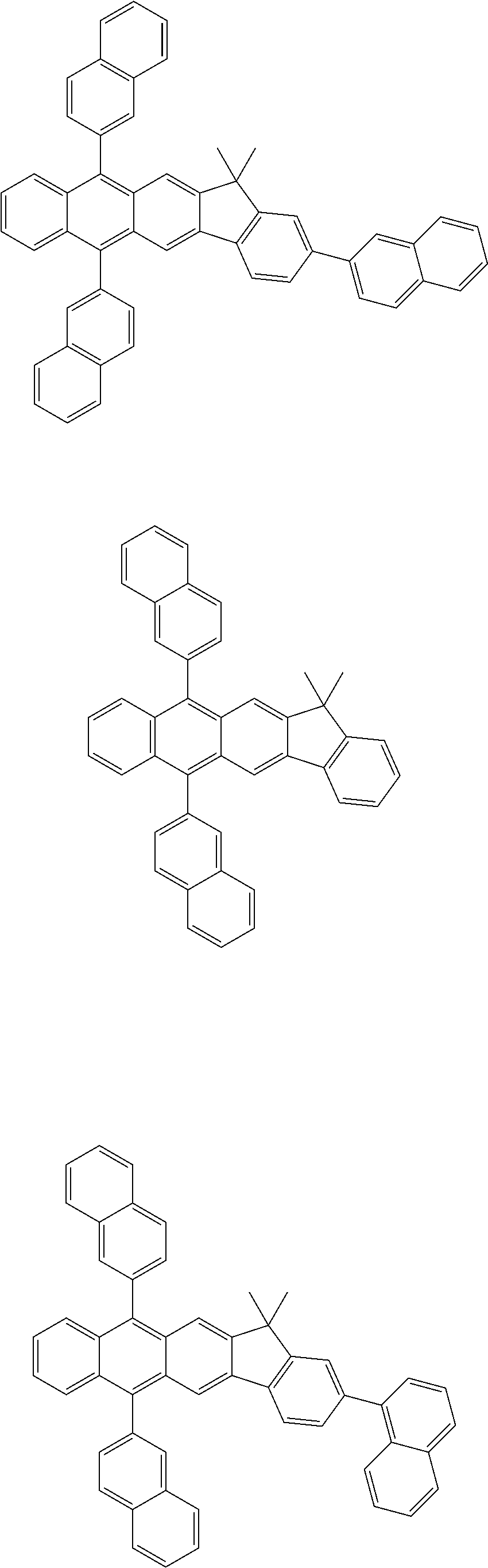


| TABLE 1 | ||
| Example | EML material | T97 lifetime (hr @ 100 mA/cm2) |
| Example 1 | Compound 1 | 970 |
| Example 2 | Compound 4 | 921 |
| Example 3 | Compound 6 | 943 |
| Example 4 | Compound 9 | 921 |
| Example 5 | Compound 10 | 991 |
| Example 6 | Compound 16 | 937 |
| Example 7 | Compound 17 | 897 |
| Example 8 | Compound 18 | 911 |
| Example 9 | Compound 19 | 956 |
| Example 10 | Compound 25 | 971 |
| Example 11 | Compound 29 | 923 |
| Comparative | CBP | 675 |
| Example 1 | ||
Claims (15)


Applications Claiming Priority (2)
| Application Number | Priority Date | Filing Date | Title |
|---|---|---|---|
| KR10-2012-0139820 | 2012-12-04 | ||
| KR1020120139820A KR102087950B1 (en) | 2012-12-04 | 2012-12-04 | Heterocyclic compound and organic light emitting device comprising the same |
Publications (2)
| Publication Number | Publication Date |
|---|---|
| US20140151650A1 US20140151650A1 (en) | 2014-06-05 |
| US9825233B2 true US9825233B2 (en) | 2017-11-21 |
Family
ID=50824560
Family Applications (1)
| Application Number | Title | Priority Date | Filing Date |
|---|---|---|---|
| US14/012,545 Active 2034-09-17 US9825233B2 (en) | 2012-12-04 | 2013-08-28 | Heterocyclic compound and organic light-emitting device including the same |
Country Status (2)
| Country | Link |
|---|---|
| US (1) | US9825233B2 (en) |
| KR (1) | KR102087950B1 (en) |
Families Citing this family (4)
| Publication number | Priority date | Publication date | Assignee | Title |
|---|---|---|---|---|
| KR102052071B1 (en) * | 2013-02-21 | 2019-12-05 | 삼성디스플레이 주식회사 | Organic light emitting device |
| CN108727366B (en) * | 2017-04-13 | 2021-04-30 | 北京鼎材科技有限公司 | Benzophenanthroline derivatives and application thereof |
| CN109134457A (en) * | 2017-06-28 | 2019-01-04 | 北京鼎材科技有限公司 | Benzo Féraud oxazoline derivates and its application |
| US11557733B2 (en) | 2018-03-12 | 2023-01-17 | Universal Display Corporation | Organic electroluminescent materials and devices |
Citations (12)
| Publication number | Priority date | Publication date | Assignee | Title |
|---|---|---|---|---|
| US20020158242A1 (en) | 1999-12-31 | 2002-10-31 | Se-Hwan Son | Electronic device comprising organic compound having p-type semiconducting characteristics |
| KR20040051507A (en) | 2002-12-11 | 2004-06-18 | 주식회사 엘지화학 | Electroluminescent devices with low work funciotn anode |
| US20060113905A1 (en) * | 2004-11-26 | 2006-06-01 | Norio Nakamura | Display device |
| US20060131562A1 (en) * | 2004-12-16 | 2006-06-22 | Au Optronics Corporation | Organic light-emitting device with improved layer structure |
| JP2007189001A (en) * | 2006-01-12 | 2007-07-26 | Konica Minolta Holdings Inc | ORGANIC ELECTROLUMINESCENT ELEMENT MATERIAL, ORGANIC ELECTROLUMINESCENT ELEMENT, DISPLAY DEVICE AND LIGHTING DEVICE |
| US20110108819A1 (en) * | 2008-08-18 | 2011-05-12 | Poopathy Kathirgamanathan | Compounds having electron transport properties, their preparation and use |
| KR20110092262A (en) | 2011-08-08 | 2011-08-17 | 덕산하이메탈(주) | Compound containing a hetero ring in the carbazole skeleton, and an organic electric device using the same, the terminal |
| US20110279020A1 (en) | 2010-04-20 | 2011-11-17 | Idemitsu Kosan Co., Ltd. | Biscarbazole Derivative, Material for Organic Electroluminescence Device and Organic Electroluminescence Device Using The Same |
| KR20120044529A (en) | 2010-10-28 | 2012-05-08 | 롬엔드하스전자재료코리아유한회사 | Novel organic electroluminescent compounds and organic electroluminescent device using the same |
| KR20120044517A (en) | 2010-10-28 | 2012-05-08 | 롬엔드하스전자재료코리아유한회사 | Novel compounds for organic electronic material and organic electroluminescent device using the same |
| US20140231759A1 (en) * | 2013-02-21 | 2014-08-21 | Samsung Display Co., Ltd. | Organic light-emitting diode |
| US9082988B2 (en) * | 2013-02-28 | 2015-07-14 | Samsung Display Co., Ltd. | Organic light emitting diode device |
Family Cites Families (1)
| Publication number | Priority date | Publication date | Assignee | Title |
|---|---|---|---|---|
| KR101971198B1 (en) * | 2011-10-19 | 2019-04-23 | 삼성디스플레이 주식회사 | Heterocyclic compound, organic light-emitting diode comprising the same, and flat display device comprising the organic light-emitting diode |
-
2012
- 2012-12-04 KR KR1020120139820A patent/KR102087950B1/en not_active Expired - Fee Related
-
2013
- 2013-08-28 US US14/012,545 patent/US9825233B2/en active Active
Patent Citations (14)
| Publication number | Priority date | Publication date | Assignee | Title |
|---|---|---|---|---|
| US20020158242A1 (en) | 1999-12-31 | 2002-10-31 | Se-Hwan Son | Electronic device comprising organic compound having p-type semiconducting characteristics |
| KR20040051507A (en) | 2002-12-11 | 2004-06-18 | 주식회사 엘지화학 | Electroluminescent devices with low work funciotn anode |
| US20060113905A1 (en) * | 2004-11-26 | 2006-06-01 | Norio Nakamura | Display device |
| US20060131562A1 (en) * | 2004-12-16 | 2006-06-22 | Au Optronics Corporation | Organic light-emitting device with improved layer structure |
| JP2007189001A (en) * | 2006-01-12 | 2007-07-26 | Konica Minolta Holdings Inc | ORGANIC ELECTROLUMINESCENT ELEMENT MATERIAL, ORGANIC ELECTROLUMINESCENT ELEMENT, DISPLAY DEVICE AND LIGHTING DEVICE |
| US20110108819A1 (en) * | 2008-08-18 | 2011-05-12 | Poopathy Kathirgamanathan | Compounds having electron transport properties, their preparation and use |
| KR20120034648A (en) | 2010-04-20 | 2012-04-12 | 이데미쓰 고산 가부시키가이샤 | Bis-carbazole derivative, material for organic electroluminescent element and organic electroluminescent element using same |
| US20110279020A1 (en) | 2010-04-20 | 2011-11-17 | Idemitsu Kosan Co., Ltd. | Biscarbazole Derivative, Material for Organic Electroluminescence Device and Organic Electroluminescence Device Using The Same |
| US20110278555A1 (en) | 2010-04-20 | 2011-11-17 | Idemitsu Kosan Co., Ltd. | Biscarbazole derivative, material for organic electroluminescence device and organic electroluminescence device using the same |
| KR20120044529A (en) | 2010-10-28 | 2012-05-08 | 롬엔드하스전자재료코리아유한회사 | Novel organic electroluminescent compounds and organic electroluminescent device using the same |
| KR20120044517A (en) | 2010-10-28 | 2012-05-08 | 롬엔드하스전자재료코리아유한회사 | Novel compounds for organic electronic material and organic electroluminescent device using the same |
| KR20110092262A (en) | 2011-08-08 | 2011-08-17 | 덕산하이메탈(주) | Compound containing a hetero ring in the carbazole skeleton, and an organic electric device using the same, the terminal |
| US20140231759A1 (en) * | 2013-02-21 | 2014-08-21 | Samsung Display Co., Ltd. | Organic light-emitting diode |
| US9082988B2 (en) * | 2013-02-28 | 2015-07-14 | Samsung Display Co., Ltd. | Organic light emitting diode device |
Also Published As
| Publication number | Publication date |
|---|---|
| KR20140071805A (en) | 2014-06-12 |
| US20140151650A1 (en) | 2014-06-05 |
| KR102087950B1 (en) | 2020-03-12 |
Similar Documents
| Publication | Publication Date | Title |
|---|---|---|
| US11063220B2 (en) | Organic light-emitting device | |
| US9455409B2 (en) | Amine-based compound and organic light emitting device including the same | |
| US9136480B2 (en) | Organic light-emitting diode | |
| US9276227B2 (en) | Organic light-emitting device and flat panel display including the same | |
| US9722182B2 (en) | Heterocyclic compound and organic light-emitting device including the same | |
| US8920946B2 (en) | Organic light-emitting compound and organic light-emitting device including the same | |
| US9385325B2 (en) | Heterocyclic compound and organic light emitting device including the same | |
| KR102052071B1 (en) | Organic light emitting device | |
| US9502663B2 (en) | Heterocyclic compound and organic light emitting device comprising the same | |
| US9666809B2 (en) | Compound and organic light-emitting device including the same | |
| US8999528B2 (en) | Condensation compound and organic light emitting device including the same | |
| US9761808B2 (en) | Heterocyclic compound and organic light-emitting device comprising the same | |
| KR102278600B1 (en) | Compound and organic light emitting device comprising same | |
| US9825233B2 (en) | Heterocyclic compound and organic light-emitting device including the same | |
| US9741935B2 (en) | Organic light-emitting device | |
| US9634257B2 (en) | Heterocyclic compound and organic light-emitting device including the same | |
| US9741947B2 (en) | Organometallic complex and organic light-emitting device including the same | |
| US9416107B2 (en) | Heterocyclic compound and organic light-emitting device including the same | |
| US9362507B2 (en) | Compound and organic light-emitting diode including the same | |
| US20140291634A1 (en) | Indole-based compound and organic light-emitting diode comprising the same | |
| KR102116492B1 (en) | Compound and organic light emitting device comprising the same | |
| US9444056B2 (en) | Heterocyclic compound and organic light-emitting device including the same |
Legal Events
| Date | Code | Title | Description |
|---|---|---|---|
| AS | Assignment |
Owner name: SAMSUNG DISPLAY CO., LTD., KOREA, REPUBLIC OF Free format text: ASSIGNMENT OF ASSIGNORS INTEREST;ASSIGNOR:LEE, JUNG-SUB;REEL/FRAME:032776/0242 Effective date: 20130624 |
|
| STCF | Information on status: patent grant |
Free format text: PATENTED CASE |
|
| MAFP | Maintenance fee payment |
Free format text: PAYMENT OF MAINTENANCE FEE, 4TH YEAR, LARGE ENTITY (ORIGINAL EVENT CODE: M1551); ENTITY STATUS OF PATENT OWNER: LARGE ENTITY Year of fee payment: 4 |
|
| MAFP | Maintenance fee payment |
Free format text: PAYMENT OF MAINTENANCE FEE, 8TH YEAR, LARGE ENTITY (ORIGINAL EVENT CODE: M1552); ENTITY STATUS OF PATENT OWNER: LARGE ENTITY Year of fee payment: 8 |