US9824942B2 - Method of manufacturing thin-film transistor substrate including a copper alloy film - Google Patents
Method of manufacturing thin-film transistor substrate including a copper alloy film Download PDFInfo
- Publication number
- US9824942B2 US9824942B2 US15/304,060 US201415304060A US9824942B2 US 9824942 B2 US9824942 B2 US 9824942B2 US 201415304060 A US201415304060 A US 201415304060A US 9824942 B2 US9824942 B2 US 9824942B2
- Authority
- US
- United States
- Prior art keywords
- film
- alloy film
- cumn alloy
- thin
- cumn
- Prior art date
- Legal status (The legal status is an assumption and is not a legal conclusion. Google has not performed a legal analysis and makes no representation as to the accuracy of the status listed.)
- Active
Links
Images


Classifications
-
- H01L22/20—
-
- H—ELECTRICITY
- H10—SEMICONDUCTOR DEVICES; ELECTRIC SOLID-STATE DEVICES NOT OTHERWISE PROVIDED FOR
- H10P—GENERIC PROCESSES OR APPARATUS FOR THE MANUFACTURE OR TREATMENT OF DEVICES COVERED BY CLASS H10
- H10P74/00—Testing or measuring during manufacture or treatment of wafers, substrates or devices
- H10P74/23—Testing or measuring during manufacture or treatment of wafers, substrates or devices characterised by multiple measurements, corrections, marking or sorting processes
-
- G—PHYSICS
- G09—EDUCATION; CRYPTOGRAPHY; DISPLAY; ADVERTISING; SEALS
- G09F—DISPLAYING; ADVERTISING; SIGNS; LABELS OR NAME-PLATES; SEALS
- G09F9/00—Indicating arrangements for variable information in which the information is built-up on a support by selection or combination of individual elements
- G09F9/30—Indicating arrangements for variable information in which the information is built-up on a support by selection or combination of individual elements in which the desired character or characters are formed by combining individual elements
-
- H01L21/02068—
-
- H01L21/28—
-
- H01L21/441—
-
- H01L29/45—
-
- H01L29/66969—
-
- H01L29/786—
-
- H01L29/7869—
-
- H01L51/50—
-
- H—ELECTRICITY
- H10—SEMICONDUCTOR DEVICES; ELECTRIC SOLID-STATE DEVICES NOT OTHERWISE PROVIDED FOR
- H10D—INORGANIC ELECTRIC SEMICONDUCTOR DEVICES
- H10D30/00—Field-effect transistors [FET]
- H10D30/60—Insulated-gate field-effect transistors [IGFET]
- H10D30/67—Thin-film transistors [TFT]
-
- H—ELECTRICITY
- H10—SEMICONDUCTOR DEVICES; ELECTRIC SOLID-STATE DEVICES NOT OTHERWISE PROVIDED FOR
- H10D—INORGANIC ELECTRIC SEMICONDUCTOR DEVICES
- H10D30/00—Field-effect transistors [FET]
- H10D30/60—Insulated-gate field-effect transistors [IGFET]
- H10D30/67—Thin-film transistors [TFT]
- H10D30/6729—Thin-film transistors [TFT] characterised by the electrodes
-
- H—ELECTRICITY
- H10—SEMICONDUCTOR DEVICES; ELECTRIC SOLID-STATE DEVICES NOT OTHERWISE PROVIDED FOR
- H10D—INORGANIC ELECTRIC SEMICONDUCTOR DEVICES
- H10D30/00—Field-effect transistors [FET]
- H10D30/60—Insulated-gate field-effect transistors [IGFET]
- H10D30/67—Thin-film transistors [TFT]
- H10D30/674—Thin-film transistors [TFT] characterised by the active materials
- H10D30/6755—Oxide semiconductors, e.g. zinc oxide, copper aluminium oxide or cadmium stannate
-
- H—ELECTRICITY
- H10—SEMICONDUCTOR DEVICES; ELECTRIC SOLID-STATE DEVICES NOT OTHERWISE PROVIDED FOR
- H10D—INORGANIC ELECTRIC SEMICONDUCTOR DEVICES
- H10D64/00—Electrodes of devices having potential barriers
- H10D64/01—Manufacture or treatment
- H10D64/011—Manufacture or treatment of electrodes ohmically coupled to a semiconductor
-
- H—ELECTRICITY
- H10—SEMICONDUCTOR DEVICES; ELECTRIC SOLID-STATE DEVICES NOT OTHERWISE PROVIDED FOR
- H10D—INORGANIC ELECTRIC SEMICONDUCTOR DEVICES
- H10D64/00—Electrodes of devices having potential barriers
- H10D64/60—Electrodes characterised by their materials
- H10D64/62—Electrodes ohmically coupled to a semiconductor
-
- H—ELECTRICITY
- H10—SEMICONDUCTOR DEVICES; ELECTRIC SOLID-STATE DEVICES NOT OTHERWISE PROVIDED FOR
- H10D—INORGANIC ELECTRIC SEMICONDUCTOR DEVICES
- H10D86/00—Integrated devices formed in or on insulating or conducting substrates, e.g. formed in silicon-on-insulator [SOI] substrates or on stainless steel or glass substrates
- H10D86/40—Integrated devices formed in or on insulating or conducting substrates, e.g. formed in silicon-on-insulator [SOI] substrates or on stainless steel or glass substrates characterised by multiple TFTs
- H10D86/441—Interconnections, e.g. scanning lines
-
- H—ELECTRICITY
- H10—SEMICONDUCTOR DEVICES; ELECTRIC SOLID-STATE DEVICES NOT OTHERWISE PROVIDED FOR
- H10D—INORGANIC ELECTRIC SEMICONDUCTOR DEVICES
- H10D86/00—Integrated devices formed in or on insulating or conducting substrates, e.g. formed in silicon-on-insulator [SOI] substrates or on stainless steel or glass substrates
- H10D86/40—Integrated devices formed in or on insulating or conducting substrates, e.g. formed in silicon-on-insulator [SOI] substrates or on stainless steel or glass substrates characterised by multiple TFTs
- H10D86/60—Integrated devices formed in or on insulating or conducting substrates, e.g. formed in silicon-on-insulator [SOI] substrates or on stainless steel or glass substrates characterised by multiple TFTs wherein the TFTs are in active matrices
-
- H—ELECTRICITY
- H10—SEMICONDUCTOR DEVICES; ELECTRIC SOLID-STATE DEVICES NOT OTHERWISE PROVIDED FOR
- H10D—INORGANIC ELECTRIC SEMICONDUCTOR DEVICES
- H10D99/00—Subject matter not provided for in other groups of this subclass
-
- H—ELECTRICITY
- H10—SEMICONDUCTOR DEVICES; ELECTRIC SOLID-STATE DEVICES NOT OTHERWISE PROVIDED FOR
- H10P—GENERIC PROCESSES OR APPARATUS FOR THE MANUFACTURE OR TREATMENT OF DEVICES COVERED BY CLASS H10
- H10P70/00—Cleaning of wafers, substrates or parts of devices
- H10P70/20—Cleaning during device manufacture
- H10P70/27—Cleaning during device manufacture during, before or after processing of conductive materials, e.g. polysilicon or amorphous silicon layers
-
- H—ELECTRICITY
- H10—SEMICONDUCTOR DEVICES; ELECTRIC SOLID-STATE DEVICES NOT OTHERWISE PROVIDED FOR
- H10P—GENERIC PROCESSES OR APPARATUS FOR THE MANUFACTURE OR TREATMENT OF DEVICES COVERED BY CLASS H10
- H10P74/00—Testing or measuring during manufacture or treatment of wafers, substrates or devices
- H10P74/20—Testing or measuring during manufacture or treatment of wafers, substrates or devices characterised by the properties tested or measured, e.g. structural or electrical properties
- H10P74/203—Structural properties, e.g. testing or measuring thicknesses, line widths, warpage, bond strengths or physical defects
Definitions
- the present disclosure relates to a method of manufacturing a thin-film transistor substrate.
- Active matrix display devices such as liquid crystal display devices and organic electroluminescent (EL) display devices, include a thin-film transistor (TFT) substrate in which TFTs are formed as switching elements or drive elements.
- TFT thin-film transistor
- PTL Patent Literature 1 describes an active matrix organic EL display device including a TFT substrate.
- Structures of the TFT include a bottom-gate TFT in which a gate electrode is disposed in a lower part (substrate side) of a channel layer, and a top-gate TFT in which a gate electrode is disposed in an upper part of the channel layer.
- a silicon semiconductor or an oxide semiconductor is used as the channel layer of the TFT.
- TFT substrate TFT array substrate which includes a plurality of pixels arranged in a matrix, a plurality of lines through which a signal (voltage) for driving each of the pixels is transmitted are disposed.
- the lines are formed using the same materials as materials of a source electrode or a drain electrode of the TFT and in the same layer as the source electrode or the drain electrode of the TFT. For that reason, the source electrode or the drain electrode is required to have a function of not only the TFT but also the line.
- Cu has low adhesion to an insulating film (interlayer insulation film) of a silicon oxide etc.
- a technique of forming a Cu alloy film such as a CuMn film between a Cu line or a Cu electrode and the insulating film has been proposed (for example, PTL 1).
- a line or an electrode which is covered by an insulating film is electrically connected to other electrodes or lines via a contact hole formed through the insulating film.
- an insulating film interlayer insulation film
- a contact hole is formed through an insulating film on the CuMn alloy film to expose a surface of the CuMn alloy film, and a conductive film is formed on the insulating film to cover the contact hole, thereby causing the CuMn alloy film and the conductive film to be in contact with each other.
- the technique disclosed herein has an object of providing a TFT substrate with desired performance.
- one aspect of a method of manufacturing a thin-film transistor substrate according to the present disclosure is a method of manufacturing a thin-film transistor substrate including a thin-film transistor having a CuMn alloy film, the method including: forming the CuMn alloy film; and controlling a contact resistance of a surface of the CuMn alloy film on a basis of a contact angle of the surface of the CuMn alloy film.
- FIG. 1 is a partially cutaway perspective view of an organic EL display device according to an embodiment.
- FIG. 2 is a perspective view illustrating an example of pixel banks of the organic EL display device according to the embodiment.
- FIG. 3 is an electrical circuit diagram illustrating the structure of a pixel circuit in the organic EL display device according to the embodiment.
- FIG. 4 is a schematic sectional view of a TFT substrate according to the embodiment.
- FIG. 5 is a schematic sectional view of a TFT substrate according to another embodiment.
- FIG. 6 is a diagram illustrating a relationship between a CuMn surface exposure time and a contact resistance in a CuMn alloy film and an ITO film.
- FIG. 7 is a diagram illustrating a relationship between the CuMn surface exposure time and a contact angle of a surface of the CuMn alloy film in the CuMn alloy film and the ITO film.
- FIG. 8 is a diagram illustrating a result of analyzing the peak separation of Cu2p3/2 spectrum by X-ray photoemission spectroscopy (XPS) in the CuMn alloy film.
- XPS X-ray photoemission spectroscopy
- FIG. 9A is a diagram illustrating changes in an abundance ratio of CuO over exposure time.
- FIG. 9B is a diagram illustrating changes in an abundance ratio of metal Cu or Cu 2 O over exposure time.
- FIG. 9C is a diagram illustrating changes in an abundance ratio of Cu(OH) 2 over exposure time.
- FIG. 10 is a diagram illustrating a relationship between a contact angle of a surface of a CuMn alloy film and a contact resistance of the surface of the CuMn alloy film.
- FIG. 11A is a sectional view illustrating a process of forming a gate electrode (first wiring layer) in a method of manufacturing the TFT substrate according to the embodiment.
- FIG. 11B is a sectional view illustrating a process of forming a first insulating film (gate insulating film) in the method of manufacturing the TFT substrate according to the embodiment.
- FIG. 11C is a sectional view illustrating a process of forming an oxide semiconductor layer in the method of manufacturing the TFT substrate according to the embodiment.
- FIG. 11D is a sectional view illustrating a process of forming a second insulating film in the method of manufacturing the TFT substrate according to the embodiment.
- FIG. 11E is a sectional view illustrating a process of forming a contact hole in the method of manufacturing the TFT substrate according to the embodiment.
- FIG. 11F is a sectional view illustrating a process of forming a source drain electrode (second wiring layer) in a method of manufacturing the TFT substrate according to the embodiment.
- FIG. 11G is a sectional view illustrating a process of forming a third insulating film in the method of manufacturing the TFT substrate according to the embodiment.
- FIG. 11H is a sectional view illustrating a process of forming a resist film in the method of manufacturing the TFT substrate according to the embodiment.
- FIG. 11I is a sectional view illustrating a process of forming a resist film patterning in the method of manufacturing the TFT substrate according to the embodiment.
- FIG. 11J is a sectional view illustrating a process of forming a contact hole in the method of manufacturing the TFT substrate according to the embodiment.
- FIG. 11K is a sectional view illustrating a process of removing a resist film in the method of manufacturing the TFT substrate according to the embodiment.
- FIG. 11L is a sectional view illustrating a process of measuring a contact angle in the method of manufacturing the TFT substrate according to the embodiment.
- FIG. 11M is a sectional view illustrating a process of forming a third wiring layer in the method of manufacturing the TFT substrate according to the embodiment.
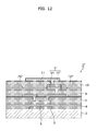
- FIG. 12 is a schematic sectional view of a TFT substrate according to a modification example.
- each of the diagrams is a schematic diagram and thus is not necessarily strictly illustrated.
- substantially the same structural components are assigned with the same reference signs, and redundant descriptions will be omitted or simplified.
- an organic EL display device shall be described as an example of a display device which includes a TFT substrate.
- FIG. 1 is a partially cutaway perspective view of an organic EL display device according to an embodiment.
- FIG. 2 is a perspective view of an example of pixel banks of the organic EL display device according to the embodiment.
- the organic EL display device 100 has a stack structure of a TFT substrate (TFT array substrate) 1 and an organic EL element (light emitting part) 130 .
- the TFT substrate 1 has a plurality of thin-film transistors arranged therein.
- the organic EL element 130 includes an anode 131 which is a lower electrode, an EL layer 132 which is a light emitting layer formed of an organic material, and a cathode 133 which is a transparent upper electrode.
- the organic EL display device 100 is a top emission type, and the anode 131 is a reflection electrode. It should be noted that the organic EL display device 100 is not limited to the top emission type, and may be a bottom emission type.
- a plurality of pixels 110 are arranged in the TFT substrate 1 in a matrix. Each pixel 110 is provided with a pixel circuit 120 .
- the organic EL element 130 is formed in association with each of the plurality of pixels 110 .
- the pixel circuit 120 in each pixel 110 controls the light emission of the corresponding organic EL element 130 .
- the organic EL elements 130 are formed on an interlayer insulation film (planarizing layer) that is formed to cover the plurality of thin-film transistors.
- Each organic EL element 130 has the EL layer 132 between the anode 131 and the cathode 133 .
- a hole transport layer is disposed between the anode 131 and the EL layer 132
- an electron transport layer is disposed between the EL layer 132 and the cathode 133 .
- any other functional layer(s) may be disposed between the anode 131 and the cathode 133 .
- Each pixel 110 is driven by the corresponding pixel circuit 120 .
- a plurality of gate lines (scan lines) 140 are arranged along the row direction of the pixels 110
- a plurality of source lines (signal lines) 150 are arranged along the column direction of the pixels 110 so as to intersect with the gate lines 140
- a plurality of power lines are arranged in parallel with the source lines 150 .
- the pixels 110 are defined by, for example, the gate lines 140 and source lines 150 orthogonal to each other.
- the gate lines 140 are each connected to the gate electrode of the thin-film transistor included in each pixel circuit 120 and operating as a switching element, on a row-by-row basis.
- the source lines 150 are each connected to the source electrode of the thin-film transistor included in each pixel circuit 120 and operating as a switching element, on a column-by-column basis.
- the power lines are each connected to the drain electrode of the thin-film transistor included in each pixel circuit 120 and operating as a drive element, on a column-by-column basis.
- each pixel 110 in the organic EL display device 100 is composed of subpixels 110 R, 110 G, and 110 B of three colors (red, green, blue).
- the plurality of subpixels 110 R, 110 G, and 110 B are arranged on a display surface in the form of a matrix.
- the subpixels 110 R, 110 G, and 110 B are separated from each other by banks 111 .
- the banks 111 are formed in a grid so that projections lying in parallel with the gate lines 140 and projections lying in parallel with the source lines 150 intersect with each other.
- the portions enclosed by the projections (i.e. the openings of the banks 111 ) and the subpixels 110 R, 110 G, and 110 B are in a one-to-one correspondence with each other.
- the banks 111 are pixel banks in this embodiment, the banks 111 may be line banks.
- the anode 131 is formed on the interlayer insulation film (planarizing layer) on the TFT substrate 1 and in the opening of the bank 111 , for each of the subpixels 110 R, 110 G, and 110 B.
- the EL layer 132 is formed on the anode 131 and in the opening of the bank 111 , for each of the subpixels 110 R, 110 G, and 110 B.
- the transparent cathode 133 is formed continuously on the plurality of banks 111 so as to cover all EL layers 132 (all subpixels 110 R, 110 G, and 110 B).
- the pixel circuit 120 is provided for each of the subpixels 110 R, 110 G, and 110 B.
- Each of the subpixels 110 R, 110 G, and 110 B and its corresponding pixel circuit 120 are electrically connected to each other by a contact hole and a relay electrode. It should be noted that the subpixels 110 R, 110 G, and 110 B have the same structure except that the respective EL layers 132 emit different colors of light.
- FIG. 3 is an electrical circuit diagram illustrating the structure of a pixel circuit in the organic EL display device according to the embodiment.
- the pixel circuit 120 includes a thin-film transistor SwTr that operates as a switching element, a thin-film transistor DrTr that operates as a drive element, and a capacitor C that stores data to be displayed at the corresponding pixel 110 .
- the thin-film transistor SwTr is a switching transistor for selecting the pixel 110
- the thin-film transistor DrTr is a drive transistor for driving the organic EL element 130 .
- the thin-film transistor SwTr has a gate electrode G 1 connected to the gate line 140 , a source electrode S 1 connected to the source line 150 , a drain electrode D 1 connected to the capacitor C and the gate electrode G 2 of the thin-film transistor DrTr, and a semiconductor film (not illustrated).
- a predetermined voltage is applied to the gate line 140 and the source line 150 to which the thin-film transistor SwTr is connected, the voltage applied to the source line 150 is stored in the capacitor C as a data voltage.
- the thin-film transistor DrTr has a gate electrode G 2 connected to the drain electrode D 1 of the thin-film transistor SwTr and the capacitor C, a drain electrode D 2 connected to the power line 160 and the capacitor C, a source electrode S 2 connected to the anode 131 of the organic EL element 130 , and a semiconductor film (not illustrated).
- the thin-film transistor DrTr supplies the current corresponding to the data voltage stored in the capacitor C, from the power line 160 to the anode 131 of the organic EL element 130 via the source electrode S 2 .
- the drive current flows from the anode 131 to cathode 133 in the organic EL element 130 , and the EL layer 132 emits light.
- the organic EL display device 100 having the structure described above is an active matrix display device which controls display for each pixel 110 located at a different one of the intersections of the gate lines 140 and source lines 150 .
- the thin-film transistor SwTr and the thin-film transistor DrTr in each pixel 110 cause the corresponding organic EL element 130 to emit light selectively, as a result of which a desired image is displayed.
- FIG. 4 is a schematic sectional view of the TFT substrate according to the embodiment.
- the TFT substrate 1 in the aforementioned organic EL display device 100 is described in the following embodiment.
- the thin-film transistor Tr according to the embodiment is applicable to both the above-described thin-film transistor SWTr (switching transistor) and the above-described thin-film transistor DrTr (drive transistor).
- the TFT substrate 1 includes: a substrate 2 ; a gate electrode 3 ; a gate insulating film 4 (first insulating film); an oxide semiconductor layer 5 ; an insulating layer 6 (second insulating film); a source electrode 7 S; a drain electrode 7 D; an insulating layer 8 (third insulating film); and an upper-layer wiring 9 .
- the gate electrode 3 , the source electrode 7 S and the drain electrode 7 D, and the upper-layer wiring 9 are each formed of a metal material, and a layer in which each of these electrodes and the line is formed is a metal layer (wiring layer). More specifically, the layer in which the gate electrode 3 is formed is the first wiring layer (first metal layer), the layer in which the source electrode 7 S and the drain electrode 7 D are formed is the second wiring layer (second metal layer), and the layer in which the upper-layer wiring 9 is formed is the third wiring layer (third metal layer).
- the TFT substrate 1 has three wiring layers, and each metal layer can be used as a wiring layer for forming various lines. More specifically, by patterning a metal film (conductive film) formed on each metal layer into a predetermined shape, it is possible to form a desired interconnecting line or electrode having a predetermined shape, in addition to the above-described electrodes and line.
- a metal film conductive film
- the gate line 140 , the source line 150 , and the power line 160 illustrated in FIG. 1 are formed in each of the metal layer.
- a contact hole is formed through an insulating layer between the upper and lower metal layers, for connecting the lines in each of the metal layers, or for connecting the lines and the electrodes.
- the thin-film transistor Tr includes: the gate electrode 3 ; the gate insulating film 4 ; the oxide semiconductor layer 5 ; the source electrode 7 S, and the drain electrode 7 D, in the TFT substrate 1 .
- the gate electrode 3 , the source electrode 7 S, and the drain electrode 7 D correspond to the gate electrode G 2 , the source electrode S 2 , and the drain electrode D 2 in FIG. 3 , respectively.
- the thin-film transistor Tr according to the present embodiment is a bottom-gate TFT.
- TFT substrate 1 Each structural component in the TFT substrate 1 is described in detail below, with reference to FIG. 4 .
- the substrate 2 is a glass substrate such as a G 8 substrate, for example. It should be noted that the substrate 2 may be a flexible substrate such as a resin substrate. An undercoat layer may be formed on the surface of the substrate 2 .
- the gate electrode 3 is formed in a predetermined shape, above the substrate 2 .
- a metal such as titanium (Ti), molybdenum (Mo), tungsten (W), aluminum (Al), gold (Au), and copper (Cu), or a conductive oxide such as indium tin oxide (ITO) is used.
- an alloy such as a molybdenumtungsten alloy (MoW) may be used as the gate electrode 3 .
- a stack structure in which a metal such as Ti, Al, or Au as metal having good adhesion to an oxide is sandwiched may be used as the gate electrode 3 .
- the gate insulating layer 4 is formed between the gate electrode 3 and the oxide semiconductor layer 5 .
- the gate insulating film 4 is formed above the substrate 2 to cover the gate electrode 3 .
- the gate insulation film 4 is, for example, a single-layer film of an oxide thin film such as a silicon oxide film or a hafnium oxide film, a nitride film such as a silicon nitride film, or a silicon oxynitride film, or a stack of these films.
- the oxide semiconductor layer 5 is formed in a predetermined shape, above the substrate 2 .
- the oxide semiconductor layer 5 is the channel layer (semiconductor layer) of the thin-film transistor Tr, and faces the gate electrode 3 .
- the oxide semiconductor layer 5 is formed in the shape of an island on the gate insulating layer 4 above gate electrode 3 .
- the oxide semiconductor layer 5 is desirably made of a transparent amorphous oxide semiconductor (TAOS) such as InGaZnO x (IGZO) containing In—Ga—Zn—O.
- TAOS transparent amorphous oxide semiconductor
- IGZO InGaZnO x
- a thin-film transistor having the transparent amorphous oxide semiconductor as its channel layer has high carrier mobility, and is suitable for large-screen, high-resolution display devices.
- the transparent amorphous oxide semiconductor is also capable of low-temperature deposition, and so can be formed easily on a flexible substrate.
- the amorphous oxide semiconductor of InGaZnO x can be deposited by vapor-phase deposition such as sputtering or laser deposition using, as a target, a polycrystalline sintered body having a composition of InGaO 3 (ZnO) 4 .
- the insulating layer 6 is deposited on the gate insulating layer 4 to cover the oxide semiconductor layer 5 .
- the oxide semiconductor layer 5 is covered by the insulating layer 6 , and the insulating layer 6 serves as a protection layer (channel protection layer) which protects the oxide semiconductor layer 5 .
- the insulating layer 6 is, for example, a single-layer film such as a silicon oxide (SiO 2 ) film or an aluminum oxide (A 1 2 O 3 ) film, or a stack of these oxide films.
- a portion of the insulating layer 6 has an opening that passes through the insulating layer 6 , and the oxide semiconductor layer 5 is connected to the source electrode 7 S and the drain electrode 7 D via the opening (contact hole).
- the source electrode 7 S and the drain electrode 7 D are formed in a predetermined shape on the insulating layer 6 . More specifically, the source electrode 7 S and the drain electrode 7 D are connected to the oxide semiconductor layer 5 via contact holes provided in the insulating layer 6 , and disposed on the insulating layer 6 opposite each other at predetermined intervals in the horizontal direction of the substrate.
- the source electrode 7 S and the drain electrode 7 D each include copper (Cu) as a main component, and have a stack structure of a copper film (Cu film) and a copper-manganese alloy film (CuMn alloy film).
- the source electrode 7 S is a stacked film formed by stacking a first film 71 S that is the Cu film and a second film 72 S that is the CuMn alloy film in this order from bottom to top.
- the drain electrode 7 D is a stacked film formed by stacking a first film 71 D that is the Cu film and a second film 72 D that is the CuMn alloy film in this order from bottom to top. It should be noted that the first films 71 S and 71 D which are the Cu films may preferably have a thickness greater than a thickness of the second films 72 S and 72 D.
- the use of a Cu film that is a low-resistance material as the source electrode 7 S and the drain electrode 7 D contributes to lower resistance of the source electrode 7 S and the drain electrode 7 D, and also contributes to lower resistance of a line formed on the second metal layer (line on the same layer as the source electrode 7 S and the drain electrode 7 D).
- the CuMn alloy film as described herein is an alloy film of copper and manganese.
- the insulating layer 8 is formed on the insulating layer 6 to cover the source electrode 7 S and the drain electrode 7 D.
- the insulating layer 8 is, for example, a single-layer film such as a silicon oxide (SiO 2 ) film or an aluminum oxide (Al 2 O 3 ) film, or a stack of these oxide films.
- the upper-layer wiring 9 is formed of a conductive film formed in a predetermined shape on the insulating layer 8 , and connected to the drain electrode 7 D via a contact hole formed through the insulating layer 8 .
- the upper-layer wiring 9 according to the present embodiment is an ITO film formed of ITO.
- the TFT substrate 1 according to the present embodiment is configured as described above. It should be noted that, although the source electrode 7 S and the drain electrode 7 D each have a two-layer structure of the CuMn alloy film and the Cu film according to the present embodiment, the present disclosure is not limited to this example.
- a TFT substrate 1 ′ including the source electrode 7 S′ and the drain electrode 7 D′ each having a three-layer structure may be exemplified.
- the source electrode 7 S′ may be a stacked film of a third film 73 S that is an Mo (molybdenum) film or the CuMn film, a first film 71 S that is the Cu film, and a second film 72 S that is the CuMn alloy film.
- the drain electrode 7 D′ may be a stacked film of a third film 73 D that is the Mo film or the CuMn film, a first film 71 D that is the Cu film, and a second film 72 D that is the CuMn alloy film.
- the use of the CuMn film or the Mo film as the undermost layer of the source electrode 7 S′ and the drain electrode 7 D′ it is possible to decrease the possibility that Cu atoms in the second film (Cu film) diffuses into the layer under the second film, and also to enhance adhesion to the underlayer.
- a contact hole is formed through the insulating film (interlayer insulating film).
- the insulating film interlayer insulating film
- an ITO film in the wiring layer of an upper layer is to be formed on the CuMn alloy film in the wiring layer of a lower layer via the contact hole in the insulating film
- a surface of the CuMn alloy film is exposed.
- the second film 72 D (CuMn alloy film) of the drain electrode 7 D and the upper-layer wiring 9 (ITO film) are to be connected, a surface of the second film 72 D is exposed after a contact hole is formed through the insulating layer 8 .
- a contact resistance between the ITO film and the CuMn alloy film increases with an increase in wait time from when the CuMn alloy film (second film 72 D) is exposed to when the CuMn alloy film is covered by the ITO film (upper-layer wiring 9 ). This leads to a decrease in uniformity or reliability of display of the display panel.
- the above-described change in the contact resistance is caused by oxidation of the exposed surface of the CuMn alloy film which occurs during the wait time before deposition of the ITO film.
- no conventional technique of observing the change in the contact resistance has been available as an in-line process, and thus it has not been possible to control the contact resistance of the surface of the CuMn alloy film. For that reason, it has been difficult to implement a TFT substrate with desired performance.
- FIG. 6 is a diagram illustrating a relationship between the CuMn surface exposure time and the contact resistance in the CuMn alloy film and an ITO film.
- the contact resistance increases with an increase in the CuMn surface exposure time until the CuMn surface exposure time reaches a certain amount of time (approximately 60 hours), and the contact resistance is substantially unchanged after the CuMn surface exposure time exceeds the above-described certain amount of time (approximately 60 hours).
- the CuMn surface exposure time is a time period starting from removing a resist film when forming a contact hole through the insulating film (insulating layer 8 ) that covers the CuMn alloy film.
- the contact resistance is measured after the ITO film is deposited on the CuMn alloy film. More specifically, the contact resistance of the second film 72 D (CuMn alloy film) of each of the drain electrodes 7 D of the plurality of thin-film transistors Tr in the TFT substrate 1 illustrated in FIG. 4 is measured using a contact chain.
- FIG. 7 is a diagram illustrating a relationship between the CuMn surface exposure time and the contact angle of the surface of the CuMn alloy film in the CuMn alloy film and the ITO film.
- the contact angle increases with an increase in the CuMn surface exposure time until the CuMn surface exposure time reaches a certain amount of time (approximately 60 hours), and the contact angle is substantially unchanged after the CuMn surface exposure time exceeds the above-described certain amount of time (approximately 60 hours).
- the contact angle is a contact angle with respect to water, and measured using a contact angle gauge.
- the inventor has also analyzed not the surface condition (contact angle) but an atom binding condition (composition change) of the CuMn alloy film. This also shall be described below with reference to FIG. 8 and FIG. 9A to FIG. 9C .
- FIG. 8 illustrates a result of the calculation.
- FIG. 8 is a diagram illustrating a result of analyzing the peak separation of Cu2p3/2 spectrum by XPS in the CuMn alloy film.
- FIG. 9A to FIG. 9C illustrate the results.
- FIG. 9A is a diagram illustrating changes in the abundance ratio of CuO over exposure time.
- FIG. 9B is a diagram illustrating changes in the abundance ratio of metal Cu or Cu 2 O over exposure time.
- FIG. 9C is a diagram illustrating changes in the abundance ratio of Cu(OH) 2 over exposure time. It should be noted that the exposure time in each of FIG. 9A to FIG. 9C is the above-described CuMn surface exposure time, and an elapsed time of exposure to atmosphere following removing the resist film when the contact hole is formed through the insulating film that covers the CuMn alloy film.
- FIG. 10 is a diagram illustrating a relationship between the contact angle of the surface of the CuMn alloy film and the contact resistance of the surface of the CuMn alloy film.
- the present invention has been conceived on the basis of a new knowledge that there is a correlation between the contact angle of the surface of the CuMn alloy film and the contact resistance of the surface of the CuMn alloy film, and the inventor has found out, by monitoring the contact angle of the surface of the CuMn alloy film, that it is possible to control the contact resistance of the surface of the CuMn alloy film.
- the contact resistance of the surface of the CuMn alloy film is controlled by measuring the contact angle of the surface of the CuMn alloy film, and, on the basis of a pre-measured and pre-calculated correlation (for example, FIG. 10 ), as reference data, between the contact angle of the CuMn alloy film and a contact resistance of the surface of the CuMn alloy film, determining whether or not the contact angle of the CuMn alloy film obtained by actually measuring in a manufacturing process of a TFT substrate is less than or equal to a predetermined value.
- FIG. 11A to FIG. 11M are cross-sectional views showing respective processes in the method of manufacturing the thin-film transistor substrate according to the embodiment.
- the method of manufacturing the TFT substrate 1 according to the present embodiment is a method of manufacturing a TFT substrate including a TFT having a CuMn alloy film, and includes a control process in which a contact resistance of a surface of the CuMn alloy film is controlled on the basis of a contact angle of the surface of the CuMn alloy film.
- a substrate 2 is prepared, and a gate electrode 3 is formed in a predetermined shape above the substrate 2 .
- a gate metal film is deposited on the substrate 2 of a G 8 glass substrate by sputtering, and the deposited gate metal film is processed by photolithography and wet etching to form the gate electrode 3 in a predetermined shape.
- a gate insulating film 4 is formed above the substrate 2 .
- the gate insulating film 4 made of a silicon oxide is deposited by plasma CVD, etc., so as to cover the gate electrode 3 .
- an oxide semiconductor layer 5 is formed into a predetermined shape above the substrate 2 .
- the oxide semiconductor layer 5 is formed on the gate insulating film 4 .
- a transparent amorphous oxide semiconductor of InGaZnO x is deposited on the gate insulating film 4 by sputtering or the like, and the deposited transparent amorphous oxide semiconductor is processed by photolithography and etching, to form the oxide semiconductor layer 5 in the predetermined shape above the gate electrode 3 .
- an insulating layer 6 is deposited on the gate insulating layer 4 to cover the oxide semiconductor layer 5 , as illustrated in FIG. 11D .
- the insulating layer 6 formed of a silicon oxide film is deposited by plasma CVD.
- contact holes CH 1 and CH 1 ′ for establishing contact between the oxide semiconductor layer 5 and each of the source electrode 7 S and the drain electrode 7 D.
- the contact holes CH 1 and CH 1 ′ are formed through the insulating layer 6 by photolithography and etching so that part of the oxide semiconductor layer 5 is exposed.
- the source electrode 7 S and the drain electrode 7 D are formed on the insulating layer 6 in predetermined shapes so as to connect to the oxide semiconductor layer 5 .
- a Cu film is deposited by sputtering on the insulating layer 6 so as to fill in the contact holes CH 1 and CH 1 ′ in the insulating layer 6 , and a CuMn alloy film is deposed by sputtering on the Cu film.
- a stacked film of the Cu film and the CuMn alloy film is processed into a predetermined shape by photolithography and etching.
- the CuMn alloy film and the Cu film are processed to be patterned by wet etching using hydrogen peroxide solution as etchant.
- the source electrode 7 S having a stack structure of the first film 71 S which is a Cu film and a second film 72 S which is a CuMn
- the drain electrode 7 D having a stack structure of the first film 71 D which is a Cu film and the second film 72 D which is the CuMn.
- the insulating layer 8 is formed on the insulating layer 6 so as to cover the source electrode 7 S and the drain electrode 7 D. More specifically, the insulating layer 8 is deposited on the second films 72 S and 72 D which are CuMn alloy films.
- the insulating layer 8 formed of a silicon oxide film is deposited at a film depositing temperature of 300 degrees Celsius by plasma CVD.
- the upper-layer wiring 9 is formed in a predetermined shape on the insulating layer 8 so as to connect to the drain electrode 7 D via a contact hole of the insulating layer 8 .
- a contact hole is formed through the insulating layer 8 to expose the second films 72 S and 72 D which are CuMn alloy films.
- a resist film R is formed on the insulating layer 8 , and the resist film R is exposed by photolithography to form a through-hole HR through the resist film R above the drain electrode 7 D as illustrated in FIG. 11I .
- the contact hole CH 2 is formed through the insulating layer 8 by selectively removing a portion corresponding to the through-hole HR in the insulating layer 8 by etching, to expose the surface of the drain electrode 7 D.
- the surface of the second film 72 D CuMn alloy film
- the contact hole CH 2 is formed by dry etching according to the present embodiment, wet etching may be used. Subsequently, as illustrated in FIG. 11K , the resist film R is removed using peeling solution such as an alkali solution.
- a contact resistance of the surface of the CuMn alloy film is controlled on the basis of the contact angle of the surface of the CuMn alloy film (control process).
- the contact resistance of the surface of the CuMn alloy film is controlled on a basis of a pre-calculated correlation (for example, FIG. 10 ) between the contact angle of the surface of the CuMn alloy film and the contact resistance of the surface of the CuMn alloy film.
- the control process includes: measuring the contact angle of the surface of the CuMn alloy film; and determining whether or not the contact angle which has been measured is less than or equal to a predetermined value.
- the contact angle of the surface of the drain electrode 7 D which has been exposed is measured using a contact angle gauge 200 More specifically, the contact angle of the surface of the CuMn alloy film which is located in the uppermost layer of the drain electrode 7 D and is exposed from the contact hole CH 2 of the insulating layer 8 is measured (contact angle measuring process).
- determining process whether or not the measured contact angle is less than or equal to a predetermined value is determined. At this time, when the contact angle which has been measured is determined to be greater than the predetermined value, the surface of the CuMn alloy film is cleaned (cleaning process).
- the surface of the CuMn alloy film is cleaned using, for example, an alkali solution.
- an alkali solution it should be noted that, when the surface of the CuMn alloy film is cleaned, it is possible, as cleaning solution, to use the same solution as the peeling solution of the above-described resist film R. As described above, it is possible to remove a residue such as the resist film R that is left on the surface of the CuMn alloy film, by cleaning again the surface of the CuMn alloy film. In this manner, it is possible to reduce the contact angle of the surface of the CuMn alloy film, and also reduce the contact resistance of the CuMn alloy film.
- the predetermined value of the contact angle in the above-described determining process may preferably be set to 52 degrees.
- the contact resistance is controlled such that the contact angle becomes less than or equal to 52 degrees, by cleaning the surface of the CuMn alloy film, or the like.
- it is possible to easily control the contact resistance by performing the determining, setting a threshold to the contact angle of 52 degrees of the CuMn alloy film having a small ascending curve. More specifically, in a region where the inclination of the contact resistance with respect to the contact angle becomes steep, a fluctuating range of the contact resistance with respect to a unit contact angle increases, making it difficult to control the contact resistance.
- the upper-layer wiring 9 which is an ITO film is formed on the second film 72 D which is a CuMn alloy film, via the contact hole CH 2 of the insulating layer 8 . More specifically, as illustrated in FIG. 11M , the upper-layer wiring 9 is formed in a predetermined shape on the insulating layer 8 , by depositing an ITO film by sputtering on the insulating layer 8 to fill in the contact hole CH 2 of the insulating layer 8 , and processing the ITO film by photolithography and etching. According to the present embodiment, the ITO film has been processed to be patterned by wet etching using oxalic acid series etchant.
- the method of manufacturing the TFT substrate 1 according to the present embodiment as described above includes the control process in which the contact resistance of the surface of the CuMn alloy film is controlled on the basis of the contact angle of the surface of the CuMn alloy film. With this, it is possible to implement a TFT substrate with desired performance.
- the thin-film transistor substrate, the method of manufacturing the thin film transistor, and the organic EL display device have been described above based on the embodiment, the present invention is not limited to the above-described embodiment.
- a component having the CuMn alloy film may be an intermediate wiring 9 ′′ as in a TFT substrate 1 ′′ having a four-layer wiring structure illustrated in FIG. 12 .
- a source electrode 7 S′′ and a drain electrode 7 D′′ are Cu films including pure copper, and the intermediate wiring 9 ′′ (third wiring layer), an insulating layer 10 (third insulating layer), and an upper-layer wiring 11 (fourth wiring layer) are further included.
- the intermediate wiring 9 ′′ has a stack structure of the first film 91 which is a Cu film and the second film 92 which is a CuMn alloy film.
- the insulating layer 10 includes a resin material such as an acrylic resin, or an inorganic material such as a silicon oxide film, and is formed on the insulating layer 8 to cover the intermediate wiring 9 ′′.
- the upper-layer wiring 11 is an ITO film formed in a predetermined shape on the insulating layer 8 , and connected to the drain electrode 7 D′′ via a contact hole formed through the insulating layer 8 .
- the contact resistance is a contact resistance between the CuMn alloy film and the ITO film in the above-described embodiment
- the present disclosure is not limited to this example.
- CuMn alloy film has a stack structure of the CuMn alloy film and the Cu film in the above-described embodiment, the present disclosure is not limited to this example.
- the CuMn alloy film may be a line or an electrode of a single-layer film.
- the thin-film transistor may have a top-gate structure.
- the thin-film transistor may have a channel-etching structure.
- the insulating layer 6 in the foregoing embodiment may be omitted.
- the thin-film transistor substrate according to the above-described embodiment is applicable to any other display devices including an active matrix substrate, such as a liquid crystal display device.
- the display device such as an organic EL display device described above may be used as a flat panel display, and is applicable to all kinds of electronics having display panels, such as television sets, personal computers, and mobile phones.
- the disclosed technique is particularly suitable for large-screen, high-resolution display devices.
- the technique disclosed herein is widely usable, for example, in thin-film transistor substrates including oxide semiconductors and manufacturing methods thereof, and display devices such as organic EL display devices including thin-film transistor substrates.
Landscapes
- Physics & Mathematics (AREA)
- General Physics & Mathematics (AREA)
- Engineering & Computer Science (AREA)
- Theoretical Computer Science (AREA)
- Internal Circuitry In Semiconductor Integrated Circuit Devices (AREA)
- Thin Film Transistor (AREA)
- Electrodes Of Semiconductors (AREA)
Abstract
Description
- [PTL 1] Japanese Unexamined Patent Application Publication No. 2010-27584
Claims (19)
Applications Claiming Priority (3)
| Application Number | Priority Date | Filing Date | Title |
|---|---|---|---|
| JP2014084036 | 2014-04-15 | ||
| JP2014-084036 | 2014-04-15 | ||
| PCT/JP2014/006377 WO2015159328A1 (en) | 2014-04-15 | 2014-12-22 | Thin film transistor substrate manufacturing method |
Publications (2)
| Publication Number | Publication Date |
|---|---|
| US20170040234A1 US20170040234A1 (en) | 2017-02-09 |
| US9824942B2 true US9824942B2 (en) | 2017-11-21 |
Family
ID=54323580
Family Applications (1)
| Application Number | Title | Priority Date | Filing Date |
|---|---|---|---|
| US15/304,060 Active US9824942B2 (en) | 2014-04-15 | 2014-12-22 | Method of manufacturing thin-film transistor substrate including a copper alloy film |
Country Status (3)
| Country | Link |
|---|---|
| US (1) | US9824942B2 (en) |
| JP (1) | JP6248265B2 (en) |
| WO (1) | WO2015159328A1 (en) |
Citations (10)
| Publication number | Priority date | Publication date | Assignee | Title |
|---|---|---|---|---|
| JP2000165002A (en) | 1998-11-26 | 2000-06-16 | Furontekku:Kk | Electronic device board therefor, its manufacture and electronic device |
| JP2000282033A (en) | 1999-01-25 | 2000-10-10 | Harufusa Hiuga | Metal surface treatment agent and method for treating surface of metallic layer |
| US20080315203A1 (en) | 2007-06-20 | 2008-12-25 | Kabushiki Kaisha Kobe Seiko Sho (Kobe Steel Ltd.) | Thin film transistor substrate and display device |
| JP2010027584A (en) | 2008-06-20 | 2010-02-04 | Canon Inc | Organic electroluminescent display device |
| JP2012027159A (en) | 2010-07-21 | 2012-02-09 | Kobe Steel Ltd | Display device |
| JP2012109560A (en) | 2010-10-27 | 2012-06-07 | Sumitomo Chemical Co Ltd | Organic thin-film transistor manufacturing method, and organic thin-film transistor manufactured by the method |
| JP2012243779A (en) | 2011-05-13 | 2012-12-10 | Kobe Steel Ltd | Cu ALLOY FILM AND DISPLAY DEVICE |
| JP2013004958A (en) | 2011-06-14 | 2013-01-07 | Samsung Electronics Co Ltd | Thin film transistor, thin film transistor panel, and manufacturing methods of those |
| WO2013187046A1 (en) | 2012-06-14 | 2013-12-19 | パナソニック株式会社 | Thin film transistor |
| US20150115264A1 (en) * | 2012-08-01 | 2015-04-30 | Panasonic Liquid Crystal Display Co., Ltd. | Thin film transistor and method of manufacturing the same |
Family Cites Families (4)
| Publication number | Priority date | Publication date | Assignee | Title |
|---|---|---|---|---|
| JP2002214177A (en) * | 2001-01-15 | 2002-07-31 | Toda Constr Co Ltd | The method of checking the performance of the antibacterial material, the method of checking the performance of the antifouling material, the method of evaluating the antibacterial activity of the antibacterial material, the method of evaluating the antifouling performance of the antifouling material, and the method of evaluating the number of bacteria on the surface of the material Evaluation method of dirt on the surface of lumber |
| JP2004186275A (en) * | 2002-11-29 | 2004-07-02 | Honda Motor Co Ltd | Electrode sheet for electric double layer capacitor, method for producing the same, polarizable electrode and electric double layer capacitor using polarizable electrode |
| US20120288754A1 (en) * | 2010-01-22 | 2012-11-15 | Yuki Matsushita | Cathode and method for manufacturing the same |
| JP2013110014A (en) * | 2011-11-22 | 2013-06-06 | Panasonic Corp | Organic el element manufacturing method and organic el display panel |
-
2014
- 2014-12-22 WO PCT/JP2014/006377 patent/WO2015159328A1/en not_active Ceased
- 2014-12-22 US US15/304,060 patent/US9824942B2/en active Active
- 2014-12-22 JP JP2016513500A patent/JP6248265B2/en active Active
Patent Citations (11)
| Publication number | Priority date | Publication date | Assignee | Title |
|---|---|---|---|---|
| JP2000165002A (en) | 1998-11-26 | 2000-06-16 | Furontekku:Kk | Electronic device board therefor, its manufacture and electronic device |
| JP2000282033A (en) | 1999-01-25 | 2000-10-10 | Harufusa Hiuga | Metal surface treatment agent and method for treating surface of metallic layer |
| US20080315203A1 (en) | 2007-06-20 | 2008-12-25 | Kabushiki Kaisha Kobe Seiko Sho (Kobe Steel Ltd.) | Thin film transistor substrate and display device |
| JP2009004518A (en) | 2007-06-20 | 2009-01-08 | Kobe Steel Ltd | Thin film transistor substrate and display device |
| JP2010027584A (en) | 2008-06-20 | 2010-02-04 | Canon Inc | Organic electroluminescent display device |
| JP2012027159A (en) | 2010-07-21 | 2012-02-09 | Kobe Steel Ltd | Display device |
| JP2012109560A (en) | 2010-10-27 | 2012-06-07 | Sumitomo Chemical Co Ltd | Organic thin-film transistor manufacturing method, and organic thin-film transistor manufactured by the method |
| JP2012243779A (en) | 2011-05-13 | 2012-12-10 | Kobe Steel Ltd | Cu ALLOY FILM AND DISPLAY DEVICE |
| JP2013004958A (en) | 2011-06-14 | 2013-01-07 | Samsung Electronics Co Ltd | Thin film transistor, thin film transistor panel, and manufacturing methods of those |
| WO2013187046A1 (en) | 2012-06-14 | 2013-12-19 | パナソニック株式会社 | Thin film transistor |
| US20150115264A1 (en) * | 2012-08-01 | 2015-04-30 | Panasonic Liquid Crystal Display Co., Ltd. | Thin film transistor and method of manufacturing the same |
Non-Patent Citations (2)
| Title |
|---|
| International Search Report in PCT/JP2014/006377, dated Feb. 10, 2015. |
| Office Action in JP Application No. 2016-513500, dated Aug. 29, 2017, 3pp. |
Also Published As
| Publication number | Publication date |
|---|---|
| US20170040234A1 (en) | 2017-02-09 |
| JPWO2015159328A1 (en) | 2017-04-13 |
| JP6248265B2 (en) | 2017-12-20 |
| WO2015159328A1 (en) | 2015-10-22 |
Similar Documents
| Publication | Publication Date | Title |
|---|---|---|
| EP2996147B1 (en) | Thin-film transistor array substrate, method of manufacturing the same, and display device | |
| JP6019329B2 (en) | Display device and electronic device | |
| US9312279B2 (en) | Thin film transistor array substrate, method of manufacturing the same, and display apparatus including the same | |
| KR102107535B1 (en) | Method of manufacturing for TFT and TFT thereof, and method of manufacturing for organic luminescence display and organic luminescence display thereof | |
| US10050150B2 (en) | Thin-film transistor, method of fabricating thin-film transistor, and display device | |
| US20160204126A1 (en) | Thin-film transistor substrate and method for fabricating the same | |
| JP6019507B2 (en) | THIN FILM TRANSISTOR SUBSTRATE AND METHOD FOR PRODUCING THIN FILM TRANSISTOR SUBSTRATE | |
| US10204973B2 (en) | Display device and thin-film transistors substrate | |
| JP2011138934A (en) | Thin film transistor, display device, and electronic equipment | |
| US10276722B2 (en) | Thin film transistor | |
| JP5609989B2 (en) | Display device and display device manufacturing method | |
| KR20110032360A (en) | Organic light emitting display and manufacturing method thereof | |
| US9741588B2 (en) | Method of manufacturing thin-film transistor substrate | |
| KR20140135037A (en) | Organic light emitting display device and method of manufacturing thereof | |
| US9893193B2 (en) | Thin-film transistor including a gate electrode with a side wall insulating layer and display device | |
| US10249761B2 (en) | Thin-film transistor substrate | |
| US9627515B2 (en) | Method of manufacturing thin-film transistor substrate | |
| JP2015159132A (en) | Thin film transistor | |
| US9824942B2 (en) | Method of manufacturing thin-film transistor substrate including a copper alloy film | |
| US10424675B2 (en) | Semiconductor device | |
| CN111048554A (en) | Organic Light Emitting Display Device | |
| JP6311900B2 (en) | Method for manufacturing thin film transistor substrate | |
| JP7122872B2 (en) | semiconductor equipment | |
| US20240049510A1 (en) | Display device | |
| WO2016067527A1 (en) | Thin film transistor manufacturing method |
Legal Events
| Date | Code | Title | Description |
|---|---|---|---|
| AS | Assignment |
Owner name: JOLED INC., JAPAN Free format text: ASSIGNMENT OF ASSIGNORS INTEREST;ASSIGNOR:SAITOH, TOHRU;REEL/FRAME:040011/0454 Effective date: 20160909 |
|
| STCF | Information on status: patent grant |
Free format text: PATENTED CASE |
|
| MAFP | Maintenance fee payment |
Free format text: PAYMENT OF MAINTENANCE FEE, 4TH YEAR, LARGE ENTITY (ORIGINAL EVENT CODE: M1551); ENTITY STATUS OF PATENT OWNER: LARGE ENTITY Year of fee payment: 4 |
|
| AS | Assignment |
Owner name: INCJ, LTD., JAPAN Free format text: SECURITY INTEREST;ASSIGNOR:JOLED, INC.;REEL/FRAME:063396/0671 Effective date: 20230112 |
|
| AS | Assignment |
Owner name: JOLED, INC., JAPAN Free format text: CORRECTION BY AFFIDAVIT FILED AGAINST REEL/FRAME 063396/0671;ASSIGNOR:JOLED, INC.;REEL/FRAME:064067/0723 Effective date: 20230425 |
|
| AS | Assignment |
Owner name: JDI DESIGN AND DEVELOPMENT G.K., JAPAN Free format text: ASSIGNMENT OF ASSIGNORS INTEREST;ASSIGNOR:JOLED, INC.;REEL/FRAME:066382/0619 Effective date: 20230714 |
|
| MAFP | Maintenance fee payment |
Free format text: PAYMENT OF MAINTENANCE FEE, 8TH YEAR, LARGE ENTITY (ORIGINAL EVENT CODE: M1552); ENTITY STATUS OF PATENT OWNER: LARGE ENTITY Year of fee payment: 8 |
|
| AS | Assignment |
Owner name: MAGNOLIA BLUE CORPORATION, JAPAN Free format text: ASSIGNMENT OF ASSIGNORS INTEREST;ASSIGNOR:JDI DESIGN AND DEVELOPMENT G.K.;REEL/FRAME:072039/0656 Effective date: 20250625 |