US9817455B2 - Processor and circuit board including a power management unit - Google Patents

Processor and circuit board including a power management unit Download PDF

Info

Publication number
US9817455B2
US9817455B2 US13/791,322 US201313791322A US9817455B2 US 9817455 B2 US9817455 B2 US 9817455B2 US 201313791322 A US201313791322 A US 201313791322A US 9817455 B2 US9817455 B2 US 9817455B2
Authority
US
United States
Prior art keywords
processing unit
operating voltage
pulse
processor
core processing
Prior art date
Legal status (The legal status is an assumption and is not a legal conclusion. Google has not performed a legal analysis and makes no representation as to the accuracy of the status listed.)
Active, expires
Application number
US13/791,322
Other versions
US20140136862A1 (en
Inventor
Yu Zhao
Current Assignee (The listed assignees may be inaccurate. Google has not performed a legal analysis and makes no representation or warranty as to the accuracy of the list.)
Nvidia Corp
Original Assignee
Nvidia Corp
Priority date (The priority date is an assumption and is not a legal conclusion. Google has not performed a legal analysis and makes no representation as to the accuracy of the date listed.)
Filing date
Publication date
Application filed by Nvidia Corp filed Critical Nvidia Corp
Assigned to NVIDIA CORPORATION reassignment NVIDIA CORPORATION ASSIGNMENT OF ASSIGNORS INTEREST (SEE DOCUMENT FOR DETAILS). Assignors: ZHAO, YU
Priority to DE102013018384.7A priority Critical patent/DE102013018384B4/en
Priority to TW102140310A priority patent/TWI626533B/en
Publication of US20140136862A1 publication Critical patent/US20140136862A1/en
Application granted granted Critical
Publication of US9817455B2 publication Critical patent/US9817455B2/en
Active legal-status Critical Current
Adjusted expiration legal-status Critical

Links

Images

Classifications

    • GPHYSICS
    • G06COMPUTING OR CALCULATING; COUNTING
    • G06FELECTRIC DIGITAL DATA PROCESSING
    • G06F1/00Details not covered by groups G06F3/00 - G06F13/00 and G06F21/00
    • G06F1/26Power supply means, e.g. regulation thereof

Definitions

  • the present invention relates generally to a field of data processing, and in particular, to a processor and a circuit board including the processor.
  • the processor includes a central processor, a graphics processor and so on.
  • a graphics processing unit GPU
  • a power management unit are two individual parts in the graphics processor. The design and the manufacture of the power management unit and those of the GPU are separated. The two parts communicate with each other through a control bus and some interfaces.
  • FIG. 1 illustrates a processor 100 in the prior art, including a GPU 101 , a power management unit 104 and an external power supply component 105 .
  • the GPU 101 sends a digital control signal for voltage from the control interface thereof to the power management unit 104 via a control bus 103 according to such as the I2C protocol and the Voltage Identification (VID) technology.
  • VID Voltage Identification
  • the power management unit 104 sends a pulse-width modulation (PWM) signal to the external power supply component 105 according to the received digital control signal.
  • PWM pulse-width modulation
  • the external power supply component 105 outputs a power supply signal according to the received PWM signal.
  • the power supply signal was input into the GPU 101 via a current path 106 . During this process, because the GPU 101 and the power management unit 104 are two individual parts, there are transients and noises in the processor 100 .
  • the present invention is related to a processor and a circuit board including the processor.
  • a processor in the present invention.
  • the processor includes a data processing unit, and an external power supply component that is coupled to the data processing unit; wherein the data processing unit includes a power management unit that is integrated into the data processing unit, and the power management unit is used for performing power management for the data processing unit; and the power management unit further includes a pulse signal output terminal which is used for outputting a pulse-width modulation signal, and the pulse-width modulation signal controls the external power supply component to supply a stable operating voltage to the data processing unit.
  • the power management unit further includes a detecting terminal for receiving a signal of an operating voltage that is sampled from a core processing unit of the data processing unit; an operating status signal output terminal for outputting the signal of the operating voltage to the core processing unit to obtain a controlling signal for a duty cycle of the pulse-width modulation signal by being processed by the core processing unit; a controlling signal input terminal for receiving the controlling signal for the duty cycle from the core processing unit to control the pulse-width modulation signal.
  • the detecting terminal, the operating status signal output terminal and the controlling signal input terminal are connected with the core processing unit by physical connections.
  • the physical connections are copper wire connections.
  • the power management unit further includes a detecting terminal for receiving a signal of an operating voltage that is sampled from a core processing unit of the data processing unit; a controller for calculating a duty cycle of the pulse-width modulation signal according to a difference value between the operating voltage and a desired operating voltage to control the pulse-width modulation signal.
  • the controller also calculates the duty cycle of the pulse-width modulation signal according to a current change rate of the operating voltage.
  • the pulse signal output terminal is a general-purpose input/output of the data processing unit.
  • the external power supply component includes a multiphase power generation circuit.
  • the multiphase power generation circuit includes driver circuits and MOSFETs.
  • the processor includes a graphics processor and a central processor.
  • the invention is related to a circuit board, including a processor, wherein the processor includes a data processing unit, and an external power supply component that is coupled to the data processing unit; wherein the data processing unit includes a power management unit that is integrated into the data processing unit, and the power management unit is used for performing power management for the data processing unit; and the power management unit further includes a pulse signal output terminal which is used for outputting a pulse-width modulation signal, and the pulse-width modulation signal controls the external power supply component to supply a stable operating voltage to the data processing unit.
  • the power management unit further includes a detecting terminal for receiving a signal of an operating voltage that is sampled from a core processing unit of the data processing unit; an operating status signal output terminal for outputting the signal of the operating voltage to the core processing unit to obtain a controlling signal for a duty cycle of the pulse-width modulation signal by being processed by the core processing unit; a controlling signal input terminal for receiving the controlling signal for the duty cycle from the core processing unit to control the pulse-width modulation signal.
  • the detecting terminal, the operating status signal output terminal and the controlling signal input terminal are connected with the core processing unit by physical connections.
  • the physical connections are copper wire connections.
  • the power management unit further includes a detecting terminal for receiving a signal of an operating voltage that is sampled from a core processing unit of the data processing unit; a controller for calculating a duty cycle of the pulse-width modulation signal according to a difference value between the operating voltage and a desired operating voltage to control the pulse-width modulation signal.
  • the controller also calculates the duty cycle of the pulse-width modulation signal according to a current change rate of the operating voltage.
  • the pulse signal output terminal is a general-purpose input/output of the data processing unit.
  • the external power supply component includes a multiphase power generation circuit.
  • the multiphase power generation circuit includes driver circuits and MOSFETs.
  • the circuit board includes a graphics card and a main board.
  • the performance and the stability of the processor provided by the present invention are significantly improved, and the structure of the processor is simple.
  • FIG. 1 is a schematic diagram of a processor in the prior art.
  • FIG. 2 is a schematic diagram of a processor according to a preferred embodiment of the present invention.
  • Example embodiments are described herein in the context of a processor and a circuit board including the processor. Those of ordinary skill in the art will realize that the following description is illustrative only and is not intended to be in any way limiting. Other embodiments will readily suggest themselves to those skilled in the art having the benefit of this disclosure. Reference will now be made in detail to implementations of the example embodiments as illustrated in the accompanying drawings. The same reference numbers will be used to the extent possible throughout the drawings and the following description to refer to the same or like items.
  • the present invention is related to a processor.
  • the processor may include a central processor and a graphics processor.
  • FIG. 2 shows a schematic diagram of a graphics processor 200 according to a preferred embodiment of the present invention.
  • the graphics processor 200 includes a data processing unit 201 and an external power supply component 203 that is coupled to the data processing unit 201 .
  • the data processing unit is a GPU.
  • the GPU 201 includes a power management unit 202 that is integrated into the GPU 201 , and the power management unit 202 is used for performing power management for the GPU 201 .
  • the power management unit 202 further includes a pulse signal output terminal which is used for outputting a PWM signal, and the PWM signal controls the external power supply component 203 to supply a stable operating voltage to the GPU 201 .
  • the power management unit 202 is integrated into the GPU 201 of the graphics processor 200 , which avoids the requirement for a communication bus between the GPU and the power management unit 202 and reduces the complexity of a circuit board. Meanwhile, on one hand, an external sensitive signal of a chip is not produced, and in turn the risk of system failure is decreased; on the other hand, the control signal is not delayed, the reason of all of which is that the power management unit 202 communicates with other units of the GPU 201 in the GPU 201 .
  • An external power supply of the GPU 201 supplies power to the power management unit 202 that is integrated into the GPU 201 , and the power management unit 202 generates the PWM signal according to the operating voltage required by the GPU 201 .
  • the PWM signal output terminal of the power management unit 202 outputs the PWM signal to supply to the GPU 201 via the external power supply component 203 .
  • the power management unit 202 may further include a detecting terminal, an operating status signal output terminal and a controlling signal input terminal.
  • the detecting terminal for receiving a signal of an operating voltage that is sampled from a core processing unit of the GPU 201 .
  • the operating status signal output terminal for outputting the signal of the operating voltage to the core processing unit to obtain a controlling signal for a duty cycle of the PWM signal by being processed by the core processing unit.
  • a controlling signal input terminal for receiving the controlling signal for the duty cycle from the core processing unit to control the PWM signal.
  • the detecting terminal, the operating status signal output terminal and the controlling signal input terminal mentioned above may be merged into one terminal.
  • the detecting terminal, the operating status signal output terminal and the controlling signal input terminal can be connected with the core processing unit by physical connections.
  • the detecting terminal, the operating status signal output terminal and the controlling signal input terminal could also be connected with the core processing unit by high-speed bus connections.
  • Both the power management unit 202 and the core processing unit are located in the GPU 201 , and the distance between these two is small. The low-cost internal physical connections can satisfy the connection between the power management unit 202 and the core processing unit because the electrical signals between these are simple.
  • the high-speed bus connections could avoid additional wiring, but there is various complex data transmitted via the high-speed bus connections. So an unexpected error may be produced if the detecting terminal, the operating status signal output terminal and the controlling signal input terminal are connected with the core processing unit by the high-speed bus connections.
  • the ordinary skilled in the art could understand that the above-mentioned physical connections may be copper wire connections, which could not only save cost but also satisfy the requirement.
  • the connections certainly may be other mental wire connections, for example platinum wire connections, aluminum wire connections, etc.
  • the power management unit 202 determines current operating status of the GPU 201 by sampling the operating voltage of the core processing unit. And the power management unit 202 receives the signal of the operating voltage that is sampled from the core processing unit of the GPU 201 via the detecting terminal. Then the signal of the operating voltage is output to the core processing unit. The controlling signal for a duty cycle of the PWM signal to be output is calculated by the core processing unit. And then the power management unit 202 receives the controlling signal for the duty cycle from the core processing unit via the controlling signal input terminal. The power management unit 202 controls the PWM signal to be output according to the received controlling signal for the duty cycle.
  • the power management unit 202 receives the controlling signal for the duty cycle which makes the duty cycle of the PWM signal get larger. Finally, the power management unit 202 outputs the PWM signal with the larger duty cycle to the GPU 201 via the external power supply component to satisfy the requirement of the load of the GPU 201 .
  • the GPU 201 has a powerful calculating capability, which may calculate the required operating voltage according to the current load condition of the core processing unit to achieve well power controlling.
  • a transfer function for controlling which is very complex and even unable to be achieved by an existing the power management unit may be very easy for a GPU.
  • the power management unit 202 could effectively power management by using the GPU 201 , because the power management unit 202 is located in the GPU 201 .
  • the power management unit 202 may further include a detecting terminal and a controller.
  • the detecting terminal is used for receiving a signal of an operating voltage that is sampled from a core processing unit of the GPU 201 .
  • the controller for calculating a duty cycle of the PWM signal according to a difference value between the operating voltage and a desired operating voltage to control the PWM signal.
  • the power management unit 202 receives the signal of the operating voltage that is sampled from the core processing unit of the GPU 201 via the detecting terminal.
  • the controller of the power management unit 202 calculates a difference value between the operating voltage and the desired operating voltage, and controls the duty cycle of the PWM signal according to the different value. For example, if the desired operating voltage of the core processing unit is higher than the sampled actual operating voltage, the controller determines a higher duty cycle.
  • the power management unit 202 outputs the PWM signal with the higher duty cycle determined by the controller to the GPU 201 .
  • the controller of the power management unit 202 also calculates the duty cycle of the PWM signal according to a current change rate of the operating voltage.
  • the power management unit 202 obtains the current change rate of the operating voltage of the core processing unit by sampling the operating voltage of the core processing unit during a period.
  • the controller calculates the duty cycle of the PWM signal according to a current change rate of the operating voltage to control the PWM signal.
  • the power management unit 202 samples the operating voltage of the core processing unit during 1 microsecond and is known that the current change rate of the operating voltage of the core processing unit gets smaller during this period. Therefore, the controller could forecasts that the load change of the GPU 201 is decreased according to the current change rate of the operating voltage. So the operating voltage of the core processing unit could not be changed very quickly, and the adjusting speed of the duty cycle of the PWM signal could be slowed down. In this way, over modulation could be avoided, and then the stability of the graphics processor may be improved and the power management may be more accurate.
  • the pulse signal output terminal of the power management unit 202 may be a general-purpose input/output (GPIO) of the GPU 201 .
  • the GPIO is an existing interface on the processor, which may be programmable.
  • the power management unit 202 outputs a PWM signal via a GPIO instead of a special interface, which simplifies the design of the processor.
  • the external power supply component may include a multiphase power generation circuit.
  • the multiphase power generation circuit may include multiple BUCK circuits in parallel. Each BUCK circuit receives a PWM signal.
  • the multiphase power generation circuit outputs a voltage required by the GPU 201 .
  • the phase number of the multiphase power generation circuit depends on a full-load current of the GPU 201 . If one phase of the multiphase power generation circuit may support a 25 A current, the phase number of the multiphase power generation circuit is a ratio of the amperage of the full-load current of the GPU 201 to 25 A. For example, provided that the full-load current of the GPU 201 is about 75 A, the phase number of the multiphase power generation circuit is 3.
  • each BUCK circuit of the multiple BUCK circuits may include driver circuits and MOSFETs.
  • the MOSFETs may be integrated.
  • a circuit board includes the above-mentioned processor.
  • the circuit board includes the above-mentioned processor.
  • a detailed description is omitted for the processor described with reference to the above embodiments.
  • Those skilled in the art can understand that the specific structure and the operation mode of the processor with reference to FIG. 2 in combination with the above description.
  • the power management unit is integrated into the data processing unit.
  • the complexity of the wiring is reduced. Meanwhile, the controlling delay in the power management process is reduced and the transient performance of the circuit board is improved, because all the communication between the power management unit and the other units of the data processing unit is in the data processing unit.
  • the circuit board may be any circuit board that comprises the above-mentioned processor.
  • the circuit board includes a graphics card and a main board.

Landscapes

  • Engineering & Computer Science (AREA)
  • Theoretical Computer Science (AREA)
  • Physics & Mathematics (AREA)
  • General Engineering & Computer Science (AREA)
  • General Physics & Mathematics (AREA)
  • Dc-Dc Converters (AREA)

Abstract

The present invention provides a processor and a circuit board including the processor. The processor includes a data processing unit, and an external power supply component that is coupled to the data processing unit; wherein the data processing unit includes a power management unit that is integrated into the data processing unit, and the power management unit is used for performing power management for the data processing unit; and the power management unit further includes a pulse signal output terminal which is used for outputting a pulse-width modulation signal, and the pulse-width modulation signal controls the external power supply component to supply a stable operating voltage to the data processing unit. The present invention provides a processor with the improved performance, the improved stability and the simplified structure.

Description

CROSS-REFERENCE TO RELATED APPLICATIONS
This application claims priority to Chinese Patent Application No. 201210449269.9, filed on Nov. 9, 2012, which is hereby incorporated herein by reference.
BACKGROUND OF THE INVENTION
Field of the Invention
The present invention relates generally to a field of data processing, and in particular, to a processor and a circuit board including the processor.
Description of the Related Art
With the function of a processor becoming more and more powerful and the integration of the processor becoming higher and higher, the requirement for power management is also higher and higher. However, the present processor has much higher transients in a power management process, and the power management also has some problems, such as the delay. These problems seriously affect the performance and the reliability of a system.
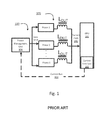
The processor includes a central processor, a graphics processor and so on. In the follow, take the graphics processor as an example to illustrate. In existing technology, a graphics processing unit (GPU) and a power management unit are two individual parts in the graphics processor. The design and the manufacture of the power management unit and those of the GPU are separated. The two parts communicate with each other through a control bus and some interfaces. FIG. 1 illustrates a processor 100 in the prior art, including a GPU 101, a power management unit 104 and an external power supply component 105. The GPU 101 sends a digital control signal for voltage from the control interface thereof to the power management unit 104 via a control bus 103 according to such as the I2C protocol and the Voltage Identification (VID) technology. The power management unit 104 sends a pulse-width modulation (PWM) signal to the external power supply component 105 according to the received digital control signal. The external power supply component 105 outputs a power supply signal according to the received PWM signal. The power supply signal was input into the GPU 101 via a current path 106. During this process, because the GPU 101 and the power management unit 104 are two individual parts, there are transients and noises in the processor 100.
Therefore, in order to solve the above-mentioned problems, there is a need of providing a processor which has much better performance and much simpler structure.
SUMMARY OF THE INVENTION
The present invention is related to a processor and a circuit board including the processor.
In one aspect of the invention, a processor is disclosed in the present invention. The processor includes a data processing unit, and an external power supply component that is coupled to the data processing unit; wherein the data processing unit includes a power management unit that is integrated into the data processing unit, and the power management unit is used for performing power management for the data processing unit; and the power management unit further includes a pulse signal output terminal which is used for outputting a pulse-width modulation signal, and the pulse-width modulation signal controls the external power supply component to supply a stable operating voltage to the data processing unit.
Preferably, the power management unit further includes a detecting terminal for receiving a signal of an operating voltage that is sampled from a core processing unit of the data processing unit; an operating status signal output terminal for outputting the signal of the operating voltage to the core processing unit to obtain a controlling signal for a duty cycle of the pulse-width modulation signal by being processed by the core processing unit; a controlling signal input terminal for receiving the controlling signal for the duty cycle from the core processing unit to control the pulse-width modulation signal.
Preferably, the detecting terminal, the operating status signal output terminal and the controlling signal input terminal are connected with the core processing unit by physical connections.
Preferably, the physical connections are copper wire connections.
Preferably, the power management unit further includes a detecting terminal for receiving a signal of an operating voltage that is sampled from a core processing unit of the data processing unit; a controller for calculating a duty cycle of the pulse-width modulation signal according to a difference value between the operating voltage and a desired operating voltage to control the pulse-width modulation signal.
Preferably, the controller also calculates the duty cycle of the pulse-width modulation signal according to a current change rate of the operating voltage.
Preferably, the pulse signal output terminal is a general-purpose input/output of the data processing unit.
Preferably, the external power supply component includes a multiphase power generation circuit.
Preferably, the multiphase power generation circuit includes driver circuits and MOSFETs.
Preferably, the processor includes a graphics processor and a central processor.
According to another aspect of the present invention, the invention is related to a circuit board, including a processor, wherein the processor includes a data processing unit, and an external power supply component that is coupled to the data processing unit; wherein the data processing unit includes a power management unit that is integrated into the data processing unit, and the power management unit is used for performing power management for the data processing unit; and the power management unit further includes a pulse signal output terminal which is used for outputting a pulse-width modulation signal, and the pulse-width modulation signal controls the external power supply component to supply a stable operating voltage to the data processing unit.
Preferably, the power management unit further includes a detecting terminal for receiving a signal of an operating voltage that is sampled from a core processing unit of the data processing unit; an operating status signal output terminal for outputting the signal of the operating voltage to the core processing unit to obtain a controlling signal for a duty cycle of the pulse-width modulation signal by being processed by the core processing unit; a controlling signal input terminal for receiving the controlling signal for the duty cycle from the core processing unit to control the pulse-width modulation signal.
Preferably, the detecting terminal, the operating status signal output terminal and the controlling signal input terminal are connected with the core processing unit by physical connections.
Preferably, the physical connections are copper wire connections.
Preferably, the power management unit further includes a detecting terminal for receiving a signal of an operating voltage that is sampled from a core processing unit of the data processing unit; a controller for calculating a duty cycle of the pulse-width modulation signal according to a difference value between the operating voltage and a desired operating voltage to control the pulse-width modulation signal.
Preferably, the controller also calculates the duty cycle of the pulse-width modulation signal according to a current change rate of the operating voltage.
Preferably, the pulse signal output terminal is a general-purpose input/output of the data processing unit.
Preferably, the external power supply component includes a multiphase power generation circuit.
Preferably, the multiphase power generation circuit includes driver circuits and MOSFETs.
Preferably, the circuit board includes a graphics card and a main board.
The performance and the stability of the processor provided by the present invention are significantly improved, and the structure of the processor is simple.
Additional features and advantages of the invention will be set forth in the description that follows, and in part will be apparent from the description, or may be learned by practice of the invention. The advantages of the invention will be realized and attained by the structure particularly pointed out in the written description and claims hereof as well as the appended drawings.
It is to be understood that both the foregoing general description and the following detailed description are exemplary and explanatory and are intended to provide further explanation of the invention as claimed.
BRIEF DESCRIPTION OF THE DRAWINGS
The accompanying drawings are included to provide a further understanding of the invention, and are incorporated in and constitute a part of this specification. The drawings illustrate embodiments of the invention and, together with the description, serve to explain the principles of the invention. In the drawings,
FIG. 1 is a schematic diagram of a processor in the prior art; and
FIG. 2 is a schematic diagram of a processor according to a preferred embodiment of the present invention.
DETAILED DESCRIPTION
Example embodiments are described herein in the context of a processor and a circuit board including the processor. Those of ordinary skill in the art will realize that the following description is illustrative only and is not intended to be in any way limiting. Other embodiments will readily suggest themselves to those skilled in the art having the benefit of this disclosure. Reference will now be made in detail to implementations of the example embodiments as illustrated in the accompanying drawings. The same reference numbers will be used to the extent possible throughout the drawings and the following description to refer to the same or like items.
The present invention is related to a processor. The ordinary skilled in the art could understand that the processor may include a central processor and a graphics processor.
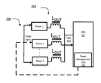
In the following, take a graphics processor as an example to describe the processor in detail. FIG. 2 shows a schematic diagram of a graphics processor 200 according to a preferred embodiment of the present invention. The graphics processor 200 includes a data processing unit 201 and an external power supply component 203 that is coupled to the data processing unit 201. In the exemplary embodiment, the data processing unit is a GPU. The GPU 201 includes a power management unit 202 that is integrated into the GPU 201, and the power management unit 202 is used for performing power management for the GPU 201. The power management unit 202 further includes a pulse signal output terminal which is used for outputting a PWM signal, and the PWM signal controls the external power supply component 203 to supply a stable operating voltage to the GPU 201.
In the exemplary embodiment, the power management unit 202 is integrated into the GPU 201 of the graphics processor 200, which avoids the requirement for a communication bus between the GPU and the power management unit 202 and reduces the complexity of a circuit board. Meanwhile, on one hand, an external sensitive signal of a chip is not produced, and in turn the risk of system failure is decreased; on the other hand, the control signal is not delayed, the reason of all of which is that the power management unit 202 communicates with other units of the GPU 201 in the GPU 201.
An external power supply of the GPU 201 supplies power to the power management unit 202 that is integrated into the GPU 201, and the power management unit 202 generates the PWM signal according to the operating voltage required by the GPU 201. The PWM signal output terminal of the power management unit 202 outputs the PWM signal to supply to the GPU 201 via the external power supply component 203.
According to one exemplary embodiment of the present invention, the power management unit 202 may further include a detecting terminal, an operating status signal output terminal and a controlling signal input terminal. The detecting terminal for receiving a signal of an operating voltage that is sampled from a core processing unit of the GPU 201. The operating status signal output terminal for outputting the signal of the operating voltage to the core processing unit to obtain a controlling signal for a duty cycle of the PWM signal by being processed by the core processing unit. A controlling signal input terminal for receiving the controlling signal for the duty cycle from the core processing unit to control the PWM signal.
The ordinary skilled in the art could understand that the detecting terminal, the operating status signal output terminal and the controlling signal input terminal mentioned above may be merged into one terminal. Preferably, the detecting terminal, the operating status signal output terminal and the controlling signal input terminal can be connected with the core processing unit by physical connections. The ordinary skilled in the art could understand that the detecting terminal, the operating status signal output terminal and the controlling signal input terminal could also be connected with the core processing unit by high-speed bus connections. Both the power management unit 202 and the core processing unit are located in the GPU 201, and the distance between these two is small. The low-cost internal physical connections can satisfy the connection between the power management unit 202 and the core processing unit because the electrical signals between these are simple. The high-speed bus connections could avoid additional wiring, but there is various complex data transmitted via the high-speed bus connections. So an unexpected error may be produced if the detecting terminal, the operating status signal output terminal and the controlling signal input terminal are connected with the core processing unit by the high-speed bus connections. The ordinary skilled in the art could understand that the above-mentioned physical connections may be copper wire connections, which could not only save cost but also satisfy the requirement. The connections certainly may be other mental wire connections, for example platinum wire connections, aluminum wire connections, etc.
The power management unit 202 determines current operating status of the GPU 201 by sampling the operating voltage of the core processing unit. And the power management unit 202 receives the signal of the operating voltage that is sampled from the core processing unit of the GPU 201 via the detecting terminal. Then the signal of the operating voltage is output to the core processing unit. The controlling signal for a duty cycle of the PWM signal to be output is calculated by the core processing unit. And then the power management unit 202 receives the controlling signal for the duty cycle from the core processing unit via the controlling signal input terminal. The power management unit 202 controls the PWM signal to be output according to the received controlling signal for the duty cycle.
When the load of the GPU 201 gets larger, the operating voltage of the core processing unit is decreased. At this time, the power management unit 202 receives the controlling signal for the duty cycle which makes the duty cycle of the PWM signal get larger. Finally, the power management unit 202 outputs the PWM signal with the larger duty cycle to the GPU 201 via the external power supply component to satisfy the requirement of the load of the GPU 201.
As known to all, the GPU 201 has a powerful calculating capability, which may calculate the required operating voltage according to the current load condition of the core processing unit to achieve well power controlling. A transfer function for controlling which is very complex and even unable to be achieved by an existing the power management unit may be very easy for a GPU. In the exemplary embodiment, the power management unit 202 could effectively power management by using the GPU 201, because the power management unit 202 is located in the GPU 201.
According to another exemplary embodiment of the present invention, the power management unit 202 may further include a detecting terminal and a controller. The detecting terminal is used for receiving a signal of an operating voltage that is sampled from a core processing unit of the GPU 201. The controller for calculating a duty cycle of the PWM signal according to a difference value between the operating voltage and a desired operating voltage to control the PWM signal.
Similar with the previous exemplary embodiment, the power management unit 202 receives the signal of the operating voltage that is sampled from the core processing unit of the GPU 201 via the detecting terminal. The controller of the power management unit 202 calculates a difference value between the operating voltage and the desired operating voltage, and controls the duty cycle of the PWM signal according to the different value. For example, if the desired operating voltage of the core processing unit is higher than the sampled actual operating voltage, the controller determines a higher duty cycle. The power management unit 202 outputs the PWM signal with the higher duty cycle determined by the controller to the GPU 201.
Preferably, the controller of the power management unit 202 also calculates the duty cycle of the PWM signal according to a current change rate of the operating voltage. The power management unit 202 obtains the current change rate of the operating voltage of the core processing unit by sampling the operating voltage of the core processing unit during a period. The controller calculates the duty cycle of the PWM signal according to a current change rate of the operating voltage to control the PWM signal.
For example, the power management unit 202 samples the operating voltage of the core processing unit during 1 microsecond and is known that the current change rate of the operating voltage of the core processing unit gets smaller during this period. Therefore, the controller could forecasts that the load change of the GPU 201 is decreased according to the current change rate of the operating voltage. So the operating voltage of the core processing unit could not be changed very quickly, and the adjusting speed of the duty cycle of the PWM signal could be slowed down. In this way, over modulation could be avoided, and then the stability of the graphics processor may be improved and the power management may be more accurate.
The pulse signal output terminal of the power management unit 202 may be a general-purpose input/output (GPIO) of the GPU 201. The GPIO is an existing interface on the processor, which may be programmable. In an exemplary embodiment of the present invention, the power management unit 202 outputs a PWM signal via a GPIO instead of a special interface, which simplifies the design of the processor.
The external power supply component may include a multiphase power generation circuit. The multiphase power generation circuit may include multiple BUCK circuits in parallel. Each BUCK circuit receives a PWM signal. The multiphase power generation circuit outputs a voltage required by the GPU 201. Wherein the phase number of the multiphase power generation circuit depends on a full-load current of the GPU 201. If one phase of the multiphase power generation circuit may support a 25 A current, the phase number of the multiphase power generation circuit is a ratio of the amperage of the full-load current of the GPU 201 to 25 A. For example, provided that the full-load current of the GPU 201 is about 75 A, the phase number of the multiphase power generation circuit is 3.
In present exemplary embodiment, the structure of the external power supply component may be very simple. Preferably, each BUCK circuit of the multiple BUCK circuits may include driver circuits and MOSFETs. The MOSFETs may be integrated.
According to another aspect of the present invention, a circuit board is disclosed. The circuit board includes the above-mentioned processor. For brevity, a detailed description is omitted for the processor described with reference to the above embodiments. Those skilled in the art can understand that the specific structure and the operation mode of the processor with reference to FIG. 2 in combination with the above description.
In the circuit board, the power management unit is integrated into the data processing unit. The complexity of the wiring is reduced. Meanwhile, the controlling delay in the power management process is reduced and the transient performance of the circuit board is improved, because all the communication between the power management unit and the other units of the data processing unit is in the data processing unit.
The circuit board may be any circuit board that comprises the above-mentioned processor. Optionally, the circuit board includes a graphics card and a main board.
It should be appreciated that various modifications, adaptations and alternative embodiments thereof may be made within the scope and spirit of the present invention. The invention is further defined by the following claims.

Claims (25)

The invention claimed is:
1. A processor, including:
a data processing unit comprising a power management unit and a core processing unit and configured to calculate a first operating voltage associated with operating the core processing unit based on a transfer function and on a first load condition associated with the core processing unit, wherein the power management unit is configured to:
calculate a first difference value between the first operating voltage and a desired operating voltage for operating the core processing unit, and
calculate a first duty cycle of a pulse-width modulated signal based on the first difference value,
wherein the data processing unit is configured to output the pulse-width modulated signal having the first duty cycle; and
an external power supply component that is coupled to the data processing unit and configured to receive the pulse-width modulated signal having the first duty cycle from the data processing unit and to supply a modified first operating voltage associated with operating the core processing unit based on the pulse-width modulated signal having the first duty cycle.
2. The processor of claim 1, wherein the power management unit further includes:
a detecting terminal for receiving a signal of the first operating voltage that is sampled from the core processing unit of the data processing unit;
an operating status signal output terminal for outputting the signal of the first operating voltage to the core processing unit to obtain a controlling signal for a duty cycle of the pulse-width modulation signal by being processed by the core processing unit;
a controlling signal input terminal for receiving the controlling signal for the duty cycle from the core processing unit to control the pulse-width modulation signal.
3. The processor of claim 2, wherein the detecting terminal, the operating status signal output terminal and the controlling signal input terminal are connected with the core processing unit by physical connections.
4. The processor of claim 3, wherein the physical connections are copper wire connections.
5. The processor of claim 1, wherein the power management unit further includes:
a detecting terminal for receiving a signal of the first operating voltage that is sampled from the core processing unit of the data processing unit; and
a controller for calculating the first duty cycle of the pulse-width modulation signal according to a difference value between the first operating voltage and the desired operating voltage to control the pulse-width modulation signal.
6. The processor of claim 1, wherein the power management unit also calculates the first duty cycle of the pulse-width modulation signal according to a current rate at which the first operating voltage is changing.
7. The processor of claim 1, wherein the power management unit includes a pulse signal output terminal that is a general-purpose input output of the data processing unit.
8. The processor of claim 1, wherein the external power supply component includes a multiphase power generation circuit.
9. The processor of claim 8, wherein the multiphase power generation circuit includes driver circuits and MOSFETs (metal-oxide-semiconductor field effect transistors).
10. The processor of claim 1, wherein the processor includes a graphics processor and a central processor.
11. The processor of claim 1, wherein the power management unit is further configured to:
calculate a second difference value between a second operating voltage and the desired operating voltage, wherein the second difference is greater than the first difference, and
calculate a second duty cycle of the pulse-width modulated signal based on the second difference value, wherein the second duty cycle is greater than the first duty cycle.
12. The processor of claim 1, wherein the first duty cycle is further based on a first rate at which the first operating voltage is changing.
13. The processor of claim 12, wherein the power management unit is further configured to:
determine a second change rate associated with the first operating voltage, wherein the second change rate is less than the first change rate, and
calculate a third difference value between the first change rate and the second change rate, and
calculate a third duty cycle of the pulse-width modulated signal based on the third difference value, wherein the third duty cycle is less than the first duty cycle.
14. A circuit board, including:
a processor, wherein the processor includes:
a data processing unit comprising a power management unit and a core processing unit and configured to calculate a first operating voltage associated with operating the core processing unit based on a function and on a first load condition associated with the core processing unit, wherein the power management unit is configured to:
calculate a first difference value between the first operating voltage and a desired operating voltage for operating the core processing unit, and
calculate a first duty cycle of a pulse-width modulated signal based on the first difference value,
wherein the data processing unit is configured to output the pulse-width modulated signal having the first duty cycle; and
an external power supply component that is coupled to the data processing unit and configured to receive the pulse-width modulated signal having the first duty cycle from the data processing unit and to supply a modified first operating voltage associated with operating the core processing unit based on the pulse-width modulated signal having the first duty cycle.
15. The circuit board of claim 14, wherein the power management unit further includes:
a detecting terminal for receiving a signal of the first operating voltage that is sampled from the core processing unit of the data processing unit;
an operating status signal output terminal for outputting the signal of the first operating voltage to the core processing unit to obtain a controlling signal for a duty cycle of the pulse-width modulation signal by being processed by the core processing unit;
a controlling signal input terminal for receiving the controlling signal for the duty cycle from the core processing unit to control the pulse-width modulation signal.
16. The circuit board of claim 15, wherein the detecting terminal, the operating status signal output terminal and the controlling signal input terminal are connected with the core processing unit by physical connections.
17. The circuit board of claim 16, wherein the physical connections are copper wire connections.
18. The circuit board of claim 14, wherein the power management unit further includes:
a detecting terminal for receiving a signal of the first operating voltage that is sampled from the core processing unit of the data processing unit;
a controller for calculating the duty cycle of the pulse-width modulation signal according to a difference value between the first operating voltage and a desired operating voltage to control the pulse-width modulation signal.
19. The circuit board of claim 14, wherein the power management unit also calculates the first duty cycle of the pulse-width modulation signal according to a current rate at which the first operating voltage is changing.
20. The circuit board of claim 14, wherein the power management unit includes a pulse signal output terminal that is a general-purpose input /output of the data processing unit.
21. The circuit board of claim 14, wherein the external power supply component includes a multiphase power generation circuit.
22. The circuit board of claim 21, wherein the multiphase power generation circuit includes driver circuits and MOSFETs (metal-oxide-semiconductor field effect transistors).
23. The circuit board of claim 14, wherein the circuit board includes a graphics card and a main board.
24. A processor, comprising:
a data processing unit comprising a power management unit and a core processing unit and configured to calculate a first operating voltage associated with operating the core processing unit based on a transfer function and on a first load condition associated with the core processing unit, wherein the power management unit is configured to:
calculate a first difference value between the first operating voltage and a desired operating voltage for operating the core processing unit, and
calculate a first duty cycle of a pulse-width modulated signal based on the first difference value and according to a current rate at which the first operating voltage is changing; and
an external power supply component that is coupled to the data processing unit and configured to supply a modified first operating voltage associated with operating the core processing unit based on the pulse-width modulated signal.
25. A circuit board, including:
a processor, wherein the processor includes:
a data processing unit comprising a power management unit and a core processing unit and configured to calculate a first operating voltage associated with operating the core processing unit based on a function and on a first load condition associated with the core processing unit, wherein the power management unit is configured to:
calculate a first difference value between the first operating voltage and a desired operating voltage for operating the core processing unit, and
calculate a first duty cycle of a pulse-width modulated signal based on the first difference value and according to a current rate at which the first operating voltage is changing; and
an external power supply component that is coupled to the data processing unit and configured to supply a modified first operating voltage associated with operating the core processing unit based on the pulse-width modulated signal.
US13/791,322 2012-11-09 2013-03-08 Processor and circuit board including a power management unit Active 2034-09-06 US9817455B2 (en)

Priority Applications (2)

Application Number Priority Date Filing Date Title
DE102013018384.7A DE102013018384B4 (en) 2012-11-09 2013-11-04 Processor and circuit board with the processor
TW102140310A TWI626533B (en) 2012-11-09 2013-11-06 Processor and circuit board including the processor

Applications Claiming Priority (3)

Application Number Priority Date Filing Date Title
CN201210449269.9A CN103810141A (en) 2012-11-09 2012-11-09 Processor and circuit board comprising same
CN201210449269 2012-11-09
CN201210449269.9 2012-11-09

Publications (2)

Publication Number Publication Date
US20140136862A1 US20140136862A1 (en) 2014-05-15
US9817455B2 true US9817455B2 (en) 2017-11-14

Family

ID=50682908

Family Applications (1)

Application Number Title Priority Date Filing Date
US13/791,322 Active 2034-09-06 US9817455B2 (en) 2012-11-09 2013-03-08 Processor and circuit board including a power management unit

Country Status (4)

Country Link
US (1) US9817455B2 (en)
CN (1) CN103810141A (en)
DE (1) DE102013018384B4 (en)
TW (1) TWI626533B (en)

Families Citing this family (1)

* Cited by examiner, † Cited by third party
Publication number Priority date Publication date Assignee Title
US11137815B2 (en) 2018-03-15 2021-10-05 Nvidia Corporation Metering GPU workload with real time feedback to maintain power consumption below a predetermined power budget

Citations (20)

* Cited by examiner, † Cited by third party
Publication number Priority date Publication date Assignee Title
US20060026447A1 (en) * 2004-07-27 2006-02-02 Intel Corporation Power management coordination in multi-core processors
US20070033425A1 (en) * 2005-08-02 2007-02-08 Advanced Micro Devices, Inc. Increasing workload performance of one or more cores on multiple core processors
US20070174586A1 (en) * 2005-04-15 2007-07-26 Rambus, Inc. Processor controlled interface
TW200928702A (en) 2007-12-18 2009-07-01 Inventec Corp Power management module for central processing unit
US20090224732A1 (en) * 2008-03-07 2009-09-10 Ryotaro Kudo Power supply unit
US20090300377A1 (en) * 2008-05-29 2009-12-03 Kuo-Chung Kao Computer system for Managing Power consumption and Method Thereof
US20100130139A1 (en) * 2008-11-25 2010-05-27 Qualcomm Incorporated Duty cycle adjustment for a local oscillator signal
US20100188126A1 (en) * 2009-01-26 2010-07-29 International Business Machines Corporation Voltage Controlled Duty Cycle and Non-Overlapping Clock Generation Implementation
US20110264938A1 (en) * 2011-06-30 2011-10-27 Henroid Andrew D Method and system for determining an energy-efficient operating point of a platform
US20110265090A1 (en) * 2010-04-22 2011-10-27 Moyer William C Multiple core data processor with usage monitoring
US20120066535A1 (en) * 2010-09-14 2012-03-15 Naffziger Samuel D Mechanism for controlling power consumption in a processing node
US20120086416A1 (en) * 2010-10-06 2012-04-12 Renesas Electronics Corporation Power supply device
US20120110352A1 (en) * 2010-10-29 2012-05-03 Alexander Branover Method and apparatus for thermal control of processing nodes
US20120117402A1 (en) * 2010-11-04 2012-05-10 Machnicki Erik P Memory Read Timing Margin Adjustment
US8316256B2 (en) * 2009-12-10 2012-11-20 Nvidia Corporation Method and system for supplying output voltage to graphics processing unit
US20120297232A1 (en) * 2011-05-16 2012-11-22 Bircher William L Adjusting the clock frequency of a processing unit in real-time based on a frequency sensitivity value
US20130057190A1 (en) * 2011-07-05 2013-03-07 Jens Brennenstuhl Device and method for regulating an increase in the output torque over time of an electric drive motor
US20140082377A1 (en) * 2012-09-14 2014-03-20 James S. Dinh Providing Additional Current Capacity To A Processor For A Turbo Mode
US20140089699A1 (en) * 2012-09-27 2014-03-27 Advanced Micro Devices Power management system and method for a processor
US9584302B2 (en) * 2015-06-05 2017-02-28 Analog Devices Global Method and apparatus for synchronization of slave clock to master clock

Family Cites Families (2)

* Cited by examiner, † Cited by third party
Publication number Priority date Publication date Assignee Title
US7376182B2 (en) * 2004-08-23 2008-05-20 Microchip Technology Incorporated Digital processor with pulse width modulation module having dynamically adjustable phase offset capability, high speed operation and simultaneous update of multiple pulse width modulation duty cycle registers
CN102289274A (en) * 2010-06-18 2011-12-21 鸿富锦精密工业(深圳)有限公司 CPU (Central Processing Unit) power supplying circuit

Patent Citations (20)

* Cited by examiner, † Cited by third party
Publication number Priority date Publication date Assignee Title
US20060026447A1 (en) * 2004-07-27 2006-02-02 Intel Corporation Power management coordination in multi-core processors
US20070174586A1 (en) * 2005-04-15 2007-07-26 Rambus, Inc. Processor controlled interface
US20070033425A1 (en) * 2005-08-02 2007-02-08 Advanced Micro Devices, Inc. Increasing workload performance of one or more cores on multiple core processors
TW200928702A (en) 2007-12-18 2009-07-01 Inventec Corp Power management module for central processing unit
US20090224732A1 (en) * 2008-03-07 2009-09-10 Ryotaro Kudo Power supply unit
US20090300377A1 (en) * 2008-05-29 2009-12-03 Kuo-Chung Kao Computer system for Managing Power consumption and Method Thereof
US20100130139A1 (en) * 2008-11-25 2010-05-27 Qualcomm Incorporated Duty cycle adjustment for a local oscillator signal
US20100188126A1 (en) * 2009-01-26 2010-07-29 International Business Machines Corporation Voltage Controlled Duty Cycle and Non-Overlapping Clock Generation Implementation
US8316256B2 (en) * 2009-12-10 2012-11-20 Nvidia Corporation Method and system for supplying output voltage to graphics processing unit
US20110265090A1 (en) * 2010-04-22 2011-10-27 Moyer William C Multiple core data processor with usage monitoring
US20120066535A1 (en) * 2010-09-14 2012-03-15 Naffziger Samuel D Mechanism for controlling power consumption in a processing node
US20120086416A1 (en) * 2010-10-06 2012-04-12 Renesas Electronics Corporation Power supply device
US20120110352A1 (en) * 2010-10-29 2012-05-03 Alexander Branover Method and apparatus for thermal control of processing nodes
US20120117402A1 (en) * 2010-11-04 2012-05-10 Machnicki Erik P Memory Read Timing Margin Adjustment
US20120297232A1 (en) * 2011-05-16 2012-11-22 Bircher William L Adjusting the clock frequency of a processing unit in real-time based on a frequency sensitivity value
US20110264938A1 (en) * 2011-06-30 2011-10-27 Henroid Andrew D Method and system for determining an energy-efficient operating point of a platform
US20130057190A1 (en) * 2011-07-05 2013-03-07 Jens Brennenstuhl Device and method for regulating an increase in the output torque over time of an electric drive motor
US20140082377A1 (en) * 2012-09-14 2014-03-20 James S. Dinh Providing Additional Current Capacity To A Processor For A Turbo Mode
US20140089699A1 (en) * 2012-09-27 2014-03-27 Advanced Micro Devices Power management system and method for a processor
US9584302B2 (en) * 2015-06-05 2017-02-28 Analog Devices Global Method and apparatus for synchronization of slave clock to master clock

Also Published As

Publication number Publication date
TW201432428A (en) 2014-08-16
US20140136862A1 (en) 2014-05-15
DE102013018384A1 (en) 2014-05-15
DE102013018384B4 (en) 2016-03-24
TWI626533B (en) 2018-06-11
CN103810141A (en) 2014-05-21

Similar Documents

Publication Publication Date Title
CN110649694B (en) NCSI network card power supply system
US9429973B2 (en) Power control system with performance monitoring
TW202107810A (en) Sequence assignment method used in multiphase switching converters with daisy chain configuration
EP1612910A1 (en) On-board power supply monitor and power control system
CN101931321B (en) Power conversion circuit
US10073509B2 (en) Electronic device for combining multiple power signals
KR101727219B1 (en) High-frequency on-package voltage regulator
US9484920B2 (en) Switching circuit and electronic device
CN102195461A (en) DC-DC soft starting control circuit
US7990200B2 (en) Pulse width modulation control system
US9817455B2 (en) Processor and circuit board including a power management unit
WO2024087418A1 (en) Multi-voltage independent output circuit of single-inductor transformer and related product
US11309814B2 (en) Electric motor power control circuitry
CN103092304A (en) Power supply control method of double display card module and computer device applying same
US20130187463A1 (en) Switching Power Control Device and Control Method of the Same
US9436243B2 (en) Circuit board and power source management system of circuit board
US20130124880A1 (en) Power supply device for central processing unit
US20140132243A1 (en) Two-wire transmitter starter circuit and two-wire transmitter including the same
CN203149564U (en) Serial-port automatic switching device
CN107908269A (en) A kind of more POL parallel combinations electric power systems and method of supplying power to
US20110115459A1 (en) Phase adjusting system and method
CN100517929C (en) Multi-phase DC-DC power converter with expansion circuit
CN112034414A (en) A kind of self-adaptive sampling method, system and equipment of electric meter core board
CN202917395U (en) Electromagnetic relay control device with power supply enable module
JP4649490B2 (en) Power management method and system for main board

Legal Events

Date Code Title Description
AS Assignment

Owner name: NVIDIA CORPORATION, CALIFORNIA

Free format text: ASSIGNMENT OF ASSIGNORS INTEREST;ASSIGNOR:ZHAO, YU;REEL/FRAME:029955/0524

Effective date: 20130308

STCF Information on status: patent grant

Free format text: PATENTED CASE

MAFP Maintenance fee payment

Free format text: PAYMENT OF MAINTENANCE FEE, 4TH YEAR, LARGE ENTITY (ORIGINAL EVENT CODE: M1551); ENTITY STATUS OF PATENT OWNER: LARGE ENTITY

Year of fee payment: 4

MAFP Maintenance fee payment

Free format text: PAYMENT OF MAINTENANCE FEE, 8TH YEAR, LARGE ENTITY (ORIGINAL EVENT CODE: M1552); ENTITY STATUS OF PATENT OWNER: LARGE ENTITY

Year of fee payment: 8