US9817426B2 - Low quiescent current voltage regulator with high load-current capability - Google Patents

Low quiescent current voltage regulator with high load-current capability Download PDF

Info

Publication number
US9817426B2
US9817426B2 US14/533,555 US201414533555A US9817426B2 US 9817426 B2 US9817426 B2 US 9817426B2 US 201414533555 A US201414533555 A US 201414533555A US 9817426 B2 US9817426 B2 US 9817426B2
Authority
US
United States
Prior art keywords
voltage
current mirror
voltage regulator
terminal
transistor
Prior art date
Legal status (The legal status is an assumption and is not a legal conclusion. Google has not performed a legal analysis and makes no representation as to the accuracy of the status listed.)
Active, expires
Application number
US14/533,555
Other versions
US20160124454A1 (en
Inventor
Ananthasayanam Chellappa
Current Assignee (The listed assignees may be inaccurate. Google has not performed a legal analysis and makes no representation or warranty as to the accuracy of the list.)
NXP BV
Original Assignee
NXP BV
Priority date (The priority date is an assumption and is not a legal conclusion. Google has not performed a legal analysis and makes no representation as to the accuracy of the date listed.)
Filing date
Publication date
Application filed by NXP BV filed Critical NXP BV
Priority to US14/533,555 priority Critical patent/US9817426B2/en
Assigned to NXP B.V. reassignment NXP B.V. ASSIGNMENT OF ASSIGNORS INTEREST (SEE DOCUMENT FOR DETAILS). Assignors: CHELLAPPA, ANANTHASAYANAM
Priority to EP15187595.2A priority patent/EP3018551A1/en
Priority to CN201510726136.5A priority patent/CN105573394B/en
Publication of US20160124454A1 publication Critical patent/US20160124454A1/en
Application granted granted Critical
Publication of US9817426B2 publication Critical patent/US9817426B2/en
Active legal-status Critical Current
Adjusted expiration legal-status Critical

Links

Images

Classifications

    • GPHYSICS
    • G05CONTROLLING; REGULATING
    • G05FSYSTEMS FOR REGULATING ELECTRIC OR MAGNETIC VARIABLES
    • G05F3/00Non-retroactive systems for regulating electric variables by using an uncontrolled element, or an uncontrolled combination of elements, such element or such combination having self-regulating properties
    • G05F3/02Regulating voltage or current
    • G05F3/08Regulating voltage or current wherein the variable is DC
    • G05F3/10Regulating voltage or current wherein the variable is DC using uncontrolled devices with non-linear characteristics
    • G05F3/16Regulating voltage or current wherein the variable is DC using uncontrolled devices with non-linear characteristics being semiconductor devices
    • G05F3/20Regulating voltage or current wherein the variable is DC using uncontrolled devices with non-linear characteristics being semiconductor devices using diode- transistor combinations
    • G05F3/26Current mirrors
    • G05F3/262Current mirrors using field-effect transistors only
    • GPHYSICS
    • G05CONTROLLING; REGULATING
    • G05FSYSTEMS FOR REGULATING ELECTRIC OR MAGNETIC VARIABLES
    • G05F1/00Automatic systems in which deviations of an electric quantity from one or more predetermined values are detected at the output of the system and fed back to a device within the system to restore the detected quantity to its predetermined value or values, i.e. retroactive systems
    • G05F1/10Regulating voltage or current 
    • G05F1/46Regulating voltage or current  wherein the variable actually regulated by the final control device is DC
    • G05F1/56Regulating voltage or current  wherein the variable actually regulated by the final control device is DC using semiconductor devices in series with the load as final control devices
    • GPHYSICS
    • G05CONTROLLING; REGULATING
    • G05FSYSTEMS FOR REGULATING ELECTRIC OR MAGNETIC VARIABLES
    • G05F3/00Non-retroactive systems for regulating electric variables by using an uncontrolled element, or an uncontrolled combination of elements, such element or such combination having self-regulating properties
    • G05F3/02Regulating voltage or current
    • G05F3/08Regulating voltage or current wherein the variable is DC
    • G05F3/10Regulating voltage or current wherein the variable is DC using uncontrolled devices with non-linear characteristics
    • G05F3/16Regulating voltage or current wherein the variable is DC using uncontrolled devices with non-linear characteristics being semiconductor devices
    • G05F3/20Regulating voltage or current wherein the variable is DC using uncontrolled devices with non-linear characteristics being semiconductor devices using diode- transistor combinations
    • G05F3/24Regulating voltage or current wherein the variable is DC using uncontrolled devices with non-linear characteristics being semiconductor devices using diode- transistor combinations wherein the transistors are of the field-effect type only
    • G05F3/242Regulating voltage or current wherein the variable is DC using uncontrolled devices with non-linear characteristics being semiconductor devices using diode- transistor combinations wherein the transistors are of the field-effect type only with compensation for device parameters, e.g. channel width modulation, threshold voltage, processing, or external variations, e.g. temperature, loading, supply voltage
    • GPHYSICS
    • G05CONTROLLING; REGULATING
    • G05FSYSTEMS FOR REGULATING ELECTRIC OR MAGNETIC VARIABLES
    • G05F3/00Non-retroactive systems for regulating electric variables by using an uncontrolled element, or an uncontrolled combination of elements, such element or such combination having self-regulating properties
    • G05F3/02Regulating voltage or current
    • G05F3/08Regulating voltage or current wherein the variable is DC
    • G05F3/10Regulating voltage or current wherein the variable is DC using uncontrolled devices with non-linear characteristics
    • G05F3/16Regulating voltage or current wherein the variable is DC using uncontrolled devices with non-linear characteristics being semiconductor devices
    • G05F3/20Regulating voltage or current wherein the variable is DC using uncontrolled devices with non-linear characteristics being semiconductor devices using diode- transistor combinations
    • G05F3/26Current mirrors

Definitions

  • a voltage regulator converts an input voltage into an output voltage and can be used to provide a stable operating voltage to components of an integrated circuit (IC). For example, some integrated circuits use a low-dropout (LDO) regulator to convert a 3.3 volt (V) voltage rail into a 1.8V voltage rail for digital logic cells. Because an LDO regulator is a feedback voltage regulator, the output voltage of the LDO regulator is well-regulated. However, to make an LDO regulator stable across a range of output capacitances and load-currents, the quiescent/standby current of the LDO regulator, which is the current drawn internally within the LDO regulator, is on the order of tens of microamperes. However, a large quiescent current results in high power consumption during operation in a standby mode.
  • LDO low-dropout
  • a voltage regulator includes a set of current mirror circuits configured to convert an input voltage into an output voltage and a voltage buffer circuit configured to buffer a reference voltage for the set of current mirror circuits.
  • the set of current mirror circuits form a positive feedback loop.
  • the voltage regulator uses the positive feedback loop that is formed by the current mirror circuits for voltage conversion. Consequently, compared to a conventional voltage regulator, the voltage regulator can have a low quiescent or standby current and low power consumption during operation in a standby mode.
  • Other embodiments are also described.
  • a voltage regulator includes a set of current mirror circuits configured to convert an input voltage into an output voltage and a voltage buffer circuit configured to buffer a reference voltage for the set of current mirror circuits.
  • the set of current mirror circuits form a positive feedback loop.
  • a voltage regulator includes a set of current mirror circuits configured to convert an input direct current (DC) voltage into an output DC voltage and a voltage buffer circuit configured to buffer a reference DC voltage for the set of current mirror circuits.
  • the set of current mirror circuits form a positive feedback loop having a loop gain that is less than 1, and the output voltage is lower than the input voltage.
  • a method for operating a voltage regulator involves buffering a reference voltage for a set of current mirror circuits and converting an input voltage into an output voltage using the set of current mirror circuits.
  • the set of current mirror circuits form a positive feedback loop.
  • FIG. 1 is a schematic block diagram of a voltage regulator in accordance with an embodiment of the invention.
  • FIG. 2 depicts an embodiment of the voltage regulator depicted in FIG. 1 .
  • FIG. 3 depicts an embodiment of a pin configuration of a packaged IC device.
  • FIG. 4 is a process flow diagram of a method for operating a voltage regulator in accordance with an embodiment of the invention.
  • FIG. 1 is a schematic block diagram of a voltage regulator 100 in accordance with an embodiment of the invention.
  • the voltage regulator 100 includes two current mirror circuits 102 - 1 , 102 - 2 and a voltage buffer circuit 104 .
  • the voltage regulator converts an input voltage into an output voltage.
  • the input and output voltages can be any suitable type of voltages. In some embodiments, the input and output voltages are direct current (DC) voltages.
  • the voltage regulator can be used to provide an operating voltage for components of an IC.
  • the voltage regulator converts an input voltage of around (e.g., ⁇ 30%) 3.3 Volts (V) into an output voltage of around (e.g., ⁇ 30%) 1.8V, and in other embodiments, the voltage regulator converts an input voltage of around 5V into an output voltage of around 1.5V.
  • the input and output voltages of the voltage regulator are not limited by the example voltages.
  • the voltage regulator is shown in FIG. 1 as including certain components, in some embodiments, the voltage regulator includes less or more components to implement less or more functionalities.
  • the voltage regulator includes a startup circuit used to generate a startup current.
  • the current mirror circuits 102 - 1 , 102 - 2 of the voltage regulator 100 are configured to convert an input voltage into an output voltage.
  • the output voltage of the voltage regulator may be lower than the reference voltage of the voltage regulator or higher than the reference voltage of the voltage regulator.
  • the current mirror circuits form the positive feedback loop 106 .
  • an input terminal, “IN,” of the current mirror circuit 102 - 1 is connected to an output terminal, “OUT,” of the current mirror circuit 102 - 2 and an output terminal, “OUT,” of the current mirror circuit 102 - 1 is connected to an input terminal, “IN,” of the current mirror circuit 102 - 2 .
  • a positive feedback loop is a feedback loop having a positive loop gain.
  • the feedback is in phase with the input of the feedback loop such that an increase at the input causes a change in the feedback, which in turn causes a larger increase at the input.
  • the voltage regulator can be started from a low-power standby mode based on a small quiescent or standby current.
  • the quiescent current in the voltage regulator is the current drawn internally within the voltage regulator.
  • the quiescent current in the voltage regulator is measured as the input current while no load is connected to the voltage regulator.
  • the positive feedback loop 106 has a loop gain that is greater than zero but less than 1. Generally, if the loop gain of a feedback loop is greater than 1, the feedback loop can have exponential growth, which causes the feedback loop to be unstable.
  • the voltage buffer circuit 104 of the voltage regulator 100 is configured to buffer a reference voltage for the current mirror circuits 102 - 1 , 102 - 2 .
  • the reference voltage is generally lower than the input voltage of the voltage regulator.
  • the reference voltage can be about (e.g., ⁇ 30%) half of the input voltage of the voltage regulator.
  • the voltage buffer circuit is used to transfer a voltage from a first circuit (e.g., a reference generation circuit that generates the reference voltage), having a high output impedance, to a second circuit (e.g., the current mirror circuit 102 - 2 ) with a low input impedance.
  • the voltage buffer circuit can prevent a circuit at its input from interfering with the desired operation of a circuit at its output.
  • the voltage buffer circuit includes a source follower circuit.
  • ICs generally use a voltage regulator circuit that achieves good output voltage regulation in the presence of large load-current variation.
  • a low-dropout (LDO) regulator is used in an IC to convert an input voltage into a suitable operating voltage for IC components.
  • LDO low-dropout
  • a certain minimum quiescent current is needed to ensure that the unity gain frequency (UGF) of the LDO regulator is above a certain threshold or to ensure that non-dominant pole-frequencies of the LDO regulator are in an acceptable range.
  • ULF unity gain frequency
  • the voltage regulator uses the positive feedback loop 106 that is formed by the current mirror circuits 102 - 1 , 102 - 2 for voltage conversion. Because the current mirror circuits, which form the positive feedback loop, can be simply implemented, the voltage regulator can be implemented using a simplified circuit structure. Consequently, compared to a conventional voltage regulator, the voltage regulator can have a low quiescent or standby current. For example, the voltage regulator can have a quiescent current that is equal to or below 1 microampere ( ⁇ A).
  • the positive feedback loop formed by the current mirror circuits in general is stable when the loop gain is less than 1. Consequently, the output voltage of the voltage regulator can be reasonably well-regulated.
  • FIG. 2 depicts an embodiment of the voltage regulator 100 of FIG. 1 .
  • a DC voltage regulator 200 includes a startup circuit 210 , two current mirror circuits 202 - 1 , 202 - 2 that form a positive loop 206 , a voltage buffer circuit 204 , and a resistor 212 .
  • the voltage regulator 200 depicted in FIG. 2 is one possible embodiment of the voltage regulator 100 depicted in FIG. 1 .
  • the voltage regulator depicted in FIG. 1 is not limited to the embodiment shown in FIG. 2 .
  • the voltage regulator 200 can have low standby power consumption, high load-current capability, and a reasonable output-voltage compliance range.
  • the voltage regulator can have a quiescent current on the order of 1 ⁇ A while supporting a load in the range of several hundred microamperes. Consequently, the voltage regulator can provide sufficient processing power to detect the need to exit a low-power mode and to enable a full-fledged LDO.
  • the output voltage of the voltage regulator may not be well regulated (e.g., the output voltage can be low for a low load) and the voltage regulator may not be a low-dropout solution (e.g., the input voltage may be higher than 2.9V), the voltage regulator can be used to replace an LDO in a low-power-mode.
  • the voltage regulator 200 converts an input voltage, “VDD 3 V 3 ,” into an output voltage, “VDD 1 V 8 .”
  • the system power supply voltage may typically be 3.3V while the operating voltage for digital logic cells is typically 1.8V.
  • the voltage regulator receives an input voltage of 3.3V and outputs an output voltage of 1.8V.
  • the input and output voltages of the voltage regulator have other values.
  • the startup circuit 210 is used to generate an initial startup current because “no current” is also a stable state.
  • the startup circuit is implemented as a resistor 210 with large resistance (e.g., 10-20 mega Ohm). A resistor with a large resistance can help to achieve a low quiescent current.
  • the startup circuit is connected to an input terminal 232 , from which the input voltage, “VDD 3 V 3 ,” is input into the voltage regulator.
  • the current mirror circuits 202 - 1 , 202 - 2 of the voltage regulator 200 are configured to perform voltage down-conversion.
  • the current mirror circuit 202 - 1 includes PMOS transistors, “MP 1 ,” “MP 2 ” while the current mirror circuit 202 - 2 includes NMOS transistors, “MN 0 ,” “MN 3 .”
  • gate terminals, “G,” of the PMOS transistors, “MP 1 ,” “MP 2 ,” are connected to each other and the gate terminal, “G,” of the PMOS transistor, “MP 2 ,” is connected to the drain terminal, “D,” of the PMOS transistor, “MP 2 .”
  • gate terminals, “G,” of the NMOS transistors, “MN 0 ,” “MN 3 ,” are connected to each other and the gate terminal, “G,” of the NMOS transistor, “MN 0 ,” is connected to the drain terminal, “D,” of the NMOS transistor, “MN
  • the voltage regulator operates as a high gain structure in closed-loop, thereby providing good load regulation.
  • the drain terminal, “D,” of the PMOS transistor, “MP 1 ,” is connected to the drain terminal, “D,” of the NMOS transistor, “MN 0 ,” while the drain terminal, “D,” of the PMOS transistor, “MP 3 ,” is connected to the drain terminal, “D,” of the NMOS transistor, “MN 3 .”
  • the voltage buffer circuit 204 of the voltage regulator 200 is configured to buffer a reference voltage, “Vref,” for the current mirror circuits 202 - 1 , 202 - 2 .
  • the reference voltage, “Vref” is set to be below 1.5V (e.g., 1.25V).
  • the voltage buffer circuit 204 is implemented as a source follower PMOS transistor, “MP 0 ,” whose output (i.e., the signal at the source terminal, “S,” of the PMOS transistor, “MP 0 ,”) is connected to the positive feedback loop 206 formed by the current mirror circuits 202 - 1 , 202 - 2 .
  • the output voltage of the voltage regulator is approximately a PMOS voltage threshold above the reference voltage, “Vref.”
  • the gate terminal, “G,” of the source follower transistor, “MP 0 ,” is connected to a reference terminal 236 , from which the reference voltage, “Vref,” is input into the voltage regulator, the drain terminal, “D,” of the source follower transistor, “MP 0 ,” is connected to a ground terminal 238 , “gnd,” and the source terminal, “S,” of the source follower transistor, “MP 0 ,” is connected to the source terminal, “S,” of the transistor, “MN 0 ,” of the current mirror circuit 202 - 2 .
  • the resistor 212 of the voltage regulator 200 which may be optional in some embodiments, is used to ensure minimum current in the current mirror circuits 202 - 1 , 202 - 2 .
  • the resistor 212 is connected to the positive feedback loop 206 formed by the current mirror circuits 202 - 1 , 202 - 2 and to an output terminal 234 , from which the output voltage, “VDD 1 V 8 ,” of the voltage regulator is output.
  • the resistor has a large resistance (e.g., 10-20 mega Ohm).
  • the increased load current at the output terminal 234 also flows out of the current mirror circuit 202 - 1 formed by the PMOS transistors, “MP 1 ,” “MP 2 .” Consequently, the increased load current (ratioed down because the transistors, “MP 2 ,” “MP 3 ,” are typically larger than the transistors, “MP 1 ,” “MN 0 ”) flows in the NMOS transistor, “MN 0 ,” which causes the VGS of the NMOS transistor, “MN 0 ,” to increase because of the increase of its drain current, and causes the source voltage of the NMOS transistor, “MN 0 ,” to increase due to the non-zero output resistance of the source-follower, “MP 0 .” Consequently, the gate voltage of the NMOS transistor, “MN 3 ,” is increased and the source voltage of the NMOS transistor, “MN 3 ,” is restored to a value that corresponds to acceptable voltage regulation.
  • the voltage regulator 200 depicted in FIG. 2 can be embodied in a packaged IC device.
  • FIG. 3 depicts an embodiment of a packaged IC device 330 .
  • the pin configuration of the packaged IC device includes an input voltage pin 332 , an output voltage pin 334 , a reference voltage pin 336 , and a ground pin 335 .
  • the packaged IC device depicted in FIG. 3 is one possible packaged IC device of the voltage regulator depicted in FIG. 2 .
  • the packaged IC device of the voltage regulator is not limited to the embodiment shown in FIG. 3 .
  • FIG. 4 is a process flow diagram of a method for operating a voltage regulator in accordance with an embodiment of the invention.
  • the voltage regulator may be similar to or the same as the voltage regulator 100 depicted in FIG. 1 and/or the voltage regulator 200 depicted in FIG. 2 .
  • a reference voltage is buffered for a set of current mirror circuits.
  • an input voltage is converted into an output voltage using the set of current mirror circuits, where the set of current mirror circuits form a positive feedback loop.

Landscapes

  • Engineering & Computer Science (AREA)
  • Physics & Mathematics (AREA)
  • Microelectronics & Electronic Packaging (AREA)
  • Electromagnetism (AREA)
  • General Physics & Mathematics (AREA)
  • Radar, Positioning & Navigation (AREA)
  • Automation & Control Theory (AREA)
  • Nonlinear Science (AREA)
  • Control Of Electrical Variables (AREA)

Abstract

Embodiments of voltage regulators and methods for operating a voltage regulator are described. In one embodiment, a voltage regulator includes a set of current mirror circuits configured to convert an input voltage into an output voltage and a voltage buffer circuit configured to buffer a reference voltage for the set of current mirror circuits. The set of current mirror circuits form a positive feedback loop. Other embodiments are also described.

Description

A voltage regulator converts an input voltage into an output voltage and can be used to provide a stable operating voltage to components of an integrated circuit (IC). For example, some integrated circuits use a low-dropout (LDO) regulator to convert a 3.3 volt (V) voltage rail into a 1.8V voltage rail for digital logic cells. Because an LDO regulator is a feedback voltage regulator, the output voltage of the LDO regulator is well-regulated. However, to make an LDO regulator stable across a range of output capacitances and load-currents, the quiescent/standby current of the LDO regulator, which is the current drawn internally within the LDO regulator, is on the order of tens of microamperes. However, a large quiescent current results in high power consumption during operation in a standby mode.
Embodiments of voltage regulators and methods for operating a voltage regulator are described. In one embodiment, a voltage regulator includes a set of current mirror circuits configured to convert an input voltage into an output voltage and a voltage buffer circuit configured to buffer a reference voltage for the set of current mirror circuits. The set of current mirror circuits form a positive feedback loop. Compared to a conventional voltage regulator such as an LDO regulator, the voltage regulator uses the positive feedback loop that is formed by the current mirror circuits for voltage conversion. Consequently, compared to a conventional voltage regulator, the voltage regulator can have a low quiescent or standby current and low power consumption during operation in a standby mode. Other embodiments are also described.
In one embodiment, a voltage regulator includes a set of current mirror circuits configured to convert an input voltage into an output voltage and a voltage buffer circuit configured to buffer a reference voltage for the set of current mirror circuits. The set of current mirror circuits form a positive feedback loop.
In one embodiment, a voltage regulator includes a set of current mirror circuits configured to convert an input direct current (DC) voltage into an output DC voltage and a voltage buffer circuit configured to buffer a reference DC voltage for the set of current mirror circuits. The set of current mirror circuits form a positive feedback loop having a loop gain that is less than 1, and the output voltage is lower than the input voltage.
In one embodiment, a method for operating a voltage regulator involves buffering a reference voltage for a set of current mirror circuits and converting an input voltage into an output voltage using the set of current mirror circuits. The set of current mirror circuits form a positive feedback loop.
Other aspects and advantages of embodiments of the present invention will become apparent from the following detailed description, taken in conjunction with the accompanying drawings, depicted by way of example of the principles of the invention.
FIG. 1 is a schematic block diagram of a voltage regulator in accordance with an embodiment of the invention.
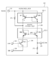
FIG. 2 depicts an embodiment of the voltage regulator depicted in FIG. 1.
FIG. 3 depicts an embodiment of a pin configuration of a packaged IC device.
FIG. 4 is a process flow diagram of a method for operating a voltage regulator in accordance with an embodiment of the invention.
Throughout the description, similar reference numbers may be used to identify similar elements.
It will be readily understood that the components of the embodiments as generally described herein and illustrated in the appended figures could be arranged and designed in a wide variety of different configurations. Thus, the following detailed description of various embodiments, as represented in the figures, is not intended to limit the scope of the present disclosure, but is merely representative of various embodiments. While the various aspects of the embodiments are presented in drawings, the drawings are not necessarily drawn to scale unless specifically indicated.
The described embodiments are to be considered in all respects only as illustrative and not restrictive. The scope of the invention is, therefore, indicated by the appended claims rather than by this detailed description. All changes which come within the meaning and range of equivalency of the claims are to be embraced within their scope.
Reference throughout this specification to features, advantages, or similar language does not imply that all of the features and advantages that may be realized with the present invention should be or are in any single embodiment. Rather, language referring to the features and advantages is understood to mean that a specific feature, advantage, or characteristic described in connection with an embodiment is included in at least one embodiment. Thus, discussions of the features and advantages, and similar language, throughout this specification may, but do not necessarily, refer to the same embodiment.
Furthermore, the described features, advantages, and characteristics of the invention may be combined in any suitable manner in one or more embodiments. One skilled in the relevant art will recognize, in light of the description herein, that the invention can be practiced without one or more of the specific features or advantages of a particular embodiment. In other instances, additional features and advantages may be recognized in certain embodiments that may not be present in all embodiments of the invention.
Reference throughout this specification to “one embodiment,” “an embodiment,” or similar language means that a particular feature, structure, or characteristic described in connection with the indicated embodiment is included in at least one embodiment. Thus, the phrases “in one embodiment,” “in an embodiment,” and similar language throughout this specification may, but do not necessarily, all refer to the same embodiment.
FIG. 1 is a schematic block diagram of a voltage regulator 100 in accordance with an embodiment of the invention. In the embodiment depicted in FIG. 1, the voltage regulator 100 includes two current mirror circuits 102-1, 102-2 and a voltage buffer circuit 104. The voltage regulator converts an input voltage into an output voltage. The input and output voltages can be any suitable type of voltages. In some embodiments, the input and output voltages are direct current (DC) voltages. The voltage regulator can be used to provide an operating voltage for components of an IC. In some embodiments, the voltage regulator converts an input voltage of around (e.g., ±30%) 3.3 Volts (V) into an output voltage of around (e.g., ±30%) 1.8V, and in other embodiments, the voltage regulator converts an input voltage of around 5V into an output voltage of around 1.5V. However, the input and output voltages of the voltage regulator are not limited by the example voltages. Although the voltage regulator is shown in FIG. 1 as including certain components, in some embodiments, the voltage regulator includes less or more components to implement less or more functionalities. For example, in some embodiments, the voltage regulator includes a startup circuit used to generate a startup current.
The current mirror circuits 102-1, 102-2 of the voltage regulator 100 are configured to convert an input voltage into an output voltage. The output voltage of the voltage regulator may be lower than the reference voltage of the voltage regulator or higher than the reference voltage of the voltage regulator. In the embodiment depicted in FIG. 1, the current mirror circuits form the positive feedback loop 106. As shown in FIG. 1, an input terminal, “IN,” of the current mirror circuit 102-1 is connected to an output terminal, “OUT,” of the current mirror circuit 102-2 and an output terminal, “OUT,” of the current mirror circuit 102-1 is connected to an input terminal, “IN,” of the current mirror circuit 102-2. A positive feedback loop is a feedback loop having a positive loop gain. In a positive feedback loop, the feedback is in phase with the input of the feedback loop such that an increase at the input causes a change in the feedback, which in turn causes a larger increase at the input. Because the current mirror circuits form the positive feedback loop, the voltage regulator can be started from a low-power standby mode based on a small quiescent or standby current. The quiescent current in the voltage regulator is the current drawn internally within the voltage regulator. In some embodiments, the quiescent current in the voltage regulator is measured as the input current while no load is connected to the voltage regulator. In some embodiments, the positive feedback loop 106 has a loop gain that is greater than zero but less than 1. Generally, if the loop gain of a feedback loop is greater than 1, the feedback loop can have exponential growth, which causes the feedback loop to be unstable.
The voltage buffer circuit 104 of the voltage regulator 100 is configured to buffer a reference voltage for the current mirror circuits 102-1, 102-2. The reference voltage is generally lower than the input voltage of the voltage regulator. For example, the reference voltage can be about (e.g., ±30%) half of the input voltage of the voltage regulator. In some embodiments, the voltage buffer circuit is used to transfer a voltage from a first circuit (e.g., a reference generation circuit that generates the reference voltage), having a high output impedance, to a second circuit (e.g., the current mirror circuit 102-2) with a low input impedance. The voltage buffer circuit can prevent a circuit at its input from interfering with the desired operation of a circuit at its output. In some embodiments, the voltage buffer circuit includes a source follower circuit.
ICs generally use a voltage regulator circuit that achieves good output voltage regulation in the presence of large load-current variation. Typically, a low-dropout (LDO) regulator is used in an IC to convert an input voltage into a suitable operating voltage for IC components. However, because a LDO regulator has a feedback loop that needs to be stable within the range of load currents and bypass-capacitor values, a certain minimum quiescent current is needed to ensure that the unity gain frequency (UGF) of the LDO regulator is above a certain threshold or to ensure that non-dominant pole-frequencies of the LDO regulator are in an acceptable range. Compared to a conventional voltage regulator, such as an WO regulator, the voltage regulator 100 depicted in FIG. 1 uses the positive feedback loop 106 that is formed by the current mirror circuits 102-1, 102-2 for voltage conversion. Because the current mirror circuits, which form the positive feedback loop, can be simply implemented, the voltage regulator can be implemented using a simplified circuit structure. Consequently, compared to a conventional voltage regulator, the voltage regulator can have a low quiescent or standby current. For example, the voltage regulator can have a quiescent current that is equal to or below 1 microampere (μA). The positive feedback loop formed by the current mirror circuits in general is stable when the loop gain is less than 1. Consequently, the output voltage of the voltage regulator can be reasonably well-regulated.
FIG. 2 depicts an embodiment of the voltage regulator 100 of FIG. 1. In the embodiment depicted in FIG. 2, a DC voltage regulator 200 includes a startup circuit 210, two current mirror circuits 202-1, 202-2 that form a positive loop 206, a voltage buffer circuit 204, and a resistor 212. The voltage regulator 200 depicted in FIG. 2 is one possible embodiment of the voltage regulator 100 depicted in FIG. 1. However, the voltage regulator depicted in FIG. 1 is not limited to the embodiment shown in FIG. 2.
The voltage regulator 200 can have low standby power consumption, high load-current capability, and a reasonable output-voltage compliance range. For example, the voltage regulator can have a quiescent current on the order of 1 μA while supporting a load in the range of several hundred microamperes. Consequently, the voltage regulator can provide sufficient processing power to detect the need to exit a low-power mode and to enable a full-fledged LDO. Although in some cases the output voltage of the voltage regulator may not be well regulated (e.g., the output voltage can be low for a low load) and the voltage regulator may not be a low-dropout solution (e.g., the input voltage may be higher than 2.9V), the voltage regulator can be used to replace an LDO in a low-power-mode.
In an embodiment, the voltage regulator 200 converts an input voltage, “VDD3V3,” into an output voltage, “VDD1V8.” The system power supply voltage may typically be 3.3V while the operating voltage for digital logic cells is typically 1.8V. In the embodiment depicted in FIG. 2, the voltage regulator receives an input voltage of 3.3V and outputs an output voltage of 1.8V. However, in other embodiments, the input and output voltages of the voltage regulator have other values.
In an embodiment, because the voltage regulator 200 uses the positive feedback loop 206, the startup circuit 210 is used to generate an initial startup current because “no current” is also a stable state. In some embodiments, the startup circuit is implemented as a resistor 210 with large resistance (e.g., 10-20 mega Ohm). A resistor with a large resistance can help to achieve a low quiescent current. In the embodiment depicted in FIG. 2, the startup circuit is connected to an input terminal 232, from which the input voltage, “VDD3V3,” is input into the voltage regulator.
The current mirror circuits 202-1, 202-2 of the voltage regulator 200 are configured to perform voltage down-conversion. The current mirror circuit 202-1 includes PMOS transistors, “MP1,” “MP2” while the current mirror circuit 202-2 includes NMOS transistors, “MN0,” “MN3.” In the current mirror circuit 202-1, gate terminals, “G,” of the PMOS transistors, “MP1,” “MP2,” are connected to each other and the gate terminal, “G,” of the PMOS transistor, “MP2,” is connected to the drain terminal, “D,” of the PMOS transistor, “MP2.” In the current mirror circuit 202-2, gate terminals, “G,” of the NMOS transistors, “MN0,” “MN3,” are connected to each other and the gate terminal, “G,” of the NMOS transistor, “MN0,” is connected to the drain terminal, “D,” of the NMOS transistor, “MN0.” The current mirror circuits 202-1, 202-2 form the positive feedback loop 206 with a loop gain that is greater than zero but less than 1. Because the positive feedback loop has a loop gain that is less than 1, the voltage regulator operates as a high gain structure in closed-loop, thereby providing good load regulation. In the embodiment depicted in FIG. 2, the drain terminal, “D,” of the PMOS transistor, “MP1,” is connected to the drain terminal, “D,” of the NMOS transistor, “MN0,” while the drain terminal, “D,” of the PMOS transistor, “MP3,” is connected to the drain terminal, “D,” of the NMOS transistor, “MN3.”
The voltage buffer circuit 204 of the voltage regulator 200 is configured to buffer a reference voltage, “Vref,” for the current mirror circuits 202-1, 202-2. In an embodiment, the reference voltage, “Vref,” is set to be below 1.5V (e.g., 1.25V). In the embodiment depicted in FIG. 2, the voltage buffer circuit 204 is implemented as a source follower PMOS transistor, “MP0,” whose output (i.e., the signal at the source terminal, “S,” of the PMOS transistor, “MP0,”) is connected to the positive feedback loop 206 formed by the current mirror circuits 202-1, 202-2. In some embodiments, the output voltage of the voltage regulator is approximately a PMOS voltage threshold above the reference voltage, “Vref.” As shown in FIG. 2, the gate terminal, “G,” of the source follower transistor, “MP0,” is connected to a reference terminal 236, from which the reference voltage, “Vref,” is input into the voltage regulator, the drain terminal, “D,” of the source follower transistor, “MP0,” is connected to a ground terminal 238, “gnd,” and the source terminal, “S,” of the source follower transistor, “MP0,” is connected to the source terminal, “S,” of the transistor, “MN0,” of the current mirror circuit 202-2.
The resistor 212 of the voltage regulator 200, which may be optional in some embodiments, is used to ensure minimum current in the current mirror circuits 202-1, 202-2. In the embodiment depicted in FIG. 2, the resistor 212 is connected to the positive feedback loop 206 formed by the current mirror circuits 202-1, 202-2 and to an output terminal 234, from which the output voltage, “VDD1V8,” of the voltage regulator is output. In some embodiments, the resistor has a large resistance (e.g., 10-20 mega Ohm).
An example of the operation of the voltage regulator 200 is described as follows. When a load circuit (not shown) draws current from the output terminal 234 of the voltage regulator, the source voltage of the NMOS transistor, “MN3,” instantaneously reduces. The lowering of the source voltage of the NMOS transistor, “MN3,” (thereby increasing its gate to source voltage (VGS)) allows the NMOS transistor, “MN3,” to supply the increased load demand. The increased load current at the output terminal 234 also flows out of the current mirror circuit 202-1 formed by the PMOS transistors, “MP1,” “MP2.” Consequently, the increased load current (ratioed down because the transistors, “MP2,” “MP3,” are typically larger than the transistors, “MP1,” “MN0”) flows in the NMOS transistor, “MN0,” which causes the VGS of the NMOS transistor, “MN0,” to increase because of the increase of its drain current, and causes the source voltage of the NMOS transistor, “MN0,” to increase due to the non-zero output resistance of the source-follower, “MP0.” Consequently, the gate voltage of the NMOS transistor, “MN3,” is increased and the source voltage of the NMOS transistor, “MN3,” is restored to a value that corresponds to acceptable voltage regulation.
In some embodiments, the voltage regulator 200 depicted in FIG. 2 can be embodied in a packaged IC device. FIG. 3 depicts an embodiment of a packaged IC device 330. In the embodiment depicted in FIG. 3, the pin configuration of the packaged IC device includes an input voltage pin 332, an output voltage pin 334, a reference voltage pin 336, and a ground pin 335. The packaged IC device depicted in FIG. 3 is one possible packaged IC device of the voltage regulator depicted in FIG. 2. However, the packaged IC device of the voltage regulator is not limited to the embodiment shown in FIG. 3.
FIG. 4 is a process flow diagram of a method for operating a voltage regulator in accordance with an embodiment of the invention. The voltage regulator may be similar to or the same as the voltage regulator 100 depicted in FIG. 1 and/or the voltage regulator 200 depicted in FIG. 2. At block 402, a reference voltage is buffered for a set of current mirror circuits. At block 404, an input voltage is converted into an output voltage using the set of current mirror circuits, where the set of current mirror circuits form a positive feedback loop.
Although the operations of the method herein are shown and described in a particular order, the order of the operations of the method may be altered so that certain operations may be performed in an inverse order or so that certain operations may be performed, at least in part, concurrently with other operations. In another embodiment, instructions or sub-operations of distinct operations may be implemented in an intermittent and/or alternating manner.
In addition, although specific embodiments of the invention that have been described or depicted include several components described or depicted herein, other embodiments of the invention may include fewer or more components to implement less or more features.
Furthermore, although specific embodiments of the invention have been described and depicted, the invention is not to be limited to the specific forms or arrangements of parts so described and depicted. The scope of the invention is to be defined by the claims appended hereto and their equivalents.

Claims (20)

What is claimed is:
1. A voltage regulator, the voltage regulator comprising:
a set of current mirror circuits configured to convert an input voltage into an output voltage, wherein the set of current mirror circuits form a positive feedback loop; and
a voltage buffer circuit configured to buffer a fixed reference voltage for the set of current mirror circuits,
wherein the voltage buffer circuit comprises a source follower transistor connected between the fixed reference voltage and a source terminal of a transistor device of the set of current mirror circuits,
wherein a drain terminal of the source follower transistor is directly connected to a second fixed reference voltage;
wherein the second fixed reference voltage is zero volt, and
wherein the drain terminal of the source follower transistor is directly connected to ground.
2. The voltage regulator of claim 1, wherein the positive feedback loop has a loop gain that is less than 1.
3. The voltage regulator of claim 1, wherein the output voltage is lower than the input voltage.
4. The voltage regulator of claim 1, wherein the input and output voltages are direct current (DC) voltages.
5. The voltage regulator of claim 1,
wherein the set of current mirror circuits comprises a first current mirror circuit and a second current mirror circuit,
wherein an input terminal of the first current mirror circuit is connected to an output terminal of the second current mirror and an output terminal of the first current mirror circuit is connected to an input terminal of the second current mirror circuit.
6. The voltage regulator of claim 5,
wherein the first current mirror circuit comprises a first PMOS transistor and a second PMOS transistor, and
wherein the second current mirror circuit comprises a first NMOS transistor and a second NMOS transistor.
7. The voltage regulator of claim 5,
wherein gate terminals of the first and second PMOS transistors are connected to each other, and
wherein the gate terminal of the second PMOS transistor is connected to a drain terminal of the second PMOS transistor.
8. The voltage regulator of claim 7,
wherein gate terminals of the first and second NMOS transistors are connected to each other, and
wherein the gate terminal of the first NMOS transistor is connected to a drain terminal of the first NMOS transistor.
9. The voltage regulator of claim 8,
wherein a drain terminal of the first PMOS transistor is connected to a drain terminal of the first NMOS transistor, and
wherein the drain terminal of the second PMOS transistor is connected to the drain terminal of the second NMOS transistor.
10. The voltage regulator of claim 1, wherein the fixed reference voltage is lower than the input voltage and the output voltage.
11. The voltage regulator of claim 1, further comprising a startup circuit configured to generate a startup current for the set of current mirror circuits.
12. The voltage regulator of claim 11,
wherein the startup circuit comprises a resistor connected to an input terminal, from which the input voltage is input into the voltage regulator, and to the set of current mirror circuits.
13. The voltage regulator of claim 1, further comprising
a resistor connected to an output terminal, from which the output voltage is output from the voltage regulator, and to the set of current mirror circuits.
14. The voltage regulator of claim 1, wherein the input voltage is around 3.3V and the output voltage is around 1.8V.
15. The voltage regulator of claim 1,
wherein the source follower transistor comprises a PMOS transistor,
wherein a source terminal of the PMOS transistor is connected to the source terminal of the transistor device,
wherein a drain terminal of the PMOS transistor is connected to a fixed voltage, and
wherein a gate terminal of the PMOS transistor is connected to a reference terminal from which the fixed reference voltage is input into the voltage regulator.
16. A voltage regulator, the voltage regulator comprising:
a set of current mirror circuits configured to convert an input direct current (DC) voltage into an output DC voltage,
wherein the set of current mirror circuits form a positive feedback loop having a loop gain that is less than 1, and wherein the output voltage is lower than the input voltage; and
a voltage buffer circuit configured to buffer a fixed reference DC voltage for the set of current mirror circuits,
wherein the voltage buffer circuit comprises a source follower transistor connected between the fixed reference DC voltage and a source terminal of a transistor device of the set of current mirror circuits, and
wherein a drain terminal of the source follower transistor is directly connected to a second fixed reference voltage;
wherein the second fixed reference voltage is zero volt, and
wherein the drain terminal of the source follower transistor is directly connected to ground.
17. The voltage regulator of claim 16,
wherein the set of current mirror circuits comprises a first current mirror circuit and a second current mirror circuit,
wherein the first current mirror circuit comprises a first PMOS transistor and a second PMOS transistor,
wherein the second current mirror circuit comprises a first NMOS transistor and a second NMOS transistor,
wherein gate terminals of the first and second PMOS transistors are connected to each other,
wherein the gate terminal of the second PMOS transistor is connected to a drain terminal of the second PMOS transistor,
wherein gate terminals of the first and second NMOS transistors are connected to each other,
wherein the gate terminal of the first NMOS transistor is connected to a drain terminal of the first NMOS transistor,
wherein a drain terminal of the first PMOS transistor is connected to a drain terminal of the first NMOS transistor, and
wherein the drain terminal of the second PMOS transistor is connected to the drain terminal of the second NMOS transistor.
18. The voltage regulator of claim 17,
further comprising a startup circuit configured to generate a startup current for the set of current mirror circuits, and
wherein the startup circuit comprises a resistor connected to an input terminal, from which the input voltage is input into the voltage regulator, and to the set of current mirror circuits.
19. The voltage regulator of claim 17, wherein the input voltage is around 3.3V and the output voltage is around 1.8V.
20. A method for operating a voltage regulator, the method comprising:
buffering a fixed reference voltage for a set of current mirror circuits using a source follower transistor connected between the fixed reference voltage and a source terminal of a transistor device of the set of current mirror circuits, and
wherein a drain terminal of the source follower transistor is directly connected to a second fixed reference voltage;
wherein the second fixed reference voltage is zero volt, and
wherein the drain terminal of the source follower transistor is directly connected to ground; and
converting an input voltage into an output voltage using the set of current mirror circuits,
wherein the set of current mirror circuits form a positive feedback loop.
US14/533,555 2014-11-05 2014-11-05 Low quiescent current voltage regulator with high load-current capability Active 2035-01-08 US9817426B2 (en)

Priority Applications (3)

Application Number Priority Date Filing Date Title
US14/533,555 US9817426B2 (en) 2014-11-05 2014-11-05 Low quiescent current voltage regulator with high load-current capability
EP15187595.2A EP3018551A1 (en) 2014-11-05 2015-09-30 Low quiescent current voltage regulator with high load-current capacity
CN201510726136.5A CN105573394B (en) 2014-11-05 2015-10-30 Low silent current voltage regulator with high load currents ability

Applications Claiming Priority (1)

Application Number Priority Date Filing Date Title
US14/533,555 US9817426B2 (en) 2014-11-05 2014-11-05 Low quiescent current voltage regulator with high load-current capability

Publications (2)

Publication Number Publication Date
US20160124454A1 US20160124454A1 (en) 2016-05-05
US9817426B2 true US9817426B2 (en) 2017-11-14

Family

ID=54252079

Family Applications (1)

Application Number Title Priority Date Filing Date
US14/533,555 Active 2035-01-08 US9817426B2 (en) 2014-11-05 2014-11-05 Low quiescent current voltage regulator with high load-current capability

Country Status (3)

Country Link
US (1) US9817426B2 (en)
EP (1) EP3018551A1 (en)
CN (1) CN105573394B (en)

Cited By (5)

* Cited by examiner, † Cited by third party
Publication number Priority date Publication date Assignee Title
US11502683B2 (en) 2021-04-14 2022-11-15 Skyworks Solutions, Inc. Calibration of driver output current
US11556144B2 (en) 2020-12-16 2023-01-17 Skyworks Solutions, Inc. High-speed low-impedance boosting low-dropout regulator
US11561563B2 (en) * 2020-12-11 2023-01-24 Skyworks Solutions, Inc. Supply-glitch-tolerant regulator
US11817854B2 (en) 2020-12-14 2023-11-14 Skyworks Solutions, Inc. Generation of positive and negative switch gate control voltages
US12068687B2 (en) 2021-10-15 2024-08-20 Advanced Micro Devices, Inc. Method to reduce overshoot in a voltage regulating power supply

Families Citing this family (10)

* Cited by examiner, † Cited by third party
Publication number Priority date Publication date Assignee Title
US9575498B2 (en) * 2015-01-29 2017-02-21 Qualcomm Incorporated Low dropout regulator bleeding current circuits and methods
JP6100931B1 (en) * 2016-01-12 2017-03-22 トレックス・セミコンダクター株式会社 Reference voltage generation circuit
DE102017207998B3 (en) 2017-05-11 2018-08-30 Dialog Semiconductor (Uk) Limited Voltage regulator and method for providing an output voltage with reduced voltage ripple
TWI674493B (en) * 2018-05-25 2019-10-11 新加坡商光寶科技新加坡私人有限公司 Low-dropout shunt voltage regulator
US11287839B2 (en) 2019-09-25 2022-03-29 Apple Inc. Dual loop LDO voltage regulator
CN111313852B (en) * 2020-05-15 2020-09-11 微龛(广州)半导体有限公司 Drive amplifier and analog-to-digital converter
US11960311B2 (en) 2020-07-28 2024-04-16 Medtronic Minimed, Inc. Linear voltage regulator with isolated supply current
CN112328000B (en) * 2020-09-30 2022-08-26 江苏清微智能科技有限公司 Ultra-low quiescent current quick response circuit and device
CN112530365A (en) * 2020-12-17 2021-03-19 北京集创北方科技股份有限公司 Power supply circuit, chip and display screen
US11927624B2 (en) * 2021-06-25 2024-03-12 Texas Instruments Incorporated Method for measuring quiescent current in a switching voltage regulator

Citations (19)

* Cited by examiner, † Cited by third party
Publication number Priority date Publication date Assignee Title
US4929884A (en) * 1987-06-08 1990-05-29 U.S. Philips Corp. High voltage semiconductor with integrated low voltage circuitry
US5180927A (en) 1990-11-20 1993-01-19 Sgs-Thomson Microelectronics S.R.L. Reset device for microprocessor, particularly for automotive applications
US5180967A (en) 1990-08-03 1993-01-19 Oki Electric Industry Co., Ltd. Constant-current source circuit having a mos transistor passing off-heat current
EP0766003A2 (en) 1995-09-29 1997-04-02 Mitsuba Corporation Co., Ltd. Ignition system for internal combustion engines
US5640122A (en) * 1994-12-16 1997-06-17 Sgs-Thomson Microelectronics, Inc. Circuit for providing a bias voltage compensated for p-channel transistor variations
US5986507A (en) * 1995-09-12 1999-11-16 Kabushiki Kaisha Toshiba Current mirror circuit
US6191646B1 (en) * 1998-06-30 2001-02-20 Hyundai Electronics Industries Co., Ltd. Temperature compensated high precision current source
EP1126350A1 (en) 2000-02-15 2001-08-22 Infineon Technologies AG Voltage-to-current converter
US6359427B1 (en) * 2000-08-04 2002-03-19 Maxim Integrated Products, Inc. Linear regulators with low dropout and high line regulation
US20040041622A1 (en) 2002-08-27 2004-03-04 Winsbond Electronics Corporation Stable current source circuit with compensation circuit
US20040164790A1 (en) * 2003-02-24 2004-08-26 Samsung Electronics Co., Ltd. Bias circuit having a start-up circuit
US20050237104A1 (en) 2004-04-27 2005-10-27 Taiwan Semiconductor Manufacturing Company, Ltd. Reference voltage generator circuit having temperature and process variation compensation and method of manufacturing same
CN200997085Y (en) 2006-12-30 2007-12-26 Bcd半导体制造有限公司 Low-consumption current source circuit
US20100283448A1 (en) * 2009-05-06 2010-11-11 Texas Instruments Incorporated Reference circuit with reduced current startup
US20120025883A1 (en) * 2010-07-30 2012-02-02 Guangyuan Lin Lock detection circuit and phase-locked loop circuit including the same
CN102455731A (en) 2010-10-21 2012-05-16 曹先国 Low-supply voltage sensitivity reference offset
US20120139637A1 (en) * 2010-12-07 2012-06-07 Korea Advanced Institute Of Science And Technology Linear amplifier
CN104102266A (en) 2014-07-11 2014-10-15 南京芯力微电子有限公司 Reference voltage generating circuit
US20150002110A1 (en) * 2013-06-27 2015-01-01 Stmicroelectronics International N.V. Voltage Regulator

Family Cites Families (1)

* Cited by examiner, † Cited by third party
Publication number Priority date Publication date Assignee Title
JP3556328B2 (en) * 1995-07-11 2004-08-18 株式会社ルネサステクノロジ Internal power supply circuit

Patent Citations (21)

* Cited by examiner, † Cited by third party
Publication number Priority date Publication date Assignee Title
US4929884A (en) * 1987-06-08 1990-05-29 U.S. Philips Corp. High voltage semiconductor with integrated low voltage circuitry
US5180967A (en) 1990-08-03 1993-01-19 Oki Electric Industry Co., Ltd. Constant-current source circuit having a mos transistor passing off-heat current
US5180927A (en) 1990-11-20 1993-01-19 Sgs-Thomson Microelectronics S.R.L. Reset device for microprocessor, particularly for automotive applications
US5640122A (en) * 1994-12-16 1997-06-17 Sgs-Thomson Microelectronics, Inc. Circuit for providing a bias voltage compensated for p-channel transistor variations
US5986507A (en) * 1995-09-12 1999-11-16 Kabushiki Kaisha Toshiba Current mirror circuit
EP0766003A2 (en) 1995-09-29 1997-04-02 Mitsuba Corporation Co., Ltd. Ignition system for internal combustion engines
CN1152671A (en) 1995-09-29 1997-06-25 株式会社美姿把 Ignition system for internal combustion engines
US6191646B1 (en) * 1998-06-30 2001-02-20 Hyundai Electronics Industries Co., Ltd. Temperature compensated high precision current source
US6586919B2 (en) 2000-02-15 2003-07-01 Infineon Technologies Ag Voltage-current converter
EP1126350A1 (en) 2000-02-15 2001-08-22 Infineon Technologies AG Voltage-to-current converter
US6359427B1 (en) * 2000-08-04 2002-03-19 Maxim Integrated Products, Inc. Linear regulators with low dropout and high line regulation
US20040041622A1 (en) 2002-08-27 2004-03-04 Winsbond Electronics Corporation Stable current source circuit with compensation circuit
US20040164790A1 (en) * 2003-02-24 2004-08-26 Samsung Electronics Co., Ltd. Bias circuit having a start-up circuit
US20050237104A1 (en) 2004-04-27 2005-10-27 Taiwan Semiconductor Manufacturing Company, Ltd. Reference voltage generator circuit having temperature and process variation compensation and method of manufacturing same
CN200997085Y (en) 2006-12-30 2007-12-26 Bcd半导体制造有限公司 Low-consumption current source circuit
US20100283448A1 (en) * 2009-05-06 2010-11-11 Texas Instruments Incorporated Reference circuit with reduced current startup
US20120025883A1 (en) * 2010-07-30 2012-02-02 Guangyuan Lin Lock detection circuit and phase-locked loop circuit including the same
CN102455731A (en) 2010-10-21 2012-05-16 曹先国 Low-supply voltage sensitivity reference offset
US20120139637A1 (en) * 2010-12-07 2012-06-07 Korea Advanced Institute Of Science And Technology Linear amplifier
US20150002110A1 (en) * 2013-06-27 2015-01-01 Stmicroelectronics International N.V. Voltage Regulator
CN104102266A (en) 2014-07-11 2014-10-15 南京芯力微电子有限公司 Reference voltage generating circuit

Non-Patent Citations (11)

* Cited by examiner, † Cited by third party
Title
Extended European Search Report for Patent Appln. No. 15187595.2 (dated Mar. 8, 2016).
Linear Technology; "Monolithic 3A, 1.25MHz Step-Down Switching Regulator"; LT0608 Rev. D; 20 pgs.; 2001.
Office Action from counterpart application CN201510726136.5; 9 pages (dated Sep. 1, 2016).
ON Semiconductor; "200 mA, Ultra-Low Quiescent Current, Ultra-Low Noise, LDO Linear Voltage Regulator"; NCP702; Semiconductor Components Industries, LLC, 2013; 20 pgs.; Revision; Jul. 2013.
Stlife.augmented; "150 mA, ultra low quiescent current linear voltage regulator"; Datasheet-production data; STLQ015; DocID17285 Rev 4 1; 16 pgs.; Feb. 2014.
Stlife.augmented; "150 mA, ultra low quiescent current linear voltage regulator"; Datasheet—production data; STLQ015; DocID17285 Rev 4 1; 16 pgs.; Feb. 2014.
Texas Instruments; ""500nA IQ, 150mA, Ultra-Low Quiescent CurrentLow-Dropout Linear Regulator""; TPS783xx, SBVS133; Feb. 2010.
Texas Instruments; "LM1086 1.5A Low Dropout Positive Regulators; LM1086; 24 pgs.; SNVS039H-Jun. 2000; Revised May 2013".
Texas Instruments; "SM74501 Ultra-Low Quiescent Current LDO Voltage Regulator"; SNVS721B-Jun. 2011; 10 pgs.; Revised Apr. 2013.
Texas Instruments; "LM1086 1.5A Low Dropout Positive Regulators; LM1086; 24 pgs.; SNVS039H—Jun. 2000; Revised May 2013".
Texas Instruments; "SM74501 Ultra-Low Quiescent Current LDO Voltage Regulator"; SNVS721B—Jun. 2011; 10 pgs.; Revised Apr. 2013.

Cited By (10)

* Cited by examiner, † Cited by third party
Publication number Priority date Publication date Assignee Title
US11561563B2 (en) * 2020-12-11 2023-01-24 Skyworks Solutions, Inc. Supply-glitch-tolerant regulator
US11815928B2 (en) 2020-12-11 2023-11-14 Skyworks Solutions, Inc. Supply-glitch-tolerant regulator
US12045075B2 (en) 2020-12-11 2024-07-23 Skyworks Solutions, Inc. Supply-glitch-tolerant regulator
US11817854B2 (en) 2020-12-14 2023-11-14 Skyworks Solutions, Inc. Generation of positive and negative switch gate control voltages
US11556144B2 (en) 2020-12-16 2023-01-17 Skyworks Solutions, Inc. High-speed low-impedance boosting low-dropout regulator
US11822360B2 (en) 2020-12-16 2023-11-21 Skyworks Solutions, Inc. High-speed low-impedance boosting low-dropout regulator
US12339690B2 (en) 2020-12-16 2025-06-24 Skyworks Solutions, Inc. High-speed low-impedance boosting low-dropout regulator
US11502683B2 (en) 2021-04-14 2022-11-15 Skyworks Solutions, Inc. Calibration of driver output current
US11962294B2 (en) 2021-04-14 2024-04-16 Skyworks Solutions, Inc. Calibration of driver output current
US12068687B2 (en) 2021-10-15 2024-08-20 Advanced Micro Devices, Inc. Method to reduce overshoot in a voltage regulating power supply

Also Published As

Publication number Publication date
US20160124454A1 (en) 2016-05-05
CN105573394A (en) 2016-05-11
EP3018551A1 (en) 2016-05-11
CN105573394B (en) 2018-10-23

Similar Documents

Publication Publication Date Title
US9817426B2 (en) Low quiescent current voltage regulator with high load-current capability
US9030186B2 (en) Bandgap reference circuit and regulator circuit with common amplifier
US9454166B2 (en) LDO regulator with improved load transient performance for internal power supply
JP5516320B2 (en) Semiconductor integrated circuit for regulator
US8129966B2 (en) Voltage regulator circuit and control method therefor
TWI621326B (en) Linear regulator with improved power supply ripple rejection, method thereof and circuit to provide a voltage reference
US20120223688A1 (en) High power supply rejection ratio (psrr) and low dropout regulator
US10958160B2 (en) Feedback scheme for stable LDO regulator operation
CN103092243A (en) Signal generating circuit
US9342085B2 (en) Circuit for regulating startup and operation voltage of an electronic device
TWI514104B (en) Current source for voltage regulator and voltage regulator thereof
KR101274280B1 (en) Voltage regulator
US20200409402A1 (en) Reference voltage generation
US20180292853A1 (en) Quiescent Current Control in Voltage Regulators
CN110945453A (en) LDO, MCU, fingerprint module and terminal equipment
US20110309808A1 (en) Bias-starving circuit with precision monitoring loop for voltage regulators with enhanced stability
JP6038100B2 (en) Semiconductor integrated circuit
CN101930244B (en) Low dropout regulator and method for improving its power supply rejection ratio
US9753480B2 (en) Voltage regulators
US12411510B2 (en) Low-power fast-transient low-dropout (LDO) regulator with direct feed-forward
Moon et al. Design of low-power, fast-transient-response, capacitor-less low-dropout regulator for mobile applications
Ameziane et al. Full on-chip low dropout voltage regulator with an enhanced transient response for low power systems
Chen et al. 17.10 0.65 V-input-voltage 0.6 V-output-voltage 30ppm/° C low-dropout regulator with embedded voltage reference for low-power biomedical systems
US8872490B2 (en) Voltage regulator
US10658984B2 (en) Differential amplifier circuit

Legal Events

Date Code Title Description
AS Assignment

Owner name: NXP B.V., NETHERLANDS

Free format text: ASSIGNMENT OF ASSIGNORS INTEREST;ASSIGNOR:CHELLAPPA, ANANTHASAYANAM;REEL/FRAME:034108/0765

Effective date: 20141104

STCF Information on status: patent grant

Free format text: PATENTED CASE

MAFP Maintenance fee payment

Free format text: PAYMENT OF MAINTENANCE FEE, 4TH YEAR, LARGE ENTITY (ORIGINAL EVENT CODE: M1551); ENTITY STATUS OF PATENT OWNER: LARGE ENTITY

Year of fee payment: 4

MAFP Maintenance fee payment

Free format text: PAYMENT OF MAINTENANCE FEE, 8TH YEAR, LARGE ENTITY (ORIGINAL EVENT CODE: M1552); ENTITY STATUS OF PATENT OWNER: LARGE ENTITY

Year of fee payment: 8