US9812635B2 - Method of manufacturing ultrasound probe - Google Patents
Method of manufacturing ultrasound probe Download PDFInfo
- Publication number
- US9812635B2 US9812635B2 US14/607,884 US201514607884A US9812635B2 US 9812635 B2 US9812635 B2 US 9812635B2 US 201514607884 A US201514607884 A US 201514607884A US 9812635 B2 US9812635 B2 US 9812635B2
- Authority
- US
- United States
- Prior art keywords
- electrode
- piezoelectric unit
- backing layer
- layer
- piezoelectric
- Prior art date
- Legal status (The legal status is an assumption and is not a legal conclusion. Google has not performed a legal analysis and makes no representation as to the accuracy of the status listed.)
- Active, expires
Links
- 238000002604 ultrasonography Methods 0.000 title claims abstract description 73
- 239000000523 sample Substances 0.000 title claims abstract description 36
- 238000004519 manufacturing process Methods 0.000 title claims abstract description 12
- 238000000034 method Methods 0.000 claims abstract description 32
- 239000004020 conductor Substances 0.000 claims description 15
- 238000005137 deposition process Methods 0.000 claims description 9
- 238000005304 joining Methods 0.000 claims description 8
- 230000008569 process Effects 0.000 claims description 7
- 239000000758 substrate Substances 0.000 claims description 5
- 238000000465 moulding Methods 0.000 claims description 4
- 239000010410 layer Substances 0.000 description 120
- 238000003860 storage Methods 0.000 description 11
- 238000010586 diagram Methods 0.000 description 8
- 239000000463 material Substances 0.000 description 6
- 230000015654 memory Effects 0.000 description 5
- XOLBLPGZBRYERU-UHFFFAOYSA-N tin dioxide Chemical compound O=[Sn]=O XOLBLPGZBRYERU-UHFFFAOYSA-N 0.000 description 5
- 238000000151 deposition Methods 0.000 description 4
- 238000005530 etching Methods 0.000 description 4
- 125000005678 ethenylene group Chemical group [H]C([*:1])=C([H])[*:2] 0.000 description 4
- 238000007517 polishing process Methods 0.000 description 4
- -1 poly p-phenylene Polymers 0.000 description 4
- 238000004544 sputter deposition Methods 0.000 description 4
- OKTJSMMVPCPJKN-UHFFFAOYSA-N Carbon Chemical compound [C] OKTJSMMVPCPJKN-UHFFFAOYSA-N 0.000 description 3
- 241001465754 Metazoa Species 0.000 description 3
- 239000010949 copper Substances 0.000 description 3
- JAONJTDQXUSBGG-UHFFFAOYSA-N dialuminum;dizinc;oxygen(2-) Chemical compound [O-2].[O-2].[O-2].[O-2].[O-2].[Al+3].[Al+3].[Zn+2].[Zn+2] JAONJTDQXUSBGG-UHFFFAOYSA-N 0.000 description 3
- 239000010931 gold Substances 0.000 description 3
- 229910003437 indium oxide Inorganic materials 0.000 description 3
- PJXISJQVUVHSOJ-UHFFFAOYSA-N indium(iii) oxide Chemical compound [O-2].[O-2].[O-2].[In+3].[In+3] PJXISJQVUVHSOJ-UHFFFAOYSA-N 0.000 description 3
- 239000010409 thin film Substances 0.000 description 3
- 239000004734 Polyphenylene sulfide Substances 0.000 description 2
- HSFWRNGVRCDJHI-UHFFFAOYSA-N alpha-acetylene Natural products C#C HSFWRNGVRCDJHI-UHFFFAOYSA-N 0.000 description 2
- 229910002113 barium titanate Inorganic materials 0.000 description 2
- 239000002717 carbon nanostructure Substances 0.000 description 2
- 239000002041 carbon nanotube Substances 0.000 description 2
- 230000006835 compression Effects 0.000 description 2
- 238000007906 compression Methods 0.000 description 2
- 229920001940 conductive polymer Polymers 0.000 description 2
- 229910052802 copper Inorganic materials 0.000 description 2
- 238000001514 detection method Methods 0.000 description 2
- 238000003745 diagnosis Methods 0.000 description 2
- 230000000694 effects Effects 0.000 description 2
- 230000006870 function Effects 0.000 description 2
- 229910052737 gold Inorganic materials 0.000 description 2
- 229910021389 graphene Inorganic materials 0.000 description 2
- 229910052451 lead zirconate titanate Inorganic materials 0.000 description 2
- 229910052751 metal Inorganic materials 0.000 description 2
- 239000002184 metal Substances 0.000 description 2
- 239000002082 metal nanoparticle Substances 0.000 description 2
- 229910044991 metal oxide Inorganic materials 0.000 description 2
- 150000004706 metal oxides Chemical class 0.000 description 2
- 150000002739 metals Chemical class 0.000 description 2
- 238000007747 plating Methods 0.000 description 2
- 229920001197 polyacetylene Polymers 0.000 description 2
- 229920000767 polyaniline Polymers 0.000 description 2
- 229920000069 polyphenylene sulfide Polymers 0.000 description 2
- 229920000128 polypyrrole Polymers 0.000 description 2
- 229920000123 polythiophene Polymers 0.000 description 2
- 229910052709 silver Inorganic materials 0.000 description 2
- 238000007738 vacuum evaporation Methods 0.000 description 2
- 238000007740 vapor deposition Methods 0.000 description 2
- PIGFYZPCRLYGLF-UHFFFAOYSA-N Aluminum nitride Chemical compound [Al]#N PIGFYZPCRLYGLF-UHFFFAOYSA-N 0.000 description 1
- RYGMFSIKBFXOCR-UHFFFAOYSA-N Copper Chemical compound [Cu] RYGMFSIKBFXOCR-UHFFFAOYSA-N 0.000 description 1
- 229910019653 Mg1/3Nb2/3 Inorganic materials 0.000 description 1
- 206010028980 Neoplasm Diseases 0.000 description 1
- 229910003781 PbTiO3 Inorganic materials 0.000 description 1
- BQCADISMDOOEFD-UHFFFAOYSA-N Silver Chemical compound [Ag] BQCADISMDOOEFD-UHFFFAOYSA-N 0.000 description 1
- RTAQQCXQSZGOHL-UHFFFAOYSA-N Titanium Chemical compound [Ti] RTAQQCXQSZGOHL-UHFFFAOYSA-N 0.000 description 1
- 208000027418 Wounds and injury Diseases 0.000 description 1
- XLOMVQKBTHCTTD-UHFFFAOYSA-N Zinc monoxide Chemical compound [Zn]=O XLOMVQKBTHCTTD-UHFFFAOYSA-N 0.000 description 1
- 210000001015 abdomen Anatomy 0.000 description 1
- 229910052782 aluminium Inorganic materials 0.000 description 1
- 238000013459 approach Methods 0.000 description 1
- JRPBQTZRNDNNOP-UHFFFAOYSA-N barium titanate Chemical compound [Ba+2].[Ba+2].[O-][Ti]([O-])([O-])[O-] JRPBQTZRNDNNOP-UHFFFAOYSA-N 0.000 description 1
- 230000008901 benefit Effects 0.000 description 1
- 210000004204 blood vessel Anatomy 0.000 description 1
- 210000004556 brain Anatomy 0.000 description 1
- 210000000481 breast Anatomy 0.000 description 1
- 229910021393 carbon nanotube Inorganic materials 0.000 description 1
- 230000008859 change Effects 0.000 description 1
- 238000005520 cutting process Methods 0.000 description 1
- 230000006378 damage Effects 0.000 description 1
- 238000013461 design Methods 0.000 description 1
- 238000002059 diagnostic imaging Methods 0.000 description 1
- NKZSPGSOXYXWQA-UHFFFAOYSA-N dioxido(oxo)titanium;lead(2+) Chemical compound [Pb+2].[O-][Ti]([O-])=O NKZSPGSOXYXWQA-UHFFFAOYSA-N 0.000 description 1
- 229920001971 elastomer Polymers 0.000 description 1
- 230000005672 electromagnetic field Effects 0.000 description 1
- 239000003822 epoxy resin Substances 0.000 description 1
- 210000003754 fetus Anatomy 0.000 description 1
- 230000014509 gene expression Effects 0.000 description 1
- PCHJSUWPFVWCPO-UHFFFAOYSA-N gold Chemical compound [Au] PCHJSUWPFVWCPO-UHFFFAOYSA-N 0.000 description 1
- AMGQUBHHOARCQH-UHFFFAOYSA-N indium;oxotin Chemical compound [In].[Sn]=O AMGQUBHHOARCQH-UHFFFAOYSA-N 0.000 description 1
- 208000014674 injury Diseases 0.000 description 1
- 229910052746 lanthanum Inorganic materials 0.000 description 1
- FZLIPJUXYLNCLC-UHFFFAOYSA-N lanthanum atom Chemical compound [La] FZLIPJUXYLNCLC-UHFFFAOYSA-N 0.000 description 1
- HFGPZNIAWCZYJU-UHFFFAOYSA-N lead zirconate titanate Chemical compound [O-2].[O-2].[O-2].[O-2].[O-2].[Ti+4].[Zr+4].[Pb+2] HFGPZNIAWCZYJU-UHFFFAOYSA-N 0.000 description 1
- 239000004973 liquid crystal related substance Substances 0.000 description 1
- 210000004185 liver Anatomy 0.000 description 1
- 238000005259 measurement Methods 0.000 description 1
- 238000012986 modification Methods 0.000 description 1
- 230000004048 modification Effects 0.000 description 1
- 238000012544 monitoring process Methods 0.000 description 1
- 230000003287 optical effect Effects 0.000 description 1
- 210000000056 organ Anatomy 0.000 description 1
- 230000010355 oscillation Effects 0.000 description 1
- ZBSCCQXBYNSKPV-UHFFFAOYSA-N oxolead;oxomagnesium;2,4,5-trioxa-1$l^{5},3$l^{5}-diniobabicyclo[1.1.1]pentane 1,3-dioxide Chemical compound [Mg]=O.[Pb]=O.[Pb]=O.[Pb]=O.O1[Nb]2(=O)O[Nb]1(=O)O2 ZBSCCQXBYNSKPV-UHFFFAOYSA-N 0.000 description 1
- 238000000059 patterning Methods 0.000 description 1
- 150000003071 polychlorinated biphenyls Chemical class 0.000 description 1
- 229920000647 polyepoxide Polymers 0.000 description 1
- 230000008439 repair process Effects 0.000 description 1
- 230000004044 response Effects 0.000 description 1
- 238000000926 separation method Methods 0.000 description 1
- 229920002379 silicone rubber Polymers 0.000 description 1
- 239000004332 silver Substances 0.000 description 1
- 239000010944 silver (metal) Substances 0.000 description 1
- 239000002356 single layer Substances 0.000 description 1
- 238000000638 solvent extraction Methods 0.000 description 1
- 238000001228 spectrum Methods 0.000 description 1
- 230000003068 static effect Effects 0.000 description 1
- 239000000126 substance Substances 0.000 description 1
- 238000006467 substitution reaction Methods 0.000 description 1
- 238000010897 surface acoustic wave method Methods 0.000 description 1
- 229910001887 tin oxide Inorganic materials 0.000 description 1
- WFKWXMTUELFFGS-UHFFFAOYSA-N tungsten Chemical compound [W] WFKWXMTUELFFGS-UHFFFAOYSA-N 0.000 description 1
- YVTHLONGBIQYBO-UHFFFAOYSA-N zinc indium(3+) oxygen(2-) Chemical compound [O--].[Zn++].[In+3] YVTHLONGBIQYBO-UHFFFAOYSA-N 0.000 description 1
Images


Classifications
-
- A—HUMAN NECESSITIES
- A61—MEDICAL OR VETERINARY SCIENCE; HYGIENE
- A61B—DIAGNOSIS; SURGERY; IDENTIFICATION
- A61B8/00—Diagnosis using ultrasonic, sonic or infrasonic waves
- A61B8/44—Constructional features of the ultrasonic, sonic or infrasonic diagnostic device
- A61B8/4444—Constructional features of the ultrasonic, sonic or infrasonic diagnostic device related to the probe
-
- H—ELECTRICITY
- H10—SEMICONDUCTOR DEVICES; ELECTRIC SOLID-STATE DEVICES NOT OTHERWISE PROVIDED FOR
- H10N—ELECTRIC SOLID-STATE DEVICES NOT OTHERWISE PROVIDED FOR
- H10N30/00—Piezoelectric or electrostrictive devices
- H10N30/01—Manufacture or treatment
- H10N30/07—Forming of piezoelectric or electrostrictive parts or bodies on an electrical element or another base
-
- H01L41/31—
-
- A—HUMAN NECESSITIES
- A61—MEDICAL OR VETERINARY SCIENCE; HYGIENE
- A61B—DIAGNOSIS; SURGERY; IDENTIFICATION
- A61B8/00—Diagnosis using ultrasonic, sonic or infrasonic waves
- A61B8/13—Tomography
- A61B8/14—Echo-tomography
-
- A—HUMAN NECESSITIES
- A61—MEDICAL OR VETERINARY SCIENCE; HYGIENE
- A61B—DIAGNOSIS; SURGERY; IDENTIFICATION
- A61B8/00—Diagnosis using ultrasonic, sonic or infrasonic waves
- A61B8/44—Constructional features of the ultrasonic, sonic or infrasonic diagnostic device
- A61B8/4483—Constructional features of the ultrasonic, sonic or infrasonic diagnostic device characterised by features of the ultrasound transducer
-
- B—PERFORMING OPERATIONS; TRANSPORTING
- B06—GENERATING OR TRANSMITTING MECHANICAL VIBRATIONS IN GENERAL
- B06B—METHODS OR APPARATUS FOR GENERATING OR TRANSMITTING MECHANICAL VIBRATIONS OF INFRASONIC, SONIC, OR ULTRASONIC FREQUENCY, e.g. FOR PERFORMING MECHANICAL WORK IN GENERAL
- B06B1/00—Methods or apparatus for generating mechanical vibrations of infrasonic, sonic, or ultrasonic frequency
- B06B1/02—Methods or apparatus for generating mechanical vibrations of infrasonic, sonic, or ultrasonic frequency making use of electrical energy
- B06B1/06—Methods or apparatus for generating mechanical vibrations of infrasonic, sonic, or ultrasonic frequency making use of electrical energy operating with piezoelectric effect or with electrostriction
- B06B1/0607—Methods or apparatus for generating mechanical vibrations of infrasonic, sonic, or ultrasonic frequency making use of electrical energy operating with piezoelectric effect or with electrostriction using multiple elements
- B06B1/0622—Methods or apparatus for generating mechanical vibrations of infrasonic, sonic, or ultrasonic frequency making use of electrical energy operating with piezoelectric effect or with electrostriction using multiple elements on one surface
-
- H01L41/22—
-
- H01L41/25—
-
- H01L41/27—
-
- H01L41/29—
-
- H01L41/311—
-
- H—ELECTRICITY
- H10—SEMICONDUCTOR DEVICES; ELECTRIC SOLID-STATE DEVICES NOT OTHERWISE PROVIDED FOR
- H10N—ELECTRIC SOLID-STATE DEVICES NOT OTHERWISE PROVIDED FOR
- H10N30/00—Piezoelectric or electrostrictive devices
- H10N30/01—Manufacture or treatment
-
- H—ELECTRICITY
- H10—SEMICONDUCTOR DEVICES; ELECTRIC SOLID-STATE DEVICES NOT OTHERWISE PROVIDED FOR
- H10N—ELECTRIC SOLID-STATE DEVICES NOT OTHERWISE PROVIDED FOR
- H10N30/00—Piezoelectric or electrostrictive devices
- H10N30/01—Manufacture or treatment
- H10N30/03—Assembling devices that include piezoelectric or electrostrictive parts
-
- H—ELECTRICITY
- H10—SEMICONDUCTOR DEVICES; ELECTRIC SOLID-STATE DEVICES NOT OTHERWISE PROVIDED FOR
- H10N—ELECTRIC SOLID-STATE DEVICES NOT OTHERWISE PROVIDED FOR
- H10N30/00—Piezoelectric or electrostrictive devices
- H10N30/01—Manufacture or treatment
- H10N30/05—Manufacture of multilayered piezoelectric or electrostrictive devices, or parts thereof, e.g. by stacking piezoelectric bodies and electrodes
-
- H—ELECTRICITY
- H10—SEMICONDUCTOR DEVICES; ELECTRIC SOLID-STATE DEVICES NOT OTHERWISE PROVIDED FOR
- H10N—ELECTRIC SOLID-STATE DEVICES NOT OTHERWISE PROVIDED FOR
- H10N30/00—Piezoelectric or electrostrictive devices
- H10N30/01—Manufacture or treatment
- H10N30/06—Forming electrodes or interconnections, e.g. leads or terminals
-
- H—ELECTRICITY
- H10—SEMICONDUCTOR DEVICES; ELECTRIC SOLID-STATE DEVICES NOT OTHERWISE PROVIDED FOR
- H10N—ELECTRIC SOLID-STATE DEVICES NOT OTHERWISE PROVIDED FOR
- H10N30/00—Piezoelectric or electrostrictive devices
- H10N30/01—Manufacture or treatment
- H10N30/07—Forming of piezoelectric or electrostrictive parts or bodies on an electrical element or another base
- H10N30/071—Mounting of piezoelectric or electrostrictive parts together with semiconductor elements, or other circuit elements, on a common substrate
-
- Y—GENERAL TAGGING OF NEW TECHNOLOGICAL DEVELOPMENTS; GENERAL TAGGING OF CROSS-SECTIONAL TECHNOLOGIES SPANNING OVER SEVERAL SECTIONS OF THE IPC; TECHNICAL SUBJECTS COVERED BY FORMER USPC CROSS-REFERENCE ART COLLECTIONS [XRACs] AND DIGESTS
- Y10—TECHNICAL SUBJECTS COVERED BY FORMER USPC
- Y10T—TECHNICAL SUBJECTS COVERED BY FORMER US CLASSIFICATION
- Y10T29/00—Metal working
- Y10T29/42—Piezoelectric device making
Definitions
- One or more embodiments of the present invention relate to an ultrasound probe and a method of manufacturing the ultrasound probe.
- an ultrasound diagnostic apparatus irradiates ultrasounds to an object such as a human being or animal and detects an echo signal reflected from the object to thereby display a tomographic image of tissue on a monitor and provide information necessary for diagnosis of the object.
- the ultrasound diagnostic apparatus includes an ultrasound probe for transmitting an ultrasound to the object and receiving an echo signal from the object.
- the ultrasound probe has a transducer mounted therein for converting an ultrasound signal into an electrical signal and vice versa.
- the transducer generally includes a set of a plurality of piezoelectric elements.
- Such an ultrasound diagnostic apparatus using an ultrasound probe is used for medical purposes such as detection of foreign substances within a living body, measurement of the degree of injury, monitoring of tumors, observation of fetuses, etc.
- An ultrasound probe is typically fabricated by manufacturing components thereof separately before assembling them together.
- this assembling method may not only cause a failure in a junction between the components but also make it difficult to reduce the size of the ultrasound probe.
- One or more embodiments of the present invention include an ultrasound probe and a method of manufacturing the ultrasound probe via which a thin piezoelectric layer and a thin matching layer are formed.
- a method of manufacturing an ultrasound probe includes: preparing a backing layer having first and second surfaces with different heights due to forming a groove in the backing layer, wherein first and second electrodes are exposed on the first and second surfaces, respectively; forming a third electrode that is in contact with the first electrode; forming a base piezoelectric unit on the third electrode, the base piezoelectric unit including a piezoelectric layer; forming a piezoelectric unit by removing an upper region of the base piezoelectric unit; and forming a fourth electrode on the backing layer and the piezoelectric unit.
- the forming of the third electrode may include: forming a conductive material within the groove; and removing a part of the conductive material formed along sidewalls of the groove.
- the base piezoelectric unit may be formed by using a joining technique.
- a surface of the piezoelectric unit may be at the same level as the second surface.
- upper regions of the backing layer and the second electrode may also be removed.
- the piezoelectric layer of the piezoelectric unit may contact the fourth electrode.
- the base piezoelectric unit may further include a first auxiliary electrode that contacts a top surface of the piezoelectric layer, and the first auxiliary electrode may be removed in the removing of the upper region of the base piezoelectric unit.
- the base piezoelectric unit may further include a second auxiliary electrode that contacts a bottom surface of the piezoelectric layer, and the second auxiliary electrode may be in contact with the third electrode in the forming of the base piezoelectric unit.
- the piezoelectric layer included in the piezoelectric unit may have a thickness of less than or equal to 200 ⁇ m.
- the method may further include forming a matching layer on the fourth electrode.
- the matching layer may be formed by using at least one of a deposition process and a molding process.
- the matching layer may have a thickness of less than or equal to 50 ⁇ m.
- the third and fourth electrodes may be electrically connected to a chip module substrate for operating the ultrasound probe via first and second electrodes, respectively.
- One of the third and fourth electrodes may serve as a ground electrode and the other serves as a signal electrode.
- the fourth electrode may be a ground electrode.
- the method may further include dicing the third electrode, the piezoelectric unit, and the fourth electrode to form a plurality of third electrode elements, a plurality of piezoelectric elements, and a plurality of fourth electrode elements.
- the preparing of the backing layer may include: joining together a first sub-backing layer, the second electrode, a second sub-backing layer, the first electrode, and a third sub-backing layer, all of which are sequentially arranged; and forming the groove by removing portions of the second sub-backing layer, the first electrode, and the third sub-backing layer.
- the second sub-backing layer may have a stepped surface.
- At least one of the first and second electrodes may be a flexible printed circuit board (PCB).
- PCB flexible printed circuit board
- an ultrasound probe includes: a backing layer having first and second surfaces with different widths due to forming a groove in the backing layer, first and second electrodes disposed within the backing layer and exposed on the first and second surfaces, respectively; a third electrode that is disposed within the groove and contacts the first electrode; a piezoelectric unit that is disposed on the third electrode and includes a piezoelectric layer; and a fourth electrode disposed on the backing layer and the piezoelectric unit.
- the piezoelectric unit may further include an auxiliary electrode disposed on a bottom surface of the piezoelectric layer, and a top surface of the piezoelectric layer may contact the fourth electrode, and the auxiliary electrode contacts the third electrode.
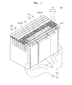
- FIG. 1 is a schematic diagram of a configuration of an ultrasound probe according to an exemplary embodiment of the present invention
- FIG. 2 is a diagram illustrating a method of manufacturing a backing layer of the ultrasound probe of FIG. 1 , which includes first and second electrodes, according to an exemplary embodiment of the present invention
- FIGS. 3A through 3I are diagrams for explaining a method of manufacturing the ultrasound probe of FIG. 1 by using the backing layer shown in FIG. 2 , according to an exemplary embodiment of the present invention
- FIGS. 4A through 4D illustrate a base piezoelectric element shown in FIG. 3E according to exemplary embodiments of the present invention.
- FIG. 5 is a block diagram of an ultrasound diagnostic apparatus including the ultrasound probe of FIG. 1 .
- an “object” may include a person or an animal, or a part of a person or an animal.
- the object may include organs such as the liver, the heart, the womb, the brain, a breast, and the abdomen, or a blood vessel.
- a “user” refers to a medical professional, such as a doctor, a nurse, a medical laboratory technologist, a medical imaging expert, and an engineer who repairs a medical apparatus, but the user is not limited thereto. Expressions such as “at least one of,” when preceding a list of elements, modify the entire list of elements and do not modify the individual elements of the list.
- FIG. 1 is a schematic diagram of a configuration of an ultrasound probe 100 according to an exemplary embodiment of the present invention.
- the ultrasound probe 100 includes a backing layer 110 having first and second surfaces S 1 and S 2 with different heights due to forming a groove 120 in the backing layer 110 , a first electrode 130 that is disposed inside the backing layer 110 and exposed on the first surface S 1 , a second electrode 140 that is disposed inside the backing layer 110 and exposed on the second surface S 2 , a third electrode 150 that is disposed in the groove 120 and contacts the first electrode 130 , a piezoelectric unit 160 that includes a piezoelectric layer 161 and is disposed on the third electrode 150 , and a fourth electrode 170 disposed on the backing layer 110 and the piezoelectric unit 160 .
- the ultrasound probe 100 may further include a matching layer 180 formed on the fourth electrode 170 .
- the backing layer 110 may absorb ultrasounds transmitted thereinto and has the groove 120 formed therein.
- the groove 120 may be formed in a top surface of the backing layer 110 so that the groove 120 has a shape corresponding to that of the piezoelectric unit 160 and is concave in the backing layer 110 .
- the backing layer 110 may have first and second surfaces S 1 and S 2 having different heights.
- the backing layer 110 may be formed of a material containing rubber with epoxy resin and tungsten powder added thereto.
- the backing layer 110 may be formed by joining together a plurality of sub-backing layers, e.g., first through third sub-backing layers 111 , 113 , and 115 .
- the second sub-backing layers 113 are disposed on either edge of the third sub-backing layer 115
- the first sub-backing layers 111 are respectively disposed on edges of the second sub-backing layers 113 .
- the second electrodes 140 may be disposed between the first and second sub-backing layers 111 and 113 , and the first electrode 130 may be disposed between the second and third sub-backing layers 113 and 115 .
- Each of the first and second electrodes 130 and 140 has one end exposed on a top of the backing layer 110 and the other end exposed on a bottom of the backing layer 110 . Therefore, the ends of the and second electrodes 130 and 140 on one side of each of the first and the second electrodes 130 and 140 are in contact with other electrodes disposed on the backing layer 110 , e.g., the third and fourth electrodes 150 and 170 , respectively.
- first and second electrodes 130 and 140 are electrically connected to a chip module substrate (not shown?) of the ultrasound probe 100 .
- a chip module substrate not shown
- the first and second electrodes 130 and 140 are disposed between the second sub-backing layer 113 and either the third or first sub-backing layer 115 or 111
- embodiments of the present invention are not limited thereto.
- the first and second electrodes 130 and 140 may be disposed on insulating layers, respectively, and the insulating layers having the first and second electrodes 130 and 140 thereon may be disposed between each of the first through third sub-backing layers 111 , 113 , and 115 .
- One of the first and second electrodes 130 and 140 may receive a driving signal from the chip module substrate while the other may receive a ground signal therefrom.
- the first and second electrodes 130 and 140 may receive a driving signal and a ground signal from the chip module substrate, respectively.
- the first and second electrodes 130 and 140 may also be called a signal electrode and a ground electrode, respectively.
- the first and second electrodes 130 and 140 are hereinafter referred to as a signal electrode and a ground electrode, respectively, but are not limited thereto.
- a ground signal and a driving signal may be applied to the first and second electrodes 130 and 140 , respectively.
- the first electrode 130 serving as a signal electrode may include a plurality of first electrode elements 132 and 134 that are separate from each other so that one of the first electrode elements 132 and 134 may contact one of a plurality of piezoelectric elements, as described below.
- the second electrode 140 serving as a ground electrode may include a plurality of second electrode elements ( 142 and 144 ?) that are separate from each other, and each second electrode element 142 or 144 may be formed of a single conductive material layer.
- each of the first and second electrodes 130 and 140 may include (two types of electrode elements 132 and 134 (or 142 and 144 ).
- the first electrode elements 132 and 134 are disposed on the left and right sides of the third sub-backing layer 115 , respectively, and in a staggered form. This staggered arrangement may decrease the size of a piezoelectric element.
- the second electrode 140 since the second electrode 140 includes the two second electrode elements 142 and 144 , one of the second electrode elements 142 and 144 may receive a ground signal even if the other electrode element suffers from a ground failure. Thus, a failure rate of the ultrasound probe 100 may be reduced.
- the first and second electrodes 130 and 140 each may include one type of electrode elements.
- At least one of the first and second electrodes 130 and 140 may be a flexible printed circuit board (PCB).
- PCB flexible printed circuit board
- the third electrode 150 is disposed in the groove 120 and contacts the first electrode 130 .
- the third electrode 150 may be a signal electrode as well.
- the third electrode 150 may include a plurality of third electrode elements 152 that are separate from each other. Since the third electrode 150 is formed using a deposition process such as sputtering, the third electrode 150 may be thin. For example, the third electrode 150 may have a thickness of about 7000 ⁇ .
- the piezoelectric unit 160 is disposed within the groove 120 and on the third electrode 150 .
- the piezoelectric unit 160 may also include a plurality of separate piezoelectric elements 162 that are in contact with the third electrode elements 152 , respectively.
- the piezoelectric elements 162 convert electrical signals into ultrasounds and vice versa while oscillating.
- the piezoelectric unit 160 may be made of a material that causes a piezoelectric phenomenon to occur.
- the material may include at least one of zinc oxide (ZnO), aluminum nitride (AlN), lead zirconate titanate (PbZrTiO 3 ; PZT), lead lanthanum zirconate titanate (PbLaZrTiO 3 ; PLZT), barium titanate (BaTiO 3 ; BT), lead titanate (PbTiO 3 ; PT), and lead magnesium niobate (Pb(Mg 1/3 Nb 2/3 )O 3 —PT (PMN—PT).
- the third electrode 150 and the piezoelectric unit 160 may be formed in the groove 120 by using a deposition process. Since the piezoelectric unit is formed by using a deposition method, the piezoelectric layer 161 may have a thickness of less than or equal to 200 ⁇ m.
- the piezoelectric unit 160 may only include the piezoelectric layer 161 made of a piezoelectric material. If the piezoelectric unit 160 only includes the piezoelectric layer 161 , a bottom surface and a top surface of the piezoelectric layer 161 may contact the third and fourth electrodes 150 and 170 , respectively, but are not limited thereto.
- the piezoelectric unit 160 may further include an auxiliary electrode (not shown) that contacts the bottom surface of the piezoelectric layer 161 .
- the auxiliary electrode may contact the third electrode 150 as well. In other words, by joining the auxiliary electrode directly with the third electrode 150 , a separation between the piezoelectric unit 160 and the third electrode 150 may be reduced, and accordingly, a failure rate of the ultrasound probe 100 may be reduced.
- the fourth electrode 170 is disposed on the backing layer 110 and the piezoelectric unit 160 and is electrically connected to the piezoelectric unit 160 and the second electrode 140 .
- the fourth electrode 170 may contact the piezoelectric unit 160 and the second electrode 140 for electrical connection.
- the fourth electrode 170 may include a plurality of fourth electrode elements 172 that are separate from one another.
- Each of the fourth electrode elements 172 is disposed on regions of the piezoelectric element 162 and the backing layer 110 and is electrically connected to the second electrode 140 .
- each of the fourth electrode elements 172 may contact the second electrode 140 for electrical connection.
- a surface of the piezoelectric unit 160 may be at the same level as the second surface S 2 of the backing layer 110 .
- the fourth electrode 170 may be formed by using a deposition process such as sputtering, vacuum evaporation, vapor deposition, plating, silk screen, printing. Since the fourth electrode 170 is formed using a deposition process, the fourth electrode 170 may be thin. For example, the fourth electrode 170 may have a thickness of about 7000 ⁇ .
- the first through fourth electrodes 130 , 140 , 150 , and 170 may be formed of conductive materials.
- the conductive materials may include metals, carbon nanostructures such as carbon nanotubes (CNTs) and graphene, various conductive polymers such as polypyrrole, polyaniline, polyacetylene, polythiophene, polyphnylene vinylene, polyphenylene sulfide, poly p-phenylene, and polyheterocycle vinylene, metal oxides such as indium tin oxide (ITO), aluminum zinc oxide (AZO), indium zinc oxide (IZO), tin oxide (SnO 2 ), or indium oxide (In 2 O 3 ), and thin-films with dispersed metal nanoparticles including Al, copper (Cu), gold (Au), and silver (Ag).
- ITO indium tin oxide
- AZO aluminum zinc oxide
- IZO indium zinc oxide
- SnO 2 tin oxide
- In 2 O 3 indium oxide
- the matching layer 180 may match an acoustic impedance of an ultrasound generated by the piezoelectric unit 160 to an acoustic impedance of an object.
- the matching layer 180 may gradually change the acoustic impedance of the ultrasound so that it is close to that of the object.
- the matching layer 180 may also include a plurality of matching elements 182 disposed on the fourth electrode elements 172 , respectively, but is not limited thereto.
- the matching layer 180 may be formed of a single layer or have a multi-layer structure. Since the matching layer 180 may also be formed using a deposition process, the matching layer 180 may have a thickness of less than or equal to 50 ⁇ m.
- the matching layer 180 may be formed by using a molding process and then a polishing process.
- the ultrasound probe 100 may further include an acoustic lens (not shown) for condensing ultrasounds.
- the acoustic lens is used to focus ultrasounds generated by the piezoelectric unit 160 .
- the acoustic lens may be formed of a material such as silicon rubber having acoustic impedance that is close to that of an object.
- the acoustic lens may have a convex or flat central portion.
- the acoustic lens may have various shapes according to design requirements.
- FIG. 2 is a diagram illustrating a method of manufacturing the backing layer 110 in the ultrasound probe 100 of FIG. 1 , which includes the first and second electrodes 130 and 140 , according to an exemplary embodiment of the present invention.
- the second electrode 140 may be formed on a side of the first sub-backing layer 111 by depositing a conductive material.
- the second electrode 140 may be formed as a pattern by partitioning the conductive material into the plurality of second electrode elements 142 and 144 , or as a single electrode layer.
- the first electrode 130 may be formed on a side of the second sub-backing layer 113 .
- the first electrode 130 may be patterned into the plurality of first electrode elements 132 and 134 by depositing a conductive material and then patterning the same. Thereafter, the second sub-backing layer 113 with the first electrode 130 formed on the side thereof may be joined to a side of the third sub-backing layer 115 , and the first sub-backing layer 111 having the second electrode 140 on the side thereof may be bonded to a side of the second sub-backing layer 113 .
- the first through third sub-backing layers 111 , 113 , and 115 may be joined to one another simultaneously or in a different order than described above.
- Empty spaces between the second sub-backing layer 113 and either the first or third sub-backing layer 111 or 115 may be filled with backing materials during joining of the first through third sub-backing layers 111 , 113 , and 115 .
- the first and second electrodes 130 and 140 may be flexible PCBs.
- FIGS. 3A through 3I are reference diagrams for explaining a method of manufacturing the ultrasound probe 100 of FIG. 1 by using the backing layer 110 shown in FIG. 2 , according to an exemplary embodiment of the present invention.
- FIG. 3A illustrates the result of joining the first through third sub-backing layers 111 , 113 , and 115 shown in FIG. 2 .
- the first through third sub-backing layers 111 , 113 , and 115 may be joined together to form the backing layer 110 including the first and second electrodes 130 and 140
- the groove 120 is formed in an upper portion of the backing layer 110 by removing a portion of the second sub-backing layer 113 and the third sub-backing layer 115 .
- the removal process may include an etching or polishing process.
- the second sub-backing layer 113 may have a stepped surface.
- the backing layer 110 may have first and third surfaces S 1 and S 3 with different heights.
- the first and second electrodes 130 and 140 may be exposed on the first and third surfaces S 1 and S 3 , respectively.
- a conductive material 151 may be formed in the groove 120 by using sputtering.
- the conductive material 151 may include metals, carbon nanostructures such as CNTs and graphene, various conductive polymers such as polypyrrole, polyaniline, polyacetylene, polythiophene, polyphnylene vinylene, polyphenylene sulfide, poly p-phenylene, and polyheterocycle vinylene, metal oxides such as ITO, AZO, IZO, SnO 2 , or In 2 O 3 , and thin-films with dispersed metal nanoparticles including Al, Cu, Au, and Ag.
- the third electrode 150 may be formed by removing a part of the conductive material 151 formed along sidewalls of the groove 120 .
- the third electrode 150 may be formed by etching or cutting the part of the conductive material 151 .
- the third electrode 150 may be formed on a bottom surface of the groove 120 and electrically connected to the first electrode 130 .
- the third electrode 150 may contact the first electrode 130 for electrical connection.
- a base piezoelectric unit 160 a may be formed in the groove 120 and include the piezoelectric layer 161 .
- the base piezoelectric unit 160 a may further include first and second auxiliary electrodes ( 163 and 164 in FIG. 4D ) disposed on top and bottom surfaces of the piezoelectric layer 161 , respectively.
- FIGS. 4A through 4D illustrate the base piezoelectric unit 160 a shown in FIG. 3E according to exemplary embodiments of the present invention.
- the base piezoelectric unit 160 a may only include the piezoelectric layer 161 , but is not limited thereto. As shown in FIG. 4B , the base piezoelectric unit 160 a may further include the first auxiliary electrode 163 disposed on the top surface of the piezoelectric layer 161 . Referring to FIG. 4C , the base piezoelectric unit 160 a may further include the second auxiliary electrode 164 disposed on the bottom surface of the piezoelectric layer 161 . Referring to FIG. 4D , the base piezoelectric unit 160 a may further include the first and second auxiliary electrodes 163 and 164 disposed on the top and bottom surfaces of the piezoelectric layer 161 , respectively. Referring back to FIG. 3E , the base piezoelectric unit 160 a , including the piezoelectric layer 161 and the first and second auxiliary electrodes 163 and 164 , is formed in the groove 120 .
- an upper portion of the base piezoelectric unit 160 a is removed to form the piezoelectric unit 160 .
- a surface of the piezoelectric unit 160 is at the same level as a second surface S 2 of the backing layer 110 .
- an upper portion of the piezoelectric layer 161 may be removed as well. Since the piezoelectric unit 160 is formed by removing part of the base piezoelectric unit 160 a , a thickness of the piezoelectric layer 161 may be adjusted regardless of a depth of the groove 120 .
- the upper portion of the base piezoelectric unit 160 a may be removed using an etching or polishing process.
- the resulting structure may have equal height at a time so that the fourth electrode 170 is formed thereon.
- the fourth electrode 170 may then be formed on the second surface S 2 of the backing layer 110 and the piezoelectric unit 160 .
- the fourth electrode 170 may also be formed by depositing a conductive material thereon.
- the fourth electrode 170 may contact the piezoelectric unit 160 as well as the second electrode 140 exposed on the second surface S 2 .
- the fourth electrode 170 may ground a top surface of the piezoelectric unit 160 in response to a ground signal applied through the second electrode 140 .
- the matching layer 180 may be formed on the fourth electrode 170 by using a deposition process such as sputtering, vacuum evaporation, vapor deposition, plating, silk screen, printing. Since the matching layer 180 is formed by using a deposition process, the matching layer 180 may be a thin layer having a thickness of less than or equal to 50 ⁇ m. However, embodiments of the present invention are not limited thereto.
- the matching layer 180 may also be formed by using a molding process. Then, as shown in FIG. 3I , the matching layer 180 may be planarized by using an etching or polishing process.
- the matching layer 180 , the fourth electrode 170 , the piezoelectric unit 160 , the third electrode 150 , and a portion of the backing layer 110 may be diced to form the plurality of matching elements 182 , the plurality of fourth electrode elements 172 , the plurality of piezoelectric elements 162 , and the plurality of third electrode elements 152 , as shown in FIG. 1 .
- an acoustic lens may be stacked on the matching elements 182 .
- FIG. 5 is a block diagram of an ultrasound diagnostic apparatus 200 including the ultrasound probe 100 of FIG. 1 .
- the ultrasound diagnostic apparatus 200 includes the ultrasound probe 100 for transmitting or receiving ultrasounds, a signal processor 220 that processes a signal applied by the ultrasound probe 100 to generate an image, a display 230 for displaying an image, a user interface 240 for receiving a user command, a storage 250 for storing various types of information, and a controller 260 for controlling overall operations of the ultrasound diagnostic apparatus 200 .
- the ultrasound probe 100 is configured to transmit an ultrasound to an object and receive an ultrasound echo signal reflected from the object, which will be described in more detail below.
- the signal processor 220 may process ultrasound data generated by the ultrasound probe 100 and generate an ultrasound image.
- the ultrasound image may be at least one of a brightness (B) mode image indicating the intensity of an ultrasound echo signal reflected from an object as brightness, a Doppler mode image showing a moving object as a spectrum by using a Doppler effect, a motion (M) mode image showing movement of an object at a predetermined position over time, an elasticity mode image indicating a difference between deformations of an object when compression is applied and when no compression is applied, and a color (C) mode image representing the speed of a moving object in color by using a Doppler effect. Since an ultrasound image may be generated by using a currently implementable method, a detailed description thereof is omitted herein.
- the ultrasound image may include images of all dimensions, such as one-dimensional (1D), two-dimensional (2D), three-dimensional (3D), and four-dimensional (4D) images.
- the display 230 displays information that is processed by the ultrasound diagnostic apparatus 200 .
- the display 230 may display an ultrasound image generated by the signal processor 220 as well as a graphical user interface (GUI) for requesting a user input.
- GUI graphical user interface
- the display 230 may include at least one of a liquid crystal display (LCD), a thin film transistor-LCD (TFT-LCD), an organic light-emitting diode (OLED) display, a flexible display, a 3D display, and an electrophoretic display.
- the ultrasound diagnostic apparatus 200 may include two or more displays according to embodiments of the present invention.
- the user interface 240 is a means via which a user inputs data for controlling the ultrasound diagnostic apparatus 200 .
- the user interlace 240 may include a keypad, a mouse, a touch panel, and a trackball.
- the user interface 240 is not limited thereto and may further include various other input elements such as a jog wheel, jog switch, etc.
- the touch panel may detect both a real touch where a pointer actually touches a screen and a proximity touch where the pointer approaches the screen while being separate from the screen by less than a predetermined distance.
- the term ‘pointer’ means a tool for touching a particular portion on or near the touch panel. Examples of the pointer may include a stylus pen and a body part such as fingers.
- the touch panel may be realized as a touch screen that forms a layer structure with the display 230 .
- the touch screen may be implemented as various types such as capacitive overlay, resistive overlay, infrared beam, surface acoustic wave, integral strain gauge, and piezoelectric touch screens.
- the touch screen is very useful because it functions as both the display 230 and the user interface 240 .
- various sensors may be disposed within or near the touch panel so as to sense a touch.
- a tactile sensor is an example of the sensors for sensing a touch.
- the tactile sensor is used to sense a touch of a particular object to the same or greater degree than the degree to which a human can sense the touch.
- the tactile sensor may detect various types of information including the roughness of a contact surface, the hardness of an object to be touched, and the temperature of a point to be touched.
- a proximity sensor is another example of the sensors for sensing a touch.
- the proximity sensor means a sensor that senses the presence of an object that is approaching or is located near a predetermined detection surface by using the force of an electromagnetic field or infrared light without any mechanical contact.
- Examples of the proximity sensor include a transmissive photoelectric sensor, a direct reflective photoelectric sensor, a mirror reflective photoelectric sensor, a high-frequency oscillation proximity sensor, a capacitive proximity sensor, a magnetic proximity sensor, and an infrared proximity sensor.
- the storage 250 stores various types of information that are processed by the ultrasound diagnostic apparatus 200 .
- the storage 250 may store medical data related to diagnosis of an object, such as images, and algorithms or programs that are executed in the ultrasound diagnostic apparatus 200 .
- the storage 250 may include at least one storage medium from among a flash memory-type storage medium, a hard disk-type storage medium, a multimedia card micro-type storage medium, card-type memories (e.g., an SD memory, an XD memory, and the like), Random Access Memory (RAM), Static Random Access Memory (SRAM), Read-Only Memory (ROM), Electrically Erasable Programmable ROM (EEPROM), PROM, magnetic memory, a magnetic disc, and an optical disc.
- the ultrasound diagnostic apparatus 200 may utilize a web storage or a cloud server that functions as the storage 250 online.
- the controller 260 controls the overall operations of the ultrasound diagnostic apparatus 200 .
- the controller 260 may control operations of the ultrasound probe 100 , the signal processor 220 , and the display 230 .
- the controller 260 may control the signal processor 220 to generate an image by using a user command received via the user interface 240 or programs stored in the storage 250 .
- the controller 260 may also control the display 230 to display the image generated by the signal processor 220 .
- a failure rate may be reduced during the manufacture of an ultrasound probe.
Priority Applications (1)
| Application Number | Priority Date | Filing Date | Title |
|---|---|---|---|
| US15/804,814 US10199563B2 (en) | 2014-03-04 | 2017-11-06 | Ultrasound probe |
Applications Claiming Priority (2)
| Application Number | Priority Date | Filing Date | Title |
|---|---|---|---|
| KR10-2014-0025678 | 2014-03-04 | ||
| KR1020140025678A KR102205505B1 (ko) | 2014-03-04 | 2014-03-04 | 초음파 프로브의 제조 방법 및 그 초음파 프로브 |
Related Child Applications (1)
| Application Number | Title | Priority Date | Filing Date |
|---|---|---|---|
| US15/804,814 Division US10199563B2 (en) | 2014-03-04 | 2017-11-06 | Ultrasound probe |
Publications (2)
| Publication Number | Publication Date |
|---|---|
| US20150250452A1 US20150250452A1 (en) | 2015-09-10 |
| US9812635B2 true US9812635B2 (en) | 2017-11-07 |
Family
ID=52574017
Family Applications (2)
| Application Number | Title | Priority Date | Filing Date |
|---|---|---|---|
| US14/607,884 Active 2035-08-08 US9812635B2 (en) | 2014-03-04 | 2015-01-28 | Method of manufacturing ultrasound probe |
| US15/804,814 Active US10199563B2 (en) | 2014-03-04 | 2017-11-06 | Ultrasound probe |
Family Applications After (1)
| Application Number | Title | Priority Date | Filing Date |
|---|---|---|---|
| US15/804,814 Active US10199563B2 (en) | 2014-03-04 | 2017-11-06 | Ultrasound probe |
Country Status (4)
| Country | Link |
|---|---|
| US (2) | US9812635B2 (ko) |
| EP (1) | EP2915594B1 (ko) |
| KR (1) | KR102205505B1 (ko) |
| CN (1) | CN104887264B (ko) |
Cited By (1)
| Publication number | Priority date | Publication date | Assignee | Title |
|---|---|---|---|---|
| US20180021815A1 (en) * | 2015-05-22 | 2018-01-25 | Halliburton Energy Services, Inc. | Ultrasonic Transducers with Piezoelectric Material Embedded in Backing |
Families Citing this family (12)
| Publication number | Priority date | Publication date | Assignee | Title |
|---|---|---|---|---|
| CN105232090B (zh) * | 2015-10-28 | 2017-08-25 | 上海爱声生物医疗科技有限公司 | 一种性能优化的高频超声换能器及其制作方法 |
| KR102227329B1 (ko) * | 2016-07-26 | 2021-03-12 | 지멘스 메디컬 솔루션즈 유에스에이, 인크. | 초음파 트랜스듀서 및 그 제조 방법 |
| US11039814B2 (en) * | 2016-12-04 | 2021-06-22 | Exo Imaging, Inc. | Imaging devices having piezoelectric transducers |
| KR20180068586A (ko) * | 2016-12-14 | 2018-06-22 | 삼성메디슨 주식회사 | 초음파 진단 장치용 프로브 |
| US10656007B2 (en) | 2018-04-11 | 2020-05-19 | Exo Imaging Inc. | Asymmetrical ultrasound transducer array |
| US10648852B2 (en) | 2018-04-11 | 2020-05-12 | Exo Imaging Inc. | Imaging devices having piezoelectric transceivers |
| US11583259B2 (en) * | 2018-12-19 | 2023-02-21 | Fujifilm Sonosite, Inc. | Thermal conductive layer for transducer face temperature reduction |
| AU2020344610A1 (en) | 2019-09-12 | 2022-04-07 | Exo Imaging, Inc. | Increased MUT coupling efficiency and bandwidth via edge groove, virtual pivots, and free boundaries |
| US11951512B2 (en) | 2021-03-31 | 2024-04-09 | Exo Imaging, Inc. | Imaging devices having piezoelectric transceivers with harmonic characteristics |
| US11819881B2 (en) | 2021-03-31 | 2023-11-21 | Exo Imaging, Inc. | Imaging devices having piezoelectric transceivers with harmonic characteristics |
| CN113333261B (zh) * | 2021-06-18 | 2022-07-08 | 深圳先进技术研究院 | 一种高频阵列换能器 |
| KR102608457B1 (ko) * | 2022-10-17 | 2023-12-01 | 주식회사 소닉랩 | 초음파 진단용 프로브 및 그 제조방법 |
Citations (12)
| Publication number | Priority date | Publication date | Assignee | Title |
|---|---|---|---|---|
| US5857974A (en) | 1997-01-08 | 1999-01-12 | Endosonics Corporation | High resolution intravascular ultrasound transducer assembly having a flexible substrate |
| US6036647A (en) * | 1998-07-31 | 2000-03-14 | Scimed Life Systems, Inc. | PZT off-aperture bonding technique |
| JP2006095178A (ja) | 2004-09-30 | 2006-04-13 | Olympus Corp | 超音波振動子アレイ |
| US20080033298A1 (en) * | 2006-08-02 | 2008-02-07 | Takeshi Habu | Ultrasonic probe |
| US20080312537A1 (en) | 2007-06-12 | 2008-12-18 | Fujifilm Corporation | Composite piezoelectric material, ultrasonic probe, ultrasonic endoscope, and ultrasonic diagnostic apparatus |
| US20090204006A1 (en) | 2004-09-24 | 2009-08-13 | Katsuhiro Wakabayashi | Ultrasonic transducer, ultrasonic transducer array and ultrasonic endoscope system |
| US20100241004A1 (en) * | 2009-03-18 | 2010-09-23 | Jung Jin Woo | Probe For Ultrasonic Diagnostic Apparatus And Method Of Manufacturing The Same |
| US20100241003A1 (en) | 2009-03-18 | 2010-09-23 | Jung Jin Woo | Probe For Ultrasonic Diagnostic Apparatus And Method Of Manufacturing The Same |
| US7834522B2 (en) | 2007-08-03 | 2010-11-16 | Mr Holdings (Hk) Limited | Diagnostic ultrasound transducer |
| JP4703416B2 (ja) | 2006-01-27 | 2011-06-15 | 株式会社東芝 | 超音波トランスデューサ |
| JP2012182758A (ja) * | 2011-03-03 | 2012-09-20 | Konica Minolta Medical & Graphic Inc | 超音波探触子の製造方法 |
| US20140154795A1 (en) | 2012-03-15 | 2014-06-05 | Flodesign Sonics, Inc. | Bioreactor using acoustic standing waves |
Family Cites Families (6)
| Publication number | Priority date | Publication date | Assignee | Title |
|---|---|---|---|---|
| JP4253334B2 (ja) * | 2006-07-12 | 2009-04-08 | 株式会社東芝 | 2次元アレイ型超音波プローブ |
| KR101112658B1 (ko) * | 2008-11-19 | 2012-02-15 | 삼성메디슨 주식회사 | 초음파 진단장치용 프로브 및 그 제조방법 |
| KR101196214B1 (ko) * | 2010-09-06 | 2012-11-05 | 삼성메디슨 주식회사 | 초음파 진단장치용 프로브 |
| KR101435011B1 (ko) * | 2012-02-20 | 2014-08-27 | 삼성메디슨 주식회사 | 초음파 프로브 및 그 제조방법 |
| CN102608221B (zh) * | 2012-03-02 | 2014-01-08 | 中国航空工业集团公司北京航空制造工程研究所 | 用于复合材料检测的超声探头的换能传感器 |
| JP5746082B2 (ja) * | 2012-03-30 | 2015-07-08 | 富士フイルム株式会社 | 超音波探触子および信号線の接続方法 |
-
2014
- 2014-03-04 KR KR1020140025678A patent/KR102205505B1/ko active IP Right Grant
-
2015
- 2015-01-28 US US14/607,884 patent/US9812635B2/en active Active
- 2015-01-30 EP EP15153222.3A patent/EP2915594B1/en active Active
- 2015-03-04 CN CN201510096643.5A patent/CN104887264B/zh active Active
-
2017
- 2017-11-06 US US15/804,814 patent/US10199563B2/en active Active
Patent Citations (14)
| Publication number | Priority date | Publication date | Assignee | Title |
|---|---|---|---|---|
| US5857974A (en) | 1997-01-08 | 1999-01-12 | Endosonics Corporation | High resolution intravascular ultrasound transducer assembly having a flexible substrate |
| US6036647A (en) * | 1998-07-31 | 2000-03-14 | Scimed Life Systems, Inc. | PZT off-aperture bonding technique |
| US20090204006A1 (en) | 2004-09-24 | 2009-08-13 | Katsuhiro Wakabayashi | Ultrasonic transducer, ultrasonic transducer array and ultrasonic endoscope system |
| JP2006095178A (ja) | 2004-09-30 | 2006-04-13 | Olympus Corp | 超音波振動子アレイ |
| JP4703416B2 (ja) | 2006-01-27 | 2011-06-15 | 株式会社東芝 | 超音波トランスデューサ |
| US20080033298A1 (en) * | 2006-08-02 | 2008-02-07 | Takeshi Habu | Ultrasonic probe |
| US20080312537A1 (en) | 2007-06-12 | 2008-12-18 | Fujifilm Corporation | Composite piezoelectric material, ultrasonic probe, ultrasonic endoscope, and ultrasonic diagnostic apparatus |
| US7834522B2 (en) | 2007-08-03 | 2010-11-16 | Mr Holdings (Hk) Limited | Diagnostic ultrasound transducer |
| US20100241004A1 (en) * | 2009-03-18 | 2010-09-23 | Jung Jin Woo | Probe For Ultrasonic Diagnostic Apparatus And Method Of Manufacturing The Same |
| KR20100104535A (ko) | 2009-03-18 | 2010-09-29 | 주식회사 메디슨 | 초음파 진단장치용 프로브 및 그 제조방법 |
| KR20100104534A (ko) | 2009-03-18 | 2010-09-29 | 주식회사 메디슨 | 초음파 진단장치용 프로브 및 그 제조방법 |
| US20100241003A1 (en) | 2009-03-18 | 2010-09-23 | Jung Jin Woo | Probe For Ultrasonic Diagnostic Apparatus And Method Of Manufacturing The Same |
| JP2012182758A (ja) * | 2011-03-03 | 2012-09-20 | Konica Minolta Medical & Graphic Inc | 超音波探触子の製造方法 |
| US20140154795A1 (en) | 2012-03-15 | 2014-06-05 | Flodesign Sonics, Inc. | Bioreactor using acoustic standing waves |
Non-Patent Citations (1)
| Title |
|---|
| Extended European Search Report issued in Application No. 15153222.3 dated Aug. 11, 2015. |
Cited By (2)
| Publication number | Priority date | Publication date | Assignee | Title |
|---|---|---|---|---|
| US20180021815A1 (en) * | 2015-05-22 | 2018-01-25 | Halliburton Energy Services, Inc. | Ultrasonic Transducers with Piezoelectric Material Embedded in Backing |
| US11117166B2 (en) * | 2015-05-22 | 2021-09-14 | Halliburton Energy Services, Inc. | Ultrasonic transducers with piezoelectric material embedded in backing |
Also Published As
| Publication number | Publication date |
|---|---|
| KR20150103959A (ko) | 2015-09-14 |
| CN104887264B (zh) | 2019-09-24 |
| US10199563B2 (en) | 2019-02-05 |
| KR102205505B1 (ko) | 2021-01-20 |
| EP2915594A1 (en) | 2015-09-09 |
| US20180062069A1 (en) | 2018-03-01 |
| US20150250452A1 (en) | 2015-09-10 |
| CN104887264A (zh) | 2015-09-09 |
| EP2915594B1 (en) | 2021-06-02 |
Similar Documents
| Publication | Publication Date | Title |
|---|---|---|
| US10199563B2 (en) | Ultrasound probe | |
| KR102433315B1 (ko) | 초음파 트랜스듀서가 임베디드된 유기 발광 다이오드 패널 및 이를 포함하는 표시 장치 | |
| KR102395636B1 (ko) | 압전 패널 스피커 및 이를 포함하는 전자 기기 | |
| US9465972B2 (en) | Fingerprint sensor and electronic device including the same | |
| US11024796B2 (en) | Method of manufacturing an ultrasonic probe | |
| KR101880670B1 (ko) | 압력 센서를 구비하는 전자기기 | |
| US10441974B2 (en) | Ultrasonic transducer and ultrasonic probe including the same | |
| TWI675333B (zh) | 指紋識別裝置及電子裝置 | |
| US20200160018A1 (en) | Ultrasonic biometric sensor with transmit and receive side beamforming | |
| US10074798B2 (en) | Method of manufacturing ultrasonic probe | |
| EP2839887B1 (en) | Acoustic probe and method of manufacturing the same | |
| CN109492456A (zh) | 超声波传感器及电子装置 | |
| US20160199031A1 (en) | Matching member and ultrasound probe including the same | |
| US20150033195A1 (en) | Hardware device, user control apparatus for the same, medical apparatus including the same, and method of operating medical apparatus | |
| US20150196276A1 (en) | Ultrasonic probe and method of manufacturing the same | |
| US20170202539A1 (en) | Ultrasonic probe and method of manufacturing the same | |
| US11475694B2 (en) | Touch recognition device, display device and manufacturing method thereof | |
| KR102249526B1 (ko) | 초음파 프로브의 제조 방법 및 그 장치 | |
| JP2018074529A (ja) | 超音波探触子、超音波診断装置及び超音波探触子の製造方法 | |
| KR102607016B1 (ko) | 초음파 프로브 | |
| EP2902116A2 (en) | Ultrasonic probe and method of manufacturing the same | |
| JP2018132853A (ja) | 触覚呈示装置 |
Legal Events
| Date | Code | Title | Description |
|---|---|---|---|
| AS | Assignment |
Owner name: SAMSUNG MEDISON CO., LTD, KOREA, REPUBLIC OF Free format text: ASSIGNMENT OF ASSIGNORS INTEREST;ASSIGNORS:JIN, GIL-JU;PARK, JUNG-LIM;SIGNING DATES FROM 20141212 TO 20141222;REEL/FRAME:034834/0630 Owner name: SAMSUNG MEDISON CO., LTD., KOREA, REPUBLIC OF Free format text: ASSIGNMENT OF ASSIGNORS INTEREST;ASSIGNORS:JIN, GIL-JU;PARK, JUNG-LIM;SIGNING DATES FROM 20141212 TO 20141222;REEL/FRAME:034834/0662 |
|
| STCF | Information on status: patent grant |
Free format text: PATENTED CASE |
|
| MAFP | Maintenance fee payment |
Free format text: PAYMENT OF MAINTENANCE FEE, 4TH YEAR, LARGE ENTITY (ORIGINAL EVENT CODE: M1551); ENTITY STATUS OF PATENT OWNER: LARGE ENTITY Year of fee payment: 4 |