US9806980B2 - Methods, systems, and computer readable media for precise measurement of switching latency of packet switching devices - Google Patents
Methods, systems, and computer readable media for precise measurement of switching latency of packet switching devices Download PDFInfo
- Publication number
- US9806980B2 US9806980B2 US14/228,101 US201414228101A US9806980B2 US 9806980 B2 US9806980 B2 US 9806980B2 US 201414228101 A US201414228101 A US 201414228101A US 9806980 B2 US9806980 B2 US 9806980B2
- Authority
- US
- United States
- Prior art keywords
- under test
- device under
- latency
- virtual lane
- backlog
- Prior art date
- Legal status (The legal status is an assumption and is not a legal conclusion. Google has not performed a legal analysis and makes no representation as to the accuracy of the status listed.)
- Active, expires
Links
- 238000000034 method Methods 0.000 title claims abstract description 32
- 238000005259 measurement Methods 0.000 title claims abstract description 14
- 238000012360 testing method Methods 0.000 claims abstract description 200
- 239000003550 marker Substances 0.000 claims abstract description 70
- 230000005540 biological transmission Effects 0.000 claims description 63
- 238000003780 insertion Methods 0.000 claims description 10
- 230000037431 insertion Effects 0.000 claims description 10
- 230000007423 decrease Effects 0.000 claims description 6
- 238000011084 recovery Methods 0.000 claims description 6
- 230000003139 buffering effect Effects 0.000 description 8
- 238000010586 diagram Methods 0.000 description 7
- 230000001360 synchronised effect Effects 0.000 description 7
- 239000000872 buffer Substances 0.000 description 4
- 230000003247 decreasing effect Effects 0.000 description 3
- 230000001934 delay Effects 0.000 description 2
- 238000005516 engineering process Methods 0.000 description 2
- 230000007246 mechanism Effects 0.000 description 2
- 230000002860 competitive effect Effects 0.000 description 1
- 230000003111 delayed effect Effects 0.000 description 1
- 238000001514 detection method Methods 0.000 description 1
- 230000000694 effects Effects 0.000 description 1
- 230000000737 periodic effect Effects 0.000 description 1
Images


Classifications
-
- H—ELECTRICITY
- H04—ELECTRIC COMMUNICATION TECHNIQUE
- H04L—TRANSMISSION OF DIGITAL INFORMATION, e.g. TELEGRAPHIC COMMUNICATION
- H04L43/00—Arrangements for monitoring or testing data switching networks
- H04L43/50—Testing arrangements
-
- H—ELECTRICITY
- H04—ELECTRIC COMMUNICATION TECHNIQUE
- H04L—TRANSMISSION OF DIGITAL INFORMATION, e.g. TELEGRAPHIC COMMUNICATION
- H04L43/00—Arrangements for monitoring or testing data switching networks
- H04L43/08—Monitoring or testing based on specific metrics, e.g. QoS, energy consumption or environmental parameters
- H04L43/0852—Delays
- H04L43/0864—Round trip delays
Definitions
- the subject matter described herein relates to testing network devices. More particularly, the subject matter described herein relates to methods, systems, and computer readable media for precise measurement of switching latency of packet switching devices.
- the switching latency of packet switching equipment is a key competitive product feature.
- Ethernet switch vendors currently advertise latencies on the order of nanoseconds. Because switching latency is an important product feature, switch manufacturers require a mechanism to accurately measure switching latency of their devices.
- the switching latency of a switch is a measure of how long it takes the switch to switch a packet from an ingress port of the switch to an egress port of the switch.
- a switch manufacturer may test the latency of a device, such as an Ethernet switch, by transmitting packets to the switch, determining when the packets are received from the switch, and calculating the difference between packet transmit and receive times.
- the average latency value, median latency value, mode latency or other statistical measure of latency derived from the tests may be reported or advertised as a product feature.
- the switching latency of a switch may increase beyond the advertised or rated value. Increases in switching latency beyond the advertised or rated latency value may be caused by improper buffering by the switch due to overloading of resources within the switch. However, another cause of switching latency that is not caused by improper buffering is buffering due to transmission of virtual lane markers or identifiers. Virtual lane markers are transmitted by packet switching devices to identify the lane with which the group of packets is associated. In 100 gigabit Ethernet, a compliant device is required to transmit a virtual lane marker or identifier of 160 bits every 207 microseconds.
- a test device transmits a packet to a device under test, and the packet is received when the device under test is required to send a virtual lane marker, the measured latency of the device under test will increase even though the increase in latency is not caused by improper buffering by the device under test. It is desirable to account for the effect of virtual lane marker transmission on device latency. Accordingly, there exists a need for improved methods, systems, and computer readable media for precise measurement of switching latency of packet switching devices.
- One method includes steps implemented in a network equipment test device including at least one processor.
- the method includes transmitting frames to a device under test.
- the method further includes receiving one of the transmitted frames from the device under test.
- the method further includes determining a measured latency of the device under test based on a difference between a time that the one frame was transmitted to the device under test and a time that the one frame was received from the device under test.
- the method further includes determining an indication of backlog latency of the device under test caused by the device under test inserting a virtual lane marker in traffic transmitted to the network equipment and reporting the indication of the backlog latency.
- the term “virtual lane marker” refers to a packet that is periodically inserted into a sequence of packets to allow lane identification and de-skewing by a receiver of the packets.
- the term “virtual lane marker” is intended to include, but not be limited to PCS lane identifiers.
- processor includes a device that is implemented at least partially in hardware.
- packet and “frame” are used interchangeably herein to refer to discrete units of digitized data.
- packet switching device refers to a device, such as an Ethernet switch, that switches packets between ingress and egress ports.
- the subject matter described herein may be implemented in hardware alone or in combination with software and/or firmware.
- the terms “function”, “node” or “module” as used herein refer to hardware, which may also include software and/or firmware components, for implementing the feature being described.
- the subject matter described herein may be implemented using a non-transitory computer readable medium having stored thereon computer executable instructions that when executed by the processor of a computer control the computer to perform steps.
- Exemplary computer readable media suitable for implementing the subject matter described herein include non-transitory computer-readable media, such as disk memory devices, chip memory devices, programmable logic devices, and application specific integrated circuits.
- a computer readable medium that implements the subject matter described herein may be located on a single device or computing platform or may be distributed across multiple devices or computing platforms.
- FIG. 1 is a block diagram illustrating an exemplary system for precise measurement of switching latency of a packet switching device according to an embodiment of the subject matter described herein;
- FIG. 2 is a diagram illustrating virtual lane data distribution that may be implemented by a network equipment test device and/or a device under test according to an embodiment of the subject matter described herein;
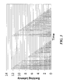
- FIG. 3 is a graph illustrating backlog latency resulting from virtual lane marker transmission that may be quantified and reported by a network equipment test device according to an embodiment of the subject matter described herein;
- FIG. 4 is a flow chart illustrating an exemplary process for precise measurement of switching latency of a packet switching device according to an embodiment of the subject matter described herein;
- FIG. 5 is a block diagram illustrating receive clock synchronization functionality of a network equipment test device according to an embodiment of the subject matter described herein;
- FIGS. 6A and 6B are block diagrams illustrating virtual lane marker synchronization by a network equipment test device according to an embodiment of the subject matter described herein.
- FIG. 1 is a block diagram illustrating an exemplary system for precise measurement of switching latency of packet switching devices according to an embodiment of the subject matter described herein.
- the system may include a network equipment test device 100 that transmits packets to and receives packets from a device under test 102 (DUT).
- Network equipment test device 100 includes traffic generators 104 that generate streams of packets or frames to be transmitted to device under test 102 .
- each traffic generator 104 may generate streams of 40 gigabit traffic, 100 gigabit Ethernet traffic, or any other speed/protocol combination where virtual lane markers may interrupt transmission of packets.
- the traffic generated by traffic generator 104 includes test packets to be transmitted to device under test 102 .
- Device under test 102 may be a switch, such as a 10G or 40G Ethernet switch.
- Both test device 100 and device under test 102 include transmit and receive modules 106 and 108 , which in the illustrated example are physical coding sublayer (PCS) transmit and receive modules.
- PCS physical coding sublayer
- Each PCS transmit module 106 is responsible for breaking streams of packets into virtual lanes and inserting virtual lane markers in the virtual lane to allow deskewing by the receiver.
- Each PCS receive module 108 performs deskewing using the virtual lane markers.
- FIG. 2 is a block diagram illustrating virtual lane data distribution that may be performed by PCS transmit modules 106 .
- each PCS transmit module 106 may receive as input an aggregate stream of 64/66 bit words and divide the stream into virtual lanes.
- Each virtual lane includes a virtual lane marker that is periodically transmitted to allow identification and deskewing of virtual lanes by PCS receive modules 108 .
- the virtual lane markers are inserted once every 16,384 clocks. Because the same resources are used for transmission of data and virtual lane markers, the transmission of virtual lane markers will delay transmission of data if there is data to be transmitted at the same time as a virtual lane marker.
- the virtual lane marker For 100 gigabit Ethernet, the virtual lane marker is 8 bytes and must be transmitted for each of 20 PCS or virtual lanes, resulting in 160 bytes.
- the device under test may have to delay transmission of the packet back to the network equipment test device by at worst one virtual lane marker (12.8 nanoseconds) due to the fixed and periodic insertion of the virtual lane marker. Because of this absolute best-case latency measurement, without the subject matter described herein, the best-case latency that can be measured is between 0 and 12.8 nanoseconds. And it is not possible to distinguish incorrectly buffered packets and the fact that the device under test is adhering to virtual lane marker requirements.
- PCS transmit module 106 associated with port 1 110 of network equipment test device 100 transmits test data to port 1 112 of device under test 102 .
- the test data is received by packet forwarding hardware 114 of device under test 102 , which determines that the test data should be forwarded to egress port 3 116 of device under test 102 and forwards the test data to port 3 116 .
- PCS transmit module 106 associated with port 3 116 transmits a virtual lane marker to network equipment test device 100 .
- test data is buffered, and the transmission of the test data from port 3 116 is delayed. Packets that need to be forwarded from port 3 116 will experience increased latency until the buffer is drained. It is desirable that network equipment test device 100 detect and quantify this latency.
- network equipment test device 100 includes latency calculation module 118 associated with each port.
- Latency calculation module 118 calculates latency experienced by Ethernet frames transmitted to and returned from a device under test.
- each latency calculation module 118 may calculate a measured latency based on a difference between a time that a frame is transmitted to device under test 102 and the time that the frame is received from device under test 102 . If a virtual lane marker is transmitted by device under test 102 during this interval, the measured latency will include latency caused by the virtual lane marker transmission.
- latency calculation module 118 may determine a backlog latency caused by device under test 102 inserting a virtual lane marker in traffic transmitted to network equipment test device 100 .
- a virtual lane marker When a virtual lane marker is inserted, it creates a temporary backlog in device under test 102 of 128 bytes of data. This backlog of data is drained by device under test 102 by shrinking the inter-packet gap or inter-frame gap of subsequent packets, for example, from sixteen to eight bytes. Until the 128 bytes of buffered data are drained, packets transitioning the device under test will have increased latency. This creates a backlog latency or latency offset between peaks of 209.7 microseconds, which is the interval between virtual lane marker transmissions.
- latency calculation modules 118 are associated with each port of network equipment test device 100 , the subject matter described herein is not limited to such an embodiment. In an alternate embodiment, a single centralized latency calculation module 118 may calculate switching latencies for packets received on all ports of network equipment test device 100 .
- FIG. 3 is a diagram illustrating backlog latency versus time in a device under test.
- each peak in backlog latency is highest immediately after the transmission of a virtual lane marker and decreases as the buffered data is drained.
- This backlog latency may be calculated by latency calculation modules 118 and reported to the user.
- FIG. 4 is a flow chart illustrating exemplary steps for precise measurement of switching latency of a packet switching device according to an embodiment of the subject matter described herein.
- frames are transmitted to a device under test.
- a network equipment test device 100 may transmit Ethernet frames to device under test 102 .
- one of the transmitted frames may be received from device under test 102 .
- the device under test may be returned to test device 100 .
- a measured latency is determined based on a difference between a time that the frame was transmitted to the device under test and the time that the frame is received from the device under test. This step may be performed by a latency calculation module 118 associated with the port on network equipment test device 100 at which the frame is received based on the transmit time stamp and the time of receipt of the packet.
- step 406 it is determined whether the measured latency is affected by virtual lane marker transmission. This step may be performed by latency calculation module 118 by either hardcoding the transmit time of virtual lane markers on a given port or receiving an indication of such transmission from PCS receive module 108 . If the latency calculation is not affected by a virtual lane marker transmission, control proceeds to step 408 where the measured latency is reported.
- step 406 if it is determined that the measured latency is affected by virtual lane marker transmission, control proceeds to step 410 where the backlog latency is calculated.
- the following example illustrates how backlog latency may be calculated.
- the inter-arrival time (IAT) of a frame is defined as the time between two frames.
- the inter-arrival time is either 16 byte times or 24 byte times nominally. This is either 8 bytes or 16 bytes of inter frame gap (IFG)+8 bytes of preamble.
- the inter-arrival time corresponds to 1.28 nanoseconds or 1.92 nanoseconds between frames depending on whether 8 or 16 bytes of IFG are transmitted.
- an IFG of 8 bytes will be successively used, rather than alternating the IFG between 8 and 16 bytes. Decreasing the IFG from 16 to 8 bytes allows 8 bytes of buffered data to be drained from the data buffer and transmitted.
- the inter-arrival time is decreased to reduce backlog latency, the amount of decrease per two frames is 1.92 seconds ⁇ 1.28 nanoseconds or 0.64 nanoseconds.
- network equipment test device 100 may send 64 byte frames to a 100 gigabit Ethernet device under test 102 , which is assumed for purposes of this example to have a switching time of exactly 100 nanoseconds. Prior to transmission of a virtual lane marker, network equipment test device 100 will measure a latency of 100 nanoseconds with an inter-arrival time alternating between 1.28 and 1.92 nanoseconds. When device under test 102 needs to transmit a virtual lane marker, the following two events occur:
- the IAT goes from alternating between 1.28 and 1.92 nanoseconds to 12.8 nanoseconds.
- the latency increases because device under test 102 delays the transmission it wanted to make by 12.8 nanoseconds to accommodate the virtual lane marker. After transmission of the virtual lane marker, the IAT will go back to alternating between 1.28 and 1.92 nanoseconds, but the latency will stay at 112.8 nanoseconds due to buffering in device under test 102 . Periodically, device under test 102 will drop some of the inter frame gap to gain back the bandwidth. When this happens, 1.92 nanoseconds IAT will actually be 1.28 nanoseconds and the latency will be reduced from 112.8 nanoseconds to 112.8 ⁇ 0.64 nanoseconds (8 bytes at 100 g) 112.16 nanoseconds. The 112.6 nanoseconds measurement is the backlog latency. The backlog latency will be reduced nineteen more times (20 times total) with the backlog latency decreasing by 0.64 nanoseconds per occurrence until the latency goes back to 100 nanoseconds.
- step 412 an indication of the measured and backlog latency is reported to the user.
- the actual backlog latency may be reported.
- the difference between the measured and backlog latency may be reported as a corrected latency value.
- the measured latency may be reported and an indication that the latency increased due to transmission of a virtual lane marker may be reported without reporting an actual backlog latency number. Any combination of one or more of these or other backlog latency information elements may be reported to the user.
- the indication of the backlog latency may be reported to the user visually, for example, on a display device associated with network equipment test device 100 .
- the transmit clock of each port of network equipment test device 100 may be synchronized with the transmit clock of test device 102 using virtual lane markers.
- Ethernet is not a synchronous technology.
- many such methods utilize an external clock source and thus add additional cost network equipment test devices.
- a test port may send faster or slower than the device under test, which leads to latency problems. If the test port is transmitting faster than the device under test, then the device under test will buffer received frames and latency will increase.
- test device 100 may include functionality for adjusting the transmit clock frequency to match the transmit clock of device under test 102 .
- FIG. 5 illustrates such an embodiment.
- port 110 of test device 100 includes a receive clock recovery module 120 that recovers a receive clock based on data received from device under test 102 .
- Port 110 also includes a transmit clock counter 122 that counts the time between transmission of virtual lane markers. The time between transmission of virtual lane markers is one way to measure the transmit clock frequency of test device 100 .
- Port 110 further includes a transmit clock comparison module 124 and an adjustment module 126 that compares the clock frequencies generated by receive clock recovery module 120 and counter 122 and adjusts the frequency of the transmit clock based on the difference between the counts. For example, if the recovered receive clock frequency generated by receive clock recovery module 120 is greater than the frequency measured by transmit clock counter 122 , adjustment module 126 may send a signal to PCS transmit module 106 to increase the frequency of the transmit clock. On the other hand, if the clock frequency generated by transmit clock counter 122 is greater than the clock frequency derived by receive clock recovery module 120 , adjustment module 126 may send a signal to PCS transmit module 106 to decrease the frequency of the transmit clock.
- the remaining ports of network equipment test device 100 may include receive clock recovery module 120 , transmit clock counter 122 , comparison module 124 , and adjustment module 126 . However, these modules are only shown for port 110 to simplify the illustration in FIG. 5 .
- network equipment test device 100 may synchronize its virtual lane marker transmissions with virtual lane marker transmissions of device under test 102 so that the data transmissions do not occur when test device 100 is required to transmit a virtual lane marker. It may be difficult to synchronize transmission of data to a device under test so that the transmission data does not overlap with the transmission of virtual lane markers in fully meshed transmit scenarios where multiple test ports are sending data to multiple device under test ports. In such a case, virtual lane markers introduce asynchronous disturbance into the system that has no relationship between transmitted and received ports.
- FIGS. 6A and 6B illustrate an example of virtual lane marker synchronization that may be performed by network equipment test device 100 according to an embodiment of the subject matter described herein. Referring to FIG. 6A :
- step 1 the receive clocks of network equipment test device 100 are synchronized with the transmit clocks of DUT 102 , and virtual lane marker transmissions to DUT 102 are synchronized with virtual lane marker transmissions from DUT 102 .
- steps 2 and 3 packets 1 and 2 are respectively transmitted from ports 110 and 130 of test device 100 . Packets 1 and 2 are switched by DUT 102 to egress port 116 . Because virtual lane marker transmission is synchronized, packets 1 and 2 are switched and transmitted in step 4 from egress port 116 without buffering within DUT 102 .
- PCS transmit modules 106 in conjunction with an associated user interface may provide for user specification of virtual lane marker skew by allowing the user to input a pipeline delay that PCS transmit modules 106 use to delay transmission of virtual lane markers after transmission of virtual lane markers by the device under test.
Landscapes
- Engineering & Computer Science (AREA)
- Computer Networks & Wireless Communication (AREA)
- Signal Processing (AREA)
- Environmental & Geological Engineering (AREA)
- Data Exchanges In Wide-Area Networks (AREA)
Abstract
Description
-
- 2
ports test device 100 are sending 2 packets, packet1 and packet2, which are perfectly interleaved in time to 2ingress ports DUT egress port 116 as the target. - If we assume that the
ports - However the
DUT egress port 116 may have to insert a virtual lane marker exactly as the packets are meant to leaveDUT 102 causing the packets to be buffered; during this virtual lane marker insertion,ports DUT 102. - The
ports DUT 102 completes its insertion and drains its buffers. - This process repeats.
- 2
-
- PCS transmit
modules 106 of the ports oftest device 100 synchronize their transmit clocks to the DUT transmit clock (using the method described above or using an alternate method, such as synchronizing using an external clock source). - PCS receive
modules 108 of the ports oftest device 100 may discover the virtual lane markers from the DUT and inform PCS transmitmodules 106. In response to the detection or discovery of a virtual lane marker transmission by the device under test, PCS transmitmodules 106 may synchronize their transmission of virtual lane markers with the transmission of virtual lane markers by the device under test.
- PCS transmit
Claims (20)
Priority Applications (1)
| Application Number | Priority Date | Filing Date | Title |
|---|---|---|---|
| US14/228,101 US9806980B2 (en) | 2014-03-27 | 2014-03-27 | Methods, systems, and computer readable media for precise measurement of switching latency of packet switching devices |
Applications Claiming Priority (1)
| Application Number | Priority Date | Filing Date | Title |
|---|---|---|---|
| US14/228,101 US9806980B2 (en) | 2014-03-27 | 2014-03-27 | Methods, systems, and computer readable media for precise measurement of switching latency of packet switching devices |
Publications (2)
| Publication Number | Publication Date |
|---|---|
| US20150281027A1 US20150281027A1 (en) | 2015-10-01 |
| US9806980B2 true US9806980B2 (en) | 2017-10-31 |
Family
ID=54191913
Family Applications (1)
| Application Number | Title | Priority Date | Filing Date |
|---|---|---|---|
| US14/228,101 Active 2035-05-10 US9806980B2 (en) | 2014-03-27 | 2014-03-27 | Methods, systems, and computer readable media for precise measurement of switching latency of packet switching devices |
Country Status (1)
| Country | Link |
|---|---|
| US (1) | US9806980B2 (en) |
Families Citing this family (4)
| Publication number | Priority date | Publication date | Assignee | Title |
|---|---|---|---|---|
| KR101548345B1 (en) * | 2014-04-10 | 2015-09-01 | 피에스케이 주식회사 | Substrate treating apparatus, substrate treating method, and recording media |
| US11899609B2 (en) * | 2021-12-20 | 2024-02-13 | Nvidia Corporation | Frame alignment recovery for a high-speed signaling interconnect |
| CN115002006B (en) * | 2022-04-27 | 2023-07-07 | 北京中睿天下信息技术有限公司 | Network equipment time delay test method |
| US12177107B2 (en) * | 2023-02-07 | 2024-12-24 | Keysight Technologies, Inc. | Methods, systems and computer readable media for non-intrusive queue analysis |
Citations (5)
| Publication number | Priority date | Publication date | Assignee | Title |
|---|---|---|---|---|
| US20020141430A1 (en) * | 2001-03-12 | 2002-10-03 | Hendrik Boezen | Active switching star node and network of stations interconnected by such a star node |
| US20050182588A1 (en) * | 2004-02-12 | 2005-08-18 | Chenoweth Gordon E. | Test system for integrated circuits with serdes ports |
| US8081650B2 (en) | 2003-07-21 | 2011-12-20 | Qlogic, Corporation | Method and system for selecting virtual lanes in fibre channel switches |
| US20120281979A1 (en) * | 2011-05-03 | 2012-11-08 | Verizon Patent And Licensing Inc. | Optical network with light-path aggregation |
| US20140023069A1 (en) * | 2012-07-23 | 2014-01-23 | Avaya Inc. | Method and apparatus for packet buffering measurement |
-
2014
- 2014-03-27 US US14/228,101 patent/US9806980B2/en active Active
Patent Citations (5)
| Publication number | Priority date | Publication date | Assignee | Title |
|---|---|---|---|---|
| US20020141430A1 (en) * | 2001-03-12 | 2002-10-03 | Hendrik Boezen | Active switching star node and network of stations interconnected by such a star node |
| US8081650B2 (en) | 2003-07-21 | 2011-12-20 | Qlogic, Corporation | Method and system for selecting virtual lanes in fibre channel switches |
| US20050182588A1 (en) * | 2004-02-12 | 2005-08-18 | Chenoweth Gordon E. | Test system for integrated circuits with serdes ports |
| US20120281979A1 (en) * | 2011-05-03 | 2012-11-08 | Verizon Patent And Licensing Inc. | Optical network with light-path aggregation |
| US20140023069A1 (en) * | 2012-07-23 | 2014-01-23 | Avaya Inc. | Method and apparatus for packet buffering measurement |
Non-Patent Citations (10)
| Title |
|---|
| "40 and 100 Gbps Higher Speed Ethernet Reference," Poster Presentation, Ixia, PN 915-0917-01, Rev. A (Sep. 2009). |
| "Enabling 100 Gigabit Ethernet Implementing PCS Lanes," http://www.ixiacom.com/pdfs/library/white-papers/PCS-white-paper.pdf, 915-0909-01, Rev. C, pp. 1-12 (Jan. 2014). |
| "IEEE Standard for a Precision Clock Synchronization Protocol for Networked Measurement and Control Systems," IEEE Std 1588™, pp. 1-289 (2008). |
| "Understanding Switch Latency," Cisco Nexus 3000 Series Switches, www.cisco.com, pp. 1-6 (Downloaded from the Internet Feb. 5, 2014). |
| "Enabling 100 Gigabit Ethernet Implementing PCS Lanes," http://www.ixiacom.com/pdfs/library/white—papers/PCS—white—paper.pdf, 915-0909-01, Rev. C, pp. 1-12 (Jan. 2014). |
| Ixia, Higher-Speed-Ethernet Jun. 2011, Ixia, 915-2601-01-revg, 65-70. * |
| Ixia, Higher—Speed—Ethernet Jun. 2011, Ixia, 915-2601-01—revg, 65-70. * |
| Sancho et al., "Analyzing the Influence of Virtual Lanes on the Performance of InfiniBand Networks," Proceedings of the International Parallel and Distributed Processing Symposium (IPDPS'02), pp. 1-10 (2002). |
| Trowbridge, "40 GbE and 100 GbE PCS Considerations Key Questions to be Answered concerning OTN mapping for MLD (CTBI) architecture," http://www.ieee802.org/3/ba/public/jan08/trowbridge-01-0108.pdf, Alcatel-Lucent, pp. 1-19 (Jan. 2008). |
| Trowbridge, "40 GbE and 100 GbE PCS Considerations Key Questions to be Answered concerning OTN mapping for MLD (CTBI) architecture," http://www.ieee802.org/3/ba/public/jan08/trowbridge—01—0108.pdf, Alcatel-Lucent, pp. 1-19 (Jan. 2008). |
Also Published As
| Publication number | Publication date |
|---|---|
| US20150281027A1 (en) | 2015-10-01 |
Similar Documents
| Publication | Publication Date | Title |
|---|---|---|
| US11223439B1 (en) | Maintaining a time of day in a physical layer circuit including compensating for drift away from a grandmaster time | |
| US7054331B1 (en) | Multi-lane receiver de-skewing | |
| US11245483B2 (en) | Packet processing method and network device | |
| US9167058B2 (en) | Timestamp correction in a multi-lane communication link with skew | |
| Mahmood et al. | Delay and jitter characterization for software-based clock synchronization over WLAN using PTP | |
| US20150078405A1 (en) | Monitoring clock accuracy in asynchronous traffic environments | |
| US8081659B2 (en) | Map message expediency monitoring and automatic delay adjustments in M-CMTS | |
| WO2019241611A1 (en) | Performing phy-level hardware timestamping and time synchronization in cost-optimized environments | |
| Exel | Mitigation of asymmetric link delays in IEEE 1588 clock synchronization systems | |
| US20160080100A1 (en) | Method for precision time protocol synchronization network and apparatus | |
| WO2012151808A1 (en) | Method and system for improving synchronization precision based on precision time protocol | |
| US8274889B2 (en) | Method, system and computer program product involving congestion detection in ethernet | |
| US9806980B2 (en) | Methods, systems, and computer readable media for precise measurement of switching latency of packet switching devices | |
| US11349587B2 (en) | Generating a timestamp | |
| CN108322280A (en) | A kind of distributed computer network (DCN) clock synchronizing relay compensation method | |
| US20060222126A1 (en) | Systems and methods for maintaining synchronicity during signal transmission | |
| JP2009182659A (en) | Timing synchronization method, synchronization apparatus, synchronization system, and synchronization program | |
| US20060222125A1 (en) | Systems and methods for maintaining synchronicity during signal transmission | |
| JP2023509491A (en) | CLOCK PORT ATTRIBUTE RECOVERY METHOD, DEVICE AND SYSTEM | |
| WO2014179876A1 (en) | Symmetrical latency with tdm circuit emulated service | |
| US20150172154A1 (en) | Minimizing symmetrical latency impact by jitter buffer for tdm ces | |
| CN111699457A (en) | Method for synchronizing a set of devices, associated computer program and synchronization system | |
| EP3185461A1 (en) | Communication control apparatus and network relay apparatus | |
| US9237116B2 (en) | Network system time domain re-stamping | |
| JP2011071869A (en) | Clock synchronizing method and packet communication system |
Legal Events
| Date | Code | Title | Description |
|---|---|---|---|
| AS | Assignment |
Owner name: IXIA, CALIFORNIA Free format text: ASSIGNMENT OF ASSIGNORS INTEREST;ASSIGNORS:HUTCHISON, MICHAEL D.;KOWALSKI, CHRISTOPHER M.;SIGNING DATES FROM 20140407 TO 20140521;REEL/FRAME:032977/0896 |
|
| AS | Assignment |
Owner name: SILICON VALLEY BANK, AS ADMINISTRATIVE AGENT, CALIFORNIA Free format text: SECURITY INTEREST;ASSIGNORS:IXIA;ANUE SYSTEMS, INC.;BREAKINGPOINT SYSTEMS, INC.;REEL/FRAME:035121/0860 Effective date: 20121221 Owner name: SILICON VALLEY BANK, AS ADMINISTRATIVE AGENT, CALI Free format text: SECURITY INTEREST;ASSIGNORS:IXIA;ANUE SYSTEMS, INC.;BREAKINGPOINT SYSTEMS, INC.;REEL/FRAME:035121/0860 Effective date: 20121221 |
|
| AS | Assignment |
Owner name: IXIA, CALIFORNIA Free format text: RELEASE BY SECURED PARTY;ASSIGNOR:SILICON VALLEY BANK, AS SUCCESSOR ADMINISTRATIVE AGENT;REEL/FRAME:042335/0465 Effective date: 20170417 |
|
| STCF | Information on status: patent grant |
Free format text: PATENTED CASE |
|
| AS | Assignment |
Owner name: KEYSIGHT TECHNOLOGIES SINGAPORE (HOLDINGS) PTE. LTD., SINGAPORE Free format text: ASSIGNMENT OF ASSIGNORS INTEREST;ASSIGNOR:IXIA;REEL/FRAME:044222/0695 Effective date: 20170930 Owner name: KEYSIGHT TECHNOLOGIES SINGAPORE (HOLDINGS) PTE. LT Free format text: ASSIGNMENT OF ASSIGNORS INTEREST;ASSIGNOR:IXIA;REEL/FRAME:044222/0695 Effective date: 20170930 |
|
| AS | Assignment |
Owner name: KEYSIGHT TECHNOLOGIES SINGAPORE (SALES) PTE. LTD., Free format text: ASSIGNMENT OF ASSIGNORS INTEREST;ASSIGNOR:KEYSIGHT TECHNOLOGIES SINGAPORE (HOLDINGS) PTE. LTD.;REEL/FRAME:048225/0065 Effective date: 20181001 Owner name: KEYSIGHT TECHNOLOGIES SINGAPORE (SALES) PTE. LTD., SINGAPORE Free format text: ASSIGNMENT OF ASSIGNORS INTEREST;ASSIGNOR:KEYSIGHT TECHNOLOGIES SINGAPORE (HOLDINGS) PTE. LTD.;REEL/FRAME:048225/0065 Effective date: 20181001 |
|
| MAFP | Maintenance fee payment |
Free format text: PAYMENT OF MAINTENANCE FEE, 4TH YEAR, LARGE ENTITY (ORIGINAL EVENT CODE: M1551); ENTITY STATUS OF PATENT OWNER: LARGE ENTITY Year of fee payment: 4 |
|
| MAFP | Maintenance fee payment |
Free format text: PAYMENT OF MAINTENANCE FEE, 8TH YEAR, LARGE ENTITY (ORIGINAL EVENT CODE: M1552); ENTITY STATUS OF PATENT OWNER: LARGE ENTITY Year of fee payment: 8 |