US9806117B2 - Biased deep trench isolation - Google Patents
Biased deep trench isolation Download PDFInfo
- Publication number
- US9806117B2 US9806117B2 US15/071,035 US201615071035A US9806117B2 US 9806117 B2 US9806117 B2 US 9806117B2 US 201615071035 A US201615071035 A US 201615071035A US 9806117 B2 US9806117 B2 US 9806117B2
- Authority
- US
- United States
- Prior art keywords
- semiconductor
- disposed
- trench isolation
- deep trench
- semiconductor material
- Prior art date
- Legal status (The legal status is an assumption and is not a legal conclusion. Google has not performed a legal analysis and makes no representation as to the accuracy of the status listed.)
- Active
Links
- 238000002955 isolation Methods 0.000 title claims abstract description 34
- 239000000463 material Substances 0.000 claims abstract description 43
- 239000004065 semiconductor Substances 0.000 claims abstract description 43
- 239000004020 conductor Substances 0.000 claims abstract description 23
- 239000003989 dielectric material Substances 0.000 claims abstract description 16
- 229910052751 metal Inorganic materials 0.000 claims description 31
- 239000002184 metal Substances 0.000 claims description 31
- 230000003287 optical effect Effects 0.000 claims description 22
- WFKWXMTUELFFGS-UHFFFAOYSA-N tungsten Chemical compound [W] WFKWXMTUELFFGS-UHFFFAOYSA-N 0.000 claims description 8
- 229910052721 tungsten Inorganic materials 0.000 claims description 8
- 239000010937 tungsten Substances 0.000 claims description 8
- 229910052782 aluminium Inorganic materials 0.000 claims description 4
- XAGFODPZIPBFFR-UHFFFAOYSA-N aluminium Chemical compound [Al] XAGFODPZIPBFFR-UHFFFAOYSA-N 0.000 claims description 4
- RYGMFSIKBFXOCR-UHFFFAOYSA-N Copper Chemical compound [Cu] RYGMFSIKBFXOCR-UHFFFAOYSA-N 0.000 claims description 3
- 229910052802 copper Inorganic materials 0.000 claims description 3
- 239000010949 copper Substances 0.000 claims description 3
- 229910000449 hafnium oxide Inorganic materials 0.000 claims description 3
- WIHZLLGSGQNAGK-UHFFFAOYSA-N hafnium(4+);oxygen(2-) Chemical compound [O-2].[O-2].[Hf+4] WIHZLLGSGQNAGK-UHFFFAOYSA-N 0.000 claims description 3
- 238000009825 accumulation Methods 0.000 claims description 2
- 238000000034 method Methods 0.000 description 13
- 238000009413 insulation Methods 0.000 description 9
- 238000003384 imaging method Methods 0.000 description 8
- 230000000694 effects Effects 0.000 description 6
- 150000002739 metals Chemical class 0.000 description 6
- 238000005530 etching Methods 0.000 description 4
- 239000011810 insulating material Substances 0.000 description 4
- VYPSYNLAJGMNEJ-UHFFFAOYSA-N Silicium dioxide Chemical compound O=[Si]=O VYPSYNLAJGMNEJ-UHFFFAOYSA-N 0.000 description 3
- XUIMIQQOPSSXEZ-UHFFFAOYSA-N Silicon Chemical compound [Si] XUIMIQQOPSSXEZ-UHFFFAOYSA-N 0.000 description 3
- 230000006870 function Effects 0.000 description 3
- 238000004519 manufacturing process Methods 0.000 description 3
- 229910052710 silicon Inorganic materials 0.000 description 3
- 239000010703 silicon Substances 0.000 description 3
- 229910052814 silicon oxide Inorganic materials 0.000 description 3
- PXHVJJICTQNCMI-UHFFFAOYSA-N Nickel Chemical compound [Ni] PXHVJJICTQNCMI-UHFFFAOYSA-N 0.000 description 2
- KDLHZDBZIXYQEI-UHFFFAOYSA-N Palladium Chemical compound [Pd] KDLHZDBZIXYQEI-UHFFFAOYSA-N 0.000 description 2
- 229910052581 Si3N4 Inorganic materials 0.000 description 2
- 229910000420 cerium oxide Inorganic materials 0.000 description 2
- 229910003440 dysprosium oxide Inorganic materials 0.000 description 2
- NLQFUUYNQFMIJW-UHFFFAOYSA-N dysprosium(iii) oxide Chemical compound O=[Dy]O[Dy]=O NLQFUUYNQFMIJW-UHFFFAOYSA-N 0.000 description 2
- 229910001940 europium oxide Inorganic materials 0.000 description 2
- AEBZCFFCDTZXHP-UHFFFAOYSA-N europium(3+);oxygen(2-) Chemical compound [O-2].[O-2].[O-2].[Eu+3].[Eu+3] AEBZCFFCDTZXHP-UHFFFAOYSA-N 0.000 description 2
- 229910003443 lutetium oxide Inorganic materials 0.000 description 2
- 230000004048 modification Effects 0.000 description 2
- 238000012986 modification Methods 0.000 description 2
- TWNQGVIAIRXVLR-UHFFFAOYSA-N oxo(oxoalumanyloxy)alumane Chemical compound O=[Al]O[Al]=O TWNQGVIAIRXVLR-UHFFFAOYSA-N 0.000 description 2
- BMMGVYCKOGBVEV-UHFFFAOYSA-N oxo(oxoceriooxy)cerium Chemical compound [Ce]=O.O=[Ce]=O BMMGVYCKOGBVEV-UHFFFAOYSA-N 0.000 description 2
- MPARYNQUYZOBJM-UHFFFAOYSA-N oxo(oxolutetiooxy)lutetium Chemical compound O=[Lu]O[Lu]=O MPARYNQUYZOBJM-UHFFFAOYSA-N 0.000 description 2
- SIWVEOZUMHYXCS-UHFFFAOYSA-N oxo(oxoyttriooxy)yttrium Chemical compound O=[Y]O[Y]=O SIWVEOZUMHYXCS-UHFFFAOYSA-N 0.000 description 2
- RVTZCBVAJQQJTK-UHFFFAOYSA-N oxygen(2-);zirconium(4+) Chemical compound [O-2].[O-2].[Zr+4] RVTZCBVAJQQJTK-UHFFFAOYSA-N 0.000 description 2
- 229920000642 polymer Polymers 0.000 description 2
- HQVNEWCFYHHQES-UHFFFAOYSA-N silicon nitride Chemical compound N12[Si]34N5[Si]62N3[Si]51N64 HQVNEWCFYHHQES-UHFFFAOYSA-N 0.000 description 2
- 229910001928 zirconium oxide Inorganic materials 0.000 description 2
- GYHNNYVSQQEPJS-UHFFFAOYSA-N Gallium Chemical compound [Ga] GYHNNYVSQQEPJS-UHFFFAOYSA-N 0.000 description 1
- 241000593989 Scardinius erythrophthalmus Species 0.000 description 1
- BQCADISMDOOEFD-UHFFFAOYSA-N Silver Chemical compound [Ag] BQCADISMDOOEFD-UHFFFAOYSA-N 0.000 description 1
- GWEVSGVZZGPLCZ-UHFFFAOYSA-N Titan oxide Chemical compound O=[Ti]=O GWEVSGVZZGPLCZ-UHFFFAOYSA-N 0.000 description 1
- RTAQQCXQSZGOHL-UHFFFAOYSA-N Titanium Chemical compound [Ti] RTAQQCXQSZGOHL-UHFFFAOYSA-N 0.000 description 1
- UPEMFLOMQVFMCZ-UHFFFAOYSA-N [O--].[O--].[O--].[Pm+3].[Pm+3] Chemical compound [O--].[O--].[O--].[Pm+3].[Pm+3] UPEMFLOMQVFMCZ-UHFFFAOYSA-N 0.000 description 1
- 230000003321 amplification Effects 0.000 description 1
- 229910052785 arsenic Inorganic materials 0.000 description 1
- RQNWIZPPADIBDY-UHFFFAOYSA-N arsenic atom Chemical compound [As] RQNWIZPPADIBDY-UHFFFAOYSA-N 0.000 description 1
- 230000008901 benefit Effects 0.000 description 1
- 230000015556 catabolic process Effects 0.000 description 1
- 230000001413 cellular effect Effects 0.000 description 1
- 238000006243 chemical reaction Methods 0.000 description 1
- 238000006731 degradation reaction Methods 0.000 description 1
- 238000005516 engineering process Methods 0.000 description 1
- ZXGIFJXRQHZCGJ-UHFFFAOYSA-N erbium(3+);oxygen(2-) Chemical compound [O-2].[O-2].[O-2].[Er+3].[Er+3] ZXGIFJXRQHZCGJ-UHFFFAOYSA-N 0.000 description 1
- CMIHHWBVHJVIGI-UHFFFAOYSA-N gadolinium(iii) oxide Chemical compound [O-2].[O-2].[O-2].[Gd+3].[Gd+3] CMIHHWBVHJVIGI-UHFFFAOYSA-N 0.000 description 1
- 229910052733 gallium Inorganic materials 0.000 description 1
- 229910052732 germanium Inorganic materials 0.000 description 1
- GNPVGFCGXDBREM-UHFFFAOYSA-N germanium atom Chemical compound [Ge] GNPVGFCGXDBREM-UHFFFAOYSA-N 0.000 description 1
- PCHJSUWPFVWCPO-UHFFFAOYSA-N gold Chemical compound [Au] PCHJSUWPFVWCPO-UHFFFAOYSA-N 0.000 description 1
- 229910052737 gold Inorganic materials 0.000 description 1
- 239000010931 gold Substances 0.000 description 1
- CJNBYAVZURUTKZ-UHFFFAOYSA-N hafnium(IV) oxide Inorganic materials O=[Hf]=O CJNBYAVZURUTKZ-UHFFFAOYSA-N 0.000 description 1
- OWCYYNSBGXMRQN-UHFFFAOYSA-N holmium(3+);oxygen(2-) Chemical compound [O-2].[O-2].[O-2].[Ho+3].[Ho+3] OWCYYNSBGXMRQN-UHFFFAOYSA-N 0.000 description 1
- 229910052738 indium Inorganic materials 0.000 description 1
- APFVFJFRJDLVQX-UHFFFAOYSA-N indium atom Chemical compound [In] APFVFJFRJDLVQX-UHFFFAOYSA-N 0.000 description 1
- 230000010354 integration Effects 0.000 description 1
- MRELNEQAGSRDBK-UHFFFAOYSA-N lanthanum(3+);oxygen(2-) Chemical compound [O-2].[O-2].[O-2].[La+3].[La+3] MRELNEQAGSRDBK-UHFFFAOYSA-N 0.000 description 1
- 239000011133 lead Substances 0.000 description 1
- 230000031700 light absorption Effects 0.000 description 1
- 238000002156 mixing Methods 0.000 description 1
- PLDDOISOJJCEMH-UHFFFAOYSA-N neodymium(3+);oxygen(2-) Chemical compound [O-2].[O-2].[O-2].[Nd+3].[Nd+3] PLDDOISOJJCEMH-UHFFFAOYSA-N 0.000 description 1
- 229910052759 nickel Inorganic materials 0.000 description 1
- 150000004767 nitrides Chemical class 0.000 description 1
- 238000003199 nucleic acid amplification method Methods 0.000 description 1
- MMKQUGHLEMYQSG-UHFFFAOYSA-N oxygen(2-);praseodymium(3+) Chemical compound [O-2].[O-2].[O-2].[Pr+3].[Pr+3] MMKQUGHLEMYQSG-UHFFFAOYSA-N 0.000 description 1
- BPUBBGLMJRNUCC-UHFFFAOYSA-N oxygen(2-);tantalum(5+) Chemical compound [O-2].[O-2].[O-2].[O-2].[O-2].[Ta+5].[Ta+5] BPUBBGLMJRNUCC-UHFFFAOYSA-N 0.000 description 1
- UZLYXNNZYFBAQO-UHFFFAOYSA-N oxygen(2-);ytterbium(3+) Chemical compound [O-2].[O-2].[O-2].[Yb+3].[Yb+3] UZLYXNNZYFBAQO-UHFFFAOYSA-N 0.000 description 1
- 229910052763 palladium Inorganic materials 0.000 description 1
- 230000004044 response Effects 0.000 description 1
- 238000005096 rolling process Methods 0.000 description 1
- FKTOIHSPIPYAPE-UHFFFAOYSA-N samarium(iii) oxide Chemical compound [O-2].[O-2].[O-2].[Sm+3].[Sm+3] FKTOIHSPIPYAPE-UHFFFAOYSA-N 0.000 description 1
- 230000035945 sensitivity Effects 0.000 description 1
- 229910052709 silver Inorganic materials 0.000 description 1
- 239000004332 silver Substances 0.000 description 1
- 238000001228 spectrum Methods 0.000 description 1
- 230000001360 synchronised effect Effects 0.000 description 1
- SCRZPWWVSXWCMC-UHFFFAOYSA-N terbium(iii) oxide Chemical compound [O-2].[O-2].[O-2].[Tb+3].[Tb+3] SCRZPWWVSXWCMC-UHFFFAOYSA-N 0.000 description 1
- 238000002207 thermal evaporation Methods 0.000 description 1
- ZIKATJAYWZUJPY-UHFFFAOYSA-N thulium(iii) oxide Chemical compound [O-2].[O-2].[O-2].[Tm+3].[Tm+3] ZIKATJAYWZUJPY-UHFFFAOYSA-N 0.000 description 1
- 239000010936 titanium Substances 0.000 description 1
- 229910052719 titanium Inorganic materials 0.000 description 1
Images


Classifications
-
- H—ELECTRICITY
- H10—SEMICONDUCTOR DEVICES; ELECTRIC SOLID-STATE DEVICES NOT OTHERWISE PROVIDED FOR
- H10F—INORGANIC SEMICONDUCTOR DEVICES SENSITIVE TO INFRARED RADIATION, LIGHT, ELECTROMAGNETIC RADIATION OF SHORTER WAVELENGTH OR CORPUSCULAR RADIATION
- H10F39/00—Integrated devices, or assemblies of multiple devices, comprising at least one element covered by group H10F30/00, e.g. radiation detectors comprising photodiode arrays
- H10F39/80—Constructional details of image sensors
- H10F39/807—Pixel isolation structures
-
- H01L27/1463—
-
- H01L27/14621—
-
- H01L27/14623—
-
- H01L27/14627—
-
- H01L27/14636—
-
- H01L27/1464—
-
- H01L27/14645—
-
- H—ELECTRICITY
- H10—SEMICONDUCTOR DEVICES; ELECTRIC SOLID-STATE DEVICES NOT OTHERWISE PROVIDED FOR
- H10F—INORGANIC SEMICONDUCTOR DEVICES SENSITIVE TO INFRARED RADIATION, LIGHT, ELECTROMAGNETIC RADIATION OF SHORTER WAVELENGTH OR CORPUSCULAR RADIATION
- H10F39/00—Integrated devices, or assemblies of multiple devices, comprising at least one element covered by group H10F30/00, e.g. radiation detectors comprising photodiode arrays
- H10F39/011—Manufacture or treatment of image sensors covered by group H10F39/12
-
- H—ELECTRICITY
- H10—SEMICONDUCTOR DEVICES; ELECTRIC SOLID-STATE DEVICES NOT OTHERWISE PROVIDED FOR
- H10F—INORGANIC SEMICONDUCTOR DEVICES SENSITIVE TO INFRARED RADIATION, LIGHT, ELECTROMAGNETIC RADIATION OF SHORTER WAVELENGTH OR CORPUSCULAR RADIATION
- H10F39/00—Integrated devices, or assemblies of multiple devices, comprising at least one element covered by group H10F30/00, e.g. radiation detectors comprising photodiode arrays
- H10F39/10—Integrated devices
- H10F39/12—Image sensors
- H10F39/18—Complementary metal-oxide-semiconductor [CMOS] image sensors; Photodiode array image sensors
- H10F39/182—Colour image sensors
-
- H—ELECTRICITY
- H10—SEMICONDUCTOR DEVICES; ELECTRIC SOLID-STATE DEVICES NOT OTHERWISE PROVIDED FOR
- H10F—INORGANIC SEMICONDUCTOR DEVICES SENSITIVE TO INFRARED RADIATION, LIGHT, ELECTROMAGNETIC RADIATION OF SHORTER WAVELENGTH OR CORPUSCULAR RADIATION
- H10F39/00—Integrated devices, or assemblies of multiple devices, comprising at least one element covered by group H10F30/00, e.g. radiation detectors comprising photodiode arrays
- H10F39/10—Integrated devices
- H10F39/12—Image sensors
- H10F39/199—Back-illuminated image sensors
-
- H—ELECTRICITY
- H10—SEMICONDUCTOR DEVICES; ELECTRIC SOLID-STATE DEVICES NOT OTHERWISE PROVIDED FOR
- H10F—INORGANIC SEMICONDUCTOR DEVICES SENSITIVE TO INFRARED RADIATION, LIGHT, ELECTROMAGNETIC RADIATION OF SHORTER WAVELENGTH OR CORPUSCULAR RADIATION
- H10F39/00—Integrated devices, or assemblies of multiple devices, comprising at least one element covered by group H10F30/00, e.g. radiation detectors comprising photodiode arrays
- H10F39/80—Constructional details of image sensors
- H10F39/805—Coatings
- H10F39/8053—Colour filters
-
- H—ELECTRICITY
- H10—SEMICONDUCTOR DEVICES; ELECTRIC SOLID-STATE DEVICES NOT OTHERWISE PROVIDED FOR
- H10F—INORGANIC SEMICONDUCTOR DEVICES SENSITIVE TO INFRARED RADIATION, LIGHT, ELECTROMAGNETIC RADIATION OF SHORTER WAVELENGTH OR CORPUSCULAR RADIATION
- H10F39/00—Integrated devices, or assemblies of multiple devices, comprising at least one element covered by group H10F30/00, e.g. radiation detectors comprising photodiode arrays
- H10F39/80—Constructional details of image sensors
- H10F39/805—Coatings
- H10F39/8057—Optical shielding
-
- H—ELECTRICITY
- H10—SEMICONDUCTOR DEVICES; ELECTRIC SOLID-STATE DEVICES NOT OTHERWISE PROVIDED FOR
- H10F—INORGANIC SEMICONDUCTOR DEVICES SENSITIVE TO INFRARED RADIATION, LIGHT, ELECTROMAGNETIC RADIATION OF SHORTER WAVELENGTH OR CORPUSCULAR RADIATION
- H10F39/00—Integrated devices, or assemblies of multiple devices, comprising at least one element covered by group H10F30/00, e.g. radiation detectors comprising photodiode arrays
- H10F39/80—Constructional details of image sensors
- H10F39/806—Optical elements or arrangements associated with the image sensors
- H10F39/8063—Microlenses
-
- H—ELECTRICITY
- H10—SEMICONDUCTOR DEVICES; ELECTRIC SOLID-STATE DEVICES NOT OTHERWISE PROVIDED FOR
- H10F—INORGANIC SEMICONDUCTOR DEVICES SENSITIVE TO INFRARED RADIATION, LIGHT, ELECTROMAGNETIC RADIATION OF SHORTER WAVELENGTH OR CORPUSCULAR RADIATION
- H10F39/00—Integrated devices, or assemblies of multiple devices, comprising at least one element covered by group H10F30/00, e.g. radiation detectors comprising photodiode arrays
- H10F39/80—Constructional details of image sensors
- H10F39/811—Interconnections
-
- H—ELECTRICITY
- H10—SEMICONDUCTOR DEVICES; ELECTRIC SOLID-STATE DEVICES NOT OTHERWISE PROVIDED FOR
- H10F—INORGANIC SEMICONDUCTOR DEVICES SENSITIVE TO INFRARED RADIATION, LIGHT, ELECTROMAGNETIC RADIATION OF SHORTER WAVELENGTH OR CORPUSCULAR RADIATION
- H10F39/00—Integrated devices, or assemblies of multiple devices, comprising at least one element covered by group H10F30/00, e.g. radiation detectors comprising photodiode arrays
- H10F39/011—Manufacture or treatment of image sensors covered by group H10F39/12
- H10F39/014—Manufacture or treatment of image sensors covered by group H10F39/12 of CMOS image sensors
Definitions
- This disclosure relates generally to image sensors, and in particular but not exclusively, relates to biased deep trench isolation.
- Image sensors have become ubiquitous. They are widely used in digital still cameras, cellular phones, security cameras, as well as, medical, automobile, and other applications.
- the technology used to manufacture image sensors has continued to advance at a great pace. For example, the demands of higher resolution and lower power consumption have encouraged the further miniaturization and integration of these devices.
- Pixel crosstalk currently limits performance of semiconductor image sensor devices. Ideally each pixel in an image sensor operates as an independent photon detector. In other words, electron/hole content in one pixel does not spill into neighboring pixels (or any other pixels in the device). In real image sensors, this is not the case. Electrical signals may move from one pixel to another. This crosstalk may increase the number of white pixels, reduce image sensor sensitivity, and cause color-signal mixing. Unfortunately, many solutions to crosstalk often exaggerate the effects of dark current or contribute to it. The combination of dark current and crosstalk may lead to appreciable image degradation.
- FIG. 1A is an illustration of an example image sensor, in accordance with the teachings of the present invention.
- FIG. 1B is a magnified view of a deep trench isolation structure from FIG. 1A , in accordance with the teachings of the present invention.
- FIG. 2 illustrates one example of an imaging system including the image sensor of FIG. 1A , in accordance with the teachings of the present invention.
- FIG. 3 is a flow chart illustrating a method of image sensor fabrication, in accordance with the teachings of the present invention.
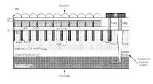
- FIG. 1A is an illustration of an example image sensor 100 A.
- Image sensor 100 A includes plurality of photodiodes 111 disposed in semiconductor material 101 , and through-semiconductor-via (TSV) 103 disposed in semiconductor material 101 .
- TSV 103 is coupled to a negative voltage source.
- Deep trench isolation structures are disposed between individual photodiodes 111 to electrically and optically isolate photodiodes 111 .
- FIG. 1A shows a cross-sectional view of image sensor 100 A, deep trench isolation structures are interconnected in a grid-like pattern to isolate the individual photodiodes 111 .
- the deep trench isolation structures include conductive material 113 (which, as will be shown, are coupled to through-semiconductor-via 103 ), and dielectric material 115 disposed on sidewalls of the deep trench isolation structures (between semiconductor material 101 and conductive material 113 ).
- dielectric material 115 includes hafnium oxide.
- conductive material 113 induces a positive charge in semiconductor material 101 in response to a negative voltage applied from the negative voltage source.
- conductive material 113 includes tungsten.
- image sensor 100 A also includes optical shield 107 disposed on a backside of image sensor 100 A along with metal interconnects 105 .
- a first metal interconnect 105 extends from through-semiconductor-via 103 to optical shield 107
- a second metal interconnect 105 extends from optical shield 107 to conductive material 113 .
- optical shield 107 includes aluminum
- metal interconnects 105 include tungsten and/or copper.
- microlens layer 151 optically aligned with plurality of photodiodes 111 to direct light into plurality of photodiodes 111 .
- Color filter array 131 is disposed between semiconductor material 101 and microlens layer 151 .
- the color filter array 131 may include red, green, and blue color filters which may be arranged into a Bayer pattern, EXR pattern, X-trans pattern, or the like. However, in a different or the same example, the color filter array 131 may include infrared filters, ultraviolet filters, or other light filters that isolate invisible portions of the electromagnetic spectrum. It should be noted that individual color filters 131 are separated by a reflective grid 133 to help direct light to the photodiodes 111 .
- This reflective grid 133 may be vertically aligned with the deep trench isolation structures to promote light absorption in photodiodes 111 .
- reflective grid 133 is connected to optical shield 107 .
- reflective grid 133 and optical shield 107 may include the same material and may be fabricated at the same time.
- Insulation layer 121 is disposed between semiconductor material 101 and color filter array 131 .
- insulation layer 121 also extends across the surface of semiconductor material 101 to the area where TSV 103 connects to optical shield 107 .
- metal interconnects 105 extend through insulation layer 121 to contact optical shield 107 .
- second insulation layer 153 is disposed between the color filter array 131 and microlens layer 151 . Second insulation layer 153 may have the same, or different, material composition as insulation layer 121 .
- Logic wafer 191 (including logic circuitry) is coupled to the semiconductor material 101 .
- the logic circuitry is coupled to plurality of photodiodes 111 to control operation of plurality of photodiodes 111 .
- bonding interface 181 is provided between semiconductor material 101 and logic wafer 191 .
- Through-semiconductor-via 103 extends from semiconductor material 101 into bonding interface 181 and logic wafer 191 .
- TSV 103 may be filled with a metal or other conductive material. The metal may be disposed in the center of TSV 103 while the sides of TSV 103 are lined with oxide or other insulating material to prevent current from flowing into semiconductor material 101 from TSV 103 .
- image sensor 100 A is a backside illuminated image sensor.
- image sensor 100 A may be a frontside illuminated image sensor.
- circuitry e.g., circuitry included in logic wafer 191
- circuitry is located behind the photodiodes so that the circuitry does not block image light.
- circuitry is disposed between the photodiodes and the incident image light.
- FIG. 1B is a magnified view of a deep trench isolation structure from FIG. 1A (see 100 B). Deep trench isolation structures are disposed between individual photodiodes 111 in the plurality of photodiodes 111 . Deep trench isolation structures include dielectric material 115 which is disposed on the sidewalls of the deep trench isolation structures, and conductive material 113 which is disposed in the center of the deep trench isolation structures.
- Deep trench isolation structures are coupled to a through-semiconductor-via (e.g., TSV 103 ), and both the TSV and the deep trench isolation structures are coupled to the optical shield (e.g., optical shield 107 ).
- the through-semiconductor-via is coupled to a negative voltage source, and the negative voltage source induces positive charge accumulation in the semiconductor material 101 proximate to the deep trench isolation structures.
- the negative voltage when the negative voltage is applied to conductive material 113 , positive charge builds up at the interface of semiconductor material 101 and dielectric material 115 .
- Positive charge at the interface of dielectric material 115 and semiconductor material 101 may help to reduce crosstalk between photodiodes 111 because the interface voltage blocks charge transport between surface states in semiconductor material 101 .
- charge from semiconductor material 101 surface states is prevented from moving between pixels on the backside of image sensor 100 A. This mitigates undesirable electrical effects such as dark current and white pixels.
- dielectric material 115 may include hafnium oxide (HfO 2 or HfO x ); however, in other examples, dielectric material 115 may include other oxides such as: silicon oxide (SiO 2 ), silicon nitride (Si 3 N 4 ), silicon oxynitirde (SiO x N y ), tantalum oxide (Ta 2 O 5 ), titanium oxide (TiO 2 ), zirconium oxide (ZrO 2 ), aluminum oxide (Al 2 O 3 ), lanthanum oxide (La 2 O 3 ), praseodymium oxide (Pr 2 O 3 ), cerium oxide (CeO 2 ), neodymium oxide (Nd 2 O 3 ), promethium oxide (Pm 2 O 3 ), samarium oxide (Sm 2 O 3 ), europium oxide (Eu 2 O 3 ), gadolinium oxide (Gd 2 O 3 ), terbium oxide (Tb 2 O 3 ), dysprosium oxide
- dielectric material 115 any stoichiometric combination of the above metals/semiconductors and their oxides/nitrides/oxynitrides may be employed in dielectric material 115 , in accordance with the teachings of the present invention.
- conductive material 113 may include tungsten; however, conductive material 113 may also include metals such as: copper, gold, palladium, silver, aluminum, indium, lead, nickel, titanium, or the like.
- metals such as: copper, gold, palladium, silver, aluminum, indium, lead, nickel, titanium, or the like.
- FIG. 2 illustrates one example of an imaging system 200 including the image sensor of FIG. 1A .
- Imaging system 200 includes pixel array 205 , control circuitry 221 , readout circuitry 211 , and function logic 215 .
- pixel array 205 is a two-dimensional (2D) array of photodiodes, or image sensor pixels (e.g., pixels P 1 , P 2 . . . , Pn).
- photodiodes are arranged into rows (e.g., rows R 1 to Ry) and columns (e.g., column C 1 to Cx) to acquire image data of a person, place, object, etc., which can then be used to render a 2D image of the person, place, object, etc.
- Readout circuitry 211 may be coupled to readout image data from the plurality of photodiodes in pixel array 205 .
- readout circuitry 211 may include amplification circuitry, analog-to-digital (ADC) conversion circuitry, or otherwise.
- Function logic 215 may simply store the image data or even manipulate the image data by applying post image effects (e.g., crop, rotate, remove red eye, adjust brightness, adjust contrast, or otherwise).
- readout circuitry 211 may readout a row of image data at a time along readout column lines (illustrated) or may readout the image data using a variety of other techniques (not illustrated), such as a serial readout or a full parallel readout of all pixels simultaneously.
- control circuitry 221 is coupled to pixel array 205 to control operational of the plurality of photodiodes in pixel array 205 .
- control circuitry 221 may generate a shutter signal for controlling image acquisition.
- the shutter signal is a global shutter signal for simultaneously enabling all pixels within pixel array 205 to simultaneously capture their respective image data during a single acquisition window.
- the shutter signal is a rolling shutter signal such that each row, column, or group of pixels is sequentially enabled during consecutive acquisition windows.
- image acquisition is synchronized with lighting effects such as a flash.
- imaging system 200 may be included in a digital camera, cell phone, laptop computer, or the like. Additionally, imaging system 200 may be coupled to other pieces of hardware such as a processor, memory elements, output (USB port, wireless transmitter, HDMI port, etc.), lighting/flash, electrical input (keyboard, touch display, track pad, mouse, microphone, etc.), and/or display. Other pieces of hardware may deliver instructions to imaging system 200 , extract image data from imaging system 200 , or manipulate image data supplied by imaging system 200 .
- a processor such as a processor, memory elements, output (USB port, wireless transmitter, HDMI port, etc.), lighting/flash, electrical input (keyboard, touch display, track pad, mouse, microphone, etc.), and/or display.
- Other pieces of hardware may deliver instructions to imaging system 200 , extract image data from imaging system 200 , or manipulate image data supplied by imaging system 200 .
- FIG. 3 is a flow chart illustrating a method 300 of image sensor fabrication.
- the order in which some or all blocks appear in method 300 should not be deemed limiting. Rather, one of ordinary skill in the art having the benefit of the present disclosure will understand that some of method 300 may be executed in a variety of orders not illustrated, or even in parallel. Furthermore, method 300 may omit certain blocks in order to avoid obscuring certain aspects. Alternatively, method 300 may include additional blocks that may not be necessary in some embodiments/examples of the disclosure.
- Block 301 illustrates providing the semiconductor material (e.g., semiconductor material 101 ) and the logic wafer (e.g., logic wafer 191 ). In one example these two components are bonded together by a bonding interface (e.g., bonding interface 181 ).
- both the semiconductor material and the logic wafer include silicon; however, in another example, the semiconductor material and the logic wafer may include germanium, arsenic, gallium, or the like. In the example presented here, deep trench isolation structures are already disposed in the semiconductor material.
- Deep trench isolation structures include a dielectric material (e.g., dielectric material 115 ) and a conductive material (e.g., conductive material 113 ), and the dielectric material is disposed between the conductive material and the semiconductor material.
- deep trench isolation structures may have been formed by etching trenches in the semiconductor material and then back-filling the trenches with the dielectric material followed by the conductive material.
- Block 311 describes forming a through-semiconductor-via (TSV) in the semiconductor material.
- TSV through-semiconductor-via
- this involves etching a hole through the semiconductor material to contact interconnects disposed in the bonding interface and logic wafer. Etching of the hole may be achieved by a wet or dry etch depending on the geometry of the via and the desire etch rate. The hole may then be backfilled with an insulating material (like silicon oxide or the like). Another hole is then etched in the insulating material. This new hole is then backfilled with a conductive material (such as a metal or the like). The insulating material prevents electrons from flowing to the semiconductor material from the conductive material.
- Block 321 depicts etching trenches to contact the TSV and the deep trench isolation structures.
- an insulating layer e.g., insulation layer 121 or insulation layer 153
- Holes are then etched into the insulation layer to contact the TSV and the deep trench isolation structures.
- Block 331 illustrates filling the trenches etched in the isolation layer with tungsten.
- tungsten is the choice conductive material, in other examples, many other metals and semiconductors may be used.
- Block 341 describes connecting the tungsten interconnects to the backside optical shield.
- the optical shield is the same material as the metal grid used to separate individual color filters in a color filter array.
- the metal grid is disposed between individual color filters in the color filter array, and helps prevent optical crosstalk between photodiodes.
- Using the optical shield (which is fabricated at the same time as the metal grid, and connected to the metal grid) to connect the through-semiconductor-via to the deep trench isolation structures reduces the number of process steps otherwise required to connect these two pieces of device architecture.
- the metal grid/optical shield may be deposited by thermal evaporation and may include aluminum to enhance its conductivity. However, in other examples, other metals of sufficient conductivity may be used to form the metal grid/optical shield.
- the color filter array may be deposited in the metal grid.
- microlenses may be formed on the color filter array.
- Microlens may be fabricated from a photo-active polymer that is patterned on the surface of the color filter array. Once rectangular blocks of polymer are patterned on the color filter array, the blocks may be melted (or reflowed) to form the dome-like structure characteristic of microlenses.
Landscapes
- Solid State Image Pick-Up Elements (AREA)
Abstract
Description
Claims (10)
Priority Applications (4)
| Application Number | Priority Date | Filing Date | Title |
|---|---|---|---|
| US15/071,035 US9806117B2 (en) | 2016-03-15 | 2016-03-15 | Biased deep trench isolation |
| CN201710068814.2A CN107195644B (en) | 2016-03-15 | 2017-02-08 | Offset deep trench isolation |
| TW106108343A TWI624043B (en) | 2016-03-15 | 2017-03-14 | Bias deep trench isolation |
| US15/717,047 US10269850B2 (en) | 2016-03-15 | 2017-09-27 | Biased deep trench isolation |
Applications Claiming Priority (1)
| Application Number | Priority Date | Filing Date | Title |
|---|---|---|---|
| US15/071,035 US9806117B2 (en) | 2016-03-15 | 2016-03-15 | Biased deep trench isolation |
Related Child Applications (1)
| Application Number | Title | Priority Date | Filing Date |
|---|---|---|---|
| US15/717,047 Division US10269850B2 (en) | 2016-03-15 | 2017-09-27 | Biased deep trench isolation |
Publications (2)
| Publication Number | Publication Date |
|---|---|
| US20170271384A1 US20170271384A1 (en) | 2017-09-21 |
| US9806117B2 true US9806117B2 (en) | 2017-10-31 |
Family
ID=59855896
Family Applications (2)
| Application Number | Title | Priority Date | Filing Date |
|---|---|---|---|
| US15/071,035 Active US9806117B2 (en) | 2016-03-15 | 2016-03-15 | Biased deep trench isolation |
| US15/717,047 Active US10269850B2 (en) | 2016-03-15 | 2017-09-27 | Biased deep trench isolation |
Family Applications After (1)
| Application Number | Title | Priority Date | Filing Date |
|---|---|---|---|
| US15/717,047 Active US10269850B2 (en) | 2016-03-15 | 2017-09-27 | Biased deep trench isolation |
Country Status (3)
| Country | Link |
|---|---|
| US (2) | US9806117B2 (en) |
| CN (1) | CN107195644B (en) |
| TW (1) | TWI624043B (en) |
Cited By (3)
| Publication number | Priority date | Publication date | Assignee | Title |
|---|---|---|---|---|
| US11152415B2 (en) | 2018-10-22 | 2021-10-19 | Samsung Electronics Co., Ltd. | Image sensor with separation pattern and image sensor module including the same |
| US11502120B2 (en) * | 2019-12-19 | 2022-11-15 | Omnivision Technologies, Inc. | Negatively biased isolation structures for pixel devices |
| US11810937B2 (en) | 2020-09-01 | 2023-11-07 | Samsung Electronics Co., Ltd. | Image sensor and method for fabricating the same |
Families Citing this family (18)
| Publication number | Priority date | Publication date | Assignee | Title |
|---|---|---|---|---|
| JP7007088B2 (en) * | 2016-12-07 | 2022-01-24 | ソニーセミコンダクタソリューションズ株式会社 | Light receiving elements, image sensors and electronic devices |
| EP3422424B1 (en) * | 2017-06-27 | 2022-09-07 | ams AG | Semiconductor photodetector device with protection against ambient back light |
| CN107910297A (en) * | 2017-12-07 | 2018-04-13 | 德淮半导体有限公司 | The manufacture method and back side illumination image sensor of back side illumination image sensor |
| US10325889B1 (en) * | 2018-01-12 | 2019-06-18 | Mikro Mesa Technology Co., Ltd. | Display device including LED devices with selective activation function |
| CN108281448A (en) * | 2018-01-30 | 2018-07-13 | 德淮半导体有限公司 | The manufacturing method of back side illumination image sensor |
| CN108538874B (en) * | 2018-05-07 | 2021-03-02 | 德淮半导体有限公司 | Image sensor and method of forming the same |
| CN108600660B (en) * | 2018-05-16 | 2020-06-30 | 上海集成电路研发中心有限公司 | Dark current real-time calibration image sensor and calibration method |
| KR102636443B1 (en) * | 2018-12-12 | 2024-02-15 | 에스케이하이닉스 주식회사 | Image sensing device including noise blocking structure |
| CN110085614A (en) * | 2019-04-30 | 2019-08-02 | 德淮半导体有限公司 | Back side illumination image sensor and its manufacturing method |
| US11538836B2 (en) * | 2020-08-13 | 2022-12-27 | Omnivision Technologies, Inc. | Cell deep trench isolation pyramid structures for CMOS image sensors |
| US11570339B2 (en) * | 2020-09-30 | 2023-01-31 | Lextar Electronics Corporation | Photodiode package structure with shutters, forming method thereof, and wearable device having the same |
| US11908878B2 (en) * | 2021-01-15 | 2024-02-20 | Taiwan Semiconductor Manufacturing Company, Ltd. | Image sensor and manufacturing method thereof |
| US12176370B2 (en) | 2021-01-27 | 2024-12-24 | Taiwan Semiconductor Manufacturing Company, Ltd. | Stacked structure for CMOS image sensors including through-substrate-via contacting negative bias circuit |
| KR20220108609A (en) * | 2021-01-27 | 2022-08-03 | 삼성전자주식회사 | Image sensor, pixel and operatin g method of image sensor |
| CN113948538B (en) * | 2021-09-18 | 2025-07-29 | 上海华力集成电路制造有限公司 | Backside illuminated image sensor and method of manufacturing the same |
| US12464837B2 (en) | 2022-02-03 | 2025-11-04 | Omnivision Technologies, Inc. | High dynamic range, backside-illuminated, low crosstalk image sensor with walls on backside surface to isolate photodiodes |
| JP2023169473A (en) * | 2022-05-17 | 2023-11-30 | シャープディスプレイテクノロジー株式会社 | Active matrix substrate, liquid crystal display device, and method for manufacturing active matrix substrate |
| CN119133199A (en) * | 2024-11-12 | 2024-12-13 | 荣芯半导体(宁波)有限公司 | Image sensor and method for manufacturing the same |
Citations (2)
| Publication number | Priority date | Publication date | Assignee | Title |
|---|---|---|---|---|
| US20140016012A1 (en) * | 2012-07-13 | 2014-01-16 | Kabushiki Kaisha Toshiba | Solid state imaging device |
| US20140291481A1 (en) | 2013-04-01 | 2014-10-02 | Omnivision Technologies, Inc. | Enhanced photon detection device with biased deep trench isolation |
Family Cites Families (13)
| Publication number | Priority date | Publication date | Assignee | Title |
|---|---|---|---|---|
| KR20130106978A (en) * | 2012-03-21 | 2013-10-01 | 삼성전자주식회사 | Unit pixel of image sensor and image sensor including the same |
| US8686342B2 (en) * | 2012-04-09 | 2014-04-01 | Omnivision Technologies, Inc. | Double-sided image sensor formed on a single semiconductor wafer die |
| KR101934864B1 (en) * | 2012-05-30 | 2019-03-18 | 삼성전자주식회사 | Through silicon via structure, methods of forming the same, image sensor including the through silicon via structure and methods of manufacturing the image sensor |
| US8878325B2 (en) * | 2012-07-31 | 2014-11-04 | Taiwan Semiconductor Manufacturing Company, Ltd. | Elevated photodiode with a stacked scheme |
| US8933527B2 (en) * | 2012-07-31 | 2015-01-13 | Taiwan Semiconductor Manufacturing Company, Ltd. | Elevated photodiodes with crosstalk isolation |
| KR102034482B1 (en) * | 2013-03-04 | 2019-10-21 | 삼성전자주식회사 | Image sensor and method of forming the same |
| KR20140147508A (en) * | 2013-06-20 | 2014-12-30 | 삼성전자주식회사 | Image sensor |
| US9496304B2 (en) * | 2013-08-15 | 2016-11-15 | Omnivision Technologies, Inc. | Image sensor pixel cell with switched deep trench isolation structure |
| JP6465545B2 (en) * | 2013-09-27 | 2019-02-06 | ソニー株式会社 | Imaging device, manufacturing method thereof, and electronic apparatus |
| KR102180102B1 (en) * | 2014-03-07 | 2020-11-17 | 삼성전자주식회사 | Image Sensor and Method of Fabricating the Same |
| US9111993B1 (en) * | 2014-08-21 | 2015-08-18 | Omnivision Technologies, Inc. | Conductive trench isolation |
| KR102374110B1 (en) * | 2014-08-22 | 2022-03-14 | 삼성전자주식회사 | Image Sensors Having a Shielding Structure |
| US9515111B2 (en) * | 2014-10-20 | 2016-12-06 | Semiconductor Components Industries, Llc | Circuitry for biasing light shielding structures and deep trench isolation structures |
-
2016
- 2016-03-15 US US15/071,035 patent/US9806117B2/en active Active
-
2017
- 2017-02-08 CN CN201710068814.2A patent/CN107195644B/en active Active
- 2017-03-14 TW TW106108343A patent/TWI624043B/en active
- 2017-09-27 US US15/717,047 patent/US10269850B2/en active Active
Patent Citations (2)
| Publication number | Priority date | Publication date | Assignee | Title |
|---|---|---|---|---|
| US20140016012A1 (en) * | 2012-07-13 | 2014-01-16 | Kabushiki Kaisha Toshiba | Solid state imaging device |
| US20140291481A1 (en) | 2013-04-01 | 2014-10-02 | Omnivision Technologies, Inc. | Enhanced photon detection device with biased deep trench isolation |
Cited By (3)
| Publication number | Priority date | Publication date | Assignee | Title |
|---|---|---|---|---|
| US11152415B2 (en) | 2018-10-22 | 2021-10-19 | Samsung Electronics Co., Ltd. | Image sensor with separation pattern and image sensor module including the same |
| US11502120B2 (en) * | 2019-12-19 | 2022-11-15 | Omnivision Technologies, Inc. | Negatively biased isolation structures for pixel devices |
| US11810937B2 (en) | 2020-09-01 | 2023-11-07 | Samsung Electronics Co., Ltd. | Image sensor and method for fabricating the same |
Also Published As
| Publication number | Publication date |
|---|---|
| CN107195644A (en) | 2017-09-22 |
| CN107195644B (en) | 2021-05-18 |
| US20180033811A1 (en) | 2018-02-01 |
| TWI624043B (en) | 2018-05-11 |
| US20170271384A1 (en) | 2017-09-21 |
| US10269850B2 (en) | 2019-04-23 |
| TW201735336A (en) | 2017-10-01 |
Similar Documents
| Publication | Publication Date | Title |
|---|---|---|
| US10269850B2 (en) | Biased deep trench isolation | |
| US11056524B2 (en) | Image pickup device, method of manufacturing image pickup device, and electronic apparatus | |
| US9240431B1 (en) | Conductive trench isolation | |
| US9659989B1 (en) | Image sensor with semiconductor trench isolation | |
| TWI649866B (en) | Image sensor with hybrid deep trench isolation | |
| US8450728B2 (en) | Solid-state imaging device, method of manufacturing the same, and electronic apparatus | |
| US10224364B2 (en) | CMOS image sensor having enhanced near infrared quantum efficiency and modulation transfer function | |
| CN109216385B (en) | CMOS image sensor with enhanced near-infrared quantum efficiency | |
| CN110993630B (en) | Multiple Thickness Gate Dielectrics | |
| US20210193723A1 (en) | Tunnel contact for a pixel cell in an imaging system | |
| US9986192B1 (en) | Through-semiconductor and through-dielectric isolation structure | |
| US10438979B2 (en) | Method of fabricating fill factor enhancement for image sensor | |
| US9799696B1 (en) | Isolation structure in photodiode | |
| US9564470B1 (en) | Hard mask as contact etch stop layer in image sensors | |
| US20170162621A1 (en) | Light channels with multi-step etch | |
| HK1216802B (en) | Image sensor and methods for image sensor fabrication |
Legal Events
| Date | Code | Title | Description |
|---|---|---|---|
| AS | Assignment |
Owner name: OMNIVISION TECHNOLOGIES, INC., CALIFORNIA Free format text: ASSIGNMENT OF ASSIGNORS INTEREST;ASSIGNORS:ZHENG, YUANWEI;CHEN, GANG;MAO, DULI;AND OTHERS;SIGNING DATES FROM 20160307 TO 20160312;REEL/FRAME:037990/0918 |
|
| STCF | Information on status: patent grant |
Free format text: PATENTED CASE |
|
| MAFP | Maintenance fee payment |
Free format text: PAYMENT OF MAINTENANCE FEE, 4TH YEAR, LARGE ENTITY (ORIGINAL EVENT CODE: M1551); ENTITY STATUS OF PATENT OWNER: LARGE ENTITY Year of fee payment: 4 |
|
| MAFP | Maintenance fee payment |
Free format text: PAYMENT OF MAINTENANCE FEE, 8TH YEAR, LARGE ENTITY (ORIGINAL EVENT CODE: M1552); ENTITY STATUS OF PATENT OWNER: LARGE ENTITY Year of fee payment: 8 |