US9804464B2 - Array substrate and method for preparing the same, liquid crystal panel - Google Patents

Array substrate and method for preparing the same, liquid crystal panel Download PDF

Info

Publication number
US9804464B2
US9804464B2 US14/777,876 US201514777876A US9804464B2 US 9804464 B2 US9804464 B2 US 9804464B2 US 201514777876 A US201514777876 A US 201514777876A US 9804464 B2 US9804464 B2 US 9804464B2
Authority
US
United States
Prior art keywords
thin film
source
region
electrode
glass substrate
Prior art date
Legal status (The legal status is an assumption and is not a legal conclusion. Google has not performed a legal analysis and makes no representation as to the accuracy of the status listed.)
Expired - Fee Related, expires
Application number
US14/777,876
Other versions
US20170108722A1 (en
Inventor
Dongzi Gao
Current Assignee (The listed assignees may be inaccurate. Google has not performed a legal analysis and makes no representation or warranty as to the accuracy of the list.)
TCL China Star Optoelectronics Technology Co Ltd
Original Assignee
Shenzhen China Star Optoelectronics Technology Co Ltd
Priority date (The priority date is an assumption and is not a legal conclusion. Google has not performed a legal analysis and makes no representation as to the accuracy of the date listed.)
Filing date
Publication date
Application filed by Shenzhen China Star Optoelectronics Technology Co Ltd filed Critical Shenzhen China Star Optoelectronics Technology Co Ltd
Assigned to SHENZHEN CHINA STAR OPTOELECTRONICS TECHNOLOGY CO., LTD. reassignment SHENZHEN CHINA STAR OPTOELECTRONICS TECHNOLOGY CO., LTD. ASSIGNMENT OF ASSIGNORS INTEREST (SEE DOCUMENT FOR DETAILS). Assignors: GAO, DONGZI
Publication of US20170108722A1 publication Critical patent/US20170108722A1/en
Application granted granted Critical
Publication of US9804464B2 publication Critical patent/US9804464B2/en
Expired - Fee Related legal-status Critical Current
Adjusted expiration legal-status Critical

Links

Images

Classifications

    • GPHYSICS
    • G02OPTICS
    • G02FOPTICAL DEVICES OR ARRANGEMENTS FOR THE CONTROL OF LIGHT BY MODIFICATION OF THE OPTICAL PROPERTIES OF THE MEDIA OF THE ELEMENTS INVOLVED THEREIN; NON-LINEAR OPTICS; FREQUENCY-CHANGING OF LIGHT; OPTICAL LOGIC ELEMENTS; OPTICAL ANALOGUE/DIGITAL CONVERTERS
    • G02F1/00Devices or arrangements for the control of the intensity, colour, phase, polarisation or direction of light arriving from an independent light source, e.g. switching, gating or modulating; Non-linear optics
    • G02F1/01Devices or arrangements for the control of the intensity, colour, phase, polarisation or direction of light arriving from an independent light source, e.g. switching, gating or modulating; Non-linear optics for the control of the intensity, phase, polarisation or colour 
    • G02F1/13Devices or arrangements for the control of the intensity, colour, phase, polarisation or direction of light arriving from an independent light source, e.g. switching, gating or modulating; Non-linear optics for the control of the intensity, phase, polarisation or colour  based on liquid crystals, e.g. single liquid crystal display cells
    • G02F1/133Constructional arrangements; Operation of liquid crystal cells; Circuit arrangements
    • G02F1/136Liquid crystal cells structurally associated with a semi-conducting layer or substrate, e.g. cells forming part of an integrated circuit
    • G02F1/1362Active matrix addressed cells
    • G02F1/1368Active matrix addressed cells in which the switching element is a three-electrode device
    • GPHYSICS
    • G02OPTICS
    • G02FOPTICAL DEVICES OR ARRANGEMENTS FOR THE CONTROL OF LIGHT BY MODIFICATION OF THE OPTICAL PROPERTIES OF THE MEDIA OF THE ELEMENTS INVOLVED THEREIN; NON-LINEAR OPTICS; FREQUENCY-CHANGING OF LIGHT; OPTICAL LOGIC ELEMENTS; OPTICAL ANALOGUE/DIGITAL CONVERTERS
    • G02F1/00Devices or arrangements for the control of the intensity, colour, phase, polarisation or direction of light arriving from an independent light source, e.g. switching, gating or modulating; Non-linear optics
    • G02F1/01Devices or arrangements for the control of the intensity, colour, phase, polarisation or direction of light arriving from an independent light source, e.g. switching, gating or modulating; Non-linear optics for the control of the intensity, phase, polarisation or colour 
    • G02F1/13Devices or arrangements for the control of the intensity, colour, phase, polarisation or direction of light arriving from an independent light source, e.g. switching, gating or modulating; Non-linear optics for the control of the intensity, phase, polarisation or colour  based on liquid crystals, e.g. single liquid crystal display cells
    • G02F1/133Constructional arrangements; Operation of liquid crystal cells; Circuit arrangements
    • G02F1/1333Constructional arrangements; Manufacturing methods
    • G02F1/133345Insulating layers
    • GPHYSICS
    • G02OPTICS
    • G02FOPTICAL DEVICES OR ARRANGEMENTS FOR THE CONTROL OF LIGHT BY MODIFICATION OF THE OPTICAL PROPERTIES OF THE MEDIA OF THE ELEMENTS INVOLVED THEREIN; NON-LINEAR OPTICS; FREQUENCY-CHANGING OF LIGHT; OPTICAL LOGIC ELEMENTS; OPTICAL ANALOGUE/DIGITAL CONVERTERS
    • G02F1/00Devices or arrangements for the control of the intensity, colour, phase, polarisation or direction of light arriving from an independent light source, e.g. switching, gating or modulating; Non-linear optics
    • G02F1/01Devices or arrangements for the control of the intensity, colour, phase, polarisation or direction of light arriving from an independent light source, e.g. switching, gating or modulating; Non-linear optics for the control of the intensity, phase, polarisation or colour 
    • G02F1/13Devices or arrangements for the control of the intensity, colour, phase, polarisation or direction of light arriving from an independent light source, e.g. switching, gating or modulating; Non-linear optics for the control of the intensity, phase, polarisation or colour  based on liquid crystals, e.g. single liquid crystal display cells
    • G02F1/133Constructional arrangements; Operation of liquid crystal cells; Circuit arrangements
    • G02F1/1333Constructional arrangements; Manufacturing methods
    • G02F1/1335Structural association of cells with optical devices, e.g. polarisers or reflectors
    • G02F1/133509Filters, e.g. light shielding masks
    • G02F1/133514Colour filters
    • GPHYSICS
    • G02OPTICS
    • G02FOPTICAL DEVICES OR ARRANGEMENTS FOR THE CONTROL OF LIGHT BY MODIFICATION OF THE OPTICAL PROPERTIES OF THE MEDIA OF THE ELEMENTS INVOLVED THEREIN; NON-LINEAR OPTICS; FREQUENCY-CHANGING OF LIGHT; OPTICAL LOGIC ELEMENTS; OPTICAL ANALOGUE/DIGITAL CONVERTERS
    • G02F1/00Devices or arrangements for the control of the intensity, colour, phase, polarisation or direction of light arriving from an independent light source, e.g. switching, gating or modulating; Non-linear optics
    • G02F1/01Devices or arrangements for the control of the intensity, colour, phase, polarisation or direction of light arriving from an independent light source, e.g. switching, gating or modulating; Non-linear optics for the control of the intensity, phase, polarisation or colour 
    • G02F1/13Devices or arrangements for the control of the intensity, colour, phase, polarisation or direction of light arriving from an independent light source, e.g. switching, gating or modulating; Non-linear optics for the control of the intensity, phase, polarisation or colour  based on liquid crystals, e.g. single liquid crystal display cells
    • G02F1/133Constructional arrangements; Operation of liquid crystal cells; Circuit arrangements
    • G02F1/1333Constructional arrangements; Manufacturing methods
    • G02F1/1343Electrodes
    • G02F1/134309Electrodes characterised by their geometrical arrangement
    • GPHYSICS
    • G02OPTICS
    • G02FOPTICAL DEVICES OR ARRANGEMENTS FOR THE CONTROL OF LIGHT BY MODIFICATION OF THE OPTICAL PROPERTIES OF THE MEDIA OF THE ELEMENTS INVOLVED THEREIN; NON-LINEAR OPTICS; FREQUENCY-CHANGING OF LIGHT; OPTICAL LOGIC ELEMENTS; OPTICAL ANALOGUE/DIGITAL CONVERTERS
    • G02F1/00Devices or arrangements for the control of the intensity, colour, phase, polarisation or direction of light arriving from an independent light source, e.g. switching, gating or modulating; Non-linear optics
    • G02F1/01Devices or arrangements for the control of the intensity, colour, phase, polarisation or direction of light arriving from an independent light source, e.g. switching, gating or modulating; Non-linear optics for the control of the intensity, phase, polarisation or colour 
    • G02F1/13Devices or arrangements for the control of the intensity, colour, phase, polarisation or direction of light arriving from an independent light source, e.g. switching, gating or modulating; Non-linear optics for the control of the intensity, phase, polarisation or colour  based on liquid crystals, e.g. single liquid crystal display cells
    • G02F1/133Constructional arrangements; Operation of liquid crystal cells; Circuit arrangements
    • G02F1/136Liquid crystal cells structurally associated with a semi-conducting layer or substrate, e.g. cells forming part of an integrated circuit
    • G02F1/1362Active matrix addressed cells
    • G02F1/136227Through-hole connection of the pixel electrode to the active element through an insulation layer
    • GPHYSICS
    • G02OPTICS
    • G02FOPTICAL DEVICES OR ARRANGEMENTS FOR THE CONTROL OF LIGHT BY MODIFICATION OF THE OPTICAL PROPERTIES OF THE MEDIA OF THE ELEMENTS INVOLVED THEREIN; NON-LINEAR OPTICS; FREQUENCY-CHANGING OF LIGHT; OPTICAL LOGIC ELEMENTS; OPTICAL ANALOGUE/DIGITAL CONVERTERS
    • G02F1/00Devices or arrangements for the control of the intensity, colour, phase, polarisation or direction of light arriving from an independent light source, e.g. switching, gating or modulating; Non-linear optics
    • G02F1/01Devices or arrangements for the control of the intensity, colour, phase, polarisation or direction of light arriving from an independent light source, e.g. switching, gating or modulating; Non-linear optics for the control of the intensity, phase, polarisation or colour 
    • G02F1/13Devices or arrangements for the control of the intensity, colour, phase, polarisation or direction of light arriving from an independent light source, e.g. switching, gating or modulating; Non-linear optics for the control of the intensity, phase, polarisation or colour  based on liquid crystals, e.g. single liquid crystal display cells
    • G02F1/133Constructional arrangements; Operation of liquid crystal cells; Circuit arrangements
    • G02F1/136Liquid crystal cells structurally associated with a semi-conducting layer or substrate, e.g. cells forming part of an integrated circuit
    • G02F1/1362Active matrix addressed cells
    • G02F1/136286Wiring, e.g. gate line, drain line
    • GPHYSICS
    • G02OPTICS
    • G02FOPTICAL DEVICES OR ARRANGEMENTS FOR THE CONTROL OF LIGHT BY MODIFICATION OF THE OPTICAL PROPERTIES OF THE MEDIA OF THE ELEMENTS INVOLVED THEREIN; NON-LINEAR OPTICS; FREQUENCY-CHANGING OF LIGHT; OPTICAL LOGIC ELEMENTS; OPTICAL ANALOGUE/DIGITAL CONVERTERS
    • G02F1/00Devices or arrangements for the control of the intensity, colour, phase, polarisation or direction of light arriving from an independent light source, e.g. switching, gating or modulating; Non-linear optics
    • G02F1/01Devices or arrangements for the control of the intensity, colour, phase, polarisation or direction of light arriving from an independent light source, e.g. switching, gating or modulating; Non-linear optics for the control of the intensity, phase, polarisation or colour 
    • G02F1/13Devices or arrangements for the control of the intensity, colour, phase, polarisation or direction of light arriving from an independent light source, e.g. switching, gating or modulating; Non-linear optics for the control of the intensity, phase, polarisation or colour  based on liquid crystals, e.g. single liquid crystal display cells
    • G02F1/133Constructional arrangements; Operation of liquid crystal cells; Circuit arrangements
    • G02F1/1333Constructional arrangements; Manufacturing methods
    • G02F1/133302Rigid substrates, e.g. inorganic substrates
    • GPHYSICS
    • G02OPTICS
    • G02FOPTICAL DEVICES OR ARRANGEMENTS FOR THE CONTROL OF LIGHT BY MODIFICATION OF THE OPTICAL PROPERTIES OF THE MEDIA OF THE ELEMENTS INVOLVED THEREIN; NON-LINEAR OPTICS; FREQUENCY-CHANGING OF LIGHT; OPTICAL LOGIC ELEMENTS; OPTICAL ANALOGUE/DIGITAL CONVERTERS
    • G02F1/00Devices or arrangements for the control of the intensity, colour, phase, polarisation or direction of light arriving from an independent light source, e.g. switching, gating or modulating; Non-linear optics
    • G02F1/01Devices or arrangements for the control of the intensity, colour, phase, polarisation or direction of light arriving from an independent light source, e.g. switching, gating or modulating; Non-linear optics for the control of the intensity, phase, polarisation or colour 
    • G02F1/13Devices or arrangements for the control of the intensity, colour, phase, polarisation or direction of light arriving from an independent light source, e.g. switching, gating or modulating; Non-linear optics for the control of the intensity, phase, polarisation or colour  based on liquid crystals, e.g. single liquid crystal display cells
    • G02F1/133Constructional arrangements; Operation of liquid crystal cells; Circuit arrangements
    • G02F1/136Liquid crystal cells structurally associated with a semi-conducting layer or substrate, e.g. cells forming part of an integrated circuit
    • G02F1/1362Active matrix addressed cells
    • G02F1/136286Wiring, e.g. gate line, drain line
    • G02F1/136295Materials; Compositions; Manufacture processes
    • G02F2001/133302
    • G02F2001/136295
    • GPHYSICS
    • G02OPTICS
    • G02FOPTICAL DEVICES OR ARRANGEMENTS FOR THE CONTROL OF LIGHT BY MODIFICATION OF THE OPTICAL PROPERTIES OF THE MEDIA OF THE ELEMENTS INVOLVED THEREIN; NON-LINEAR OPTICS; FREQUENCY-CHANGING OF LIGHT; OPTICAL LOGIC ELEMENTS; OPTICAL ANALOGUE/DIGITAL CONVERTERS
    • G02F2201/00Constructional arrangements not provided for in groups G02F1/00 - G02F7/00
    • G02F2201/12Constructional arrangements not provided for in groups G02F1/00 - G02F7/00 electrode
    • G02F2201/123Constructional arrangements not provided for in groups G02F1/00 - G02F7/00 electrode pixel
    • HELECTRICITY
    • H10SEMICONDUCTOR DEVICES; ELECTRIC SOLID-STATE DEVICES NOT OTHERWISE PROVIDED FOR
    • H10DINORGANIC ELECTRIC SEMICONDUCTOR DEVICES
    • H10D86/00Integrated devices formed in or on insulating or conducting substrates, e.g. formed in silicon-on-insulator [SOI] substrates or on stainless steel or glass substrates
    • H10D86/40Integrated devices formed in or on insulating or conducting substrates, e.g. formed in silicon-on-insulator [SOI] substrates or on stainless steel or glass substrates characterised by multiple TFTs
    • H10D86/441Interconnections, e.g. scanning lines
    • HELECTRICITY
    • H10SEMICONDUCTOR DEVICES; ELECTRIC SOLID-STATE DEVICES NOT OTHERWISE PROVIDED FOR
    • H10DINORGANIC ELECTRIC SEMICONDUCTOR DEVICES
    • H10D86/00Integrated devices formed in or on insulating or conducting substrates, e.g. formed in silicon-on-insulator [SOI] substrates or on stainless steel or glass substrates
    • H10D86/40Integrated devices formed in or on insulating or conducting substrates, e.g. formed in silicon-on-insulator [SOI] substrates or on stainless steel or glass substrates characterised by multiple TFTs
    • H10D86/60Integrated devices formed in or on insulating or conducting substrates, e.g. formed in silicon-on-insulator [SOI] substrates or on stainless steel or glass substrates characterised by multiple TFTs wherein the TFTs are in active matrices

Definitions

  • the present invention relates to liquid crystal display technical field, and more particularly, to an array substrate and a method of preparing the same, as well as a liquid crystal panel including the array substrate.
  • a liquid crystal display is a display apparatus of which the panel is ultra-thin, and a liquid crystal panel is an importance component of the LCD.
  • Common liquid crystal panel at least comprises an array substrate and a color filter substrate disposed opposite to each other, and a liquid crystal layer between the array substrate and the color filter substrate.
  • FIG. 1 is a block diagram of an existing array substrate and merely shows an exemplary pixel structure therein.
  • a pixel structure 1 includes a light transmitting region 1 a and a light non-transmitting region 1 b
  • the light non-transmitting region 1 b includes a gate electrode 3 , a gate insulating layer 4 , an active layer 5 , an ohmic contact layer 6 , source/drain electrodes 7 a and 7 b , and a passivation layer 8 sequentially formed on a glass substrate 2
  • the light transmitting region 1 a includes a gate insulating layer 4 , a passivation layer 8 and a pixel electrode 9 sequentially formed on the glass substrate 2
  • the pixel electrode 9 extends to the light non-transmitting region 1 b and is electrically connected to the source electrode 7 a or drain electrode 7 b through a via
  • the light emitted from the backlight is absorbed and refracted through a polarizer, a glass substrate, a liquid crystal layer and a color filter etc successively, and then the light transmittance is about 6%, thus increasing light transmittance is effective to improve utilization of backlight.
  • the array substrate with the above structure as shown in FIG. 1 , in the light transmitting region 1 a of the pixel structure 1 , between the pixel electrode 9 and the glass substrate 2 also includes the gate insulating layer 4 and the passivation layer 8 .
  • the gate insulating layer 4 and the passivation layer 8 mainly server to separate different metal layers in the light non-transmitting region 1 b , but with respect to the pixel electrode 9 and the glass substrate 2 in the light transmitting region 1 a , the gate insulating layer 4 and the passivation layer 8 are redundant and may absorb and refract a part of light so as to loss part of light, such that the light transmittance is decreased, to thereby reduce the utilization of the backlight.
  • the present invention provides an array substrate and the method of preparing the same, and by improving the pixel structure in the array substrate, the light transmittance of the light transmitting region in the pixel structure is increased, thus the utilization of the backlight is increased.
  • the present invention adopts the following technical solution:
  • An array substrate includes a glass substrate and a plurality of pixel structures formed on the glass substrate, each pixel structure includes a light transmitting region and a light non-transmitting region, wherein the light non-transmitting region includes a gate electrode, a gate insulating layer, an active layer, a source electrode, a drain electrode and a passivation layer which are sequentially formed on the glass substrate; the light transmitting region includes a pixel electrode which is directly formed on the glass substrate, and the pixel electrode extends to the light non-transmitting region and is electrically connected to the source electrode or the drain electrode.
  • a via hole is provided on the passivation layer and through which the pixel electrode is electrically connected to the source electrode or the drain electrode.
  • an ohmic contact layer is provided between the active layer and the source/drain electrodes.
  • the material of the gate insulating layer is SiN x or SiO x .
  • the material of the passivation layer is SiN x or SiO x .
  • a method of preparing a array substrate comprises the following steps:
  • step S 30 preparing a passivation layer thin film on the glass substrate after step S 20 , wherein the passivation layer thin film covers the light transmitting region and the light non-transmitting region of the pixel structure;
  • step S 50 preparing a pixel electrode on the glass substrate after step S 40 , wherein the pixel electrode in the light transmitting region is connected to glass substrate, and the pixel electrode is electrically connected to the source electrode or the drain electrode through the via hole.
  • Step S 10 specifically includes:
  • Step S 20 specifically includes:
  • Step S 40 specifically includes:
  • photoresist on the passivation layer thin film, and exposing the passivation layer thin film on a via hole region and the light transmitting region by exposing and developing the photoresist;
  • An embodiment of the present invention also provides a liquid crystal panel which includes an array substrate and a color filter substrate disposed opposite to each other, and a liquid crystal layer between the array substrate and the color filter substrate, wherein the array substrate uses the above mentioned array substrate.
  • the array substrate and the liquid crystal panel provided according to the embodiments of the present invention improve the pixel structure in the array substrate by removing the gate insulating layer and the passivation layer in the light transmitting region, such that the pixel electrode in the light transmitting region is directly disposed on the glass substrate, to thereby increase the light transmittance of the light transmitting region in the pixel structure, and increase the utilization of the backlight.
  • FIG. 1 is a structural diagram of an existing array substrate.
  • FIG. 2 is a structure diagram of the array substrate provided by an embodiment of the present invention.
  • FIGS. 3 a -3 h illustrate steps for forming products in the preparation method provided by an embodiment of the present invention.
  • FIG. 4 is a structure diagram of the liquid crystal panel provided in the embodiment of the present invention.
  • the embodiment provides an array substrate which includes a glass substrate 20 and a plurality of pixel structures 10 ( FIG. 2 shows exemplary part sectioned view of a pixel structure 10 therein) formed on the glass substrate 20 , wherein the pixel structure 10 includes a light transmitting region 10 a and a light non-transmitting region 10 b .
  • the light non-transmitting region 10 b includes a gate electrode 30 , a gate insulating layer 40 , an active layer 50 , a source electrode 70 a , a drain electrode 70 b , and a passivation layer 80 sequentially formed on the glass substrate 20 .
  • the light transmitting region 10 a includes a pixel electrode 90 which is directly formed on the glass substrate 20 , and the pixel electrode 90 extends to the light non-transmitting region 10 b and is electrically connected to the source/drain electrodes 70 a and 70 b (here should be understood that the pixel electrode 90 is electrically connected to one of the source electrode 70 a and the drain electrode 70 b ). Furthermore, to allow the source/drain electrodes 70 a and 70 b to be well electrically connected to the active layer 50 , an ohmic contact layer 60 is provided between the active layer 50 and the source/drain electrodes 70 a and 70 b.
  • the passivation layer 80 is provided with a via hole 80 a thereon through which the pixel electrode 90 is electrically connected to the source electrode 70 a or the drain electrode 70 b.
  • the material of the gate insulating layer 40 can be SiN x or SiO x
  • the material of the passivation layer 80 can be SiN x or SiO x .
  • the gate insulating layer and the passivation layer are removed from the light transmitting region, such that the pixel electrode in the light transmitting region is directly disposed on the glass substrate, thus the light transmittance of the light transmitting region in the pixel structure is increase, so as to increase the utilization of the backlight.
  • the method of preparing the array substrate comprises the following steps:
  • S 10 preparing a gate electrode 30 on the glass substrate 20 .
  • a layer of gate metal thin film 30 a is formed on the glass substrate 20 ; and then the gate metal thin film 30 a is coated with photoresist, and the photoresist of the gate pattern region is reserved by exposing and developing the photoresist; and finally, the exposed gate metal thin film 30 a is etched away and the residual photoresist is removed to form the gate electrode 30 .
  • step S 20 sequentially preparing the gate insulating layer thin film 40 a , the active layer 50 , the ohmic contact layer 60 , and the source/drain electrodes 70 a and 70 b on the glass substrate 20 after step S 10 , wherein the gate insulating layer thin film 40 a covers the light transmitting region 10 a and the light non-transmitting region 10 b of the pixel structure 10 .
  • the gate insulating layer thin film 40 a , the active layer thin film 50 a , the ohmic contact layer thin film 60 a , and the source/drain metal thin film 70 are sequentially formed on the glass substrate 20 on which the gate electrode 30 is formed, wherein the source/drain metal thin film 70 is coated with photoresist (not show in the figure), as shown in FIG. 3 c.
  • the photoresist is exposed and developed with a double-tone mask, and the photoresist corresponding to a source region 70 a and a drain region 70 b , and the photoresist corresponding to a channel region are retained; and the exposed source/drain metal thin film 70 , the ohmic contact layer thin film 60 a and the active layer thin film 50 a are etched away to obtain the structure shown in FIG. 3 d.
  • the photoresist corresponding to the channel region is removed through ashing process, the ohmic contact layer thin film 60 a and the source/drain metal thin film 70 above the channel region are etched, and the residual photoresist is removed to get the gate insulating thin film 40 a , the active layer 50 , the ohmic contact layer 60 and the source/drain electrodes 70 a and 70 b , as shown in FIG. 3 e.
  • step S 30 preparing a passivation layer thin film 80 b on the glass substrate 20 after step S 20 , wherein the passivation layer thin film 80 b covers the light transmitting region 10 a and the light non-transmitting region 10 b of the pixel structure 10 , as shown in FIG. 3 f .
  • the passivation thin film 80 b is coated with photoresist, and the passivation thin film 80 b is exposed on a via hole region 80 a and the light transmitting region 10 a by exposing and developing the photoresist; the passivation layer thin film 80 b is removed from the via hole region 80 a through etching process to obtain the via hole 80 a ; and then the light transmitting region 10 a exposes the glass substrate 20 by etching away the passivation layer thin film 80 b and the gate insulating layer thin film 40 a , as shown in FIG. 3 g .
  • step S 50 preparing the pixel electrode 90 on the glass substrate 20 after step S 40 , wherein the pixel electrode 90 in the light transmitting region 10 a is directly connected to glass substrate 20 , and the pixel electrode 90 is electrically connected to the source electrode 70 a or drain electrode 70 b through the via hole 80 a , as shown in FIG. 3 h.
  • step S 40 through one-mask process in step S 40 , the gate insulating layer thin film and the passivation layer thin film covered on the light transmitting region are etched away when preparing the via hole, no extra process is required, and the process is simple and easy-implementation, and in the end, an array substrate having higher transmittance is prepared.
  • An embodiment of the present invention also provides a liquid crystal panel, as shown in FIG. 4 , the liquid crystal panel includes an array substrate 100 and a color filter substrate 200 disposed opposite to each other, and a liquid crystal layer 300 between the array substrate 100 and the color filter substrate 200 , wherein the array substrate 100 uses the array substrate provided in the embodiment.
  • the array substrate and the liquid crystal panel provided according to the embodiments of the present invention improve the pixel structure in the array substrate by removing the gate insulating layer and the passivation layer in the light transmitting region, such that the pixel electrode in the light transmitting region is directly disposed on the glass substrate, to thereby increase the light transmittance of the light transmitting region in the pixel structure, and increase the utilization of the backlight.

Landscapes

  • Physics & Mathematics (AREA)
  • Nonlinear Science (AREA)
  • Mathematical Physics (AREA)
  • Chemical & Material Sciences (AREA)
  • Crystallography & Structural Chemistry (AREA)
  • General Physics & Mathematics (AREA)
  • Optics & Photonics (AREA)
  • Engineering & Computer Science (AREA)
  • Microelectronics & Electronic Packaging (AREA)
  • Geometry (AREA)
  • Thin Film Transistor (AREA)
  • Liquid Crystal (AREA)

Abstract

An array substrate includes a glass substrate and a plurality of pixel structures formed on the glass substrate, each pixel structure includes a light transmitting region and a light non-transmitting region, wherein the light non-transmitting region includes a gate electrode, a gate insulating layer, an active layer, a source electrode, a drain electrode and a passivation layer sequentially formed on the glass substrate; and the light transmitting region includes a pixel electrode which is directly formed on the glass substrate, and the pixel electrode extends to the light non-transmitting region and is electrically connected to the source electrode or the drain electrode. A method of preparing the array substrate and a liquid crystal panel including the array substrate are also provided.

Description

CROSS-REFERENCE TO RELATED APPLICATION
This application is the U.S. national phase of PCT Application No. PCT/CN2015/077556 filed on Apr. 27, 2015, which claims priority to CN Patent Application No. 201510166113.3 filed on Apr. 9, 2015, the disclosures of which are incorporated in their entirety by reference herein.
TECHNICAL FIELD
The present invention relates to liquid crystal display technical field, and more particularly, to an array substrate and a method of preparing the same, as well as a liquid crystal panel including the array substrate.
BACKGROUND ART
A liquid crystal display (LCD) is a display apparatus of which the panel is ultra-thin, and a liquid crystal panel is an importance component of the LCD. Common liquid crystal panel at least comprises an array substrate and a color filter substrate disposed opposite to each other, and a liquid crystal layer between the array substrate and the color filter substrate.
The array substrate always comprises a glass substrate and a plurality of pixel structures formed on the glass substrate. FIG. 1 is a block diagram of an existing array substrate and merely shows an exemplary pixel structure therein. As shown in FIG. 1, a pixel structure 1 includes a light transmitting region 1 a and a light non-transmitting region 1 b, and the light non-transmitting region 1 b includes a gate electrode 3, a gate insulating layer 4, an active layer 5, an ohmic contact layer 6, source/ drain electrodes 7 a and 7 b, and a passivation layer 8 sequentially formed on a glass substrate 2; and the light transmitting region 1 a includes a gate insulating layer 4, a passivation layer 8 and a pixel electrode 9 sequentially formed on the glass substrate 2, and the pixel electrode 9 extends to the light non-transmitting region 1 b and is electrically connected to the source electrode 7 a or drain electrode 7 b through a via hole 8 a.
In the liquid crystal display device, the light emitted from the backlight is absorbed and refracted through a polarizer, a glass substrate, a liquid crystal layer and a color filter etc successively, and then the light transmittance is about 6%, thus increasing light transmittance is effective to improve utilization of backlight. In the array substrate with the above structure, as shown in FIG. 1, in the light transmitting region 1 a of the pixel structure 1, between the pixel electrode 9 and the glass substrate 2 also includes the gate insulating layer 4 and the passivation layer 8. In the array substrate, the gate insulating layer 4 and the passivation layer 8 mainly server to separate different metal layers in the light non-transmitting region 1 b, but with respect to the pixel electrode 9 and the glass substrate 2 in the light transmitting region 1 a, the gate insulating layer 4 and the passivation layer 8 are redundant and may absorb and refract a part of light so as to loss part of light, such that the light transmittance is decreased, to thereby reduce the utilization of the backlight.
SUMMARY
As for defects in the related art, the present invention provides an array substrate and the method of preparing the same, and by improving the pixel structure in the array substrate, the light transmittance of the light transmitting region in the pixel structure is increased, thus the utilization of the backlight is increased.
To achieve the above purpose, the present invention adopts the following technical solution:
An array substrate includes a glass substrate and a plurality of pixel structures formed on the glass substrate, each pixel structure includes a light transmitting region and a light non-transmitting region, wherein the light non-transmitting region includes a gate electrode, a gate insulating layer, an active layer, a source electrode, a drain electrode and a passivation layer which are sequentially formed on the glass substrate; the light transmitting region includes a pixel electrode which is directly formed on the glass substrate, and the pixel electrode extends to the light non-transmitting region and is electrically connected to the source electrode or the drain electrode.
Herein, a via hole is provided on the passivation layer and through which the pixel electrode is electrically connected to the source electrode or the drain electrode.
Herein, an ohmic contact layer is provided between the active layer and the source/drain electrodes.
Herein, the material of the gate insulating layer is SiNx or SiOx.
Herein, the material of the passivation layer is SiNx or SiOx.
A method of preparing a array substrate comprises the following steps:
S10: preparing a gate electrode on the glass substrate;
S20: sequentially preparing a gate insulating layer thin film, an active layer, an ohmic contact layer, a source electrode and a drain electrode on the glass substrate after the step S10, wherein the gate insulating layer thin film covers a light transmitting region and a light non-transmitting region of the pixel structure;
S30: preparing a passivation layer thin film on the glass substrate after step S20, wherein the passivation layer thin film covers the light transmitting region and the light non-transmitting region of the pixel structure;
S40: preparing a via hole on the passivation layer thin film by etching process, and etching the gate insulating layer thin film and the passivation layer thin film covered on the light transmitting region, such that the light transmitting region exposes the glass substrate; and
S50: preparing a pixel electrode on the glass substrate after step S40, wherein the pixel electrode in the light transmitting region is connected to glass substrate, and the pixel electrode is electrically connected to the source electrode or the drain electrode through the via hole.
Herein, the Step S10 specifically includes:
forming a layer of gate metal thin film on the glass substrate;
coating a photoresist on the gate metal thin film and reserving the photoresist of a gate pattern region by exposing and developing the photoresist; and
etching away the exposed gate metal thin film and removing the residual photoresist so as to form the gate electrode.
Herein, the Step S20 specifically includes:
sequentially forming a gate insulting layer thin film, an active layer thin film, an ohmic contact layer thin film and a source/drain metal thin film on the glass substrate which the gate electrode has already been formed on, and coating a photoresist on the source/drain metal thin film;
exposing and developing the photoresist with a double-tone mask, and retaining the photoresist corresponding to a source region and a drain region, and the photoresist corresponding to a channel region;
etching away the exposed source/drain metal thin film, the ohmic contact layer thin film and the active layer thin film;
removing the photoresist corresponding to the channel region through ashing process, and etching the ohmic contact layer thin film and the source/drain metal thin film on the channel region; and
removing the residual photoresist to obtain the gate insulating layer thin film, the active layer, the ohmic contact layer and the source/drain electrodes.
Herein, the Step S40 specifically includes:
coating photoresist on the passivation layer thin film, and exposing the passivation layer thin film on a via hole region and the light transmitting region by exposing and developing the photoresist;
etching away the passivation layer thin film from the via hole region through etching process, so as to obtain the via hole; and etching away the passivation layer thin film and the gate insulating layer thin film from the light transmitting region, so as to expose the glass substrate.
An embodiment of the present invention also provides a liquid crystal panel which includes an array substrate and a color filter substrate disposed opposite to each other, and a liquid crystal layer between the array substrate and the color filter substrate, wherein the array substrate uses the above mentioned array substrate.
Compared with the related art, the array substrate and the liquid crystal panel provided according to the embodiments of the present invention improve the pixel structure in the array substrate by removing the gate insulating layer and the passivation layer in the light transmitting region, such that the pixel electrode in the light transmitting region is directly disposed on the glass substrate, to thereby increase the light transmittance of the light transmitting region in the pixel structure, and increase the utilization of the backlight.
BRIEF DESCRIPTION OF THE DRAWINGS
FIG. 1 is a structural diagram of an existing array substrate.
FIG. 2 is a structure diagram of the array substrate provided by an embodiment of the present invention.
FIGS. 3a-3h illustrate steps for forming products in the preparation method provided by an embodiment of the present invention.
FIG. 4 is a structure diagram of the liquid crystal panel provided in the embodiment of the present invention.
DETAILED DESCRIPTION OF EXEMPLARY EMBODIMENTS
Hereinafter, the technical solutions in embodiments of the present invention will be described in details with reference to the attached drawings and detailed embodiments. Obviously, the described embodiments are only a part of embodiments in the present invention, not all embodiments. Based on the embodiments in the present invention, all other embodiments acquired without exerting any creative work by those skilled in the art fall within the protection scope of the present invention.
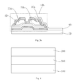
Referring to FIG. 2, the embodiment provides an array substrate which includes a glass substrate 20 and a plurality of pixel structures 10 (FIG. 2 shows exemplary part sectioned view of a pixel structure 10 therein) formed on the glass substrate 20, wherein the pixel structure 10 includes a light transmitting region 10 a and a light non-transmitting region 10 b. Herein, the light non-transmitting region 10 b includes a gate electrode 30, a gate insulating layer 40, an active layer 50, a source electrode 70 a, a drain electrode 70 b, and a passivation layer 80 sequentially formed on the glass substrate 20. The light transmitting region 10 a includes a pixel electrode 90 which is directly formed on the glass substrate 20, and the pixel electrode 90 extends to the light non-transmitting region 10 b and is electrically connected to the source/ drain electrodes 70 a and 70 b (here should be understood that the pixel electrode 90 is electrically connected to one of the source electrode 70 a and the drain electrode 70 b). Furthermore, to allow the source/ drain electrodes 70 a and 70 b to be well electrically connected to the active layer 50, an ohmic contact layer 60 is provided between the active layer 50 and the source/ drain electrodes 70 a and 70 b.
Particularly, the passivation layer 80 is provided with a via hole 80 a thereon through which the pixel electrode 90 is electrically connected to the source electrode 70 a or the drain electrode 70 b.
Herein, the material of the gate insulating layer 40 can be SiNx or SiOx, and the material of the passivation layer 80 can be SiNx or SiOx.
In the above mentioned array substrate, the gate insulating layer and the passivation layer are removed from the light transmitting region, such that the pixel electrode in the light transmitting region is directly disposed on the glass substrate, thus the light transmittance of the light transmitting region in the pixel structure is increase, so as to increase the utilization of the backlight.
The preparation process of the above mentioned array substrate will be illustrated in details by referring to FIGS. 3a-3h below.
The method of preparing the array substrate comprises the following steps:
S10: preparing a gate electrode 30 on the glass substrate 20. In particular, as shown in FIGS. 3a and 3b , first of all, a layer of gate metal thin film 30 a is formed on the glass substrate 20; and then the gate metal thin film 30 a is coated with photoresist, and the photoresist of the gate pattern region is reserved by exposing and developing the photoresist; and finally, the exposed gate metal thin film 30 a is etched away and the residual photoresist is removed to form the gate electrode 30.
S20: sequentially preparing the gate insulating layer thin film 40 a, the active layer 50, the ohmic contact layer 60, and the source/ drain electrodes 70 a and 70 b on the glass substrate 20 after step S10, wherein the gate insulating layer thin film 40 a covers the light transmitting region 10 a and the light non-transmitting region 10 b of the pixel structure 10.
Particularly, referring to FIGS. 3c-3e , first of all, the gate insulating layer thin film 40 a, the active layer thin film 50 a, the ohmic contact layer thin film 60 a, and the source/drain metal thin film 70 are sequentially formed on the glass substrate 20 on which the gate electrode 30 is formed, wherein the source/drain metal thin film 70 is coated with photoresist (not show in the figure), as shown in FIG. 3 c.
Then, the photoresist is exposed and developed with a double-tone mask, and the photoresist corresponding to a source region 70 a and a drain region 70 b, and the photoresist corresponding to a channel region are retained; and the exposed source/drain metal thin film 70, the ohmic contact layer thin film 60 a and the active layer thin film 50 a are etched away to obtain the structure shown in FIG. 3 d.
Finally, the photoresist corresponding to the channel region is removed through ashing process, the ohmic contact layer thin film 60 a and the source/drain metal thin film 70 above the channel region are etched, and the residual photoresist is removed to get the gate insulating thin film 40 a, the active layer 50, the ohmic contact layer 60 and the source/ drain electrodes 70 a and 70 b, as shown in FIG. 3 e.
S30: preparing a passivation layer thin film 80 b on the glass substrate 20 after step S20, wherein the passivation layer thin film 80 b covers the light transmitting region 10 a and the light non-transmitting region 10 b of the pixel structure 10, as shown in FIG. 3f .
S40: preparing a via hole 80 a on the passivation layer thin film 80 b by etching process to expose the source electrode 70 a or the drain electrode 70 b electrically connected to the pixel electrode 90; at the same time, etching away the gate insulating layer thin film 40 a and the passivation layer thin film 80 b of the light transmitting region 10 a, such that the light transmitting region 10 a exposes the glass substrate 20 so obtain the final gate insulating layer 40 and the passivation layer 80. Particularly, the passivation thin film 80 b is coated with photoresist, and the passivation thin film 80 b is exposed on a via hole region 80 a and the light transmitting region 10 a by exposing and developing the photoresist; the passivation layer thin film 80 b is removed from the via hole region 80 a through etching process to obtain the via hole 80 a; and then the light transmitting region 10 a exposes the glass substrate 20 by etching away the passivation layer thin film 80 b and the gate insulating layer thin film 40 a, as shown in FIG. 3g .
S50: preparing the pixel electrode 90 on the glass substrate 20 after step S40, wherein the pixel electrode 90 in the light transmitting region 10 a is directly connected to glass substrate 20, and the pixel electrode 90 is electrically connected to the source electrode 70 a or drain electrode 70 b through the via hole 80 a, as shown in FIG. 3 h.
As for the above preparation process, through one-mask process in step S40, the gate insulating layer thin film and the passivation layer thin film covered on the light transmitting region are etched away when preparing the via hole, no extra process is required, and the process is simple and easy-implementation, and in the end, an array substrate having higher transmittance is prepared.
An embodiment of the present invention also provides a liquid crystal panel, as shown in FIG. 4, the liquid crystal panel includes an array substrate 100 and a color filter substrate 200 disposed opposite to each other, and a liquid crystal layer 300 between the array substrate 100 and the color filter substrate 200, wherein the array substrate 100 uses the array substrate provided in the embodiment.
In conclusion, the array substrate and the liquid crystal panel provided according to the embodiments of the present invention improve the pixel structure in the array substrate by removing the gate insulating layer and the passivation layer in the light transmitting region, such that the pixel electrode in the light transmitting region is directly disposed on the glass substrate, to thereby increase the light transmittance of the light transmitting region in the pixel structure, and increase the utilization of the backlight.
It should be explained that the relationship terms, such as first and second, etc., in the present text are only used for distinguishing one entity or operation from another entity or operation without requiring or implying any actual relation or sequence existing between these entities or operations. Moreover, the term “include”, “contain” or any other variant means covering instead of exclusively including, so that the process, method, object or device including a series of factors not only includes those factors but also includes other factors that are not explicitly listed or further include inherent factors for this process, method, object or device. Where no more limitations are provided, the factors defined by the sentence “include one . . . ” do not exclude additional identical factors existing in the process, method, object or device which includes the factors.
The above statements are only the specific embodiments of the present application, it should be pointed out that, to those ordinary skilled in the art, several improvements and polish can be made without departing from the principle of the present application, also those improvements and polish should be considered as the protection scope of the present application.

Claims (15)

The invention claimed is:
1. An array substrate, comprises a glass substrate and a plurality of pixel structures formed on the glass substrate, each pixel structure includes a light transmitting region and a light non-transmitting region, wherein the light non-transmitting region comprises a gate electrode, a gate insulating layer, an active layer, a source electrode, a drain electrode and a passivation layer which are sequentially formed on the glass substrate;
the light transmitting region includes a pixel electrode which is directly formed on the glass substrate, and the pixel electrode extends to the light non-transmitting region and is electrically connected to the source electrode or the drain electrode, wherein the gate insulating layer, the active layer, and the source and drain electrodes are sequentially formed on both the light transmitting and non-transmitting regions of the glass substrate following a preparation of the gate electrode, such that the gate insulating layer thin film covers the light transmitting and non-transmitting regions, wherein the source/drain metal thin film is coated with a photoresist subsequently exposed and developed with a double-tone mask to retain the photoresist corresponding to a source region, a drain region, and a channel region, wherein the exposed region of the source/drain metal thin film, the ohmic contact layer thin film, and the active layer thin film are subsequently etched away and the photoresist corresponding to the channel region is removed through the ashing process, and wherein the ohmic contact layer thin film and the source/drain metal thin film on the channel region are subsequently etched and the residual photoresist is removed to obtain the gate insulating layer thin film, the active layer, the ohmic contact layer and the source/drain electrodes.
2. The array substrate of claim 1, wherein a via hole is provided on the passivation layer and through which the pixel electrode is electrically connected to the source electrode or the drain electrode.
3. The array substrate of claim 1, wherein an ohmic contact layer is provided between the active layer and the source/drain electrodes.
4. The array substrate of claim 1, wherein the material of the gate insulating layer is SiNx or SiOx.
5. The array substrate of claim 1, wherein the material of the passivation layer is SiNx or SiOx.
6. A method of preparing an array substrate, comprising:
S10: preparing a gate electrode on a glass substrate;
S20: sequentially forming a gate insulating layer thin film, an active layer, an ohmic contact layer, a source electrode and a drain electrode on the glass substrate after the step S10, wherein the gate insulating layer thin film covers a light transmitting region and a light non-transmitting region of a pixel structure,
coating a photoresist on the source/drain metal thin film, exposing and developing the photoresist with a double-tone mask, and retaining the photoresist corresponding to a source region and a drain region, and the photoresist corresponding to a channel region, etching away the exposed region of the source/drain metal thin film, the ohmic contact layer thin film and the active layer thin film, removing the photoresist corresponding to the channel region through ashing process, and etching the ohmic contact layer thin film and the source/drain metal thin film on the channel region, and removing the residual photoresist to obtain the gate insulating layer thin film, the active layer, the ohmic contact layer and the source/drain electrodes;
S30: preparing a passivation layer thin film on the glass substrate after step S20, wherein the passivation layer thin film covers the light transmitting region and the light non-transmitting region of the pixel structure;
S40: preparing a via hole on the passivation layer thin film by etching process, and etching the gate insulating layer thin film and the passivation layer thin film covered on the light transmitting region, such that the light transmitting region exposes the glass substrate; and
S50: preparing a pixel electrode on the glass substrate after step S40, wherein the pixel electrode in the light transmitting region is directly formed on the glass substrate, and the pixel electrode is electrically connected to the source electrode or the drain electrode through the via hole.
7. The method of preparing the array substrate of claim 6, wherein the step S10 specifically comprises:
forming a layer of gate metal thin film on the glass substrate;
coating a photoresist on the gate metal thin film and reserving the photoresist of a gate pattern region by exposing and developing the photoresist; and
etching away the exposed gate metal thin film and removing the residual photoresist so as to form the gate electrode.
8. The method of preparing the array substrate of claim 6, wherein the step S40 specifically comprises:
coating photoresist on the passivation layer thin film, and exposing the passivation layer thin film on a via hole region and the light transmitting region by exposing and developing the photoresist;
etching away the passivation layer thin film from the via hole region through etching process, so as to obtain the via hole; and at the same time etching away the passivation layer thin film and the gate insulating layer thin film from the light transmitting region, so as to expose the glass substrate.
9. The method of preparing the array substrate of claim 6, wherein the material of the gate insulating layer thin film is SiNx or SiOx.
10. The method of preparing the array substrate of claim 6, wherein the material of the passivation layer thin film is SiNx or SiOx.
11. A liquid crystal panel, comprising: an array substrate and a color filter substrate disposed opposite to each other, and a liquid crystal layer disposed between the array substrate and the color filter substrate, wherein the array substrate comprises a glass substrate and a plurality of pixel structures formed on the glass substrate, each pixel structure includes a light transmitting region comprising a gate electrode, a gate insulating layer, an active layer, a source electrode, a drain electrode and a passivation layer which are sequentially formed on the glass substrate and a light transmitting region including a pixel electrode formed directly on the glass substrate, and extending to the light non-transmitting region to electrically connect to the source electrode or the drain electrode, wherein the gate insulating layer, the active layer, and the source and drain electrodes are sequentially formed on both the light transmitting and non-transmitting regions of the glass substrate following a preparation of the gate electrode, such that the gate insulating layer thin film covers the light transmitting and non-transmitting regions, wherein the source/drain metal thin film is coated with a photoresist subsequently exposed and developed with a double-tone mask to retain the photoresist corresponding to a source region, a drain region, and a channel region, wherein the exposed region of the source/drain metal thin film, the ohmic contact layer thin film, and the active layer thin film are subsequently etched away and the photoresist corresponding to the channel region is removed through the ashing process, and wherein the ohmic contact layer thin film and the source/drain metal thin film on the channel region are subsequently etched and the residual photoresist is removed to obtain the gate insulating layer thin film, the active layer, the ohmic contact layer and the source/drain electrodes.
12. The liquid crystal panel of claim 11, wherein a via hole is provided on the passivation layer and through which the pixel electrode is electrically connected to the source electrode or the drain electrode.
13. The liquid crystal panel of claim 11, wherein an ohmic contact layer is provided between the active layer and the source/drain electrodes.
14. The liquid crystal panel of claim 11, wherein the material of the gate insulating layer is SiNx or SiOx.
15. The liquid crystal panel of claim 11, wherein the material of the passivation layer is SiNx or SiOx.
US14/777,876 2015-04-09 2015-04-27 Array substrate and method for preparing the same, liquid crystal panel Expired - Fee Related US9804464B2 (en)

Applications Claiming Priority (4)

Application Number Priority Date Filing Date Title
CN201510166113.3 2015-04-09
CN201510166113 2015-04-09
CN201510166113.3A CN104779256B (en) 2015-04-09 2015-04-09 Array substrate and preparation method thereof, liquid crystal display panel
PCT/CN2015/077556 WO2016161672A1 (en) 2015-04-09 2015-04-27 Array substrate and preparation method therefor, and liquid crystal panel

Publications (2)

Publication Number Publication Date
US20170108722A1 US20170108722A1 (en) 2017-04-20
US9804464B2 true US9804464B2 (en) 2017-10-31

Family

ID=53620632

Family Applications (1)

Application Number Title Priority Date Filing Date
US14/777,876 Expired - Fee Related US9804464B2 (en) 2015-04-09 2015-04-27 Array substrate and method for preparing the same, liquid crystal panel

Country Status (3)

Country Link
US (1) US9804464B2 (en)
CN (1) CN104779256B (en)
WO (1) WO2016161672A1 (en)

Cited By (1)

* Cited by examiner, † Cited by third party
Publication number Priority date Publication date Assignee Title
US20210233943A1 (en) * 2019-06-11 2021-07-29 HKC Corporation Limited Manufacture method of array substrate, array substrate, and display panel

Families Citing this family (8)

* Cited by examiner, † Cited by third party
Publication number Priority date Publication date Assignee Title
CN105093667A (en) 2015-09-25 2015-11-25 京东方科技集团股份有限公司 Array substrate, making method thereof and display device
KR102402599B1 (en) * 2015-12-16 2022-05-26 삼성디스플레이 주식회사 Transistor array panel and manufacturing method thereof
CN105914212B (en) * 2016-05-09 2019-02-05 京东方科技集团股份有限公司 Array substrate, method for making the same, and display device
CN107134432B (en) 2017-04-24 2020-02-07 惠科股份有限公司 Array substrate manufacturing process
CN107121820A (en) * 2017-07-03 2017-09-01 厦门天马微电子有限公司 A kind of liquid crystal display panel and display device
CN109471307A (en) * 2018-09-11 2019-03-15 惠科股份有限公司 Display panel and manufacturing method of first substrate of display panel
CN119922978A (en) * 2023-10-26 2025-05-02 京东方科技集团股份有限公司 Array substrate, display panel and display device
CN119861514A (en) * 2024-12-31 2025-04-22 惠科股份有限公司 Manufacturing method of array substrate, display panel and display device

Citations (6)

* Cited by examiner, † Cited by third party
Publication number Priority date Publication date Assignee Title
US5668379A (en) * 1994-07-27 1997-09-16 Hitachi, Ltd. Active matrix crystal display apparatus using thin film transistor
US20020093016A1 (en) 2000-12-06 2002-07-18 Byoung-Ho Lim Thin film transistor array substrate for liquid crystal display and a method for fabricating the same
CN101807550A (en) 2009-02-18 2010-08-18 北京京东方光电科技有限公司 Array substrate and manufacturing method thereof and LCD monitor
US20110075086A1 (en) 2009-09-30 2011-03-31 Mungi Park Liquid crystal display and fabricating method thereof
CN201867561U (en) 2010-11-09 2011-06-15 北京京东方光电科技有限公司 Array substrate and liquid crystal display
CN103149760A (en) 2013-02-19 2013-06-12 合肥京东方光电科技有限公司 Thin film transistor array substrate, manufacturing method and display device

Patent Citations (11)

* Cited by examiner, † Cited by third party
Publication number Priority date Publication date Assignee Title
US5668379A (en) * 1994-07-27 1997-09-16 Hitachi, Ltd. Active matrix crystal display apparatus using thin film transistor
US20020093016A1 (en) 2000-12-06 2002-07-18 Byoung-Ho Lim Thin film transistor array substrate for liquid crystal display and a method for fabricating the same
CN101807550A (en) 2009-02-18 2010-08-18 北京京东方光电科技有限公司 Array substrate and manufacturing method thereof and LCD monitor
US8553184B2 (en) 2009-02-18 2013-10-08 Beijing Boe Optoelectronics Technology Co., Ltd. Manufacturing method of an array substrate including a four step process
US20110075086A1 (en) 2009-09-30 2011-03-31 Mungi Park Liquid crystal display and fabricating method thereof
CN102033375A (en) 2009-09-30 2011-04-27 乐金显示有限公司 Liquid crystal display and fabricating method thereof
US8817214B2 (en) 2009-09-30 2014-08-26 Lg Display Co., Ltd. Liquid crystal display and fabricating method thereof
CN201867561U (en) 2010-11-09 2011-06-15 北京京东方光电科技有限公司 Array substrate and liquid crystal display
US8860898B2 (en) 2010-11-09 2014-10-14 Beijing Boe Optoelectronics Technology Co., Ltd. Array substrate and liquid crystal display
CN103149760A (en) 2013-02-19 2013-06-12 合肥京东方光电科技有限公司 Thin film transistor array substrate, manufacturing method and display device
US20160141314A1 (en) 2013-02-19 2016-05-19 Boe Technology Group Co., Ltd. Thin film transistor array substrate, manufacturing method and display device

Non-Patent Citations (1)

* Cited by examiner, † Cited by third party
Title
International Search Report for PCT/CN2015/077556, English translation attached to original, Both completed by the Chinese Patent Office dated Dec. 15, 2015, All together 6 Pages.

Cited By (2)

* Cited by examiner, † Cited by third party
Publication number Priority date Publication date Assignee Title
US20210233943A1 (en) * 2019-06-11 2021-07-29 HKC Corporation Limited Manufacture method of array substrate, array substrate, and display panel
US11961852B2 (en) * 2019-06-11 2024-04-16 HKC Corporation Limited Manufacture method of array substrate, array substrate, and display panel

Also Published As

Publication number Publication date
CN104779256A (en) 2015-07-15
US20170108722A1 (en) 2017-04-20
WO2016161672A1 (en) 2016-10-13
CN104779256B (en) 2018-08-24

Similar Documents

Publication Publication Date Title
US9804464B2 (en) Array substrate and method for preparing the same, liquid crystal panel
US9709864B2 (en) Array substrate and its manufacturing method and display device
US10128281B2 (en) Array substrate, fabrication method thereof and display device
US6204081B1 (en) Method for manufacturing a substrate of a liquid crystal display device
EP3054483A1 (en) Array substrate, manufacturing method therefor, and display apparatus
WO2017054384A1 (en) Array substrate, manufacturing method therefor and display panel
CN104576659A (en) Array substrate and manufacturing method thereof as well as display device
US11049889B2 (en) Method for preparing array substrate by stripping first photo-resist layer through wet etching before forming ohm contact layer and active layer
US10509286B2 (en) Pixel structure and manufacturing method thereof, array substrate and display apparatus
US9305945B2 (en) TFT array substrate, manufacturing method of the same and display device
US20180158953A1 (en) Array substrate and method for manufacturing the same
CN103489874B (en) Array base palte and preparation method thereof, display unit
US8537327B2 (en) Array substrate and manufacturing method thereof, liquid crystal display
WO2015180357A1 (en) Array substrate and manufacturing method therefor, and display device
US20140071553A1 (en) Color filter substrate, tft array substrate, manufacturing method of the same, and liquid crystal display panel
KR100288150B1 (en) Method of Fabricating Liquid Crystal Display
US10649291B2 (en) Array substrate and method for manufacturing the same, display panel and display apparatus
US9263483B2 (en) Array panel and manufacturing method for the same
US10497906B2 (en) Manufacturing method of thin film transistor array substrate
US6521491B2 (en) Method for fabricating thin film transistor-liquid crystal display
CN105789121A (en) Total reflection array substrate and preparation method thereof and display device
US9780120B2 (en) Method for manufacturing array substrate, array substrate thereof and display device
KR100527086B1 (en) Method for manufacturing liquid crystal display device
US10355026B2 (en) Method for manufacturing metal wire and array substrate using the same
US5916737A (en) Method for fabricating liquid crystal display device

Legal Events

Date Code Title Description
AS Assignment

Owner name: SHENZHEN CHINA STAR OPTOELECTRONICS TECHNOLOGY CO.

Free format text: ASSIGNMENT OF ASSIGNORS INTEREST;ASSIGNOR:GAO, DONGZI;REEL/FRAME:036591/0130

Effective date: 20150916

STCF Information on status: patent grant

Free format text: PATENTED CASE

MAFP Maintenance fee payment

Free format text: PAYMENT OF MAINTENANCE FEE, 4TH YEAR, LARGE ENTITY (ORIGINAL EVENT CODE: M1551); ENTITY STATUS OF PATENT OWNER: LARGE ENTITY

Year of fee payment: 4

FEPP Fee payment procedure

Free format text: MAINTENANCE FEE REMINDER MAILED (ORIGINAL EVENT CODE: REM.); ENTITY STATUS OF PATENT OWNER: LARGE ENTITY

LAPS Lapse for failure to pay maintenance fees

Free format text: PATENT EXPIRED FOR FAILURE TO PAY MAINTENANCE FEES (ORIGINAL EVENT CODE: EXP.); ENTITY STATUS OF PATENT OWNER: LARGE ENTITY

STCH Information on status: patent discontinuation

Free format text: PATENT EXPIRED DUE TO NONPAYMENT OF MAINTENANCE FEES UNDER 37 CFR 1.362

FP Lapsed due to failure to pay maintenance fee

Effective date: 20251031