US9800213B1 - Amplifier devices with impedance matching networks that incorporate a capacitor integrated with a bond pad - Google Patents
Amplifier devices with impedance matching networks that incorporate a capacitor integrated with a bond pad Download PDFInfo
- Publication number
- US9800213B1 US9800213B1 US15/187,376 US201615187376A US9800213B1 US 9800213 B1 US9800213 B1 US 9800213B1 US 201615187376 A US201615187376 A US 201615187376A US 9800213 B1 US9800213 B1 US 9800213B1
- Authority
- US
- United States
- Prior art keywords
- bond pad
- amplifier
- capacitor
- plate
- impedance matching
- Prior art date
- Legal status (The legal status is an assumption and is not a legal conclusion. Google has not performed a legal analysis and makes no representation as to the accuracy of the status listed.)
- Active
Links
Images


Classifications
-
- H—ELECTRICITY
- H03—ELECTRONIC CIRCUITRY
- H03F—AMPLIFIERS
- H03F1/00—Details of amplifiers with only discharge tubes, only semiconductor devices or only unspecified devices as amplifying elements
- H03F1/56—Modifications of input or output impedances, not otherwise provided for
-
- H—ELECTRICITY
- H03—ELECTRONIC CIRCUITRY
- H03F—AMPLIFIERS
- H03F3/00—Amplifiers with only discharge tubes or only semiconductor devices as amplifying elements
- H03F3/189—High frequency amplifiers, e.g. radio frequency amplifiers
- H03F3/19—High frequency amplifiers, e.g. radio frequency amplifiers with semiconductor devices only
- H03F3/195—High frequency amplifiers, e.g. radio frequency amplifiers with semiconductor devices only in integrated circuits
-
- H—ELECTRICITY
- H01—ELECTRIC ELEMENTS
- H01L—SEMICONDUCTOR DEVICES NOT COVERED BY CLASS H10
- H01L23/00—Details of semiconductor or other solid state devices
- H01L23/52—Arrangements for conducting electric current within the device in operation from one component to another, i.e. interconnections, e.g. wires, lead frames
- H01L23/522—Arrangements for conducting electric current within the device in operation from one component to another, i.e. interconnections, e.g. wires, lead frames including external interconnections consisting of a multilayer structure of conductive and insulating layers inseparably formed on the semiconductor body
- H01L23/5222—Capacitive arrangements or effects of, or between wiring layers
- H01L23/5223—Capacitor integral with wiring layers
-
- H—ELECTRICITY
- H01—ELECTRIC ELEMENTS
- H01L—SEMICONDUCTOR DEVICES NOT COVERED BY CLASS H10
- H01L23/00—Details of semiconductor or other solid state devices
- H01L23/58—Structural electrical arrangements for semiconductor devices not otherwise provided for, e.g. in combination with batteries
- H01L23/64—Impedance arrangements
- H01L23/66—High-frequency adaptations
-
- H—ELECTRICITY
- H03—ELECTRONIC CIRCUITRY
- H03F—AMPLIFIERS
- H03F1/00—Details of amplifiers with only discharge tubes, only semiconductor devices or only unspecified devices as amplifying elements
- H03F1/56—Modifications of input or output impedances, not otherwise provided for
- H03F1/565—Modifications of input or output impedances, not otherwise provided for using inductive elements
-
- H—ELECTRICITY
- H03—ELECTRONIC CIRCUITRY
- H03F—AMPLIFIERS
- H03F3/00—Amplifiers with only discharge tubes or only semiconductor devices as amplifying elements
- H03F3/189—High frequency amplifiers, e.g. radio frequency amplifiers
- H03F3/19—High frequency amplifiers, e.g. radio frequency amplifiers with semiconductor devices only
- H03F3/193—High frequency amplifiers, e.g. radio frequency amplifiers with semiconductor devices only with field-effect devices
-
- H—ELECTRICITY
- H01—ELECTRIC ELEMENTS
- H01L—SEMICONDUCTOR DEVICES NOT COVERED BY CLASS H10
- H01L2223/00—Details relating to semiconductor or other solid state devices covered by the group H01L23/00
- H01L2223/58—Structural electrical arrangements for semiconductor devices not otherwise provided for
- H01L2223/64—Impedance arrangements
- H01L2223/66—High-frequency adaptations
- H01L2223/6605—High-frequency electrical connections
- H01L2223/6611—Wire connections
-
- H—ELECTRICITY
- H01—ELECTRIC ELEMENTS
- H01L—SEMICONDUCTOR DEVICES NOT COVERED BY CLASS H10
- H01L2223/00—Details relating to semiconductor or other solid state devices covered by the group H01L23/00
- H01L2223/58—Structural electrical arrangements for semiconductor devices not otherwise provided for
- H01L2223/64—Impedance arrangements
- H01L2223/66—High-frequency adaptations
- H01L2223/6644—Packaging aspects of high-frequency amplifiers
- H01L2223/6655—Matching arrangements, e.g. arrangement of inductive and capacitive components
-
- H—ELECTRICITY
- H01—ELECTRIC ELEMENTS
- H01L—SEMICONDUCTOR DEVICES NOT COVERED BY CLASS H10
- H01L2224/00—Indexing scheme for arrangements for connecting or disconnecting semiconductor or solid-state bodies and methods related thereto as covered by H01L24/00
- H01L2224/01—Means for bonding being attached to, or being formed on, the surface to be connected, e.g. chip-to-package, die-attach, "first-level" interconnects; Manufacturing methods related thereto
- H01L2224/02—Bonding areas; Manufacturing methods related thereto
- H01L2224/0212—Auxiliary members for bonding areas, e.g. spacers
- H01L2224/02122—Auxiliary members for bonding areas, e.g. spacers being formed on the semiconductor or solid-state body
- H01L2224/02163—Auxiliary members for bonding areas, e.g. spacers being formed on the semiconductor or solid-state body on the bonding area
- H01L2224/02165—Reinforcing structures
- H01L2224/02166—Collar structures
-
- H—ELECTRICITY
- H01—ELECTRIC ELEMENTS
- H01L—SEMICONDUCTOR DEVICES NOT COVERED BY CLASS H10
- H01L2224/00—Indexing scheme for arrangements for connecting or disconnecting semiconductor or solid-state bodies and methods related thereto as covered by H01L24/00
- H01L2224/01—Means for bonding being attached to, or being formed on, the surface to be connected, e.g. chip-to-package, die-attach, "first-level" interconnects; Manufacturing methods related thereto
- H01L2224/02—Bonding areas; Manufacturing methods related thereto
- H01L2224/04—Structure, shape, material or disposition of the bonding areas prior to the connecting process
- H01L2224/0401—Bonding areas specifically adapted for bump connectors, e.g. under bump metallisation [UBM]
-
- H—ELECTRICITY
- H01—ELECTRIC ELEMENTS
- H01L—SEMICONDUCTOR DEVICES NOT COVERED BY CLASS H10
- H01L2224/00—Indexing scheme for arrangements for connecting or disconnecting semiconductor or solid-state bodies and methods related thereto as covered by H01L24/00
- H01L2224/01—Means for bonding being attached to, or being formed on, the surface to be connected, e.g. chip-to-package, die-attach, "first-level" interconnects; Manufacturing methods related thereto
- H01L2224/02—Bonding areas; Manufacturing methods related thereto
- H01L2224/04—Structure, shape, material or disposition of the bonding areas prior to the connecting process
- H01L2224/04042—Bonding areas specifically adapted for wire connectors, e.g. wirebond pads
-
- H—ELECTRICITY
- H01—ELECTRIC ELEMENTS
- H01L—SEMICONDUCTOR DEVICES NOT COVERED BY CLASS H10
- H01L2224/00—Indexing scheme for arrangements for connecting or disconnecting semiconductor or solid-state bodies and methods related thereto as covered by H01L24/00
- H01L2224/01—Means for bonding being attached to, or being formed on, the surface to be connected, e.g. chip-to-package, die-attach, "first-level" interconnects; Manufacturing methods related thereto
- H01L2224/02—Bonding areas; Manufacturing methods related thereto
- H01L2224/04—Structure, shape, material or disposition of the bonding areas prior to the connecting process
- H01L2224/05—Structure, shape, material or disposition of the bonding areas prior to the connecting process of an individual bonding area
- H01L2224/0554—External layer
- H01L2224/0556—Disposition
- H01L2224/05567—Disposition the external layer being at least partially embedded in the surface
-
- H—ELECTRICITY
- H01—ELECTRIC ELEMENTS
- H01L—SEMICONDUCTOR DEVICES NOT COVERED BY CLASS H10
- H01L2224/00—Indexing scheme for arrangements for connecting or disconnecting semiconductor or solid-state bodies and methods related thereto as covered by H01L24/00
- H01L2224/01—Means for bonding being attached to, or being formed on, the surface to be connected, e.g. chip-to-package, die-attach, "first-level" interconnects; Manufacturing methods related thereto
- H01L2224/02—Bonding areas; Manufacturing methods related thereto
- H01L2224/04—Structure, shape, material or disposition of the bonding areas prior to the connecting process
- H01L2224/05—Structure, shape, material or disposition of the bonding areas prior to the connecting process of an individual bonding area
- H01L2224/0554—External layer
- H01L2224/05599—Material
- H01L2224/056—Material with a principal constituent of the material being a metal or a metalloid, e.g. boron [B], silicon [Si], germanium [Ge], arsenic [As], antimony [Sb], tellurium [Te] and polonium [Po], and alloys thereof
- H01L2224/05638—Material with a principal constituent of the material being a metal or a metalloid, e.g. boron [B], silicon [Si], germanium [Ge], arsenic [As], antimony [Sb], tellurium [Te] and polonium [Po], and alloys thereof the principal constituent melting at a temperature of greater than or equal to 950°C and less than 1550°C
- H01L2224/05647—Copper [Cu] as principal constituent
-
- H—ELECTRICITY
- H01—ELECTRIC ELEMENTS
- H01L—SEMICONDUCTOR DEVICES NOT COVERED BY CLASS H10
- H01L2224/00—Indexing scheme for arrangements for connecting or disconnecting semiconductor or solid-state bodies and methods related thereto as covered by H01L24/00
- H01L2224/01—Means for bonding being attached to, or being formed on, the surface to be connected, e.g. chip-to-package, die-attach, "first-level" interconnects; Manufacturing methods related thereto
- H01L2224/10—Bump connectors; Manufacturing methods related thereto
- H01L2224/12—Structure, shape, material or disposition of the bump connectors prior to the connecting process
- H01L2224/13—Structure, shape, material or disposition of the bump connectors prior to the connecting process of an individual bump connector
- H01L2224/13001—Core members of the bump connector
- H01L2224/13099—Material
- H01L2224/131—Material with a principal constituent of the material being a metal or a metalloid, e.g. boron [B], silicon [Si], germanium [Ge], arsenic [As], antimony [Sb], tellurium [Te] and polonium [Po], and alloys thereof
-
- H—ELECTRICITY
- H01—ELECTRIC ELEMENTS
- H01L—SEMICONDUCTOR DEVICES NOT COVERED BY CLASS H10
- H01L2224/00—Indexing scheme for arrangements for connecting or disconnecting semiconductor or solid-state bodies and methods related thereto as covered by H01L24/00
- H01L2224/01—Means for bonding being attached to, or being formed on, the surface to be connected, e.g. chip-to-package, die-attach, "first-level" interconnects; Manufacturing methods related thereto
- H01L2224/10—Bump connectors; Manufacturing methods related thereto
- H01L2224/15—Structure, shape, material or disposition of the bump connectors after the connecting process
- H01L2224/16—Structure, shape, material or disposition of the bump connectors after the connecting process of an individual bump connector
- H01L2224/161—Disposition
- H01L2224/16151—Disposition the bump connector connecting between a semiconductor or solid-state body and an item not being a semiconductor or solid-state body, e.g. chip-to-substrate, chip-to-passive
- H01L2224/16221—Disposition the bump connector connecting between a semiconductor or solid-state body and an item not being a semiconductor or solid-state body, e.g. chip-to-substrate, chip-to-passive the body and the item being stacked
- H01L2224/16225—Disposition the bump connector connecting between a semiconductor or solid-state body and an item not being a semiconductor or solid-state body, e.g. chip-to-substrate, chip-to-passive the body and the item being stacked the item being non-metallic, e.g. insulating substrate with or without metallisation
- H01L2224/16227—Disposition the bump connector connecting between a semiconductor or solid-state body and an item not being a semiconductor or solid-state body, e.g. chip-to-substrate, chip-to-passive the body and the item being stacked the item being non-metallic, e.g. insulating substrate with or without metallisation the bump connector connecting to a bond pad of the item
-
- H—ELECTRICITY
- H01—ELECTRIC ELEMENTS
- H01L—SEMICONDUCTOR DEVICES NOT COVERED BY CLASS H10
- H01L2224/00—Indexing scheme for arrangements for connecting or disconnecting semiconductor or solid-state bodies and methods related thereto as covered by H01L24/00
- H01L2224/01—Means for bonding being attached to, or being formed on, the surface to be connected, e.g. chip-to-package, die-attach, "first-level" interconnects; Manufacturing methods related thereto
- H01L2224/42—Wire connectors; Manufacturing methods related thereto
- H01L2224/47—Structure, shape, material or disposition of the wire connectors after the connecting process
- H01L2224/48—Structure, shape, material or disposition of the wire connectors after the connecting process of an individual wire connector
- H01L2224/4805—Shape
- H01L2224/4809—Loop shape
- H01L2224/48091—Arched
-
- H—ELECTRICITY
- H01—ELECTRIC ELEMENTS
- H01L—SEMICONDUCTOR DEVICES NOT COVERED BY CLASS H10
- H01L2224/00—Indexing scheme for arrangements for connecting or disconnecting semiconductor or solid-state bodies and methods related thereto as covered by H01L24/00
- H01L2224/01—Means for bonding being attached to, or being formed on, the surface to be connected, e.g. chip-to-package, die-attach, "first-level" interconnects; Manufacturing methods related thereto
- H01L2224/42—Wire connectors; Manufacturing methods related thereto
- H01L2224/47—Structure, shape, material or disposition of the wire connectors after the connecting process
- H01L2224/48—Structure, shape, material or disposition of the wire connectors after the connecting process of an individual wire connector
- H01L2224/481—Disposition
- H01L2224/48135—Connecting between different semiconductor or solid-state bodies, i.e. chip-to-chip
- H01L2224/48137—Connecting between different semiconductor or solid-state bodies, i.e. chip-to-chip the bodies being arranged next to each other, e.g. on a common substrate
-
- H—ELECTRICITY
- H01—ELECTRIC ELEMENTS
- H01L—SEMICONDUCTOR DEVICES NOT COVERED BY CLASS H10
- H01L2224/00—Indexing scheme for arrangements for connecting or disconnecting semiconductor or solid-state bodies and methods related thereto as covered by H01L24/00
- H01L2224/01—Means for bonding being attached to, or being formed on, the surface to be connected, e.g. chip-to-package, die-attach, "first-level" interconnects; Manufacturing methods related thereto
- H01L2224/42—Wire connectors; Manufacturing methods related thereto
- H01L2224/47—Structure, shape, material or disposition of the wire connectors after the connecting process
- H01L2224/48—Structure, shape, material or disposition of the wire connectors after the connecting process of an individual wire connector
- H01L2224/481—Disposition
- H01L2224/48151—Connecting between a semiconductor or solid-state body and an item not being a semiconductor or solid-state body, e.g. chip-to-substrate, chip-to-passive
- H01L2224/48221—Connecting between a semiconductor or solid-state body and an item not being a semiconductor or solid-state body, e.g. chip-to-substrate, chip-to-passive the body and the item being stacked
- H01L2224/48225—Connecting between a semiconductor or solid-state body and an item not being a semiconductor or solid-state body, e.g. chip-to-substrate, chip-to-passive the body and the item being stacked the item being non-metallic, e.g. insulating substrate with or without metallisation
- H01L2224/48227—Connecting between a semiconductor or solid-state body and an item not being a semiconductor or solid-state body, e.g. chip-to-substrate, chip-to-passive the body and the item being stacked the item being non-metallic, e.g. insulating substrate with or without metallisation connecting the wire to a bond pad of the item
-
- H—ELECTRICITY
- H01—ELECTRIC ELEMENTS
- H01L—SEMICONDUCTOR DEVICES NOT COVERED BY CLASS H10
- H01L2224/00—Indexing scheme for arrangements for connecting or disconnecting semiconductor or solid-state bodies and methods related thereto as covered by H01L24/00
- H01L2224/01—Means for bonding being attached to, or being formed on, the surface to be connected, e.g. chip-to-package, die-attach, "first-level" interconnects; Manufacturing methods related thereto
- H01L2224/42—Wire connectors; Manufacturing methods related thereto
- H01L2224/47—Structure, shape, material or disposition of the wire connectors after the connecting process
- H01L2224/48—Structure, shape, material or disposition of the wire connectors after the connecting process of an individual wire connector
- H01L2224/484—Connecting portions
- H01L2224/48463—Connecting portions the connecting portion on the bonding area of the semiconductor or solid-state body being a ball bond
-
- H—ELECTRICITY
- H01—ELECTRIC ELEMENTS
- H01L—SEMICONDUCTOR DEVICES NOT COVERED BY CLASS H10
- H01L2224/00—Indexing scheme for arrangements for connecting or disconnecting semiconductor or solid-state bodies and methods related thereto as covered by H01L24/00
- H01L2224/01—Means for bonding being attached to, or being formed on, the surface to be connected, e.g. chip-to-package, die-attach, "first-level" interconnects; Manufacturing methods related thereto
- H01L2224/42—Wire connectors; Manufacturing methods related thereto
- H01L2224/47—Structure, shape, material or disposition of the wire connectors after the connecting process
- H01L2224/48—Structure, shape, material or disposition of the wire connectors after the connecting process of an individual wire connector
- H01L2224/484—Connecting portions
- H01L2224/4847—Connecting portions the connecting portion on the bonding area of the semiconductor or solid-state body being a wedge bond
-
- H—ELECTRICITY
- H01—ELECTRIC ELEMENTS
- H01L—SEMICONDUCTOR DEVICES NOT COVERED BY CLASS H10
- H01L2224/00—Indexing scheme for arrangements for connecting or disconnecting semiconductor or solid-state bodies and methods related thereto as covered by H01L24/00
- H01L2224/01—Means for bonding being attached to, or being formed on, the surface to be connected, e.g. chip-to-package, die-attach, "first-level" interconnects; Manufacturing methods related thereto
- H01L2224/42—Wire connectors; Manufacturing methods related thereto
- H01L2224/47—Structure, shape, material or disposition of the wire connectors after the connecting process
- H01L2224/49—Structure, shape, material or disposition of the wire connectors after the connecting process of a plurality of wire connectors
- H01L2224/491—Disposition
- H01L2224/4911—Disposition the connectors being bonded to at least one common bonding area, e.g. daisy chain
-
- H—ELECTRICITY
- H01—ELECTRIC ELEMENTS
- H01L—SEMICONDUCTOR DEVICES NOT COVERED BY CLASS H10
- H01L24/00—Arrangements for connecting or disconnecting semiconductor or solid-state bodies; Methods or apparatus related thereto
- H01L24/01—Means for bonding being attached to, or being formed on, the surface to be connected, e.g. chip-to-package, die-attach, "first-level" interconnects; Manufacturing methods related thereto
- H01L24/02—Bonding areas ; Manufacturing methods related thereto
- H01L24/04—Structure, shape, material or disposition of the bonding areas prior to the connecting process
- H01L24/05—Structure, shape, material or disposition of the bonding areas prior to the connecting process of an individual bonding area
-
- H—ELECTRICITY
- H01—ELECTRIC ELEMENTS
- H01L—SEMICONDUCTOR DEVICES NOT COVERED BY CLASS H10
- H01L24/00—Arrangements for connecting or disconnecting semiconductor or solid-state bodies; Methods or apparatus related thereto
- H01L24/01—Means for bonding being attached to, or being formed on, the surface to be connected, e.g. chip-to-package, die-attach, "first-level" interconnects; Manufacturing methods related thereto
- H01L24/10—Bump connectors ; Manufacturing methods related thereto
- H01L24/15—Structure, shape, material or disposition of the bump connectors after the connecting process
- H01L24/16—Structure, shape, material or disposition of the bump connectors after the connecting process of an individual bump connector
-
- H—ELECTRICITY
- H01—ELECTRIC ELEMENTS
- H01L—SEMICONDUCTOR DEVICES NOT COVERED BY CLASS H10
- H01L24/00—Arrangements for connecting or disconnecting semiconductor or solid-state bodies; Methods or apparatus related thereto
- H01L24/01—Means for bonding being attached to, or being formed on, the surface to be connected, e.g. chip-to-package, die-attach, "first-level" interconnects; Manufacturing methods related thereto
- H01L24/42—Wire connectors; Manufacturing methods related thereto
- H01L24/47—Structure, shape, material or disposition of the wire connectors after the connecting process
- H01L24/48—Structure, shape, material or disposition of the wire connectors after the connecting process of an individual wire connector
-
- H—ELECTRICITY
- H01—ELECTRIC ELEMENTS
- H01L—SEMICONDUCTOR DEVICES NOT COVERED BY CLASS H10
- H01L24/00—Arrangements for connecting or disconnecting semiconductor or solid-state bodies; Methods or apparatus related thereto
- H01L24/01—Means for bonding being attached to, or being formed on, the surface to be connected, e.g. chip-to-package, die-attach, "first-level" interconnects; Manufacturing methods related thereto
- H01L24/42—Wire connectors; Manufacturing methods related thereto
- H01L24/47—Structure, shape, material or disposition of the wire connectors after the connecting process
- H01L24/49—Structure, shape, material or disposition of the wire connectors after the connecting process of a plurality of wire connectors
-
- H—ELECTRICITY
- H01—ELECTRIC ELEMENTS
- H01L—SEMICONDUCTOR DEVICES NOT COVERED BY CLASS H10
- H01L2924/00—Indexing scheme for arrangements or methods for connecting or disconnecting semiconductor or solid-state bodies as covered by H01L24/00
- H01L2924/30—Technical effects
- H01L2924/301—Electrical effects
- H01L2924/30107—Inductance
-
- H—ELECTRICITY
- H01—ELECTRIC ELEMENTS
- H01L—SEMICONDUCTOR DEVICES NOT COVERED BY CLASS H10
- H01L2924/00—Indexing scheme for arrangements or methods for connecting or disconnecting semiconductor or solid-state bodies as covered by H01L24/00
- H01L2924/30—Technical effects
- H01L2924/301—Electrical effects
- H01L2924/3011—Impedance
- H01L2924/30111—Impedance matching
-
- H—ELECTRICITY
- H03—ELECTRONIC CIRCUITRY
- H03F—AMPLIFIERS
- H03F2200/00—Indexing scheme relating to amplifiers
- H03F2200/451—Indexing scheme relating to amplifiers the amplifier being a radio frequency amplifier
Definitions
- Embodiments of the subject matter described herein relate generally to amplifiers, and more particularly to radio frequency (RF) power amplifiers used in a variety of applications.
- RF radio frequency
- amplifiers are used to increase the power of signals.
- amplifiers can be used to convert low-power radio frequency (RF) signals into higher power RF signals for driving the antenna of a transmitter.
- RF radio frequency
- amplifiers may be implemented as part of an overall power amplifier used by an RF transmission system.
- bandwidth is the bandwidth of the amplifier divided by the center frequency of the amplifier. This can make it difficult to provide an amplifier with both high efficiency and high bandwidth.
- FIG. 1 is a schematic diagram of a portion of an amplifier device in accordance with an example embodiment
- FIG. 2 is a schematic diagram of a portion of an amplifier device in accordance with an example embodiment
- FIG. 3 is a schematic diagram of a portion of an amplifier device in accordance with an example embodiment
- FIG. 4 is a circuit diagram of a portion of an amplifier device in accordance with an example embodiment
- FIG. 5 is a side, cross-sectional view of a portion of a device that includes an impedance matching network in accordance with an example embodiment
- FIG. 6 is a side, cross-sectional view of a portion of a device that includes an impedance matching network in accordance with an example embodiment
- FIG. 7 is a circuit diagram of a portion of an amplifier device in accordance with an example embodiment
- FIG. 8 is a side, cross-sectional view of a portion of a device that includes an impedance matching network in accordance with an example embodiment
- FIG. 9 is a top view of a portion of a device that includes an impedance matching network in accordance with an example embodiment.
- FIG. 10 is a circuit diagram of a portion of an amplifier device in accordance with an example embodiment.
- the embodiments described herein can provide semiconductor devices, and particularly amplifiers, that may have improved performance when compared with conventional devices.
- the embodiments described herein include semiconductor devices that form portions of amplifiers that may be used in radio frequency (RF) applications.
- the semiconductor devices described herein incorporate a capacitor integrated with a bond pad into an impedance matching network for the amplifier.
- the term “bond pad capacitor” means a capacitor that includes a bond pad as a capacitor plate, or a capacitor that includes a capacitor plate that is directly electrically coupled with a bond pad. Incorporating a bond pad capacitor into an impedance matching network can reduce the negative effects of parasitic bond pad capacitance on the performance of the amplifier. In addition, implementing the bond pad capacitor into the impedance matching network can improve the bandwidth of the amplifier.
- the amplifier device 100 includes an amplifier 102 and an impedance matching network 104 .
- the impedance matching network 104 includes a bond pad capacitor 106 .
- the bond pad capacitor 106 is incorporated into the impedance matching network 104 in way that can enhance the performance of the amplifier device 100 .
- the amplifier 102 can be implemented with one or more single-stage or multi-stage power transistors formed in a semiconductor device.
- These transistors may be any suitable transistor type, including a field effect transistor (FET), such as a laterally-diffused metal oxide semiconductor (LDMOS) FET, which may be implemented using a gallium nitride (GaN), silicon, or gallium arsenide (GaAs) semiconductor device.
- FET field effect transistor
- LDMOS laterally-diffused metal oxide semiconductor
- GaN gallium nitride
- silicon silicon
- GaAs gallium arsenide
- other types of transistor devices may be used (e.g., other types of FETs, bipolar junction transistors, and so on), which may be implemented using other types of semiconductor materials.
- FET terminology will be used herein, such as describing a particular transistor as including a gate, source, and drain.
- the amplifier 102 receives an input signal from a signal source 112 (e.g., an RF signal source), and outputs an amplified signal through the impedance matching network 104 and to the load 116 .
- a signal source 112 e.g., an RF signal source
- the RF signal source 112 may be electrically coupled to the gate of the amplifier transistor
- the amplified signal may be produced at the drain (or source) of the amplifier transistor
- the source (or drain) may be coupled to a ground reference 110 .
- the gate may be referred to herein as the “input” of the amplifier.
- either the drain or the source may function to produce the amplified signal.
- the drain produces the amplified signal
- the source alternatively may produce the amplified signal (and the drain may be coupled to the ground reference 110 ).
- the transistor region that produces the amplified signal may be referred to generally herein as the “output” of the amplifier transistor.
- the impedance matching network 104 is designed and configured to facilitate efficient power transfer from the amplifier 102 to load the load 116 during such operation. To facilitate this, the impedance matching network 104 is coupled to the amplifier 102 . As will be described below, in some embodiments the impedance matching network 104 comprises an output impedance matching network coupled to the amplifier 102 output. In other embodiments, the impedance matching network 104 comprises an input impedance matching network coupled to the amplifier 102 input. In either such embodiment, the impedance matching network 104 includes a bond pad capacitor 106 , where the bond pad capacitor 106 is formed at least in part with a bond pad on a semiconductor die that includes the amplifier 102 , and wherein the bond pad is physically connected to at least one bonding wire.
- bond pad capacitor 106 can be configured in series with the amplifier 102 (i.e., with one capacitor plate coupled to the amplifier input or output, and the other capacitor plate coupled to the RF source 112 or the load 116 ). Specifically, the bond pad capacitor 106 can be configured in series with the amplifier 102 output or in series with the amplifier 102 input. Alternatively, the bond pad capacitor 106 can be configured between a ground 110 and the amplifier 102 output or between a ground 110 and the amplifier 102 input.
- the bond pad capacitor 106 can be configured to provide DC blocking to block a DC bias signal from reaching the ground. Stated another way, the bond pad capacitor 106 can be configured to additionally decouple a DC bias signal from the RF signal being amplified.
- the amplifier 102 includes one or more transistors, where those transistors are formed on a semiconductor wafer, and that wafer is then singulated into individual dies.
- Each individual die can include the transistors for one or more amplifiers (e.g., amplifier 102 ), and elements of the impedance matching networks (e.g., impedance matching network 104 ).
- such dies will also include at least one bond pad, where the bond pad is used to couple to bond wires, and where the bond pad forms at least part of the bond pad capacitor 106 .
- the amplifier 102 may be a “flip-chip” type of device, in which the electrical equivalent of a bond pad is referred to more simply as a “pad”, and solder bumps or balls make the electrical connection to external circuitry (rather than using bond wires).
- bond pad is used extensively herein, it is to be understood that the term also encompasses flip chip pads or other electrically equivalent types of connections.
- Such die(s) and other remaining elements of the impedance matching networks are then incorporated into a device package or directly coupled to a module substrate.
- the package encases the die(s) and associated components, and the package includes leads that provide the electrical connection to the encased dies and associated components.
- a typical package also includes structural components (e.g., including a flange or substrate) to which the die(s) and other primary electrical components are coupled. Electrical connections between the die(s), the other components, and the package leads can be provided by bond wires coupled to the bond pads or other suitable conductors.
- the package also may include an isolator that electrically isolates the package substrate or flange from the leads or alternatively may include encapsulation that provides such electrical isolation.
- a packaged semiconductor device When completed, a packaged semiconductor device is a distinct device that may be mounted to a printed circuit board (PCB) or other suitable substrate, thus providing electrical connectivity to other components of an amplifier system.
- PCB printed circuit board
- a typical package could include one or more amplifiers.
- such a package can include additional semiconductor devices and/or other components, including, for example, components of an impedance matching network coupled between the device's input lead and the input (e.g., the gate) of the transistor.
- Non-limiting examples of the type of packages that can be used include air cavity and over-molded packages.
- such packages can utilize a variety of different types of leads, such as gull wing leads, J-leads, pin grid arrays, ball grid arrays, land grid arrays, etc.
- the bond pad capacitor 106 is formed at least in part with a bond pad formed on a semiconductor die, where the bond pad is used to couple to bonding wires (or solder bumps or balls).
- a capacitor generally includes two conductive plates (or electrodes) that are separated by dielectric material.
- the bond pad capacitor 106 is formed in part with a bond pad that is formed in a first metallization layer, where this bond pad provides a first plate of the bond pad capacitor and where a second plate of the bond pad capacitor is formed in an underlying second metallization layer that is separated from the first metallization layer by dielectric material.
- the bond pad capacitor is embodied as a capacitor that comprises a first capacitor plate formed in the first metallization layer, where the first capacitor plate is coupled to a bond pad in an underlying second metallization layer.
- an opening in the semiconductor device is provided so that the bonding wires can be attached to the bond pad in the second metallization layer.
- the amplifier device 200 includes an amplifier 202 and an output impedance matching network 204 .
- the output impedance matching network 204 includes a bond pad capacitor 206 , and in this embodiment further includes a series inductance 220 , a shunt inductance 222 , and an additional inductance 224 .
- series inductance 220 is coupled between one plate of the bond pad capacitor 206 and a load 216 .
- shunt inductance 222 is coupled between one plate of the bond pad capacitor 206 and a ground reference 218 .
- inductance 224 is coupled between one plate of the bond pad capacitor 206 and a DC bias voltage source.
- the amplifier 202 can be implemented with one or more transistors of any suitable type. During operation, the amplifier 202 receives an RF input signal at a signal source 212 , and outputs an amplified signal through the output impedance matching network 204 and to the load 216 .
- the bond pad capacitor 206 is incorporated into the output impedance matching network 204 so that the bond pad capacitor 206 does not degrade the performance of the amplifier device 200 .
- the bond pad capacitor 206 is implemented to be in series with the amplifier 202 output, and is thus between the amplifier 202 output (e.g., the drain) and the load 216 .
- the bond pad capacitor 206 is implemented between a DC bias voltage source and the ground reference 218 , and is thus implemented to provide DC blocking. In such an embodiment the bond pad capacitor 206 also serves to decouple the DC bias signal from the RF signal.
- the bond pad capacitor 206 can be implemented with various metallization layers on a semiconductor die, where at least some of the metallization layers may be used to form one or more bond pads.
- the inductances 220 , 222 , 224 can be implemented with various structures, including bonding wires, integrated passive devices (IPD) and discrete inductors.
- the amplifier device 300 includes an amplifier 302 and an output impedance matching network 304 .
- the output impedance matching network 304 includes a bond pad capacitor 306 , and in this embodiment further includes a series inductance 320 and a shunt inductance 322 .
- the series inductance 320 is coupled between the amplifier 302 output and a load 316 .
- the shunt inductance 322 is coupled between one terminal of the bond pad capacitor 306 and a ground reference 318 .
- the bond pad capacitor 306 is incorporated into the output impedance matching network 304 so that the bond pad capacitor 306 does not degrade the performance of the amplifier device 300 . Furthermore, in this embodiment the bond pad capacitor 306 is implemented to be coupled in a series shunt circuit between the amplifier 302 output and the ground reference 318 .
- the bond pad capacitor 306 can be implemented with various metallization layers on a semiconductor die, where at least some of the layers may be used to form one or more bond pads.
- the inductances 320 and 322 can be implemented with various structures, including bonding wires, integrated passive devices (IPD) and discrete inductors.
- the amplifier device 400 includes a transistor 402 (with gate, G, drain, D, and source, S, terminals) and an output impedance matching network 404 .
- the output impedance matching network 404 includes a bond pad capacitor 406 , and in this embodiment further includes a series inductance 420 , a shunt inductance 422 , and an additional inductance 424 .
- the transistor 402 drain terminal (or the transistor output) is coupled to a first plate of the bond pad capacitor 406 .
- the series inductance 420 is coupled between a second plate of the bond pad capacitor 406 and a load 416 .
- the shunt inductance 422 is coupled between the second plate of the bond pad capacitor 406 and a ground reference 418 .
- the bond pad capacitor 406 is implemented to be in series with the transistor 402 output.
- the bond pad capacitor 406 can be implemented with various metallization layers on a semiconductor die, where some of the layers may be used to form one or more bond pads.
- the inductances 420 and 422 can be implemented with various structures, including bonding wires, integrated passive devices (IPD) and discrete inductors.
- the semiconductor device 500 includes a transistor 510 formed in a semiconductor substrate 550 .
- the transistor 510 includes a gate (not shown), a source region (not shown), and a drain region 512 , to which a drain contact 514 is coupled.
- a plurality of alternating conductive (or metallization) layers and dielectric layers are formed (or built up) overlying a surface of the semiconductor substrate 550 .
- An arbitrary number of conductive and dielectric layers may be built up over the substrate 550 , as indicated by the ellipses between the central layers.
- the description herein will describe a structure that includes five metallization layers, with the “lowest” metallization layer 530 closest to the substrate 550 referred to as the M1 layer, and the “highest” metallization layer 532 farthest from the substrate 550 (and closest to the top surface of the device 500 ) referred to as the “bonding” or “copper” layer (although the highest metallization layer 532 may include materials in addition to or other than copper).
- the “intermediate” M5 layer 531 (underlying the bonding layer 532 ) also will be specifically referred to herein.
- the impedance matching network 502 includes a capacitor 540 implemented at least in part with a portion of a first metallization layer 532 (e.g., the bonding layer), where that portion is referred to as a first capacitor plate 542 , a portion of an underlying second metallization layer 531 (e.g., the M5 layer), where that portion is referred to as a second capacitor plate 544 , and dielectric material 546 (e.g., an oxide, nitride, or other dielectric material) positioned between the first and second capacitor plates 542 , 544 .
- the first capacitor plate 542 also functions as a bond pad to which bond wires 520 , 522 may be attached.
- the impedance matching network 502 Also included in the impedance matching network 502 are inductances implemented with the bond wires 520 and 522 .
- the first capacitor plate 542 and the second capacitor plate 544 are example structures that show how capacitor 406 ( FIG. 4 ) could be implemented, and bond wires 520 and 522 are likewise examples of how inductances 420 and 422 ( FIG. 4 ) could be implemented.
- both the first capacitor plate 542 and the second capacitor plate 544 can be formed in corresponding metallization layers 531 , 532 formed over a semiconductor wafer, and the dielectric material 546 may be formed from a portion of a dielectric layer positioned between the metallization layers.
- the metallization layers are formed in back-end wafer processing that is used to form horizontal and vertical interconnects between devices on a semiconductor die, and these metallization layers can be formed to additionally include bond pads. Such bond pads are typically implemented to provide connections to the associated devices (e.g., transistor 402 of FIG. 4 ) through the horizontal and vertical interconnects.
- the bond pads provide a structure for bond wires to physically connect to, and those bond wires can then be used to connect to other devices, including other dies inside the package, or to package leads for connection outside the package.
- the bond wires can be attached to the bond pads to provide the physically connection between the bond pads and bond wires.
- the first capacitor plate 542 and the second capacitor plate 544 are formed from different metallization layers 531 , 532 . More specifically, the first capacitor plate 542 can be formed in the “highest” or bonding layer 532 (e.g., a copper metallization layer, commonly referred to as the CU layer) and the second capacitor plate 544 can be formed in an underlying layer 531 (e.g., the M5 layer).
- the first capacitor plate 542 can be formed in the “highest” or bonding layer 532 (e.g., a copper metallization layer, commonly referred to as the CU layer) and the second capacitor plate 544 can be formed in an underlying layer 531 (e.g., the M5 layer).
- the capacitor 540 is coupled to an amplifier (e.g., transistor 402 ) in a way that makes the associated capacitance part of the impedance matching network 502 .
- the first capacitor plate 542 and the second capacitor plate 544 are implemented such that the associated capacitance is in series with the amplifier output.
- the second capacitor plate 544 is coupled to the amplifier output (e.g., transistor drain contact 514 ) through conductive vias and traces in the build-up layers between the second capacitor plate 544 and the amplifier output.
- the second capacitor plate 544 is electrically coupled to the DC bias source through an inductor (e.g., inductor 424 , not shown in FIG. 5 ).
- the first capacitor plate 542 is coupled to the load (e.g., load 416 ) through bond wires 520 . Likewise, the first capacitor plate 542 is coupled to the ground reference (e.g., ground reference 418 ) through bond wires 522 . When so implemented the capacitance associated with the first capacitor plate 542 and the second capacitor plate 544 become part of the impedance matching network.
- the amount of capacitance provided by the capacitor can be controlled.
- the first and second capacitor plates 542 , 544 may have lengths in a range of about 50 microns to about 500 microns, widths in a range of about 1000 microns to about 10,000 microns, although their lengths and widths may be greater or smaller, as well.
- the dielectric constant of the dielectric material 546 may be in a range of about 3.0 to about 9.0, although the dielectric constant may be greater or smaller, as well.
- the thickness of the dielectric material 546 may be in a range of about 2.0 microns to about 5.0 microns, although the thickness may be greater or smaller, as well.
- the inductance values of the bond wires 520 and 522 can be controlled. By controlling such capacitances and inductances an effective impedance matching network can be provided.
- the semiconductor device 600 includes a transistor 610 formed in a semiconductor substrate 650 .
- the transistor 610 includes a gate (not shown), a source region (not shown), and a drain region 612 , to which a drain contact 614 is coupled.
- An arbitrary number of alternating conductive (or metallization) layers and dielectric layers are formed (or built up) overlying a surface of the semiconductor substrate 650 , with the lowest metallization layer 630 closest to the substrate 650 , and the highest metallization layer 632 farthest from the substrate 650 .
- the impedance matching network 602 includes a capacitor 640 implemented at least in part with a first capacitor plate 642 , a second capacitor plate 644 , dielectric material 646 , and a bond pad 648 . Also included in the impedance matching network 602 are inductances implemented with bond wires 620 and 622 .
- the first capacitor plate 642 , the second capacitor plate 644 and bond pad 648 are example structures that show how capacitor 406 ( FIG. 4 ) could be implemented, and bond wires 620 and 622 are likewise examples of how inductances 420 and 422 ( FIG. 4 ) could be implemented.
- the first capacitor plate 642 , the second capacitor plate 644 , and bond pad 648 can be formed in corresponding metallization layers 631 , 632 formed on a semiconductor wafer.
- the second capacitor plate 644 and the bond pad 648 are formed from the same metallization layer 631 , while the first capacitor plate 642 is formed on a different metallization layer 632 .
- the capacitor plates 642 , 644 and bond pad 648 are implemented such that the associated capacitance is in series with the amplifier output.
- the second capacitor plate 644 is electrically coupled to the amplifier output (e.g., transistor drain contact 614 ) through conductive vias and traces in the build-up layers between the second capacitor plate 644 and the amplifier output.
- the second capacitor plate 644 is electrically coupled to the DC bias source through an inductor (e.g., inductor 424 , not shown in FIG. 6 ).
- the first capacitor plate 642 is coupled to the load (e.g., load 416 ) through conductive via 647 , an additional portion of metallization layer 631 that forms a bond pad, and bond wires 620 .
- the first capacitor plate 642 is coupled to the ground reference (e.g., ground reference 418 ) through bond wires 622 .
- the capacitance associated with the first capacitor plate 642 and the second capacitor plate 644 become part of the impedance matching network.
- the area and overlap of the various capacitor plates 642 , 644 , and the thickness and dielectric constant of the dielectric material 646 can be configured to provide a desired capacitance.
- the size, shape and number of bond wires can be configured to provide the desired inductances. By controlling such capacitances and inductances an effective impedance matching network can be provided.
- the amplifier device 700 includes a transistor 702 and an output impedance matching network 704 .
- the output impedance matching network 704 includes a shunt bond pad capacitor 706 , and in this embodiment further includes a series inductance 720 and a shunt inductance 722 .
- the series inductance 720 is coupled between a first plate of the bond pad capacitor 706 and a load 716 .
- the shunt inductance 722 is coupled between a second plate of the bond pad capacitor 706 and a ground reference 718 .
- the bond pad capacitor 706 and the shunt inductance 722 form a series circuit between the transistor 702 and the ground reference 718 . It should be noted that in this illustrated embodiment the bond pad capacitor 706 is implemented to be in a shunt circuit between the transistor 702 output and the ground 718 reference. As such, the capacitor 706 can provide DC blocking to block a DC bias signal from reaching the ground 718 . Stated another way, the bond pad capacitor 706 can be configured to additionally decouple a DC bias signal from the RF signal being amplified.
- the bond pad capacitor 706 can be implemented with various metallization layers on a semiconductor die used to form one or more bond pads.
- the inductances 720 and 722 can be implemented with various structures, including bonding wires, integrated passive devices (IPD) and discrete inductors.
- FIG. 8 cross-sectional, side view of a portion of a semiconductor device 800 that includes a portion of another impedance matching network 802 is illustrated.
- the impedance matching network 802 is one exemplary implementation of the impedance matching network 704 illustrated in FIG. 7 .
- the semiconductor device 800 includes a transistor 810 formed in a semiconductor substrate 850 .
- the transistor 810 includes a gate (not shown), a source region (not shown), and a drain region 812 , to which a drain contact 814 is coupled.
- An arbitrary number of alternating conductive (or metallization) layers and dielectric layers are formed (or built up) overlying a surface of the semiconductor substrate 850 , with the lowest metallization layer 830 closest to the substrate 850 , and the highest metallization layer 832 farthest from the substrate 850 .
- the impedance matching network 802 includes a bond pad capacitor 840 implemented at least in part with a first capacitor plate 842 , a second capacitor plate 844 , dielectric material 846 , and a bond pad 848 . Also included in the impedance matching network 802 are inductances implemented with bond wires 820 and 822 . Specifically, the capacitor plates 842 and 844 are example structures that show how capacitor 706 ( FIG. 7 ) could be implemented, and bond wires 820 and 822 are likewise examples of how inductances 720 and 722 ( FIG. 4 ) could be implemented.
- the capacitor plates 842 , 844 in this example can be formed in corresponding metallization layers 831 , 832 formed on a semiconductor wafer.
- the second capacitor plate 844 is formed on a different metallization layer than the first capacitor plate 844 and the bond pad 848 . More specifically, in this illustrated embodiment the second capacitor plate 844 can be formed in the fourth metallization layer 831 (commonly referred to as the M4 layer) while the first capacitor plate 842 , which also may function as a bond pad, and bond pads 848 may be formed in the fifth metallization layer 832 (commonly referred to as the M5 layer) or in the bonding layer.
- the capacitor plates 842 , 844 are coupled to an amplifier (e.g., transistor 702 ) in a way that makes the associated capacitance part of the impedance matching network 802 .
- the capacitor plates 842 , 844 are implemented such that the resulting bond pad capacitor 840 is between the amplifier output and ground.
- the capacitor plates 842 , 844 are configured to provide DC blocking to block a DC bias signal from reaching the ground.
- the first capacitor plate 842 which is a bond pad in an embodiment, is electrically coupled to the amplifier output (e.g., transistor drain contact 814 ) through conductive vias and traces in the build-up layers between the second first capacitor plate 842 and the amplifier output.
- the first capacitor plate 842 also is coupled to the load (e.g., load 716 ) through bond wires 820 .
- the second capacitor plate 844 is coupled to the ground reference (e.g., ground reference 718 ) through conductive via 847 , an additional portion of metallization layer 832 that forms bond pad 848 , and bond wires 822 .
- the capacitance associated with the first capacitor plate 842 and the second capacitor plate 844 become part of the impedance matching network and further provides DC blocking.
- the amount of capacitance provided by the capacitor plates can be controlled.
- the inductance of the bond wires 820 and 822 can be controlled. By controlling such capacitances and inductances an effective impedance matching network can be provided.
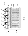
- a top view of a portion of a semiconductor die 900 that includes another embodiment of an impedance matching network 902 is illustrated.
- the impedance matching network 902 is one exemplary implementation of the impedance matching network 704 illustrated in FIG. 7 .
- the impedance matching network 902 is illustrated as formed in part on a semiconductor die 900 , upon which the various components have been formed or attached.
- the semiconductor die also may include a transistor 910 to which the impedance matching network 902 is electrically coupled.
- the transistor 910 includes a gate (implemented in part with gate contact fingers 912 ), a source region (not shown), and a drain region (not shown) to which drain contact fingers 914 are coupled. Although transistor 910 is shown unobscured in FIG. 9 , an arbitrary number of alternating conductive (or metallization) layers and dielectric layers are formed (or built up) overlying the transistor 910 , with the lowest metallization layer closest to the substrate, and the highest metallization layer farthest from the substrate.
- the impedance matching network 902 includes a bond pad capacitor 940 implemented at least in part with a first capacitor plate 942 , a second capacitor plate 944 , and dielectric material between the capacitor plates 942 , 944 . Also included in the impedance matching network 902 are inductances implemented with bond wires 920 and integrated inductors 922 .
- capacitor plates 942 and 944 are example structures that show how capacitor 706 ( FIG. 7 ) could be implemented.
- bond wires 920 are examples of how inductance 720 ( FIG. 7 ) could be implemented, and integrated inductors 922 are examples of how inductances 722 ( FIG. 7 ) could be implemented.
- the first capacitor plate 942 and the second capacitor plate 944 are formed in corresponding metallization layers formed on a semiconductor wafer.
- the second capacitor plate 944 is formed from a portion of the highest metallization layer, and openings are formed through the second capacitor plate 944 and the underlying dielectric material, and these openings allow the bond wires 920 to pass through and be physically connected to the underlying capacitor plate 942 .
- a first capacitor plate 942 which includes multiple bond pads, is coupled to the amplifier output (e.g., transistor 910 drain fingers 914 ) through feeds 916 within the build-up structure.
- the second capacitor plate 944 is coupled to the ground reference (e.g., ground reference 718 ) through the integrated inductors 922 .
- the integrated inductors 922 may be formed within one or more of the metallization layers overlying the semiconductor substrate, where first ends of the inductors 922 are coupled to the second capacitor plate 944 , and second ends of the inductors 922 are coupled with through substrate vias to a ground reference plane on the bottom of the semiconductor substrate.
- the impedance matching network that includes a bond pad capacitor can be implemented as an output impedance matching network coupled to an amplifier output. Examples of such embodiments were illustrated in FIGS. 2-4 and 7 .
- the impedance matching network can be implemented as an input impedance matching network coupled to an amplifier input (e.g., to a gate terminal of the amplifier transistor).
- a bond pad capacitor can be implemented as part of an input impedance matching network.
- the amplifier device 1000 includes a transistor 1002 , an input impedance matching network 1004 , and an output impedance matching network 1050 .
- the output impedance matching network 1050 can comprise any of the various embodiments described above, or any other suitable output impedance matching network.
- the input impedance matching network 1004 includes a bond pad capacitor 1006 , and series and shunt inductances 1020 and 1022 .
- the bond pad capacitor 1006 is coupled between the RF signal source 1012 and the transistor 1002 input (e.g., gate terminal).
- the series inductance 1020 is coupled between the RF signal source 1012 and a first plate of the bond pad capacitor 1006 .
- a second plate of the bond pad capacitor 1006 is coupled to the gate of the transistor 1002 .
- the shunt inductance 1022 is coupled between the first plate of the bond pad capacitor 1006 and a ground reference 1018 . Together, these elements implement the input impedance matching network 1004 .
- an additional inductance 1026 is coupled between a DC bias source and the transistor 1002 input.
- the bond pad capacitor 1006 is implemented to be in series with the transistor 1002 input.
- the bond pad capacitor 1006 of the input impedance matching network 1004 could be implemented in shunt between the transistor 1002 input and the ground reference 1018 , similar to the output impedance matching network illustrated in FIG. 7 .
- the bond pad capacitor 1006 can be implemented with various metallization layers on a semiconductor die using to form one or more capacitor plates.
- the inductances 1020 , 1022 and 1026 can be implemented with various structures, including bonding wires, integrated passive devices (IPD) and discrete inductors.
- an amplifier device comprising: an amplifier formed on a semiconductor die, the amplifier including an amplifier input and an amplifier output, the amplifier configured to generate an amplified radio frequency (RF) signal at the amplifier output; and an impedance matching network coupled to the amplifier, the impedance matching network including a capacitor, where the capacitor includes a first plate, a second plate, and dielectric material between the first and second plates, where the first plate includes or is directly electrically coupled to a bond pad on the semiconductor die.
- RF radio frequency
- an amplifier device comprising: a device package including at least one output lead and at least one input lead, the device package encasing at least one semiconductor die; an amplifier formed on the semiconductor die, the amplifier including an amplifier input and an amplifier output, the amplifier configured to generate an amplified radio frequency (RF) signal at the amplifier output; and a bond pad formed on the semiconductor die, the bond pad coupled to the amplifier, and the bond pad forming at least part of a capacitor, where the capacitor is part of an impedance matching network for the amplifier; and bonding wires physically connected to the bond pad.
- RF radio frequency
- node means any internal or external reference point, connection point, junction, signal line, conductive element, or the like, at which a given signal, logic level, voltage, data pattern, current, or quantity is present.
- two or more nodes may be realized by one physical element (and two or more signals can be multiplexed, modulated, or otherwise distinguished even though received or output at a common node).
Abstract
Description
Claims (26)
Priority Applications (1)
| Application Number | Priority Date | Filing Date | Title |
|---|---|---|---|
| US15/187,376 US9800213B1 (en) | 2016-06-20 | 2016-06-20 | Amplifier devices with impedance matching networks that incorporate a capacitor integrated with a bond pad |
Applications Claiming Priority (1)
| Application Number | Priority Date | Filing Date | Title |
|---|---|---|---|
| US15/187,376 US9800213B1 (en) | 2016-06-20 | 2016-06-20 | Amplifier devices with impedance matching networks that incorporate a capacitor integrated with a bond pad |
Publications (1)
| Publication Number | Publication Date |
|---|---|
| US9800213B1 true US9800213B1 (en) | 2017-10-24 |
Family
ID=60082278
Family Applications (1)
| Application Number | Title | Priority Date | Filing Date |
|---|---|---|---|
| US15/187,376 Active US9800213B1 (en) | 2016-06-20 | 2016-06-20 | Amplifier devices with impedance matching networks that incorporate a capacitor integrated with a bond pad |
Country Status (1)
| Country | Link |
|---|---|
| US (1) | US9800213B1 (en) |
Cited By (5)
| Publication number | Priority date | Publication date | Assignee | Title |
|---|---|---|---|---|
| US20150243649A1 (en) * | 2014-02-21 | 2015-08-27 | Infineon Technologies Ag | Power Transistor Die with Capacitively Coupled Bond Pad |
| EP3561869A1 (en) * | 2018-04-23 | 2019-10-30 | NXP USA, Inc. | Impedance matching circuit for rf devices and method therefor |
| EP3627551A1 (en) * | 2018-09-24 | 2020-03-25 | NXP USA, Inc. | Feed structure, electrical component including the feed structure, and module |
| CN112821907A (en) * | 2020-12-31 | 2021-05-18 | 锐石创芯(深圳)科技有限公司 | Input impedance matching network and radio frequency front end module |
| US11133275B2 (en) * | 2016-09-30 | 2021-09-28 | Semiconductor Manufacturing International (Beijing) Corporation | Method for improving wire bonding strength of an image sensor |
Citations (5)
| Publication number | Priority date | Publication date | Assignee | Title |
|---|---|---|---|---|
| US20060038632A1 (en) | 2004-08-20 | 2006-02-23 | Dow-Chih Niu | Series-parallel resonant matching circuit and broadband amplifier thereof |
| US7190083B1 (en) * | 2002-01-07 | 2007-03-13 | Vixs Systems, Inc. | High frequency integrated circuit using capacitive bonding |
| US7564303B2 (en) | 2005-07-26 | 2009-07-21 | Infineon Technologies Ag | Semiconductor power device and RF signal amplifier |
| US8717102B2 (en) | 2011-09-27 | 2014-05-06 | Infineon Technologies Ag | RF device with compensatory resonator matching topology |
| US20150295547A1 (en) | 2012-10-31 | 2015-10-15 | Freescale Semiconductor, Inc. | Amplification stage and wideband power amplifier |
-
2016
- 2016-06-20 US US15/187,376 patent/US9800213B1/en active Active
Patent Citations (5)
| Publication number | Priority date | Publication date | Assignee | Title |
|---|---|---|---|---|
| US7190083B1 (en) * | 2002-01-07 | 2007-03-13 | Vixs Systems, Inc. | High frequency integrated circuit using capacitive bonding |
| US20060038632A1 (en) | 2004-08-20 | 2006-02-23 | Dow-Chih Niu | Series-parallel resonant matching circuit and broadband amplifier thereof |
| US7564303B2 (en) | 2005-07-26 | 2009-07-21 | Infineon Technologies Ag | Semiconductor power device and RF signal amplifier |
| US8717102B2 (en) | 2011-09-27 | 2014-05-06 | Infineon Technologies Ag | RF device with compensatory resonator matching topology |
| US20150295547A1 (en) | 2012-10-31 | 2015-10-15 | Freescale Semiconductor, Inc. | Amplification stage and wideband power amplifier |
Cited By (10)
| Publication number | Priority date | Publication date | Assignee | Title |
|---|---|---|---|---|
| US20150243649A1 (en) * | 2014-02-21 | 2015-08-27 | Infineon Technologies Ag | Power Transistor Die with Capacitively Coupled Bond Pad |
| US11133275B2 (en) * | 2016-09-30 | 2021-09-28 | Semiconductor Manufacturing International (Beijing) Corporation | Method for improving wire bonding strength of an image sensor |
| EP3561869A1 (en) * | 2018-04-23 | 2019-10-30 | NXP USA, Inc. | Impedance matching circuit for rf devices and method therefor |
| US10707180B2 (en) | 2018-04-23 | 2020-07-07 | Nxp Usa, Inc. | Impedance matching circuit for RF devices and method therefor |
| EP3627551A1 (en) * | 2018-09-24 | 2020-03-25 | NXP USA, Inc. | Feed structure, electrical component including the feed structure, and module |
| CN110943281A (en) * | 2018-09-24 | 2020-03-31 | 恩智浦美国有限公司 | Feeding structure, electric component including feeding structure, and module |
| US10615510B1 (en) | 2018-09-24 | 2020-04-07 | Nxp Usa, Inc. | Feed structure, electrical component including the feed structure, and module |
| CN110943281B (en) * | 2018-09-24 | 2024-03-12 | 恩智浦美国有限公司 | Feeding structure, electrical component comprising a feeding structure, and module |
| CN112821907A (en) * | 2020-12-31 | 2021-05-18 | 锐石创芯(深圳)科技有限公司 | Input impedance matching network and radio frequency front end module |
| CN112821907B (en) * | 2020-12-31 | 2022-06-21 | 锐石创芯(深圳)科技股份有限公司 | Input impedance matching network and radio frequency front end module |
Similar Documents
| Publication | Publication Date | Title |
|---|---|---|
| US10630246B2 (en) | Methods of manufacturing encapsulated semiconductor device package with heatsink opening | |
| US10637400B2 (en) | RF amplifier with conductor-less region underlying filter circuit inductor, and methods of manufacture thereof | |
| EP3331161B1 (en) | Amplifier die with elongated side pads, and amplifier modules that incorporate such amplifier die | |
| US9800213B1 (en) | Amplifier devices with impedance matching networks that incorporate a capacitor integrated with a bond pad | |
| US9979361B1 (en) | Input circuits for RF amplifier devices, and methods of manufacture thereof | |
| US9571044B1 (en) | RF power transistors with impedance matching circuits, and methods of manufacture thereof | |
| US9799627B2 (en) | Semiconductor package structure and method | |
| EP3337037A1 (en) | Doherty amplifiers and amplifier modules with shunt inductance circuits that affect transmission line length between carrier and peaking amplifier outputs | |
| US9438184B2 (en) | Integrated passive device assemblies for RF amplifiers, and methods of manufacture thereof | |
| EP3247038A1 (en) | Multiple-path rf amplifiers with angularly offset signal path directions, and methods of manufacture thereof | |
| CN109818581B (en) | Multi-path amplifier with series components of inverters along output terminals of the amplifier | |
| US10742178B2 (en) | Broadband power transistor devices and amplifiers and methods of manufacture thereof | |
| US10381984B2 (en) | Amplifiers and amplifier modules with shunt inductance circuits that include high-Q capacitors | |
| CN107070419B (en) | Output impedance matching circuit for RF amplifier device and method of manufacturing the same | |
| TWI798670B (en) | Stacked rf circuit topology | |
| KR20190125942A (en) | Amplifiers and amplifier modules with ground plane height variation structures | |
| US11088661B2 (en) | Power amplifier devices containing inverted power transistor dies and methods for the fabrication thereof | |
| US11349438B2 (en) | Power amplifier packages containing multi-path integrated passive devices | |
| US20200059204A1 (en) | Amplifiers with broadband impedance matching and methods of manufacture thereof | |
| US20210050820A1 (en) | Integrated multiple-path power amplifier with interdigitated transistors | |
| US10784821B2 (en) | High power radio frequency amplifiers and methods of manufacture thereof | |
| US20230260935A1 (en) | Transistor with integrated passive components | |
| EP4343837A1 (en) | Power amplifier device having dies with elongated bondpads connected through a device substrate |
Legal Events
| Date | Code | Title | Description |
|---|---|---|---|
| AS | Assignment |
Owner name: FREESCALE SEMICONDUCTOR INC., TEXAS Free format text: ASSIGNMENT OF ASSIGNORS INTEREST;ASSIGNORS:KHALIL, IBRAHIM;SERAGI, EBRAHIM AL;JONES, JEFFREY K.;REEL/FRAME:039092/0280 Effective date: 20160617 |
|
| AS | Assignment |
Owner name: NXP USA, INC., TEXAS Free format text: CORRECTIVE ASSIGNMENT TO CORRECT THE CONVEYING PARTY DATA AND ASSIGNMENT DOCUMENT PREVIOUSLY RECORDED AT REEL: 039092 FRAME: 0280. ASSIGNOR(S) HEREBY CONFIRMS THE ASSIGNMENT;ASSIGNORS:KHALIL, IBRAHIM;AL SERAGI, EBRAHIM M.;JONES, JEFFREY K.;SIGNING DATES FROM 20160617 TO 20160908;REEL/FRAME:041479/0730 |
|
| AS | Assignment |
Owner name: NXP USA, INC., TEXAS Free format text: CHANGE OF NAME;ASSIGNOR:FREESCALE SEMICONDUCTOR INC.;REEL/FRAME:040626/0683 Effective date: 20161107 |
|
| AS | Assignment |
Owner name: NXP USA, INC., TEXAS Free format text: CORRECTIVE ASSIGNMENT TO CORRECT THE NATURE OF CONVEYANCE PREVIOUSLY RECORDED AT REEL: 040626 FRAME: 0683. ASSIGNOR(S) HEREBY CONFIRMS THE MERGER AND CHANGE OF NAME EFFECTIVE NOVEMBER 7, 2016;ASSIGNORS:NXP SEMICONDUCTORS USA, INC. (MERGED INTO);FREESCALE SEMICONDUCTOR, INC. (UNDER);SIGNING DATES FROM 20161104 TO 20161107;REEL/FRAME:041414/0883 |
|
| STCF | Information on status: patent grant |
Free format text: PATENTED CASE |
|
| MAFP | Maintenance fee payment |
Free format text: PAYMENT OF MAINTENANCE FEE, 4TH YEAR, LARGE ENTITY (ORIGINAL EVENT CODE: M1551); ENTITY STATUS OF PATENT OWNER: LARGE ENTITY Year of fee payment: 4 |