US9799385B2 - Resistance change memory - Google Patents
Resistance change memory Download PDFInfo
- Publication number
- US9799385B2 US9799385B2 US14/644,148 US201514644148A US9799385B2 US 9799385 B2 US9799385 B2 US 9799385B2 US 201514644148 A US201514644148 A US 201514644148A US 9799385 B2 US9799385 B2 US 9799385B2
- Authority
- US
- United States
- Prior art keywords
- transistor
- circuit
- current
- resistance change
- voltage
- Prior art date
- Legal status (The legal status is an assumption and is not a legal conclusion. Google has not performed a legal analysis and makes no representation as to the accuracy of the status listed.)
- Active
Links
Images


Classifications
-
- G—PHYSICS
- G11—INFORMATION STORAGE
- G11C—STATIC STORES
- G11C11/00—Digital stores characterised by the use of particular electric or magnetic storage elements; Storage elements therefor
- G11C11/02—Digital stores characterised by the use of particular electric or magnetic storage elements; Storage elements therefor using magnetic elements
- G11C11/16—Digital stores characterised by the use of particular electric or magnetic storage elements; Storage elements therefor using magnetic elements using elements in which the storage effect is based on magnetic spin effect
- G11C11/165—Auxiliary circuits
- G11C11/1673—Reading or sensing circuits or methods
-
- G—PHYSICS
- G11—INFORMATION STORAGE
- G11C—STATIC STORES
- G11C13/00—Digital stores characterised by the use of storage elements not covered by groups G11C11/00, G11C23/00, or G11C25/00
- G11C13/0002—Digital stores characterised by the use of storage elements not covered by groups G11C11/00, G11C23/00, or G11C25/00 using resistive RAM [RRAM] elements
- G11C13/0021—Auxiliary circuits
- G11C13/004—Reading or sensing circuits or methods
-
- G—PHYSICS
- G11—INFORMATION STORAGE
- G11C—STATIC STORES
- G11C7/00—Arrangements for writing information into, or reading information out from, a digital store
- G11C7/04—Arrangements for writing information into, or reading information out from, a digital store with means for avoiding disturbances due to temperature effects
-
- G—PHYSICS
- G11—INFORMATION STORAGE
- G11C—STATIC STORES
- G11C13/00—Digital stores characterised by the use of storage elements not covered by groups G11C11/00, G11C23/00, or G11C25/00
- G11C13/0002—Digital stores characterised by the use of storage elements not covered by groups G11C11/00, G11C23/00, or G11C25/00 using resistive RAM [RRAM] elements
- G11C13/0021—Auxiliary circuits
- G11C13/004—Reading or sensing circuits or methods
- G11C2013/0042—Read using differential sensing, e.g. bit line [BL] and bit line bar [BLB]
-
- G—PHYSICS
- G11—INFORMATION STORAGE
- G11C—STATIC STORES
- G11C13/00—Digital stores characterised by the use of storage elements not covered by groups G11C11/00, G11C23/00, or G11C25/00
- G11C13/0002—Digital stores characterised by the use of storage elements not covered by groups G11C11/00, G11C23/00, or G11C25/00 using resistive RAM [RRAM] elements
- G11C13/0021—Auxiliary circuits
- G11C13/004—Reading or sensing circuits or methods
- G11C2013/0054—Read is performed on a reference element, e.g. cell, and the reference sensed value is used to compare the sensed value of the selected cell
Definitions
- Embodiments described herein relate generally to a resistance change memory that stores data by using the change of the resistance value of a memory element.
- a nonvolatile memory such as a resistance change memory (e.g., a magnetoresistive random access memory: MRAM, a phase change random access memory: PRAM, or a resistive random access memory: ReRAM).
- MRAM magnetoresistive random access memory
- PRAM phase change random access memory
- ReRAM resistive random access memory
- the change of its resistance value caused by the application of a current (or voltage) is used to determine whether data is “1” or “0”.
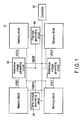
- FIG. 1 is a block diagram showing the schematic configuration of an MRAM according to an embodiment
- FIG. 2 is a circuit diagram showing the configuration of a memory block according to the embodiment
- FIG. 3 is a sectional view of an MTJ element according to the embodiment.
- FIG. 4 is a circuit diagram showing the configurations of a sense amplifier and a reference voltage generating circuit according to a first embodiment
- FIG. 5 is a graph showing the temperature characteristics of a current IBGR according to the first embodiment
- FIG. 6 is a graph showing the temperature characteristics of a reference resistance Rref according to the first embodiment
- FIG. 7 is a circuit diagram of a potential generating circuit in a reference voltage generating circuit 30 according to the first embodiment
- FIG. 8 is a graph showing the temperature characteristics of currents I 1 and I 2 in the potential generating circuit
- FIG. 9 is a graph showing the temperature characteristics of the current IBGR in the potential generating circuit.
- FIG. 10 is a flowchart showing a process of determining a clamp voltage and a reference voltage
- FIG. 11 is a graph showing the relation between the clamp voltage and a reference current as well as a cell current
- FIG. 12 is a circuit diagram showing the configurations of a sense amplifier and a reference voltage generating circuit according to a second embodiment
- FIG. 13 is a graph showing the temperature characteristics of a voltage Vx according to the second embodiment
- FIG. 14 is a graph showing the temperature characteristics of a reference resistance Rref according to the second embodiment.
- FIG. 15 is a circuit diagram of a potential generating circuit according to a modification.
- a resistance change memory includes a memory cell, a reference voltage generating circuit, a first transistor and a sense amplifier.
- the memory cell includes a resistance change element.
- the reference voltage generating circuit generates a reference adjustment voltage.
- the first transistor provides a reference current in accordance with the reference adjustment voltage.
- the sense amplifier compares a cell current flowing through the memory cell with the reference current flowing through the first transistor.
- an MRAM is described as an example of the resistance change memory.
- a three-terminal device such as an n-channel MOS transistor (hereinafter, a reference transistor) is used for a reference current Iref to provide a reference resistance.
- a reference voltage having temperature characteristics is supplied to the gate of the reference transistor to allow the reference transistor to serve as a reference resistance having temperature characteristics.
- FIG. 1 is a block diagram showing the schematic configuration of the MRAM according to the first embodiment.
- the MRAM comprises a memory block 10 , a clamp voltage generating circuit 20 , a reference voltage generating circuit 30 , a potential generating circuit 40 , and a controller 50 .
- the memory block 10 has, for example, a memory cell array, a sense amplifier (S/A), and a row decoder.
- the memory cell array includes memory cells.
- the clamp voltage generating circuit 20 generates a clamp voltage Vclamp to restrict a cell current flowing through the memory cells.
- the reference voltage generating circuit 30 generates a reference voltage VREF to control a reference current.
- the potential generating circuit 40 generates a voltage VBGR.
- the controller 50 performs overall control of the operations of the memory block 10 , the clamp voltage generating circuit 20 , the reference voltage generating circuit 30 , and the potential generating circuit 40 .
- the controller 50 receives an address (including a row address and a column address), and control signals such as a clock signal and a command.
- the controller 50 supplies various control signals and various voltages to the memory block 10 , the clamp voltage generating circuit 20 , the reference voltage generating circuit 30 , and the potential generating circuit 40 to control the operations of these circuits.
- FIG. 2 is a circuit diagram showing the configuration of the memory block according to the first embodiment.
- the memory block 10 comprises a memory cell array 11 , a sense amplifier 12 , and a row decoder 13 .
- memory cells MC there are arranged memory cells MC, bit lines BL ⁇ 0>, BL ⁇ 1>, . . . , and BL ⁇ n>, source lines SL ⁇ 0>, SL ⁇ 1>, . . . , and SL ⁇ n>, word lines WL ⁇ 0>, WL ⁇ 1>, . . . , and WL ⁇ m>, and reference bit lines RefL ⁇ 0>, RefL ⁇ 1>, . . . , and RefL ⁇ n>.
- n and m are natural numbers equal to or more than 0.
- the memory cells MC are arrayed in a matrix form.
- the memory cell MC is coupled between the bit line BL and the source line SL.
- the memory cell MC comprises a magnetoresistive effect element such as a magnetic tunnel junction (MTJ) element RE to serve as a resistance change element, and a select transistor ST.
- the select transistor ST comprises, for example, an n-channel MOS field effect transistor (hereinafter, an nMOS transistor).
- an nMOS transistor n-channel MOS field effect transistor
- the word line WL is disposed to intersect (e.g., intersect at right angles) with the bit line BL and the source line SL. One end of the word line WL is coupled to the row decoder 13 .
- One row of the memory cell array, that is, one page of memory cells is coupled to one word line WL, and one column of the memory cell array is coupled to a pair including one bit line BL and one source line SL.
- the drain of the select transistor ST is coupled to the bit line BL, and the source of the select transistor ST is coupled to one end of the MTJ element RE.
- the other end of the MTJ element RE is coupled to the source line SL.
- the gate of the select transistor ST is coupled to the word line WL.
- the bit line BL is coupled to a first input terminal (+) of the sense amplifier 12 via a clamp transistor T 11 .
- the source line SL is coupled to a reference voltage such as a ground voltage GND.
- One end of the reference bit line RefL is coupled to a second input terminal ( ⁇ ) of the sense amplifier 12 via an nMOS transistor T 12 .
- the other end of the reference bit line RefL is coupled to the reference voltage via a reference transistor Tref. That is, the second input terminal of the sense amplifier 12 is coupled to the reference voltage via the nMOS transistor T 12 and the reference transistor Tref that are coupled in series.
- the clamp transistor T 11 and the reference transistor Tref each comprises, for example, an nMOS transistor.
- the clamp voltage generating circuit 20 supplies the clamp voltage Vclamp to the gates of the clamp transistor T 11 and the nMOS transistor T 12 . Because of this clamp voltage Vclamp, the clamp transistor T 11 restricts the cell current to prevent read disturb in the memory cell MC.
- the reference voltage generating circuit 30 supplies the reference voltage VREF to the gate of the reference transistor Tref.
- the reference transistor Tref changes in resistance value in response to the temperature of the place where the memory cell MC is placed, that is, the temperature of the memory cell. That is, the reference transistor Tref acts as a reference resistance Rref having temperature characteristics corresponding to the temperature characteristics of the memory cell MC.
- the reference transistor Tref acts as the reference resistance Rref having a temperature dependence equivalent to the temperature dependence of the resistance value of the memory cells MC due to the control of the reference voltage VREF.
- the row decoder 13 selects one of the word lines WL ⁇ 0> to WL ⁇ m> in accordance with the row address.
- the sense amplifier 12 reads data stored in the memory cells MC.
- the sense amplifier 12 of, for example, a current detection type, compares a cell current ICELL flowing through the memory cell MC via the bit line BL with the reference current Iref flowing through the reference transistor Tref via the reference bit line RefL, and thereby reads the data stored in the selected memory cell, that is, detects and amplifies the data stored in the selected memory cell.
- the sense amplifier 12 outputs the data read from the selected memory cell as output signals Out ⁇ 0>, Out ⁇ 1>, . . . , and Out ⁇ n> from output terminals, respectively.
- FIG. 3 is a sectional view of the MTJ element RE.
- the MTJ element RE comprises a lower electrode 100 , a storage layer (also referred to as a free layer) 101 , a nonmagnetic layer (tunnel barrier layer) 102 , a reference layer (also referred to as a fixed layer) 103 , and an upper electrode 104 that are stacked in order.
- the storage layer 101 and the reference layer 103 may be stacked in reverse order.
- the storage layer 101 and the reference layer 103 are each made of a ferromagnetic material.
- An insulating material such as MgO is used as the tunnel barrier layer 102 .
- the storage layer 101 and the reference layer 103 each have perpendicular magnetic anisotropy, and their easy magnetization directions are perpendicular directions.
- the magnetization directions of the storage layer 101 and the reference layer 103 may be in-plane directions.
- the magnetization direction of the storage layer 101 is variable (inverted).
- the magnetization direction of the reference layer 103 is invariable (fixed).
- the reference layer 103 is set to have sufficiently higher perpendicular magnetic anisotropic energy than the storage layer 101 .
- the magnetic anisotropy can be set by adjusting the material constitution and thickness.
- a magnetization inversion current for the storage layer 101 is lower, and a magnetization inversion current for the reference layer 103 is higher than that for the storage layer 101 .
- a spin-transfer torque writing method is used so that a write current is directly passed through the MTJ element RE, and the magnetization state of the MTJ element RE is controlled by this write current.
- the MTJ element RE can take one of a low-resistance state and a high-resistance state depending on whether the magnetizations of the storage layer 101 and the reference layer 103 are parallel or antiparallel.
- the low-resistance state of the MTJ element RE is defined as, for example, data “0”.
- the magnetizations of the storage layer 101 and the reference layer 103 are antiparallel.
- the resistance value of the MTJ element RE is highest, and the MTJ element RE is set to the high-resistance state.
- the high-resistance state of the MTJ element RE is defined as, for example, data “1”.
- the MTJ element RE can be used as a storage element capable of storing one-bit data (binary data). Any resistance state of the MTJ element RE and any allocation of data can be set.
- a read voltage is applied to the MTJ element RE, and the resistance value of the MTJ element RE is detected in accordance with a read current flowing through the MTJ element RE at the moment.
- This read voltage is set to a value sufficiently lower than a threshold at which the magnetization is reversed by spin-transfer torque.
- FIG. 4 is a circuit diagram showing the configurations of the sense amplifier 12 and the reference voltage generating circuit 30 according to the first embodiment.
- one end of a cell resistance Rcell is coupled to the first input terminal (+) of the sense amplifier 12 via the clamp transistor T 11 .
- the other end of the cell resistance Rcell is coupled to the reference voltage.
- the cell resistance Rcell indicates the resistance of the memory cell MC.
- the first input terminal of the sense amplifier 12 is coupled to the reference voltage via the bit line BL, the memory cell MC, and the source line SL.
- One end of the current path of the reference transistor Tref is coupled to the second input terminal ( ⁇ ) of the sense amplifier 12 via the nMOS transistor T 12 .
- the other end of the current path of the reference transistor Tref is coupled to the reference voltage.
- the clamp voltage Vclamp is supplied to the gates of the clamp transistor T 11 and the nMOS transistor T 12 .
- the reference voltage generating circuit 30 has the following configuration.
- the reference voltage generating circuit 30 has a p-channel MOS field effect transistor (hereinafter, a pMOS transistor) T 13 , a replica transistor T 14 , an operational amplifier OP 1 , and a resistance dividing circuit 60 .
- the replica transistor T 14 comprises an n-channel MOS transistor.
- the source of the pMOS transistor T 13 is coupled to a power supply voltage VDD, and the drain of the pMOS transistor T 13 is coupled to the drain of the replica transistor T 14 .
- the source of the replica transistor T 14 is coupled to the reference voltage. Further, the voltage VBGR is supplied to the gate of the pMOS transistor T 13 from the potential generating circuit 40 .
- a noninverting input terminal (+) of the operational amplifier OP 1 is coupled to the drain of the replica transistor T 14 .
- An inverting input terminal ( ⁇ ) of the operational amplifier OP 1 is coupled to the resistance dividing circuit 60 . That is, the inverting input terminal of the operational amplifier OP 1 is coupled between a resistance R 2 , resistances R 3 - 0 , . . . , and R 3 -X that are coupled in parallel, and a resistance R 1 .
- the inverting input terminal is coupled to one end of each of the resistance R 2 , the resistances R 3 - 0 , . . . , and R 3 -X, and the resistance R 1 .
- the other end of the resistance R 1 is coupled to the power supply voltage VDD.
- the other end of the resistance R 2 is coupled to the reference voltage, and the other ends of the resistances R 3 - 0 , . . . , and R 3 -X are coupled to the reference voltages via nMOS transistors T 15 - 0 , . . . , and T 15 -X, respectively. Further, test mode signals TM ⁇ 0>, . . . , and TM ⁇ X> are input to the gates of the nMOS transistors T 15 - 0 , . . . , and T 15 -X. X is a natural number equal to or more than 0.
- An output terminal of the operational amplifier OP 1 is coupled to the gate of the replica transistor T 14 and the gate of the reference transistor Tref.
- the common clamp voltage Vclamp is supplied to the gate of the clamp transistor T 11 and the gate of the nMOS transistor T 12 .
- the reference transistor Tref corresponds to the reference resistance Rref for generating the reference current Iref.
- the reference transistor Tref operates in a triode region (linear region) by the control of a gate potential.
- means for controlling the gate potential of the reference transistor Tref that is, the reference voltage generating circuit 30 is provided.
- the reference voltage generating circuit 30 comprises a negative feedback circuit including the replica transistor T 14 of the reference transistor Tref and the operational amplifier OP 1 which forms the drain potential of the replica transistor T 14 into a predetermined voltage Vx, and the pMOS transistor T 13 which supplies a current IBGR.
- the current IBGR is generated by a current mirror in the potential generating circuit 40 , and is set to have desired temperature characteristics.
- the resistance value of the replica transistor T 14 is Vx/IBGR. Therefore, if the voltage Vx is varied by the test mode signals TM ⁇ 0>, . . . , and TM ⁇ X> and if the temperature characteristics of the current IBGR are set to desired characteristics by the potential generating circuit 40 , it is possible to generate the reference voltage VREF which sets the resistance value of the replica transistor T 14 to a desired resistance value that follows the temperature characteristics and process conditions of the cell resistance Rcell.
- the clamp voltage Vclamp is adjusted to set the drain potential of the reference transistor Tref to the voltage Vx. If the reference voltage VREF is input to the gate of the reference transistor Tref, the resistance value (reference resistance Rref) of the reference transistor Tref will be Vx/Iref.
- FIGS. 5 and 6 are graphs showing the temperature characteristics of the current IBGR and the temperature characteristics of the reference resistance Rref, respectively.
- the reference resistance Rref has positive temperature characteristics, that is, when the current IBGR has such characteristics as to increase as the temperature rises (IA in FIG. 5 )
- the reference resistance Rref has negative temperature characteristics, that is, the reference resistance Rref has such characteristics as to decrease as the temperature rises (RA in FIG. 6 ).
- the reference resistance Rref has positive temperature characteristics, that is, the reference resistance Rref has such characteristics as to increase as the temperature rises (RB in FIG. 6 ).
- the reference resistance Rref does not have temperature characteristics either, that is, the reference resistance Rref does not change in spite of the temperature change (RC in FIG. 6 ).
- FIG. 7 shows one example of a circuit configuration for supplying the current IBGR in the reference voltage generating circuit 30 .
- the circuit for supplying the current IBGR includes a current generating unit A, a current generating unit B, and a current mirror unit C.
- the current generating unit A has diodes D 1 and D 2 , a resistance R 3 , an operational amplifier OP 2 , and pMOS transistors T 21 and T 22 , and generates a current I 1 having positive temperature characteristics.
- the positive temperature characteristics are such characteristics that the current I 1 increases as a temperature rises.
- the current generating unit B has a diode D 3 , a resistance R 4 , an operational amplifier OP 3 , and pMOS transistors T 23 and T 24 , and generates a current I 2 having negative temperature characteristics.
- the negative temperature characteristics are such characteristics that the current I 2 decreases as the temperature rises.
- the current mirror unit C includes nMOS transistors T 25 and T 26 , a pMOS transistor T 27 , and circuit units W 1 and W 2 .
- the circuit unit W 1 includes a pMOS transistor T 31 coupled between the drain of the nMOS transistor T 25 and the power supply voltage VDD.
- the circuit unit W 1 further includes pMOS transistors T 32 - 0 and T 33 - 0 , pMOS transistors T 32 - 1 , T 33 - 1 , and . . . , and pMOS transistors T 32 - g and T 33 - g that are coupled in series between the drain of the nMOS transistor T 25 and the power supply voltage VDD.
- a voltage output from the output terminal of the operational amplifier OP 2 is supplied to the gates of the pMOS transistors T 32 - 0 , T 32 - 1 , . . .
- Test mode signals bTM 1 ⁇ 0>, bTM 1 ⁇ 1>, . . . , and bTM 1 ⁇ g > are supplied to the gates of the pMOS transistors T 33 - 0 , T 33 - 1 , . . . , and T 33 - g , respectively.
- g is a natural number equal to or more than 0.
- the circuit unit W 2 includes a pMOS transistor T 34 coupled between the drain of the nMOS transistor T 25 and the power supply voltage VDD.
- the circuit unit W 2 further includes pMOS transistors T 35 - 0 and T 36 - 0 , pMOS transistors T 35 - 1 and T 36 - 1 , . . . , and pMOS transistors T 35 - h and T 36 - h that are coupled in series between the drain of the nMOS transistor T 25 and the power supply voltage VDD.
- a voltage output from the output terminal of the operational amplifier OP 3 is supplied to the gates of the pMOS transistors T 35 - 0 , T 35 - 1 , . . .
- Test mode signals bTM 2 ⁇ 0>, bTM 2 ⁇ 1>, . . . , and bTM 2 ⁇ h> are supplied to the gates of the pMOS transistors T 36 - 0 , T 36 - 1 , . . . , and T 36 - h , respectively.
- h is a natural number equal to or more than 0.
- W 1 and W 2 represent coefficients weighted by the circuit units W 1 and W 2 .
- the coefficients W 1 and W 2 can be changed if the current mirror ratio is changed by the test mode signals bTM 1 and bTM 2 .
- FIG. 8 is a graph showing the temperature characteristics of the currents I 1 and I 2 in the potential generating circuit.
- FIG. 9 is a graph showing the temperature characteristics of the current IBGR in the potential generating circuit.
- the current generating unit A generates the current I 1 having the positive temperature characteristics. That is, the current generating unit A increases the current I 1 as a temperature rises as shown in FIG. 8 .
- the current generating unit B generates the current I 2 having the negative temperature characteristics. That is, the current generating unit B decreases the current I 2 as the temperature rises.
- the current mirror ratio is adjusted by the test mode signals bTM 1 and bTM 2 so that W 1 >W 2 .
- the current mirror ratio is adjusted by the test mode signals bTM 1 and bTM 2 so that W 1 ⁇ W 2 .
- “Low(L)” or “High(H)” is applied to the gates of the pMOS transistors T 33 - 0 to T 33 - g and T 36 - 0 to T 36 - h by the test mode signals bTM 1 and bTM 2 , and the pMOS transistors T 33 - 0 to T 33 - g and T 36 - 0 to T 36 - h are switched on or off.
- the magnitudes of the coefficient W 1 and the coefficient W 2 are adjusted by the number of the on-state pMOS transistors T 33 in the circuit unit W 1 and the number of the on-state pMOS transistors T 36 in the circuit unit W 2 at the moment. If it is not necessary for the current IBGR to have temperature characteristics, the current mirror ratio has only to be adjusted by the test mode signals bTM 1 and bTM 2 so that the coefficient W 1 and the coefficient W 2 will be equal to each other.
- a process of determining the potentials of the clamp voltage Vclamp and the reference voltage VREF is described.
- a test mode is conducted to determine the potentials of the clamp voltage Vclamp and the reference voltage VREF, and a fuse corresponding to the determined test mode is blown.
- FIG. 10 is a flowchart showing the process of determining the potentials of the clamp voltage Vclamp and the reference voltage VREF.
- the clamp voltage Vclamp is determined to be a potential that does not cause read disturb in the memory cell MC (step S 1 ).
- the optimum reference voltage VREF is then determined by the following procedure when the clamp voltage Vclamp determined in step S 1 is supplied.
- a temperature A e.g., room temperature
- a reference voltage VREFA which is optimum at the temperature A is determined.
- the MRAM is then put in an environment at a temperature B (e.g., a high temperature) higher than the temperature A, and a reference voltage VREFB which is optimum at the temperature B is determined.
- a test mode signal TM in the reference voltage generating circuit 30 that satisfies the reference voltages VREFA and VREFB and the test mode signals bTM 1 and bTM 2 in the potential generating circuit 40 are then selected (step S 2 ).
- the potential of the voltage Vx, and the absolute value and temperature characteristics of the current IBGR are determined, and the reference resistance Rref is determined from the voltage Vx and the current IBGR.
- the reference voltage VREF is determined by blowing the fuse corresponding to the test mode signal.
- the controller 50 may supply the test mode signal at the time of power supply starting to determine the reference voltage VREF.
- the resistance of the “0” cell and the resistance of the “1” cell vary from each other even in the same chip, and a cell current IC 0 flowing through the “0” cell and a cell current Id 1 flowing through the “1” cell have distributions shown in FIG. 11 .
- an optimum reference current lade that ensures the maximum sense margin in the sense amplifier is located in the center of the area between the distribution of the cell current IC 0 and the distribution of the cell current Id 1 .
- the cell resistance also varies according to chips, and therefore, the average value of the cell current IC 0 and the cell current IC 1 also varies according to chips.
- the reference current lade that should be located in the center of the area between the distribution of the cell current IC 0 and the distribution of the cell current IC 1 also varies according to chips. Therefore, the reference resistance Rref needs to be adjusted so that the reference current IREF corresponds to the optimum reference current lade for each chip.
- the cell resistance and the reference resistance are made of different kinds of materials, thus the problem is that it is difficult to satisfy the above-mentioned requirements under all conditions: process variations, voltage, and temperature.
- a three-terminal device such as an n-channel MOS transistor (reference transistor) is used as the reference resistance so that the reference voltage to be supplied to the gate of the reference transistor has temperature characteristics.
- the reference transistor is set to operate in a linear region in accordance with the reference voltage supplied to the gate.
- the reference voltage generating circuit generates a reference voltage having positive or negative temperature characteristics depending on the temperature characteristics of the memory cell (MTJ element).
- the reference voltage generating circuit can also generate a reference voltage having no temperature characteristics.
- the optimum resistance value is a resistance value at which a reference current that maximizes the sense margin at the temperature of the moment can be set.
- the MOS transistor which operates in the linear region (triode region) is used for the reference resistance unit for generating the reference current, and the gate voltage of this MOS transistor is controlled to be a desired potential, so that it is possible to obtain a sense amplifier which is robust against, for example, power supply bounce noise and which can ensure a sufficient sense margin even under conditions including temperature variations and process variations.
- the voltage Vx has temperature characteristics
- the current IBGR is a constant current having no temperature characteristics, so that the reference voltage generating circuit generates the reference voltage VREF having temperature characteristics.
- the MRAM, the memory block, and the MTJ element according to the second embodiment are similar in configuration to those according to the first embodiment, and are therefore not described.
- FIG. 12 is a circuit diagram showing the configurations of a sense amplifier 12 and a reference voltage generating circuit 31 according to the second embodiment.
- one end of a cell resistance Rcell is coupled to a first input terminal (+) of the sense amplifier 12 via a clamp transistor T 11 .
- the other end of the cell resistance Rcell is coupled to a reference voltage.
- the cell resistance Rcell indicates the resistance of a memory cell MC.
- One end of the current path of a reference transistor Tref is coupled to a second input terminal ( ⁇ ) of the sense amplifier 12 via the nMOS transistor T 12 .
- the other end of the current path of the reference transistor Tref is coupled to the reference voltage.
- the clamp voltage Vclamp is supplied to the gates of the clamp transistor T 11 and the nMOS transistor T 12 .
- the reference voltage generating circuit 31 has the following configuration.
- the reference voltage generating circuit 31 has a pMOS transistor T 13 , a replica transistor T 14 , a pMOS transistor T 16 , an operational amplifier OP 1 , and a Vx generating circuit 70 .
- the source of the pMOS transistor T 13 is coupled to a power supply voltage VDD, and the drain of the pMOS transistor T 13 is coupled to the drain of the replica transistor T 14 .
- the source of the replica transistor T 14 is coupled to the reference voltage.
- the source of the pMOS transistor T 16 is coupled to the power supply voltage VDD, and the drain of the pMOS transistor T 16 is coupled to an inverting input terminal ( ⁇ ) of the operational amplifier OP 1 .
- a noninverting input terminal (+) of the operational amplifier OP 1 is coupled to the drain of the replica transistor T 14 .
- An inverting input terminal of the operational amplifier OP 1 is coupled to the Vx generating circuit 70 . That is, a resistance R 5 - 0 and an nMOS transistor T 17 - 0 , and . . . , a resistance R 5 - i and an nMOS transistor T 17 - i , a diode D 4 - 0 and an nMOS transistor T 18 - 0 , and . . .
- Test mode signals TM ⁇ 0>, . . . , and TM ⁇ i> are input to the gates of the nMOS transistors T 17 - 0 , . . . , and T 17 - i . Further, test mode signals TM ⁇ 0>, . . . , and TM ⁇ j > are input to the gates of the nMOS transistors T 18 - 0 , . . . , and T 18 - j . i and j are natural numbers equal to or more than 0.
- a voltage VBGR is supplied to the gates of the pMOS transistor T 13 and the pMOS transistor T 16 from the potential generating circuit 40 .
- An output terminal of the operational amplifier OP 1 is coupled to the gate of the replica transistor T 14 and the gate of the reference transistor Tref.
- the reference voltage VREF is supplied to the gate of the reference transistor Tref from the output terminal of the operational amplifier OP 1 .
- the common clamp voltage Vclamp is supplied to the gate of the clamp transistor T 11 and the gate of the nMOS transistor T 12 .
- the reference transistor Tref corresponds to a reference resistance Rref for generating a reference current Iref.
- the reference transistor Tref operates in a triode region (linear region) by the control of a gate potential.
- means for controlling the gate potential of the reference transistor Tref that is, the reference voltage generating circuit 31 is provided.
- the reference voltage generating circuit 31 comprises a negative feedback circuit including the replica transistor T 14 of the reference transistor Tref and the operational amplifier OP 1 which forms the drain potential of the replica transistor T 14 into a predetermined voltage Vx, the pMOS transistor T 13 and T 16 which supply the current IBGR, and the Vx generating circuit 70 .
- the current IBGR is generated by a current mirror in the potential generating circuit 40 , and is a constant current having no temperature characteristics.
- the Vx generating circuit 70 generates the voltage Vx having temperature characteristics.
- the Vx generating circuit 70 has resistances R 5 - 0 , R 5 - 1 , . . . , and R 5 - i which increase in resistance value as a temperature rises, and diodes D 4 - 0 , D 4 - 1 , . . . , and D 4 - j which decrease in resistance value as the temperature rises. “Low(L)” or “High(H)” is applied to the gates of the nMOS transistors T 17 - 0 , T 17 - 1 , . . . , and T 17 - i , and T 18 - 0 , T 18 - 1 , .
- the test mode signals TM ⁇ 0>, . . . , and TM ⁇ i>, and TM ⁇ 0>, . . . , and TM ⁇ j> to switch on or off the nMOS transistors T 17 - 0 , T 17 - 1 , . . . , and T 17 - i , and T 18 - 0 , T 18 - 1 , . . . , and T 18 - j .
- the resistances R 5 - 0 to R 5 - i and the diodes D 4 - 0 to D 4 - j that are coupled between the inverting input terminal of the operational amplifier OP 1 and the reference voltage are selected.
- the resistances R 5 - 0 to R 5 - i have positive temperature characteristics
- the diodes D 4 - 0 to D 4 - j have negative temperature characteristics, so that as shown in FIG. 13 , the voltage Vx can have positive temperature characteristics (VxA in FIG. 13 ), have negative temperature characteristics (VxB in FIG. 13 ), or have no temperature characteristics (VxC in FIG. 13 ).
- the resistance value of the replica transistor T 14 is Vx/IBGR. Therefore, if the voltage Vx is varied by the test mode signals TM ⁇ 0>, . . . , and TM ⁇ i>, and TM ⁇ 0>, . . . , and TM ⁇ j> to provide temperature characteristics and if the current IBGR is a constant current having no temperature characteristics, it is possible to generate the reference voltage VREF which sets the resistance value of the replica transistor T 14 to a desired resistance value that follows the temperature characteristics and process conditions of the cell resistance Rcell.
- the clamp voltage Vclamp is adjusted to set the drain potential of the reference transistor Tref to the voltage Vx. If the reference voltage VREF is input to the gate of the reference transistor Tref, the resistance value (reference resistance Rref) of the reference transistor Tref will be Vx/Iref.
- the reference resistance Rref having temperature characteristics can be produced by the use of the current IBGR having no temperature characteristics (temperature dependence) and the voltage Vx having temperature characteristics. If the voltage Vx is adjusted so that the temperature characteristics of the memory cell are equivalent to, that is, correspond to the temperature characteristics of the reference resistance Rref, the reference current Iref flowing through the reference resistance Rref can correspond to the optimum reference current Iade.
- the configuration and advantageous effects are similar to those according to the first embodiment in other respects.
- the circuit having temperature characteristics is constructed by the use of the resistive element and the diode element that are general components used in the MRAM (memory chip).
- the potential generating circuit 40 in the first embodiment ( FIG. 4 ) or the second embodiment ( FIG. 12 ) can be constructed by the use of the above-mentioned MTJ element RE.
- FIG. 15 An example of the use of the MTJ element RE for the current generating unit in the potential generating circuit 40 is shown in FIG. 15 .
- the current generating units A and B shown in FIG. 4 are replaced with current generating units D and E.
- the current generating unit D has an MTJ element unit 41 , a pMOS transistor T 21 , and an nMOS transistor T 41 .
- the MTJ element unit 41 includes MTJ elements (e.g., N MTJ elements, N is a natural number equal to or more than 1). The magnetization of each of these MTJ elements is set to the parallel state.
- the current generating unit E has an MTJ element unit 42 , a pMOS transistor T 23 , and an nMOS transistor T 42 .
- the MTJ element unit 42 includes MTJ elements (e.g., N MTJ elements). The magnetization of each of these MTJ elements is set to the antiparallel state.
- a current sum of a current Ip of the MTJ element unit (the N parallel MTJ elements) 41 and a current Iap of the MTJ element unit (the N antiparallel MTJ elements) 42 is taken and averaged to produce an intermediate current between a current flowing through the memory cells having the parallel MTJ elements (hereinafter, P cells) and a current flowing through the memory cells having the antiparallel MTJ elements (hereinafter, AP cells).
- P cells a current flowing through the memory cells having the parallel MTJ elements
- AP cells a current flowing through the memory cells having the antiparallel MTJ elements
- the MTJ element itself is used, so that the intermediate current between the current Ip of the P cells and the current Iap of the AP cells can be always produced even if the temperature changes. Therefore, this example is suited to another circuit example of the potential generating circuit 40 .
- the present invention is not limited thereto.
- the present invention is also applicable to various kinds of semiconductor storage devices including volatile memories and nonvolatile memories.
- the present invention is also applicable to a resistance change memory of the same kind as the MRAM such as a resistive random access memory (ReRAM) or a phase-change random access memory (PCRAM).
- ReRAM resistive random access memory
- PCRAM phase-change random access memory
Landscapes
- Engineering & Computer Science (AREA)
- Computer Hardware Design (AREA)
- Mram Or Spin Memory Techniques (AREA)
Abstract
Description
Claims (16)
Priority Applications (2)
| Application Number | Priority Date | Filing Date | Title |
|---|---|---|---|
| US14/644,148 US9799385B2 (en) | 2014-09-08 | 2015-03-10 | Resistance change memory |
| US15/727,053 US10269404B2 (en) | 2014-09-08 | 2017-10-06 | Resistance change memory |
Applications Claiming Priority (2)
| Application Number | Priority Date | Filing Date | Title |
|---|---|---|---|
| US201462047515P | 2014-09-08 | 2014-09-08 | |
| US14/644,148 US9799385B2 (en) | 2014-09-08 | 2015-03-10 | Resistance change memory |
Related Child Applications (1)
| Application Number | Title | Priority Date | Filing Date |
|---|---|---|---|
| US15/727,053 Continuation US10269404B2 (en) | 2014-09-08 | 2017-10-06 | Resistance change memory |
Publications (2)
| Publication Number | Publication Date |
|---|---|
| US20160071567A1 US20160071567A1 (en) | 2016-03-10 |
| US9799385B2 true US9799385B2 (en) | 2017-10-24 |
Family
ID=55438092
Family Applications (2)
| Application Number | Title | Priority Date | Filing Date |
|---|---|---|---|
| US14/644,148 Active US9799385B2 (en) | 2014-09-08 | 2015-03-10 | Resistance change memory |
| US15/727,053 Active US10269404B2 (en) | 2014-09-08 | 2017-10-06 | Resistance change memory |
Family Applications After (1)
| Application Number | Title | Priority Date | Filing Date |
|---|---|---|---|
| US15/727,053 Active US10269404B2 (en) | 2014-09-08 | 2017-10-06 | Resistance change memory |
Country Status (1)
| Country | Link |
|---|---|
| US (2) | US9799385B2 (en) |
Cited By (3)
| Publication number | Priority date | Publication date | Assignee | Title |
|---|---|---|---|---|
| US10403346B2 (en) | 2015-09-09 | 2019-09-03 | Toshiba Memory Corporation | Semiconductor memory device |
| US11443791B2 (en) | 2019-07-22 | 2022-09-13 | Samsung Electronics Co., Ltd. | Magnetic junction memory device and writing method thereof |
| US11515357B2 (en) | 2019-07-18 | 2022-11-29 | Samsung Electronics Co., Ltd. | Magnetic junction memory device and reading method thereof |
Families Citing this family (12)
| Publication number | Priority date | Publication date | Assignee | Title |
|---|---|---|---|---|
| US9799385B2 (en) | 2014-09-08 | 2017-10-24 | Toshiba Memory Corporation | Resistance change memory |
| US9859000B1 (en) * | 2016-06-17 | 2018-01-02 | Winbond Electronics Corp. | Apparatus for providing adjustable reference voltage for sensing read-out data for memory |
| KR102504177B1 (en) | 2016-08-02 | 2023-03-02 | 에스케이하이닉스 주식회사 | Semiconductor device |
| KR102770122B1 (en) * | 2016-10-24 | 2025-02-21 | 에스케이하이닉스 주식회사 | Electronic device |
| KR102803096B1 (en) * | 2016-10-28 | 2025-05-07 | 에스케이하이닉스 주식회사 | Electronic device |
| KR102287756B1 (en) * | 2017-04-13 | 2021-08-09 | 삼성전자주식회사 | Magnetoresistive random access memory device, magnetoresistive random access memory system and method of operation of magnetoresistive random access memory device |
| JP7114097B2 (en) * | 2017-10-31 | 2022-08-08 | 国立大学法人東北大学 | READ CIRCUIT FOR RESISTIVE MEMORY DEVICE AND METHOD FOR READ THE SAME |
| US10515679B2 (en) * | 2018-02-06 | 2019-12-24 | Globalfoundries Inc. | Magneto-resistive memory structures with improved sensing, and associated sensing methods |
| CN112445415B (en) * | 2019-08-30 | 2022-11-08 | 中电海康集团有限公司 | Control method, control device, reading method, storage medium and processor |
| KR102907658B1 (en) * | 2021-06-30 | 2026-01-05 | 삼성전자주식회사 | Read reference current generator |
| US12348940B2 (en) * | 2022-08-01 | 2025-07-01 | Cirrus Logic, Inc. | On-device loudspeaker reference resistance determination |
| TWI896269B (en) * | 2023-12-27 | 2025-09-01 | 昱叡電子股份有限公司 | Memory circuit, resistive non-volatile memory and operation method thereof |
Citations (12)
| Publication number | Priority date | Publication date | Assignee | Title |
|---|---|---|---|---|
| US20020080644A1 (en) * | 2000-12-26 | 2002-06-27 | Kabushiki Kaisha Toshiba | Magnetic random access memory |
| US20040179414A1 (en) | 2003-03-10 | 2004-09-16 | Sharp Laboratories Of America, Inc. | Temperature compensated RRAM circuit |
| US20050047240A1 (en) * | 2003-05-09 | 2005-03-03 | Kabushiki Kaisha Toshiba | Semiconductor memory device |
| US20050254294A1 (en) | 2004-05-11 | 2005-11-17 | Yoshihisa Iwata | Magnetic random access memory |
| US20080291969A1 (en) * | 2007-05-21 | 2008-11-27 | Hynix Semiconductor Inc. | Temperature sensing circuit and semiconductor memory device using the same |
| US20090086534A1 (en) * | 2007-10-01 | 2009-04-02 | Debrosse John K | Apparatus and method for implementing precise sensing of pcram devices |
| US20090175108A1 (en) * | 2008-01-07 | 2009-07-09 | Rok Dittrich | Integrated Circuit, Cell Arrangement, Method for Manufacturing an Integrated Circuit and for Reading a Memory Cell Status, Memory Module |
| US20090265678A1 (en) | 2008-04-22 | 2009-10-22 | Qualcomm Incorporated | System and Method of Resistance Based Memory Circuit Parameter Adjustment |
| US20090268509A1 (en) * | 2008-04-25 | 2009-10-29 | Kabushiki Kaisha Toshiba | Nonvolatile semiconductor memory device |
| US20100157672A1 (en) * | 2008-12-19 | 2010-06-24 | Barkley Gerald J | Wordline Temperature Compensation |
| US20130002217A1 (en) * | 2009-02-03 | 2013-01-03 | Ki-Heung Kim | Level detector, internal voltage generator including level detector, and semiconductor memory device including internal voltage generator |
| US20160071567A1 (en) * | 2014-09-08 | 2016-03-10 | Katsuyuki Fujita | Resistance change memory |
Family Cites Families (5)
| Publication number | Priority date | Publication date | Assignee | Title |
|---|---|---|---|---|
| US7251178B2 (en) * | 2004-09-07 | 2007-07-31 | Infineon Technologies Ag | Current sense amplifier |
| KR100541816B1 (en) * | 2003-09-19 | 2006-01-10 | 삼성전자주식회사 | Data read circuit and data read method in semiconductor memory |
| KR100674992B1 (en) * | 2005-09-08 | 2007-01-29 | 삼성전자주식회사 | Phase change memory device that can change drive voltage level |
| US9142293B2 (en) * | 2013-09-10 | 2015-09-22 | Kabushiki Kaisha Toshiba | Resistance change type memory |
| KR102770122B1 (en) * | 2016-10-24 | 2025-02-21 | 에스케이하이닉스 주식회사 | Electronic device |
-
2015
- 2015-03-10 US US14/644,148 patent/US9799385B2/en active Active
-
2017
- 2017-10-06 US US15/727,053 patent/US10269404B2/en active Active
Patent Citations (12)
| Publication number | Priority date | Publication date | Assignee | Title |
|---|---|---|---|---|
| US20020080644A1 (en) * | 2000-12-26 | 2002-06-27 | Kabushiki Kaisha Toshiba | Magnetic random access memory |
| US20040179414A1 (en) | 2003-03-10 | 2004-09-16 | Sharp Laboratories Of America, Inc. | Temperature compensated RRAM circuit |
| US20050047240A1 (en) * | 2003-05-09 | 2005-03-03 | Kabushiki Kaisha Toshiba | Semiconductor memory device |
| US20050254294A1 (en) | 2004-05-11 | 2005-11-17 | Yoshihisa Iwata | Magnetic random access memory |
| US20080291969A1 (en) * | 2007-05-21 | 2008-11-27 | Hynix Semiconductor Inc. | Temperature sensing circuit and semiconductor memory device using the same |
| US20090086534A1 (en) * | 2007-10-01 | 2009-04-02 | Debrosse John K | Apparatus and method for implementing precise sensing of pcram devices |
| US20090175108A1 (en) * | 2008-01-07 | 2009-07-09 | Rok Dittrich | Integrated Circuit, Cell Arrangement, Method for Manufacturing an Integrated Circuit and for Reading a Memory Cell Status, Memory Module |
| US20090265678A1 (en) | 2008-04-22 | 2009-10-22 | Qualcomm Incorporated | System and Method of Resistance Based Memory Circuit Parameter Adjustment |
| US20090268509A1 (en) * | 2008-04-25 | 2009-10-29 | Kabushiki Kaisha Toshiba | Nonvolatile semiconductor memory device |
| US20100157672A1 (en) * | 2008-12-19 | 2010-06-24 | Barkley Gerald J | Wordline Temperature Compensation |
| US20130002217A1 (en) * | 2009-02-03 | 2013-01-03 | Ki-Heung Kim | Level detector, internal voltage generator including level detector, and semiconductor memory device including internal voltage generator |
| US20160071567A1 (en) * | 2014-09-08 | 2016-03-10 | Katsuyuki Fujita | Resistance change memory |
Cited By (5)
| Publication number | Priority date | Publication date | Assignee | Title |
|---|---|---|---|---|
| US10403346B2 (en) | 2015-09-09 | 2019-09-03 | Toshiba Memory Corporation | Semiconductor memory device |
| US11515357B2 (en) | 2019-07-18 | 2022-11-29 | Samsung Electronics Co., Ltd. | Magnetic junction memory device and reading method thereof |
| US11889703B2 (en) | 2019-07-18 | 2024-01-30 | Samsung Electronics Co., Ltd. | Magnetic junction memory device and reading method thereof |
| US11443791B2 (en) | 2019-07-22 | 2022-09-13 | Samsung Electronics Co., Ltd. | Magnetic junction memory device and writing method thereof |
| US12014763B2 (en) | 2019-07-22 | 2024-06-18 | Samsung Electronics Co., Ltd. | Magnetic junction memory device and writing method thereof |
Also Published As
| Publication number | Publication date |
|---|---|
| US20160071567A1 (en) | 2016-03-10 |
| US10269404B2 (en) | 2019-04-23 |
| US20180033475A1 (en) | 2018-02-01 |
Similar Documents
| Publication | Publication Date | Title |
|---|---|---|
| US10269404B2 (en) | Resistance change memory | |
| USRE50133E1 (en) | Resistive memory device including reference cell to compensate for a leakage current | |
| US11423982B2 (en) | Resistive memory device with trimmable driver and sinker and method of operations thereof | |
| US10854289B2 (en) | Resistive memory device providing reference calibration, and operating method thereof | |
| KR101295429B1 (en) | Semiconductor memory and system | |
| US7495984B2 (en) | Resistive memory devices including selected reference memory cells | |
| US9025367B1 (en) | Method and apparatus for sensing tunnel magneto-resistance | |
| US8811059B2 (en) | Resistive memory apparatus, layout structure, and sensing circuit thereof | |
| US7778065B2 (en) | Method and apparatus for implementing concurrent multiple level sensing operation for resistive memory devices | |
| US20140104933A1 (en) | Semiconductor memory | |
| US20160078915A1 (en) | Resistance change memory | |
| KR20110107190A (en) | Method and device for managing wear cells in resistive memory | |
| US9312000B1 (en) | Semiconductor apparatus | |
| TWI738883B (en) | Electronic device | |
| KR102580707B1 (en) | Signal preserve in mram during reading | |
| JP2018156700A (en) | Nonvolatile semiconductor memory device | |
| US9177641B2 (en) | Memory device | |
| TWI751921B (en) | Memory device and method for operating the same | |
| CN111128265B (en) | Magnetic tunnel junction reading circuit, device and method for reading magnetic tunnel junction | |
| CN107818806B (en) | Semiconductor memory device with a plurality of memory cells | |
| TWI894404B (en) | Midpoint sensing reference generation for stt-mram | |
| KR102580529B1 (en) | Signal amplification in mram during reading | |
| CN112863559A (en) | Integrated circuit device, operation method thereof and bias generator circuit | |
| US7916527B2 (en) | Read reference circuit for a sense amplifier within a chalcogenide memory device | |
| Li et al. | Sense Amplifier for Spin-Torque Transfer Magnetic Random Access Memory (STT-MRAM) Using Bit-Line Feedback |
Legal Events
| Date | Code | Title | Description |
|---|---|---|---|
| AS | Assignment |
Owner name: KABUSHIKI KAISHA TOSHIBA, JAPAN Free format text: ASSIGNMENT OF ASSIGNORS INTEREST;ASSIGNOR:FUJITA, KATSUYUKI;REEL/FRAME:039386/0112 Effective date: 20150324 |
|
| AS | Assignment |
Owner name: TOSHIBA MEMORY CORPORATION, JAPAN Free format text: ASSIGNMENT OF ASSIGNORS INTEREST;ASSIGNOR:KABUSHIKI KAISHA TOSHIBA;REEL/FRAME:043194/0382 Effective date: 20170630 |
|
| STCF | Information on status: patent grant |
Free format text: PATENTED CASE |
|
| AS | Assignment |
Owner name: K.K. PANGEA, JAPAN Free format text: MERGER;ASSIGNOR:TOSHIBA MEMORY CORPORATION;REEL/FRAME:055659/0471 Effective date: 20180801 Owner name: TOSHIBA MEMORY CORPORATION, JAPAN Free format text: CHANGE OF NAME AND ADDRESS;ASSIGNOR:K.K. PANGEA;REEL/FRAME:055669/0401 Effective date: 20180801 Owner name: KIOXIA CORPORATION, JAPAN Free format text: CHANGE OF NAME AND ADDRESS;ASSIGNOR:TOSHIBA MEMORY CORPORATION;REEL/FRAME:055669/0001 Effective date: 20191001 |
|
| MAFP | Maintenance fee payment |
Free format text: PAYMENT OF MAINTENANCE FEE, 4TH YEAR, LARGE ENTITY (ORIGINAL EVENT CODE: M1551); ENTITY STATUS OF PATENT OWNER: LARGE ENTITY Year of fee payment: 4 |
|
| MAFP | Maintenance fee payment |
Free format text: PAYMENT OF MAINTENANCE FEE, 8TH YEAR, LARGE ENTITY (ORIGINAL EVENT CODE: M1552); ENTITY STATUS OF PATENT OWNER: LARGE ENTITY Year of fee payment: 8 |