US9793405B2 - Semiconductor lateral sidewall growth from a semiconductor pillar - Google Patents
Semiconductor lateral sidewall growth from a semiconductor pillar Download PDFInfo
- Publication number
- US9793405B2 US9793405B2 US15/074,600 US201615074600A US9793405B2 US 9793405 B2 US9793405 B2 US 9793405B2 US 201615074600 A US201615074600 A US 201615074600A US 9793405 B2 US9793405 B2 US 9793405B2
- Authority
- US
- United States
- Prior art keywords
- semiconductor
- gate structure
- forming
- nanowire
- pillar
- Prior art date
- Legal status (The legal status is an assumption and is not a legal conclusion. Google has not performed a legal analysis and makes no representation as to the accuracy of the status listed.)
- Active, expires
Links
- 239000004065 semiconductor Substances 0.000 title claims abstract description 298
- 239000002070 nanowire Substances 0.000 claims abstract description 67
- 238000000034 method Methods 0.000 claims abstract description 51
- 125000006850 spacer group Chemical group 0.000 claims abstract description 39
- 239000000758 substrate Substances 0.000 claims abstract description 24
- 239000000463 material Substances 0.000 claims description 158
- 239000003989 dielectric material Substances 0.000 claims description 51
- 238000002955 isolation Methods 0.000 claims description 17
- 239000002019 doping agent Substances 0.000 claims description 14
- 150000001875 compounds Chemical class 0.000 claims description 7
- 239000004020 conductor Substances 0.000 description 25
- VYPSYNLAJGMNEJ-UHFFFAOYSA-N Silicium dioxide Chemical compound O=[Si]=O VYPSYNLAJGMNEJ-UHFFFAOYSA-N 0.000 description 20
- 229920002120 photoresistant polymer Polymers 0.000 description 18
- 238000000151 deposition Methods 0.000 description 17
- 238000000059 patterning Methods 0.000 description 14
- 230000008021 deposition Effects 0.000 description 13
- 238000005137 deposition process Methods 0.000 description 13
- 229910052751 metal Inorganic materials 0.000 description 12
- 239000002184 metal Substances 0.000 description 12
- 238000005229 chemical vapour deposition Methods 0.000 description 11
- 238000005530 etching Methods 0.000 description 11
- 239000012212 insulator Substances 0.000 description 11
- 235000012239 silicon dioxide Nutrition 0.000 description 10
- 239000000377 silicon dioxide Substances 0.000 description 10
- 238000000623 plasma-assisted chemical vapour deposition Methods 0.000 description 9
- -1 for example Chemical class 0.000 description 8
- 239000013078 crystal Substances 0.000 description 7
- 150000004767 nitrides Chemical class 0.000 description 7
- 229910052581 Si3N4 Inorganic materials 0.000 description 6
- XUIMIQQOPSSXEZ-UHFFFAOYSA-N Silicon Chemical compound [Si] XUIMIQQOPSSXEZ-UHFFFAOYSA-N 0.000 description 6
- 125000004429 atom Chemical group 0.000 description 6
- 239000000203 mixture Substances 0.000 description 6
- 229910052710 silicon Inorganic materials 0.000 description 6
- 239000010703 silicon Substances 0.000 description 6
- HQVNEWCFYHHQES-UHFFFAOYSA-N silicon nitride Chemical compound N12[Si]34N5[Si]62N3[Si]51N64 HQVNEWCFYHHQES-UHFFFAOYSA-N 0.000 description 6
- 230000005669 field effect Effects 0.000 description 5
- 239000007789 gas Substances 0.000 description 5
- 229910045601 alloy Inorganic materials 0.000 description 4
- 239000000956 alloy Substances 0.000 description 4
- 229910052782 aluminium Inorganic materials 0.000 description 4
- 239000012535 impurity Substances 0.000 description 4
- 229910044991 metal oxide Inorganic materials 0.000 description 4
- 150000004706 metal oxides Chemical class 0.000 description 4
- 230000000737 periodic effect Effects 0.000 description 4
- 238000005240 physical vapour deposition Methods 0.000 description 4
- 239000000126 substance Substances 0.000 description 4
- 229910052721 tungsten Inorganic materials 0.000 description 4
- 229910000577 Silicon-germanium Inorganic materials 0.000 description 3
- XAGFODPZIPBFFR-UHFFFAOYSA-N aluminium Chemical compound [Al] XAGFODPZIPBFFR-UHFFFAOYSA-N 0.000 description 3
- 238000000231 atomic layer deposition Methods 0.000 description 3
- 239000011248 coating agent Substances 0.000 description 3
- 238000000576 coating method Methods 0.000 description 3
- 230000007547 defect Effects 0.000 description 3
- 238000009792 diffusion process Methods 0.000 description 3
- 238000005516 engineering process Methods 0.000 description 3
- 238000001459 lithography Methods 0.000 description 3
- 239000010937 tungsten Substances 0.000 description 3
- XKRFYHLGVUSROY-UHFFFAOYSA-N Argon Chemical compound [Ar] XKRFYHLGVUSROY-UHFFFAOYSA-N 0.000 description 2
- IJGRMHOSHXDMSA-UHFFFAOYSA-N Atomic nitrogen Chemical compound N#N IJGRMHOSHXDMSA-UHFFFAOYSA-N 0.000 description 2
- 229910052582 BN Inorganic materials 0.000 description 2
- PZNSFCLAULLKQX-UHFFFAOYSA-N Boron nitride Chemical compound N#B PZNSFCLAULLKQX-UHFFFAOYSA-N 0.000 description 2
- KRHYYFGTRYWZRS-UHFFFAOYSA-N Fluorane Chemical compound F KRHYYFGTRYWZRS-UHFFFAOYSA-N 0.000 description 2
- PXHVJJICTQNCMI-UHFFFAOYSA-N Nickel Chemical compound [Ni] PXHVJJICTQNCMI-UHFFFAOYSA-N 0.000 description 2
- KDLHZDBZIXYQEI-UHFFFAOYSA-N Palladium Chemical compound [Pd] KDLHZDBZIXYQEI-UHFFFAOYSA-N 0.000 description 2
- GWEVSGVZZGPLCZ-UHFFFAOYSA-N Titan oxide Chemical compound O=[Ti]=O GWEVSGVZZGPLCZ-UHFFFAOYSA-N 0.000 description 2
- MCMNRKCIXSYSNV-UHFFFAOYSA-N Zirconium dioxide Chemical compound O=[Zr]=O MCMNRKCIXSYSNV-UHFFFAOYSA-N 0.000 description 2
- LEVVHYCKPQWKOP-UHFFFAOYSA-N [Si].[Ge] Chemical compound [Si].[Ge] LEVVHYCKPQWKOP-UHFFFAOYSA-N 0.000 description 2
- 238000001505 atmospheric-pressure chemical vapour deposition Methods 0.000 description 2
- 230000015572 biosynthetic process Effects 0.000 description 2
- 239000005380 borophosphosilicate glass Substances 0.000 description 2
- 230000000295 complement effect Effects 0.000 description 2
- 239000010949 copper Substances 0.000 description 2
- 238000001312 dry etching Methods 0.000 description 2
- 239000011521 glass Substances 0.000 description 2
- 238000001020 plasma etching Methods 0.000 description 2
- BASFCYQUMIYNBI-UHFFFAOYSA-N platinum Chemical compound [Pt] BASFCYQUMIYNBI-UHFFFAOYSA-N 0.000 description 2
- 238000005498 polishing Methods 0.000 description 2
- 229910021420 polycrystalline silicon Inorganic materials 0.000 description 2
- 229920005591 polysilicon Polymers 0.000 description 2
- 239000002243 precursor Substances 0.000 description 2
- 238000001289 rapid thermal chemical vapour deposition Methods 0.000 description 2
- 229910021332 silicide Inorganic materials 0.000 description 2
- FVBUAEGBCNSCDD-UHFFFAOYSA-N silicide(4-) Chemical compound [Si-4] FVBUAEGBCNSCDD-UHFFFAOYSA-N 0.000 description 2
- 238000004544 sputter deposition Methods 0.000 description 2
- WGTYBPLFGIVFAS-UHFFFAOYSA-M tetramethylammonium hydroxide Chemical compound [OH-].C[N+](C)(C)C WGTYBPLFGIVFAS-UHFFFAOYSA-M 0.000 description 2
- WFKWXMTUELFFGS-UHFFFAOYSA-N tungsten Chemical compound [W] WFKWXMTUELFFGS-UHFFFAOYSA-N 0.000 description 2
- 238000000038 ultrahigh vacuum chemical vapour deposition Methods 0.000 description 2
- 238000001039 wet etching Methods 0.000 description 2
- ZOXJGFHDIHLPTG-UHFFFAOYSA-N Boron Chemical compound [B] ZOXJGFHDIHLPTG-UHFFFAOYSA-N 0.000 description 1
- RYGMFSIKBFXOCR-UHFFFAOYSA-N Copper Chemical compound [Cu] RYGMFSIKBFXOCR-UHFFFAOYSA-N 0.000 description 1
- GYHNNYVSQQEPJS-UHFFFAOYSA-N Gallium Chemical compound [Ga] GYHNNYVSQQEPJS-UHFFFAOYSA-N 0.000 description 1
- 229910002244 LaAlO3 Inorganic materials 0.000 description 1
- BPQQTUXANYXVAA-UHFFFAOYSA-N Orthosilicate Chemical compound [O-][Si]([O-])([O-])[O-] BPQQTUXANYXVAA-UHFFFAOYSA-N 0.000 description 1
- KJTLSVCANCCWHF-UHFFFAOYSA-N Ruthenium Chemical compound [Ru] KJTLSVCANCCWHF-UHFFFAOYSA-N 0.000 description 1
- 229910004205 SiNX Inorganic materials 0.000 description 1
- 229910002370 SrTiO3 Inorganic materials 0.000 description 1
- 229910010303 TiOxNy Inorganic materials 0.000 description 1
- RTAQQCXQSZGOHL-UHFFFAOYSA-N Titanium Chemical compound [Ti] RTAQQCXQSZGOHL-UHFFFAOYSA-N 0.000 description 1
- NRTOMJZYCJJWKI-UHFFFAOYSA-N Titanium nitride Chemical compound [Ti]#N NRTOMJZYCJJWKI-UHFFFAOYSA-N 0.000 description 1
- 229910003134 ZrOx Inorganic materials 0.000 description 1
- PNEYBMLMFCGWSK-UHFFFAOYSA-N aluminium oxide Inorganic materials [O-2].[O-2].[O-2].[Al+3].[Al+3] PNEYBMLMFCGWSK-UHFFFAOYSA-N 0.000 description 1
- 229910003481 amorphous carbon Inorganic materials 0.000 description 1
- 238000000137 annealing Methods 0.000 description 1
- 229910052787 antimony Inorganic materials 0.000 description 1
- WATWJIUSRGPENY-UHFFFAOYSA-N antimony atom Chemical compound [Sb] WATWJIUSRGPENY-UHFFFAOYSA-N 0.000 description 1
- 229910052786 argon Inorganic materials 0.000 description 1
- 229910052785 arsenic Inorganic materials 0.000 description 1
- RQNWIZPPADIBDY-UHFFFAOYSA-N arsenic atom Chemical compound [As] RQNWIZPPADIBDY-UHFFFAOYSA-N 0.000 description 1
- 238000004380 ashing Methods 0.000 description 1
- 229910052796 boron Inorganic materials 0.000 description 1
- 239000000969 carrier Substances 0.000 description 1
- 239000012159 carrier gas Substances 0.000 description 1
- 229910052802 copper Inorganic materials 0.000 description 1
- PMHQVHHXPFUNSP-UHFFFAOYSA-M copper(1+);methylsulfanylmethane;bromide Chemical compound Br[Cu].CSC PMHQVHHXPFUNSP-UHFFFAOYSA-M 0.000 description 1
- 229910052593 corundum Inorganic materials 0.000 description 1
- 238000005336 cracking Methods 0.000 description 1
- 229910021419 crystalline silicon Inorganic materials 0.000 description 1
- 230000007812 deficiency Effects 0.000 description 1
- 230000008020 evaporation Effects 0.000 description 1
- 238000001704 evaporation Methods 0.000 description 1
- 229940104869 fluorosilicate Drugs 0.000 description 1
- 239000003574 free electron Substances 0.000 description 1
- 229910052733 gallium Inorganic materials 0.000 description 1
- 229910052732 germanium Inorganic materials 0.000 description 1
- GNPVGFCGXDBREM-UHFFFAOYSA-N germanium atom Chemical compound [Ge] GNPVGFCGXDBREM-UHFFFAOYSA-N 0.000 description 1
- CJNBYAVZURUTKZ-UHFFFAOYSA-N hafnium(IV) oxide Inorganic materials O=[Hf]=O CJNBYAVZURUTKZ-UHFFFAOYSA-N 0.000 description 1
- 229910052734 helium Inorganic materials 0.000 description 1
- 239000001307 helium Substances 0.000 description 1
- SWQJXJOGLNCZEY-UHFFFAOYSA-N helium atom Chemical compound [He] SWQJXJOGLNCZEY-UHFFFAOYSA-N 0.000 description 1
- BHEPBYXIRTUNPN-UHFFFAOYSA-N hydridophosphorus(.) (triplet) Chemical compound [PH] BHEPBYXIRTUNPN-UHFFFAOYSA-N 0.000 description 1
- 239000001257 hydrogen Substances 0.000 description 1
- 229910052739 hydrogen Inorganic materials 0.000 description 1
- 125000004435 hydrogen atom Chemical class [H]* 0.000 description 1
- 229910052738 indium Inorganic materials 0.000 description 1
- APFVFJFRJDLVQX-UHFFFAOYSA-N indium atom Chemical compound [In] APFVFJFRJDLVQX-UHFFFAOYSA-N 0.000 description 1
- 238000005468 ion implantation Methods 0.000 description 1
- 150000002500 ions Chemical class 0.000 description 1
- MRELNEQAGSRDBK-UHFFFAOYSA-N lanthanum oxide Inorganic materials [O-2].[O-2].[O-2].[La+3].[La+3] MRELNEQAGSRDBK-UHFFFAOYSA-N 0.000 description 1
- 150000002739 metals Chemical class 0.000 description 1
- 238000001451 molecular beam epitaxy Methods 0.000 description 1
- 229910052759 nickel Inorganic materials 0.000 description 1
- RUFLMLWJRZAWLJ-UHFFFAOYSA-N nickel silicide Chemical compound [Ni]=[Si]=[Ni] RUFLMLWJRZAWLJ-UHFFFAOYSA-N 0.000 description 1
- 229910021334 nickel silicide Inorganic materials 0.000 description 1
- 229910052757 nitrogen Inorganic materials 0.000 description 1
- 230000003647 oxidation Effects 0.000 description 1
- 238000007254 oxidation reaction Methods 0.000 description 1
- KTUFCUMIWABKDW-UHFFFAOYSA-N oxo(oxolanthaniooxy)lanthanum Chemical compound O=[La]O[La]=O KTUFCUMIWABKDW-UHFFFAOYSA-N 0.000 description 1
- 229910052763 palladium Inorganic materials 0.000 description 1
- 238000000206 photolithography Methods 0.000 description 1
- 229910052697 platinum Inorganic materials 0.000 description 1
- 239000000376 reactant Substances 0.000 description 1
- 229910052707 ruthenium Inorganic materials 0.000 description 1
- 238000001338 self-assembly Methods 0.000 description 1
- 239000005368 silicate glass Substances 0.000 description 1
- HBMJWWWQQXIZIP-UHFFFAOYSA-N silicon carbide Chemical compound [Si+]#[C-] HBMJWWWQQXIZIP-UHFFFAOYSA-N 0.000 description 1
- 229910052814 silicon oxide Inorganic materials 0.000 description 1
- 230000002459 sustained effect Effects 0.000 description 1
- 229910052715 tantalum Inorganic materials 0.000 description 1
- GUVRBAGPIYLISA-UHFFFAOYSA-N tantalum atom Chemical compound [Ta] GUVRBAGPIYLISA-UHFFFAOYSA-N 0.000 description 1
- 239000010936 titanium Substances 0.000 description 1
- 229910052719 titanium Inorganic materials 0.000 description 1
- 229910021341 titanium silicide Inorganic materials 0.000 description 1
- WQJQOUPTWCFRMM-UHFFFAOYSA-N tungsten disilicide Chemical compound [Si]#[W]#[Si] WQJQOUPTWCFRMM-UHFFFAOYSA-N 0.000 description 1
- 229910021342 tungsten silicide Inorganic materials 0.000 description 1
- 229910001845 yogo sapphire Inorganic materials 0.000 description 1
- RUDFQVOCFDJEEF-UHFFFAOYSA-N yttrium(III) oxide Inorganic materials [O-2].[O-2].[O-2].[Y+3].[Y+3] RUDFQVOCFDJEEF-UHFFFAOYSA-N 0.000 description 1
Images


Classifications
-
- H—ELECTRICITY
- H01—ELECTRIC ELEMENTS
- H01L—SEMICONDUCTOR DEVICES NOT COVERED BY CLASS H10
- H01L29/00—Semiconductor devices adapted for rectifying, amplifying, oscillating or switching, or capacitors or resistors with at least one potential-jump barrier or surface barrier, e.g. PN junction depletion layer or carrier concentration layer; Details of semiconductor bodies or of electrodes thereof ; Multistep manufacturing processes therefor
- H01L29/02—Semiconductor bodies ; Multistep manufacturing processes therefor
- H01L29/06—Semiconductor bodies ; Multistep manufacturing processes therefor characterised by their shape; characterised by the shapes, relative sizes, or dispositions of the semiconductor regions ; characterised by the concentration or distribution of impurities within semiconductor regions
- H01L29/0603—Semiconductor bodies ; Multistep manufacturing processes therefor characterised by their shape; characterised by the shapes, relative sizes, or dispositions of the semiconductor regions ; characterised by the concentration or distribution of impurities within semiconductor regions characterised by particular constructional design considerations, e.g. for preventing surface leakage, for controlling electric field concentration or for internal isolations regions
- H01L29/0642—Isolation within the component, i.e. internal isolation
- H01L29/0649—Dielectric regions, e.g. SiO2 regions, air gaps
-
- H—ELECTRICITY
- H01—ELECTRIC ELEMENTS
- H01L—SEMICONDUCTOR DEVICES NOT COVERED BY CLASS H10
- H01L29/00—Semiconductor devices adapted for rectifying, amplifying, oscillating or switching, or capacitors or resistors with at least one potential-jump barrier or surface barrier, e.g. PN junction depletion layer or carrier concentration layer; Details of semiconductor bodies or of electrodes thereof ; Multistep manufacturing processes therefor
- H01L29/66—Types of semiconductor device ; Multistep manufacturing processes therefor
- H01L29/68—Types of semiconductor device ; Multistep manufacturing processes therefor controllable by only the electric current supplied, or only the electric potential applied, to an electrode which does not carry the current to be rectified, amplified or switched
- H01L29/76—Unipolar devices, e.g. field effect transistors
- H01L29/772—Field effect transistors
- H01L29/78—Field effect transistors with field effect produced by an insulated gate
- H01L29/785—Field effect transistors with field effect produced by an insulated gate having a channel with a horizontal current flow in a vertical sidewall of a semiconductor body, e.g. FinFET, MuGFET
-
- B—PERFORMING OPERATIONS; TRANSPORTING
- B82—NANOTECHNOLOGY
- B82Y—SPECIFIC USES OR APPLICATIONS OF NANOSTRUCTURES; MEASUREMENT OR ANALYSIS OF NANOSTRUCTURES; MANUFACTURE OR TREATMENT OF NANOSTRUCTURES
- B82Y10/00—Nanotechnology for information processing, storage or transmission, e.g. quantum computing or single electron logic
-
- H—ELECTRICITY
- H01—ELECTRIC ELEMENTS
- H01L—SEMICONDUCTOR DEVICES NOT COVERED BY CLASS H10
- H01L29/00—Semiconductor devices adapted for rectifying, amplifying, oscillating or switching, or capacitors or resistors with at least one potential-jump barrier or surface barrier, e.g. PN junction depletion layer or carrier concentration layer; Details of semiconductor bodies or of electrodes thereof ; Multistep manufacturing processes therefor
- H01L29/02—Semiconductor bodies ; Multistep manufacturing processes therefor
- H01L29/06—Semiconductor bodies ; Multistep manufacturing processes therefor characterised by their shape; characterised by the shapes, relative sizes, or dispositions of the semiconductor regions ; characterised by the concentration or distribution of impurities within semiconductor regions
- H01L29/0657—Semiconductor bodies ; Multistep manufacturing processes therefor characterised by their shape; characterised by the shapes, relative sizes, or dispositions of the semiconductor regions ; characterised by the concentration or distribution of impurities within semiconductor regions characterised by the shape of the body
- H01L29/0665—Semiconductor bodies ; Multistep manufacturing processes therefor characterised by their shape; characterised by the shapes, relative sizes, or dispositions of the semiconductor regions ; characterised by the concentration or distribution of impurities within semiconductor regions characterised by the shape of the body the shape of the body defining a nanostructure
- H01L29/0669—Nanowires or nanotubes
- H01L29/0673—Nanowires or nanotubes oriented parallel to a substrate
-
- H—ELECTRICITY
- H01—ELECTRIC ELEMENTS
- H01L—SEMICONDUCTOR DEVICES NOT COVERED BY CLASS H10
- H01L29/00—Semiconductor devices adapted for rectifying, amplifying, oscillating or switching, or capacitors or resistors with at least one potential-jump barrier or surface barrier, e.g. PN junction depletion layer or carrier concentration layer; Details of semiconductor bodies or of electrodes thereof ; Multistep manufacturing processes therefor
- H01L29/02—Semiconductor bodies ; Multistep manufacturing processes therefor
- H01L29/06—Semiconductor bodies ; Multistep manufacturing processes therefor characterised by their shape; characterised by the shapes, relative sizes, or dispositions of the semiconductor regions ; characterised by the concentration or distribution of impurities within semiconductor regions
- H01L29/0657—Semiconductor bodies ; Multistep manufacturing processes therefor characterised by their shape; characterised by the shapes, relative sizes, or dispositions of the semiconductor regions ; characterised by the concentration or distribution of impurities within semiconductor regions characterised by the shape of the body
- H01L29/0665—Semiconductor bodies ; Multistep manufacturing processes therefor characterised by their shape; characterised by the shapes, relative sizes, or dispositions of the semiconductor regions ; characterised by the concentration or distribution of impurities within semiconductor regions characterised by the shape of the body the shape of the body defining a nanostructure
- H01L29/0669—Nanowires or nanotubes
- H01L29/0676—Nanowires or nanotubes oriented perpendicular or at an angle to a substrate
-
- H—ELECTRICITY
- H01—ELECTRIC ELEMENTS
- H01L—SEMICONDUCTOR DEVICES NOT COVERED BY CLASS H10
- H01L29/00—Semiconductor devices adapted for rectifying, amplifying, oscillating or switching, or capacitors or resistors with at least one potential-jump barrier or surface barrier, e.g. PN junction depletion layer or carrier concentration layer; Details of semiconductor bodies or of electrodes thereof ; Multistep manufacturing processes therefor
- H01L29/40—Electrodes ; Multistep manufacturing processes therefor
- H01L29/41—Electrodes ; Multistep manufacturing processes therefor characterised by their shape, relative sizes or dispositions
- H01L29/423—Electrodes ; Multistep manufacturing processes therefor characterised by their shape, relative sizes or dispositions not carrying the current to be rectified, amplified or switched
- H01L29/42312—Gate electrodes for field effect devices
- H01L29/42316—Gate electrodes for field effect devices for field-effect transistors
- H01L29/4232—Gate electrodes for field effect devices for field-effect transistors with insulated gate
- H01L29/42356—Disposition, e.g. buried gate electrode
-
- H—ELECTRICITY
- H01—ELECTRIC ELEMENTS
- H01L—SEMICONDUCTOR DEVICES NOT COVERED BY CLASS H10
- H01L29/00—Semiconductor devices adapted for rectifying, amplifying, oscillating or switching, or capacitors or resistors with at least one potential-jump barrier or surface barrier, e.g. PN junction depletion layer or carrier concentration layer; Details of semiconductor bodies or of electrodes thereof ; Multistep manufacturing processes therefor
- H01L29/66—Types of semiconductor device ; Multistep manufacturing processes therefor
- H01L29/66007—Multistep manufacturing processes
- H01L29/66075—Multistep manufacturing processes of devices having semiconductor bodies comprising group 14 or group 13/15 materials
- H01L29/66227—Multistep manufacturing processes of devices having semiconductor bodies comprising group 14 or group 13/15 materials the devices being controllable only by the electric current supplied or the electric potential applied, to an electrode which does not carry the current to be rectified, amplified or switched, e.g. three-terminal devices
- H01L29/66409—Unipolar field-effect transistors
- H01L29/66439—Unipolar field-effect transistors with a one- or zero-dimensional channel, e.g. quantum wire FET, in-plane gate transistor [IPG], single electron transistor [SET], striped channel transistor, Coulomb blockade transistor
-
- H—ELECTRICITY
- H01—ELECTRIC ELEMENTS
- H01L—SEMICONDUCTOR DEVICES NOT COVERED BY CLASS H10
- H01L29/00—Semiconductor devices adapted for rectifying, amplifying, oscillating or switching, or capacitors or resistors with at least one potential-jump barrier or surface barrier, e.g. PN junction depletion layer or carrier concentration layer; Details of semiconductor bodies or of electrodes thereof ; Multistep manufacturing processes therefor
- H01L29/66—Types of semiconductor device ; Multistep manufacturing processes therefor
- H01L29/66007—Multistep manufacturing processes
- H01L29/66075—Multistep manufacturing processes of devices having semiconductor bodies comprising group 14 or group 13/15 materials
- H01L29/66227—Multistep manufacturing processes of devices having semiconductor bodies comprising group 14 or group 13/15 materials the devices being controllable only by the electric current supplied or the electric potential applied, to an electrode which does not carry the current to be rectified, amplified or switched, e.g. three-terminal devices
- H01L29/66409—Unipolar field-effect transistors
- H01L29/66446—Unipolar field-effect transistors with an active layer made of a group 13/15 material, e.g. group 13/15 velocity modulation transistor [VMT], group 13/15 negative resistance FET [NERFET]
- H01L29/66469—Unipolar field-effect transistors with an active layer made of a group 13/15 material, e.g. group 13/15 velocity modulation transistor [VMT], group 13/15 negative resistance FET [NERFET] with one- or zero-dimensional channel, e.g. quantum wire field-effect transistors, in-plane gate transistors [IPG], single electron transistors [SET], Coulomb blockade transistors, striped channel transistors
-
- H—ELECTRICITY
- H01—ELECTRIC ELEMENTS
- H01L—SEMICONDUCTOR DEVICES NOT COVERED BY CLASS H10
- H01L29/00—Semiconductor devices adapted for rectifying, amplifying, oscillating or switching, or capacitors or resistors with at least one potential-jump barrier or surface barrier, e.g. PN junction depletion layer or carrier concentration layer; Details of semiconductor bodies or of electrodes thereof ; Multistep manufacturing processes therefor
- H01L29/66—Types of semiconductor device ; Multistep manufacturing processes therefor
- H01L29/66007—Multistep manufacturing processes
- H01L29/66075—Multistep manufacturing processes of devices having semiconductor bodies comprising group 14 or group 13/15 materials
- H01L29/66227—Multistep manufacturing processes of devices having semiconductor bodies comprising group 14 or group 13/15 materials the devices being controllable only by the electric current supplied or the electric potential applied, to an electrode which does not carry the current to be rectified, amplified or switched, e.g. three-terminal devices
- H01L29/66409—Unipolar field-effect transistors
- H01L29/66477—Unipolar field-effect transistors with an insulated gate, i.e. MISFET
- H01L29/66787—Unipolar field-effect transistors with an insulated gate, i.e. MISFET with a gate at the side of the channel
- H01L29/66795—Unipolar field-effect transistors with an insulated gate, i.e. MISFET with a gate at the side of the channel with a horizontal current flow in a vertical sidewall of a semiconductor body, e.g. FinFET, MuGFET
-
- H—ELECTRICITY
- H01—ELECTRIC ELEMENTS
- H01L—SEMICONDUCTOR DEVICES NOT COVERED BY CLASS H10
- H01L29/00—Semiconductor devices adapted for rectifying, amplifying, oscillating or switching, or capacitors or resistors with at least one potential-jump barrier or surface barrier, e.g. PN junction depletion layer or carrier concentration layer; Details of semiconductor bodies or of electrodes thereof ; Multistep manufacturing processes therefor
- H01L29/66—Types of semiconductor device ; Multistep manufacturing processes therefor
- H01L29/68—Types of semiconductor device ; Multistep manufacturing processes therefor controllable by only the electric current supplied, or only the electric potential applied, to an electrode which does not carry the current to be rectified, amplified or switched
- H01L29/76—Unipolar devices, e.g. field effect transistors
- H01L29/772—Field effect transistors
- H01L29/775—Field effect transistors with one dimensional charge carrier gas channel, e.g. quantum wire FET
-
- H—ELECTRICITY
- H01—ELECTRIC ELEMENTS
- H01L—SEMICONDUCTOR DEVICES NOT COVERED BY CLASS H10
- H01L29/00—Semiconductor devices adapted for rectifying, amplifying, oscillating or switching, or capacitors or resistors with at least one potential-jump barrier or surface barrier, e.g. PN junction depletion layer or carrier concentration layer; Details of semiconductor bodies or of electrodes thereof ; Multistep manufacturing processes therefor
- H01L29/66—Types of semiconductor device ; Multistep manufacturing processes therefor
- H01L29/68—Types of semiconductor device ; Multistep manufacturing processes therefor controllable by only the electric current supplied, or only the electric potential applied, to an electrode which does not carry the current to be rectified, amplified or switched
- H01L29/76—Unipolar devices, e.g. field effect transistors
- H01L29/772—Field effect transistors
- H01L29/78—Field effect transistors with field effect produced by an insulated gate
- H01L29/786—Thin film transistors, i.e. transistors with a channel being at least partly a thin film
- H01L29/78681—Thin film transistors, i.e. transistors with a channel being at least partly a thin film having a semiconductor body comprising AIIIBV or AIIBVI or AIVBVI semiconductor materials, or Se or Te
-
- H—ELECTRICITY
- H01—ELECTRIC ELEMENTS
- H01L—SEMICONDUCTOR DEVICES NOT COVERED BY CLASS H10
- H01L29/00—Semiconductor devices adapted for rectifying, amplifying, oscillating or switching, or capacitors or resistors with at least one potential-jump barrier or surface barrier, e.g. PN junction depletion layer or carrier concentration layer; Details of semiconductor bodies or of electrodes thereof ; Multistep manufacturing processes therefor
- H01L29/66—Types of semiconductor device ; Multistep manufacturing processes therefor
- H01L29/68—Types of semiconductor device ; Multistep manufacturing processes therefor controllable by only the electric current supplied, or only the electric potential applied, to an electrode which does not carry the current to be rectified, amplified or switched
- H01L29/76—Unipolar devices, e.g. field effect transistors
- H01L29/772—Field effect transistors
- H01L29/78—Field effect transistors with field effect produced by an insulated gate
- H01L29/786—Thin film transistors, i.e. transistors with a channel being at least partly a thin film
- H01L29/78696—Thin film transistors, i.e. transistors with a channel being at least partly a thin film characterised by the structure of the channel, e.g. multichannel, transverse or longitudinal shape, length or width, doping structure, or the overlap or alignment between the channel and the gate, the source or the drain, or the contacting structure of the channel
-
- H—ELECTRICITY
- H01—ELECTRIC ELEMENTS
- H01L—SEMICONDUCTOR DEVICES NOT COVERED BY CLASS H10
- H01L21/00—Processes or apparatus adapted for the manufacture or treatment of semiconductor or solid state devices or of parts thereof
- H01L21/70—Manufacture or treatment of devices consisting of a plurality of solid state components formed in or on a common substrate or of parts thereof; Manufacture of integrated circuit devices or of parts thereof
- H01L21/77—Manufacture or treatment of devices consisting of a plurality of solid state components or integrated circuits formed in, or on, a common substrate
- H01L21/78—Manufacture or treatment of devices consisting of a plurality of solid state components or integrated circuits formed in, or on, a common substrate with subsequent division of the substrate into plural individual devices
- H01L21/82—Manufacture or treatment of devices consisting of a plurality of solid state components or integrated circuits formed in, or on, a common substrate with subsequent division of the substrate into plural individual devices to produce devices, e.g. integrated circuits, each consisting of a plurality of components
- H01L21/822—Manufacture or treatment of devices consisting of a plurality of solid state components or integrated circuits formed in, or on, a common substrate with subsequent division of the substrate into plural individual devices to produce devices, e.g. integrated circuits, each consisting of a plurality of components the substrate being a semiconductor, using silicon technology
- H01L21/8232—Field-effect technology
- H01L21/8234—MIS technology, i.e. integration processes of field effect transistors of the conductor-insulator-semiconductor type
- H01L21/823412—MIS technology, i.e. integration processes of field effect transistors of the conductor-insulator-semiconductor type with a particular manufacturing method of the channel structures, e.g. channel implants, halo or pocket implants, or channel materials
-
- H—ELECTRICITY
- H01—ELECTRIC ELEMENTS
- H01L—SEMICONDUCTOR DEVICES NOT COVERED BY CLASS H10
- H01L27/00—Devices consisting of a plurality of semiconductor or other solid-state components formed in or on a common substrate
- H01L27/02—Devices consisting of a plurality of semiconductor or other solid-state components formed in or on a common substrate including semiconductor components specially adapted for rectifying, oscillating, amplifying or switching and having at least one potential-jump barrier or surface barrier; including integrated passive circuit elements with at least one potential-jump barrier or surface barrier
- H01L27/04—Devices consisting of a plurality of semiconductor or other solid-state components formed in or on a common substrate including semiconductor components specially adapted for rectifying, oscillating, amplifying or switching and having at least one potential-jump barrier or surface barrier; including integrated passive circuit elements with at least one potential-jump barrier or surface barrier the substrate being a semiconductor body
- H01L27/08—Devices consisting of a plurality of semiconductor or other solid-state components formed in or on a common substrate including semiconductor components specially adapted for rectifying, oscillating, amplifying or switching and having at least one potential-jump barrier or surface barrier; including integrated passive circuit elements with at least one potential-jump barrier or surface barrier the substrate being a semiconductor body including only semiconductor components of a single kind
- H01L27/085—Devices consisting of a plurality of semiconductor or other solid-state components formed in or on a common substrate including semiconductor components specially adapted for rectifying, oscillating, amplifying or switching and having at least one potential-jump barrier or surface barrier; including integrated passive circuit elements with at least one potential-jump barrier or surface barrier the substrate being a semiconductor body including only semiconductor components of a single kind including field-effect components only
- H01L27/088—Devices consisting of a plurality of semiconductor or other solid-state components formed in or on a common substrate including semiconductor components specially adapted for rectifying, oscillating, amplifying or switching and having at least one potential-jump barrier or surface barrier; including integrated passive circuit elements with at least one potential-jump barrier or surface barrier the substrate being a semiconductor body including only semiconductor components of a single kind including field-effect components only the components being field-effect transistors with insulated gate
Definitions
- the present application relates to a semiconductor structure and a method of forming a semiconductor structure. More particularly, the present application relates to a method of forming a semiconductor nanowire laterally from a portion of a sidewall of a semiconductor pillar.
- MOSFETs metal oxide semiconductor field effect transistors
- CMOS complementary metal oxide semiconductor
- semiconductor nanowire field effect transistors include at least one semiconductor nanowire including a source region, a drain region and a channel region located between the source region and the drain region, and a gate electrode that is formed straddling over the channel region of the at least one semiconductor nanowire.
- a gate dielectric is typically disposed between the channel region of the at least one semiconductor nanowire and the gate electrode. The gate electrode regulates electron flow through the semiconductor nanowire channel between the source region and the drain region.
- Semiconductor nanowire field effect transistors can achieve higher drive currents with increasingly smaller dimensions as compared to conventional planar FETs.
- the method may include providing a plurality of semiconductor pillars extending from a surface of a substrate, wherein a spacer is present on sidewall surfaces of each semiconductor pillar. A seed hole is then formed in a portion of each spacer that exposes a portion of at least one sidewall surface of each semiconductor pillar. Next, a semiconductor nanowire is epitaxially grown from the exposed portion of the at least one sidewall surface of each semiconductor pillar and entirely through each seed hole. A gate structure is then formed straddling over a channel portion of each semiconductor nanowire.
- the semiconductor structure may include a plurality of semiconductor nanowires oriented parallel to each other, wherein one end of each of the semiconductor nanowires is present in a seed hole provided in a first spacer, and another end of each of the semiconductor nanowires contacts a sidewall surface of a second spacer.
- the structure of the present application further includes a functional gate structure oriented perpendicular to and straddling over a channel portion of each of the semiconductor nanowires.
- FIG. 1A is a top down view of an exemplary semiconductor structure including, from bottom to top, a semiconductor material layer and a hard mask layer that can be employed in accordance with an embodiment of the present application.
- FIG. 1B is a cross sectional view of the exemplary semiconductor structure of FIG. 1A along vertical plane B-B′.
- FIG. 2A is a top down view of the exemplary semiconductor structure of FIGS. 1A-1B after patterning the hard mask layer.
- FIG. 2B is a cross sectional view of the exemplary semiconductor structure of FIG. 2A along vertical plane B-B′.
- FIG. 3A is a top down view of the exemplary semiconductor structure of FIGS. 2A-2B after patterning the semiconductor material layer to provide semiconductor pillars utilizing remaining portions of the hard mask layer as an etch mask.
- FIG. 3B is a cross sectional view of the exemplary semiconductor structure of FIG. 3A along vertical plane B-B′.
- FIG. 4A is a top down view of the exemplary semiconductor structure of FIGS. 3A-3B after forming a local isolation region between each semiconductor pillar.
- FIG. 4B is a cross sectional view of the exemplary semiconductor structure of FIG. 4A along vertical plane B-B′.
- FIG. 5A is a top down view of the exemplary semiconductor structure of FIGS. 4A-4B after forming a spacer along at least exposed sidewalls of each semiconductor pillar.
- FIG. 5B is a cross sectional view of the exemplary semiconductor structure of FIG. 5A along vertical plane B-B′.
- FIG. 6A is a top down view of the exemplary semiconductor structure of FIGS. 5A-5B after forming a patterned resist containing openings formed therein.
- FIG. 6B is a cross sectional view of the exemplary semiconductor structure of FIG. 6A along vertical plane B-B′.
- FIG. 7A is a top down view of the exemplary semiconductor structure of FIGS. 6A-6B after forming a sacrificial material along the sidewalls of the patterned resist in the openings so as to shrink the dimension of the openings.
- FIG. 7B is a cross sectional view of the exemplary semiconductor structure of FIG. 7A along vertical plane B-B′.
- FIG. 8A is a top down view of the exemplary semiconductor structure of FIGS. 7A-7B after providing a seed hole in each of the spacers to expose a portion of a sidewall surface of each semiconductor pillar, and removing the patterned resist and, if present, the sacrificial material.
- FIG. 8B is a cross sectional view of the exemplary semiconductor structure of FIG. 8A along vertical plane B-B′.
- FIG. 9A is a top down view of the exemplary semiconductor structure of FIGS. 8A-8B after epitaxially growing a semiconductor nanowire laterally outward from the exposed portion of the sidewall surface of each semiconductor pillar and through each seed hole.
- FIG. 9B is a cross sectional view of the exemplary semiconductor structure of FIG. 9A along vertical plane B-B′.
- FIG. 10A is a top down view of the exemplary semiconductor structure of FIGS. 9A-9B after forming a sacrificial gate structure straddling over a portion of each semiconductor nanowire.
- FIG. 10B is a cross sectional view of the exemplary semiconductor structure of FIG. 10A along vertical plane B-B′.
- FIG. 11A is a top down view of the exemplary semiconductor structure of FIGS. 10A-10B after formation of a source/drain structure on each side of the sacrificial gate structure.
- FIG. 11B is a cross sectional view of the exemplary semiconductor structure of FIG. 11A along vertical plane B-B′.
- FIG. 12A is a top down view of the exemplary semiconductor structure of FIGS. 11A-11B after removing a portion of each semiconductor pillar.
- FIG. 12B is a cross sectional view of the exemplary semiconductor structure of FIG. 12A along vertical plane B-B′.
- FIG. 13A is a top down view of the exemplary semiconductor structure of FIGS. 12A-12B after forming a middle-of the-line (MOL) dielectric material.
- MOL middle-of the-line
- FIG. 13B is a cross sectional view of the exemplary semiconductor structure of FIG. 13A along vertical plane B-B′.
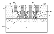
- FIG. 14A is a top down view of the exemplary semiconductor structure of FIGS. 13A-13B after replacing the sacrificial gate structure with a functional gate structure in accordance with an embodiment of the present application.
- FIG. 14B is a cross sectional view of the exemplary semiconductor structure of FIG. 14A along vertical plane B-B′.
- FIG. 15A is a top down view of the exemplary semiconductor structure of FIGS. 14A-14B after forming contact structures in the MOL dielectric material.
- FIG. 15B is a cross sectional view of the exemplary semiconductor structure of FIG. 15A along vertical plane B-B′.
- FIGS. 1A-1B there are illustrated various views of an exemplary semiconductor structure including, from bottom to top, a semiconductor material layer 10 and a hard mask layer 12 that can be employed in accordance with an embodiment of the present application.
- the semiconductor material layer 10 that can be employed in the present application includes any semiconductor material having semiconducting properties.
- semiconductor materials that can be employed as the semiconductor material layer 10 include, but are not limited to, silicon (Si), germanium (Ge), silicon germanium alloys (SiGe), silicon carbide (SiC), silicon germanium carbide (SiGeC), III-V compound semiconductors and/or II-VI compound semiconductors.
- III-V compound semiconductors are materials that include at least one element from Group III of the Periodic Table of Elements and at least one element from Group V of the Periodic Table of Elements.
- II-VI compound semiconductors are materials that include at least one element from Group II of the Periodic Table of Elements and at least one element from Group VI of the Periodic Table of Elements.
- the semiconductor material layer 10 that can be employed in the present application is typically a single crystalline semiconductor material such as, for example, single crystalline silicon.
- the semiconductor material layer 10 may have any of the well known crystal orientations.
- the crystal orientation of the semiconductor material layer 10 may be ⁇ 100 ⁇ , ⁇ 110 ⁇ , or ⁇ 111 ⁇ .
- Other crystallographic orientations besides those specifically mentioned can also be used in the present application.
- the semiconductor material layer 10 may represents an entirety of a bulk semiconductor substrate. In another embodiment of the present application, the semiconductor material layer 10 may represent a topmost semiconductor material of a stack of various semiconductor materials. In yet another embodiment of the present application, the semiconductor material layer 10 may represent a topmost semiconductor layer of a semiconductor-on-insulator (SOI) substrate. In such an embodiment (not specially shown), an insulator layer and, optionally, a handle substrate, may be located beneath the semiconductor material layer 10 .
- SOI semiconductor-on-insulator
- the handle substrate may include one of the semiconductor materials mentioned above for the semiconductor material layer 10 .
- the handle substrate may include a same semiconductor material as the semiconductor material layer 10 .
- the handle substrate may include a semiconductor material that is different in terms of composition from the semiconductor material that provides the semiconductor material layer 10 .
- the semiconductor material may be single crystalline, polycrystalline or amorphous.
- the handle substrate is a semiconductor material, the semiconductor material that provides the handle substrate may have any of the above mentioned crystal orientations.
- the handle substrate of the SOI may be composed of a non-semiconductor material including, for example, a dielectric material and/or a conductive material.
- the insulator layer of the SOI substrate may be a crystalline or non-crystalline dielectric material such as an oxide and/or nitride.
- the insulator layer of the SOI substrate is a dielectric oxide such as, for example, silicon dioxide.
- the insulator layer of the SOI substrate may be a dielectric nitride such as, for example, silicon nitride or boron nitride.
- the insulator layer of SOI substrate may include a stack of a dielectric oxide and a dielectric nitride.
- a stack of, in any order, silicon dioxide and silicon nitride or boron nitride may be employed as the insulator layer of the SOI substrate.
- the insulator layer of the SOI substrate may have a thickness from 10 nm to 200 nm, although other thicknesses that are lesser than, or greater than, the aforementioned thickness range may also be employed as the thickness of the insulator layer of the SOI substrate.
- the semiconductor material layer 10 may have a thickness from 10 nm to 200 nm. In other embodiments of the present application and for a bulk substrate, the semiconductor material layer 10 may have a thickness from 100 ⁇ m to 1000 ⁇ m. Other thicknesses that are lesser than, or greater than, the aforementioned thickness ranges may also be employed as the thickness of the semiconductor material layer 10 .
- the hard mask layer 12 is a contiguous layer that covers the entirety of the semiconductor material layer 10 .
- the hard mask layer 12 that is employed in the present application may include any hard mask material such as, for example, a dielectric oxide, a dielectric nitride and/or a dielectric oxynitride.
- the hard mask material that can be used in providing the hard mask layer 12 can be composed of silicon dioxide.
- the hard mask material that can be used in providing the hard mask layer 12 can be composed of silicon nitride.
- the hard mask material that can be used in providing the hard mask layer 12 can be a stack composed of, in any order, silicon dioxide and silicon nitride.
- the hard mask material that can be used in providing the hard mask layer 12 can be formed by a deposition process such as, for example, chemical vapor deposition (CVD) or plasma enhanced chemical vapor deposition (PECVD).
- the hard mask material that can be used in providing the hard mask layer 12 can be formed by a thermal process such as, for example, thermal oxidation and/or thermal nitridation.
- the hard mask material that can be used in providing the hard mask layer 12 can be formed by a combination of a deposition process and a thermal process.
- the thickness of the hard mask layer 12 can range from 10 nm to 40 nm. Other thicknesses that are lesser than, or greater than, the aforementioned thickness range may also be employed as the thickness of the hard mask layer 12 .
- FIGS. 2A-2B there are illustrated various views of the exemplary semiconductor structure of FIGS. 1A-1B after patterning the hard mask layer 12 .
- a portion of the hard mask layer 12 remains on the surface of the semiconductor material layer 10 .
- Each remaining portion of the hard mask layer 12 may be referred to herein as a hard mask portion 12 P.
- the patterning process used to define the exemplary semiconductor structure shown in FIGS. 2A-2B may include lithography and etching.
- Lithography includes forming a photoresist material (not shown) atop a material or material stack to be patterned.
- the photoresist material may include a positive-tone photoresist composition, a negative-tone photoresist composition or a hybrid-tone photoresist composition.
- the photoresist material may be formed by a deposition process such as, for example, spin-on coating. After forming the photoresist material, the deposited photoresist material is subjected to a pattern of irradiation. Next, the exposed photoresist material is developed utilizing a conventional resist developer.
- This provides a patterned photoresist atop a portion of the material or material stack to be patterned.
- the pattern provided by the patterned photoresist material is thereafter transferred into the underlying material layer or material layers utilizing at least one pattern transfer etching process.
- the at least one pattern transfer etching process is an anisotropic etch.
- a dry etching process such as, for example, reactive ion etching can be used.
- a chemical etchant can be used.
- a combination of dry etching and wet etching can be used.
- the patterned photoresist can be removed utilizing any photoresist stripping process such as, for example, ashing.
- the patterned photoresist may remain atop each hard mask portion 12 P during the subsequent patterning of the semiconductor material layer 10 . After patterning the semiconductor material layer 10 and, if not previously removed, the patterned photoresist may then be removed as defined above.
- the patterning process used to define the exemplary semiconductor structure shown in FIGS. 2A-2B may include a sidewall image transfer (SIT) process.
- the patterning process used to define the exemplary semiconductor structure shown in FIGS. 2A-2B may include a direct self-assembly (DSA) patterning process.
- Each hard mask portion 12 P that is formed can have a width, as measured from one sidewall to an opposing sidewall, of from 15 nm to 60 nm. Other widths are possible and can be employed in the present application for the width of each hard mask portion 12 P.
- Each hard mask portion 12 P has sidewall surfaces that are substantially perpendicular to the topmost horizontal surface of the semiconductor material layer 10 . By “substantially perpendicular” it is meant that the sidewall surfaces of each hard mask portion 12 P is 90° ⁇ 3° relative to the topmost horizontal surface of the semiconductor material layer 10 .
- FIGS. 3A-3B there are illustrated various views of the exemplary semiconductor structure of FIGS. 2A-2B after patterning the semiconductor material layer 10 to provide semiconductor pillars 10 P utilizing remaining portions of the hard mask layer (i.e., each hard mask portion 12 P) as an etch mask.
- the patterning process used to define the semiconductor pillars 10 P includes one of the etching steps mentioned above for etching the hard mask layer 12 .
- the patterning of the semiconductor material layer 10 includes an anisotropic etch such as, for example, a crystallographic preferential etch such as TMAH on silicon, to have an atomic smooth surface, or a reactive ion etch.
- the sidewall surface of the semiconductor pillar 10 P can be any crystal orientation.
- each semiconductor pillar 10 P sidewall surface be a (111) oriented surface.
- each semiconductor pillar 10 P extends upward from a remaining portion of the semiconductor material layer 10 .
- each semiconductor pillar extends upwards from an underlying semiconductor material layer or an insulator layer.
- Each semiconductor pillar 10 P has a width that is within the range mentioned above for each hard mask portion 12 P.
- Each semiconductor pillar 10 P may have a height from 10 nm to 100 nm. Other heights that are lesser than, or greater than, the aforementioned height range may also be employed as the height of each semiconductor pillar 10 P.
- each semiconductor pillar 10 P has sidewall surfaces that are vertically aligned to the sidewall surfaces of the corresponding overlying hard mask portion 12 P.
- FIGS. 4A-4B there are illustrated the exemplary semiconductor structure of FIGS. 3A-3B after forming a local isolation region 14 between each semiconductor pillar 10 P.
- Each local isolation region 14 is formed partially within a gap that is present between each semiconductor pillar 10 P such that each local isolation region 14 is formed surrounding a bottom sidewall portion of each semiconductor pillar 10 P.
- each local isolation region 14 does not extend to the height of each semiconductor pillar 10 P and thus an upper sidewall portion of each semiconductor pillar 10 P is bare at this point of the present application.
- a bottommost surface of each local isolation region 14 contacts a remaining portion of the semiconductor material layer 10 .
- the bottommost surface of each local isolation region 14 may contact the insulator layer of an SOI substrate, or, in the case of a stack of semiconductor materials, the bottommost surface of each local isolation region 14 may contact a semiconductor material other than the semiconductor material layer 10 .
- Each local isolation region 14 may be formed by first forming a trench dielectric material such as, for example, a trench oxide, utilizing a deposition process such as, for example, chemical vapor deposition or plasma enhanced chemical vapor deposition. The deposition process by itself may be sufficient to provide each local isolation region 14 .
- a planarization such as, for example, chemical mechanical polishing is first used, and thereafter an etch back step is then employed to provide the local isolation regions 14 .
- an etch back step is employed to provide the local isolation regions 14 .
- each spacer 16 has a bottommost surface that contacts a portion of a topmost surface of an underlying local isolation region 14 .
- Each spacer 16 also has a topmost surface that may be coplanar with a topmost surface of each hard mask portion 12 P.
- the spacer 16 does not fill the entirety of the gap that is located between each neighboring semiconductor pillar 10 P.
- Each spacer 16 is composed of a spacer dielectric material that has a different etch rate than at least the hard mask material that provides each hard mask portion 12 P.
- spacer dielectric material that provides each spacer 16 may be composed of silicon dioxide, while each hard mask portion 12 P may be composed of silicon nitride.
- Each sacrificial spacer 16 may be formed by first depositing a contiguous layer of the spacer dielectric material, and thereafter subjecting the contiguous layer of the spacer dielectric material to a spacer etching process.
- the thickness of each spacer 16 can be from 2 nm to 20 nm thick. Other thicknesses that are lesser than 2 nm, or greater than 20 nm can be used.
- the patterned resist 18 may be composed of one of the photoresist material mentioned above for patterning the hard mask layer 12 .
- the patterned resist 18 may be formed by first forming the photoresist material by utilizing a deposition process such as, for example, spin-on coating, and thereafter subjecting the photoresist material to photolithography (i.e., EUV exposure and development).
- photolithography i.e., EUV exposure and development.
- Each opening 20 exposes at least one area in which a semiconductor pillar 10 P is present.
- the openings 20 are formed over an entire semiconductor pillar 10 P, while other openings 20 are formed over a portion of a semiconductor pillar 10 P. As is shown in the top down views, the openings 20 within the patterned resist 18 are orientated in a staggered configuration between each neighboring pair of semiconductor pillars 10 P.
- Each opening 20 may have a first width that can be in a range from 5 nm to 40 nm. Other first widths that are lesser than, or greater, than the aforementioned first width are also possible in the present application.
- FIGS. 7A-7B there are illustrated various views of the exemplary semiconductor structure of FIGS. 6A-6B after forming a sacrificial material 22 along the sidewalls of the patterned resist 18 in the openings 20 so as to shrink the dimension of the openings 20 .
- this step of forming the sacrificial material 22 can be omitted.
- the sacrificial material 22 may be composed of amorphous carbon.
- Other materials can also be employed in the present application as the material that provides the sacrificial material 22 so long as the sacrificial material 22 is different in composition from the spacer 16 . Examples include a porous oxide material.
- the sacrificial material 22 may be formed by a deposition process. An optional etch may follow the deposition of the material that provides the sacrificial material 22 .
- Each opening 20 containing the sacrificial material 22 may have a second width that is less than the first width.
- FIGS. 8A-8B there are illustrated the exemplary semiconductor structure of FIGS. 7A-7B after providing a seed hole 24 in each of the spacers 16 to expose a portion of a sidewall surface of each semiconductor pillar 10 P and removing the patterned resist 18 and, if present the sacrificial material 22 .
- the seed hole 24 can be formed into each of the spacers 16 utilizing a wet etching process that is selective in removing the spacer dielectric material that provides each spacer 16 .
- hydrofluoric acid can be used to provide each seed hole 24 .
- the patterned resist 18 and, if present the sacrificial material 22 may be removed utilizing conventional processes that are well known to those skilled in the art.
- the portion of the sidewall surface of each semiconductor pillar 10 P that is exposed by the seed hole 24 will be used as a seed material for the subsequent growth of a semiconductor nanowire.
- FIGS. 9A-9B there are illustrated various views of the exemplary semiconductor structure of FIGS. 8A-8B after epitaxially growing (or depositing) a semiconductor nanowire 26 laterally outward from the exposed sidewalls of each semiconductor pillar 10 P and through each seed hole 24 .
- Each semiconductor nanowire 26 is oriented parallel to each other.
- each semiconductor nanowire 26 that is formed has one end 26 X that is located in a seed hole 24 of one of the spacers, and another end 26 Y that directly contacts a remaining portion of a spacer that is present on a neighboring semiconductor pillar.
- the end 26 X of each semiconductor nanowire that is in the seed hole 24 directly contacts the exposed sidewall of one of the semiconductor pillars.
- the semiconductor nanowire that is formed utilizing the method of the present application has fewer defects than prior art methods.
- epitaxial growth and/or deposition and “epitaxially formed and/or grown” mean the growth of a semiconductor material on a deposition surface of a semiconductor material, in which the semiconductor material being grown has the same crystalline characteristics as the semiconductor material of the deposition surface.
- the chemical reactants provided by the source gases are controlled and the system parameters are set so that the depositing atoms arrive at the deposition surface of the semiconductor substrate with sufficient energy to move around on the surface and orient themselves to the crystal arrangement of the atoms of the deposition surface. Therefore, an epitaxial semiconductor material has the same crystalline characteristics as the deposition surface on which it is formed.
- each semiconductor nanowire 26 has an epitaxial relationship with the growth surface (i.e., exposed sidewall portion) of the semiconductor pillar 10 P.
- Examples of various epitaxial growth process apparatuses that can be employed in the present application include, e.g., rapid thermal chemical vapor deposition (RTCVD), low-energy plasma deposition (LEPD), ultra-high vacuum chemical vapor deposition (UHVCVD), atmospheric pressure chemical vapor deposition (APCVD) and molecular beam epitaxy (MBE).
- RTCVD rapid thermal chemical vapor deposition
- LEPD low-energy plasma deposition
- UHVCVD ultra-high vacuum chemical vapor deposition
- APCVD atmospheric pressure chemical vapor deposition
- MBE molecular beam epitaxy
- the temperature for epitaxial deposition typically ranges from 550° C. to 900° C. Although higher temperature typically results in faster deposition, the faster deposition may result in crystal defects and film cracking.
- the epitaxial growth of each semiconductor nanowire 26 can be performed utilizing any well known precursor gas or gas mixture. Carrier gases like hydrogen, nitrogen, helium and argon can be used.
- Each semiconductor nanowire 26 is composed of one of the semiconductor materials mentioned above for the semiconductor material layer 10 .
- each semiconductor nanowire 26 is composed of a same semiconductor material as that which provides the semiconductor material layer 10 .
- the semiconductor material layer 10 (and hence the semiconductor pillars 10 P) and the semiconductor nanowires 26 may each be composed of silicon.
- each semiconductor nanowire is composed of a different semiconductor material than that which provides the semiconductor material layer 10 .
- the semiconductor material layer 10 (and hence the semiconductor pillars 10 P) may be composed of silicon, while the semiconductor nanowires 26 may be composed of a high mobility channel material such as, for example, a III-V compound semiconductor.
- Each semiconductor nanowire 26 may have width from 2 nm to 40 nm, a length from 20 nm to 200 nm, and a height from 10 nm to 40 nm. Other dimensions (i.e., width, length and height) are possible for each semiconductor nanowire 26 . In some embodiments, a wet etch or any other semiconductor nanowire thinning step may be performed to reduce the dimensions of each semiconductor nanowire 26 .
- FIGS. 10A-10B there are illustrated various views of the exemplary semiconductor structure of FIGS. 9A-9B after forming a sacrificial gate structure 28 straddling over a portion of each semiconductor nanowire 26 .
- straddling it is meant that the sacrificial gate structure 28 is present on each side of a semiconductor nanowire 26 and has a portion that is present atop a semiconductor nanowire 26 .
- the portion of the semiconductor nanowire that the sacrificial gate structure (and the subsequently formed functional gate structure) is present may be referred to herein as a channel portion (or channel region).
- the sacrificial gate structures 28 and hence the functional gate structure are orientated perpendicular to each semiconductor nanowire 26 .
- each sacrificial gate structure 28 can include, from bottom to top, of sacrificial dielectric material and a sacrificial gate material. In another embodiment, each gate sacrificial gate structure 28 may include only the sacrificial gate material.
- the sacrificial gate dielectric material may include an oxide, nitride, and/or oxynitride.
- the sacrificial gate dielectric material may be composed of silicon dioxide and/or silicon nitride.
- the sacrificial gate material can include any material that can be selectively removed from the structure during a subsequently performed etching process.
- the sacrificial gate material may be composed of polysilicon.
- the sacrificial gate material may be composed of a metal such as, for example, Al, W, or Cu.
- Each sacrificial gate structure 28 is formed by depositing the material or materials that provide a sacrificial gate stack and thereafter an etch can be used to pattern the sacrificial gate stack.
- Each sacrificial gate stack 28 can have a thickness from 50 nm to 300 nm, although lesser and greater thicknesses can also be employed.
- a functional gate structure as defined herein below is formed instead of the sacrificial gate structures. Also, and in other embodiments (not shown), a first set of sacrificial gate structures is formed straddling over some of the semiconductor nanowires, while a first set of functional gate structure is formed straddling over other semiconductor nanowires. In such instances, block mask technology may be employed to form the sacrificial gate structures and functional gate structures at this point of the present application.
- Each source/drain structure includes an upper portion 30 U and a lower portion 30 L.
- the lower portion 30 L of each source/drain structure includes a doped portion of the semiconductor nanowire 26 not protected by the sacrificial gate structure 28 and thus adjacent to the channel portion of the semiconductor nanowire.
- the upper portion 30 U of each source/drain includes a doped semiconductor material that is epitaxially grown on the exposed portions of the semiconductor nanowire 26 not protected by the sacrificial gate structure 28 .
- Each source/drain structure ( 30 U, 30 L) can be formed by first providing the doped semiconductor material by utilizing an epitaxial growth process as mentioned above.
- the semiconductor material that forms the upper portion 30 U of each source/drain structure may include one of the semiconductor materials mentioned above for the semiconductor material layer 10 .
- the semiconductor material that provides the upper portion 30 U of each source/drain structure may be a same semiconductor material as the semiconductor material that provides each semiconductor nanowire 26 .
- the semiconductor material that provides the upper portion 30 U of each source/drain structure may be a different semiconductor material than the semiconductor material that provides each semiconductor nanowire 26 .
- the dopant that is present in the doped semiconductor material that provides the upper portion 30 U of each source/drain structure may be a p-type dopant or an n-type dopant.
- p-type refers to the addition of impurities to an intrinsic semiconductor that creates deficiencies of valence electrons.
- examples of p-type dopants, i.e., impurities include, but are not limited to, boron, aluminum, gallium and indium.
- N-type refers to the addition of impurities that contributes free electrons to an intrinsic semiconductor.
- n-type dopants i.e., impurities
- examples of n-type dopants include, but are not limited to, antimony, arsenic and phosphorous.
- the dopant of the upper portion 30 U of each source/drain structure may introduce into the precursor source gas used to epitaxially grow the doped semiconductor material.
- the dopant of the upper portion 30 U of each source/drain structure may introduced into an intrinsically grown semiconductor material utilizing one of ion implantation or gas phase doping.
- the upper portion 30 U of each source/drain structure may have a dopant concentration that can be within a range from 1 ⁇ 10 19 atoms/cm 3 to 1 ⁇ 10 21 atoms/cm 3 .
- the lower portion 30 L of each source/drain structure can be formed by diffusion of dopants from the upper portion 30 U into the underlying portion of the semiconductor nanowires 26 that are not protected by the sacrificial gate structure 28 .
- the diffusion of dopants may be performed utilizing an annealing process that causes diffusion of dopants from one material to another material.
- a thermal anneal performed at a temperature from 300° C. to 1100° C. may be performed.
- the lower portion 30 L of each source/drain structure may have a dopant concentration that can be within a range from 1 ⁇ 10 19 atoms/cm 3 to 1 ⁇ 10 21 atoms/cm 3 .
- a gate spacer may be formed around each sacrificial gate structure 28 prior to forming the source/drain structures ( 30 U, 20 L).
- the gate spacer may include one of the dielectric spacer materials mentioned above for spacer 16 , and the gate spacer may be formed utilizing the same technique as mentioned above for forming spacer 16 .
- FIGS. 12A-12B there are illustrated various views of the exemplary semiconductor structure of FIGS. 11A-11B after removing a portion of each semiconductor pillar 10 P.
- the removal of a portion of each semiconductor pillar 10 P may be performed utilizing an etching process that is selective in removing the semiconductor material that provides the semiconductor pillar 10 P.
- a planarization process may be employed.
- the hard mask portion 12 P Prior to removing a portion of each semiconductor pillar 10 P, the hard mask portion 12 P is entirely removed utilizing an etch that is selective in removing the hard mask material that provides each hard mask portion 12 P. As is shown in the illustrated embodiment, a portion of each semiconductor pillar 10 P remains.
- Each remaining portion of the semiconductor pillar 10 P can be referred to herein as a mesa portion 10 M of a semiconductor material (which is the same as semiconductor material layer 10 mentioned above).
- Each mesa portions 10 M has a topmost surface that is coplanar with a topmost surface of each local isolation region 14 .
- FIGS. 13A-13B there are illustrated various views of the exemplary semiconductor structure of FIGS. 12A-12B after forming a middle-of the-line (MOL) dielectric material 32 .
- the MOL dielectric material 32 has a topmost most surface that is coplanar with a topmost surface of each sacrificial gate structure 26 .
- the MOL dielectric material 32 may be composed of, for example, silicon dioxide, undoped silicate glass (USG), fluorosilicate glass (FSG), borophosphosilicate glass (BPSG), a spin-on low-k dielectric layer, a chemical vapor deposition (CVD) low-k dielectric layer or any combination thereof.
- low-k denotes a dielectric material that has a dielectric constant of less than silicon dioxide.
- a self-planarizing material such as a spin-on glass (SOG) or a spin-on low-k dielectric material such as SiLKTM can be used as the MOL dielectric material 32 .
- the use of a self-planarizing dielectric material as MOL dielectric material 32 may avoid the need to perform a subsequent planarizing step.
- the MOL dielectric material 32 can be formed utilizing a deposition process including, for example, chemical vapor deposition (CVD), plasma enhanced chemical vapor deposition (PECVD), evaporation or spin-on coating.
- CVD chemical vapor deposition
- PECVD plasma enhanced chemical vapor deposition
- evaporation or spin-on coating evaporation or spin-on coating.
- a planarization process or an etch back process follows the deposition of the dielectric material.
- the thickness of the MOL dielectric material 32 that can be employed in the present application may vary depending on the type of dielectric material employed as well as the method that was employed in forming the same. In one embodiment, the MOL dielectric material 32 has a thickness from 80 nm to 500 nm. Other thicknesses that are greater or lesser than the range provided above can also be used for the MOL dielectric material 32 .
- FIGS. 14A-14B there are illustrated various views of the exemplary semiconductor structure of FIGS. 13A-13B after replacing the sacrificial gate structure 28 with a functional gate structure 34 in accordance with an embodiment of the present application.
- the step of the present application may be skipped in instances in which the gate structure previously formed in FIGS. 10A-10B is a functional gate structure.
- Each sacrificial gate structure 28 may be replaced utilizing an anisotropic etching process such as, for example, reactive ion etching.
- the removal of each sacrificial gate structure 28 forms a gate cavity in which a functional gate structure will be subsequently formed.
- the gate cavity exposed the channel portion of the semiconductor nanowire 26 .
- each first functional gate 34 includes a gate dielectric portion (not shown) and a gate conductor portion (not shown).
- the gate dielectric portion of each functional gate structure 34 may include a gate dielectric material.
- the gate dielectric material that provides the gate dielectric portion of each functional gate structure 34 can be an oxide, nitride, and/or oxynitride.
- the gate dielectric material that provides the gate dielectric portion can be a high-k material having a dielectric constant greater than silicon dioxide.
- Exemplary high-k dielectrics include, but are not limited to, HfO 2 , ZrO 2 , La 2 O 3 , Al 2 O 3 , TiO 2 , SrTiO 3 , LaAlO 3 , Y 2 O 3 , HfO x N y , ZrO x N y , La 2 O x N y , Al 2 O x N y , TiO x N y , SrTiO x N y , LaAlO x N y , Y 2 O x N y , SiON, SiN x , a silicate thereof, and an alloy thereof.
- a multilayered gate dielectric structure comprising different gate dielectric materials, e.g., silicon dioxide, and a high-k gate dielectric, can be formed and used as the gate dielectric portion.
- a first set of functional gate structures includes a first gate dielectric portion, while a second set of functional gate structures comprises a second gate dielectric portion.
- the first gate dielectric material portion of each first functional gate structure of the first and second sets of functional gate structures may be the same as, or different from, the second gate dielectric material portion.
- the gate dielectric material used in providing the gate dielectric portion of each functional gate structure 34 can be formed by any deposition process including, for example, chemical vapor deposition (CVD), plasma enhanced chemical vapor deposition (PECVD), physical vapor deposition (PVD), sputtering, or atomic layer deposition.
- CVD chemical vapor deposition
- PECVD plasma enhanced chemical vapor deposition
- PVD physical vapor deposition
- sputtering or atomic layer deposition.
- block mask technology can be used.
- the gate dielectric material used in providing the gate dielectric portion can have a thickness in a range from 1 nm to 10 nm. Other thicknesses that are lesser than, or greater than, the aforementioned thickness range can also be employed for the gate dielectric material that may provide the gate dielectric portion.
- the gate conductor portion of each functional gate structure 34 can include a gate conductor material.
- the gate conductor material used in providing the gate conductor portion of each functional gate structure 34 can include any conductive material including, for example, doped polysilicon, an elemental metal (e.g., tungsten, titanium, tantalum, aluminum, nickel, ruthenium, palladium and platinum), an alloy of at least two elemental metals, an elemental metal nitride (e.g., tungsten nitride, aluminum nitride, and titanium nitride), an elemental metal silicide (e.g., tungsten silicide, nickel silicide, and titanium silicide) or multilayered combinations thereof.
- an elemental metal e.g., tungsten, titanium, tantalum, aluminum, nickel, ruthenium, palladium and platinum
- an alloy of at least two elemental metals e.g., tungsten nitride, aluminum nitride, and titanium n
- a first set of functional gate structures includes a first gate conductor portion, while a second set of functional gate structures comprises a second gate conductor portion.
- the first gate conductor portion may be the same as, or different from, the second gate conductor portion.
- the first gate conductor portion may comprise an nFET gate metal
- the second gate conductor portion may comprise a pFET gate metal
- the first gate conductor portion may comprise a pFET gate metal
- the second gate conductor portion may comprise an nFET gate metal.
- the gate conductor material used in providing the gate conductor portion can be formed utilizing a deposition process including, for example, chemical vapor deposition (CVD), plasma enhanced chemical vapor deposition (PECVD), physical vapor deposition (PVD), sputtering, atomic layer deposition (ALD) or other like deposition processes.
- CVD chemical vapor deposition
- PECVD plasma enhanced chemical vapor deposition
- PVD physical vapor deposition
- sputtering atomic layer deposition
- ALD atomic layer deposition
- a metal silicide is formed
- a different gate conductor material is used for gate conductor portions of different functional gate structures, block mask technology can be used.
- the gate conductor material used in providing the gate conductor portion has a thickness from 50 nm to 200 nm. Other thicknesses that are lesser than, or greater than, the aforementioned thickness range can also be employed for the gate conductor material used in providing the gate conductor portion.
- Each functional gate structure 34 can be formed by first providing a gate dielectric material and a gate conductor material, and thereafter a planarization process such as, for example, chemical mechanical polishing (CMP) can be used.
- CMP chemical mechanical polishing
- the gate dielectric material portion of the functional gate structure 34 may be U-shaped and the gate conductor material portion may be confined within the U-shaped gate dielectric material portion of the functional gate structure 34 .
- the contact structure 36 can be formed by first providing a contact opening within the MOL dielectric material 32 utilizing lithography and etching.
- a contact metal such as, for example, tungsten, copper, aluminum or alloys thereof is then formed within each contact opening by utilizing a conventional deposition process.
- a planarization process may follow the deposition of the contact metal.
- one of the contact structures 36 contacts a sidewall of an upper portion 30 U and a lower portion 30 L of one of the source/drain structures.
Abstract
A method is provided that may include providing a plurality of semiconductor pillars extending from a surface of a substrate, wherein a spacer is present on sidewall surfaces of each semiconductor pillar. A seed hole is then formed in a portion of each spacer that exposes a portion of at least one sidewall surface of each semiconductor pillar. Next, a semiconductor nanowire is epitaxially grown from the exposed portion of the at least one sidewall surface of each semiconductor pillar and entirely through each seed hole. A gate structure is then formed straddling over a channel portion of each semiconductor nanowire.
Description
The present application relates to a semiconductor structure and a method of forming a semiconductor structure. More particularly, the present application relates to a method of forming a semiconductor nanowire laterally from a portion of a sidewall of a semiconductor pillar.
For more than three decades, the continued miniaturization of metal oxide semiconductor field effect transistors (MOSFETs) has driven the worldwide semiconductor industry. Various showstoppers to continued scaling have been predicated for decades, but a history of innovation has sustained Moore's Law in spite of many challenges. However, there are growing signs today that metal oxide semiconductor transistors are beginning to reach their traditional scaling limits. Since it has become increasingly difficult to improve MOSFETs and therefore complementary metal oxide semiconductor (CMOS) performance through continued scaling, further methods for improving performance in addition to scaling have become critical.
The use of non-planar semiconductor devices such as, for example, semiconductor nanowire field effect transistors is the next step in the evolution of complementary metal oxide semiconductor (CMOS) devices. In its basic form, semiconductor nanowire field effect transistors include at least one semiconductor nanowire including a source region, a drain region and a channel region located between the source region and the drain region, and a gate electrode that is formed straddling over the channel region of the at least one semiconductor nanowire. A gate dielectric is typically disposed between the channel region of the at least one semiconductor nanowire and the gate electrode. The gate electrode regulates electron flow through the semiconductor nanowire channel between the source region and the drain region.
Semiconductor nanowire field effect transistors can achieve higher drive currents with increasingly smaller dimensions as compared to conventional planar FETs. One problem associated with conventional semiconductor nanowire field effect transistors that include high mobility channel materials such as, a III-V compound semiconductor, is that the semiconductor nanowire that is grown typically has defects associated therewith which hinder the performance of the device.
One aspect of the present application relates to a method of forming a semiconductor structure. In one embodiment of the present application, the method may include providing a plurality of semiconductor pillars extending from a surface of a substrate, wherein a spacer is present on sidewall surfaces of each semiconductor pillar. A seed hole is then formed in a portion of each spacer that exposes a portion of at least one sidewall surface of each semiconductor pillar. Next, a semiconductor nanowire is epitaxially grown from the exposed portion of the at least one sidewall surface of each semiconductor pillar and entirely through each seed hole. A gate structure is then formed straddling over a channel portion of each semiconductor nanowire.
Another aspect of the present application relates to a semiconductor structure. In one embodiment of the present application, the semiconductor structure may include a plurality of semiconductor nanowires oriented parallel to each other, wherein one end of each of the semiconductor nanowires is present in a seed hole provided in a first spacer, and another end of each of the semiconductor nanowires contacts a sidewall surface of a second spacer. The structure of the present application further includes a functional gate structure oriented perpendicular to and straddling over a channel portion of each of the semiconductor nanowires.
The present application will now be described in greater detail by referring to the following discussion and drawings that accompany the present application. It is noted that the drawings of the present application are provided for illustrative purposes only and, as such, the drawings are not drawn to scale. It is also noted that like and corresponding elements are referred to by like reference numerals.
In the following description, numerous specific details are set forth, such as particular structures, components, materials, dimensions, processing steps and techniques, in order to provide an understanding of the various embodiments of the present application. However, it will be appreciated by one of ordinary skill in the art that the various embodiments of the present application may be practiced without these specific details. In other instances, well-known structures or processing steps have not been described in detail in order to avoid obscuring the present application.
It will be understood that when an element as a layer, region or substrate is referred to as being “on” or “over” another element, it can be directly on the other element or intervening elements may also be present. In contrast, when an element is referred to as being “directly on” or “directly over” another element, there are no intervening elements present. It will also be understood that when an element is referred to as being “beneath” or “under” another element, it can be directly beneath or under the other element, or intervening elements may be present. In contrast, when an element is referred to as being “directly beneath” or “directly under” another element, there are no intervening elements present.
Referring first to FIGS. 1A-1B , there are illustrated various views of an exemplary semiconductor structure including, from bottom to top, a semiconductor material layer 10 and a hard mask layer 12 that can be employed in accordance with an embodiment of the present application.
The semiconductor material layer 10 that can be employed in the present application includes any semiconductor material having semiconducting properties. Examples of semiconductor materials that can be employed as the semiconductor material layer 10 include, but are not limited to, silicon (Si), germanium (Ge), silicon germanium alloys (SiGe), silicon carbide (SiC), silicon germanium carbide (SiGeC), III-V compound semiconductors and/or II-VI compound semiconductors. III-V compound semiconductors are materials that include at least one element from Group III of the Periodic Table of Elements and at least one element from Group V of the Periodic Table of Elements. II-VI compound semiconductors are materials that include at least one element from Group II of the Periodic Table of Elements and at least one element from Group VI of the Periodic Table of Elements.
The semiconductor material layer 10 that can be employed in the present application is typically a single crystalline semiconductor material such as, for example, single crystalline silicon. The semiconductor material layer 10 may have any of the well known crystal orientations. For example, the crystal orientation of the semiconductor material layer 10 may be {100}, {110}, or {111}. Other crystallographic orientations besides those specifically mentioned can also be used in the present application.
In one embodiment of the present application, the semiconductor material layer 10 may represents an entirety of a bulk semiconductor substrate. In another embodiment of the present application, the semiconductor material layer 10 may represent a topmost semiconductor material of a stack of various semiconductor materials. In yet another embodiment of the present application, the semiconductor material layer 10 may represent a topmost semiconductor layer of a semiconductor-on-insulator (SOI) substrate. In such an embodiment (not specially shown), an insulator layer and, optionally, a handle substrate, may be located beneath the semiconductor material layer 10.
When present, the handle substrate may include one of the semiconductor materials mentioned above for the semiconductor material layer 10. In some embodiments, the handle substrate may include a same semiconductor material as the semiconductor material layer 10. In other embodiments, the handle substrate may include a semiconductor material that is different in terms of composition from the semiconductor material that provides the semiconductor material layer 10. When the handle substrate is a semiconductor material, the semiconductor material may be single crystalline, polycrystalline or amorphous. When the handle substrate is a semiconductor material, the semiconductor material that provides the handle substrate may have any of the above mentioned crystal orientations. In another embodiment of the present application, the handle substrate of the SOI may be composed of a non-semiconductor material including, for example, a dielectric material and/or a conductive material.
The insulator layer of the SOI substrate may be a crystalline or non-crystalline dielectric material such as an oxide and/or nitride. In one embodiment, the insulator layer of the SOI substrate is a dielectric oxide such as, for example, silicon dioxide. In another embodiment of the present application, the insulator layer of the SOI substrate may be a dielectric nitride such as, for example, silicon nitride or boron nitride. In yet another embodiment of the present application, the insulator layer of SOI substrate may include a stack of a dielectric oxide and a dielectric nitride. In one example, a stack of, in any order, silicon dioxide and silicon nitride or boron nitride may be employed as the insulator layer of the SOI substrate. The insulator layer of the SOI substrate may have a thickness from 10 nm to 200 nm, although other thicknesses that are lesser than, or greater than, the aforementioned thickness range may also be employed as the thickness of the insulator layer of the SOI substrate.
In some embodiments of the present application and for a SOI wafer, the semiconductor material layer 10 may have a thickness from 10 nm to 200 nm. In other embodiments of the present application and for a bulk substrate, the semiconductor material layer 10 may have a thickness from 100 μm to 1000 μm. Other thicknesses that are lesser than, or greater than, the aforementioned thickness ranges may also be employed as the thickness of the semiconductor material layer 10.
The hard mask layer 12 is a contiguous layer that covers the entirety of the semiconductor material layer 10. The hard mask layer 12 that is employed in the present application may include any hard mask material such as, for example, a dielectric oxide, a dielectric nitride and/or a dielectric oxynitride. In one embodiment, the hard mask material that can be used in providing the hard mask layer 12 can be composed of silicon dioxide. In another embodiment, the hard mask material that can be used in providing the hard mask layer 12 can be composed of silicon nitride. In yet another embodiment, the hard mask material that can be used in providing the hard mask layer 12 can be a stack composed of, in any order, silicon dioxide and silicon nitride.
In some embodiments, the hard mask material that can be used in providing the hard mask layer 12 can be formed by a deposition process such as, for example, chemical vapor deposition (CVD) or plasma enhanced chemical vapor deposition (PECVD). In other embodiments, the hard mask material that can be used in providing the hard mask layer 12 can be formed by a thermal process such as, for example, thermal oxidation and/or thermal nitridation. In yet other embodiments, the hard mask material that can be used in providing the hard mask layer 12 can be formed by a combination of a deposition process and a thermal process. The thickness of the hard mask layer 12 can range from 10 nm to 40 nm. Other thicknesses that are lesser than, or greater than, the aforementioned thickness range may also be employed as the thickness of the hard mask layer 12.
Referring now to FIGS. 2A-2B , there are illustrated various views of the exemplary semiconductor structure of FIGS. 1A-1B after patterning the hard mask layer 12. After patterning, and as shown in FIGS. 2A-2B , a portion of the hard mask layer 12 remains on the surface of the semiconductor material layer 10. Each remaining portion of the hard mask layer 12 may be referred to herein as a hard mask portion 12P.
The patterning process used to define the exemplary semiconductor structure shown in FIGS. 2A-2B may include lithography and etching. Lithography includes forming a photoresist material (not shown) atop a material or material stack to be patterned. The photoresist material may include a positive-tone photoresist composition, a negative-tone photoresist composition or a hybrid-tone photoresist composition. The photoresist material may be formed by a deposition process such as, for example, spin-on coating. After forming the photoresist material, the deposited photoresist material is subjected to a pattern of irradiation. Next, the exposed photoresist material is developed utilizing a conventional resist developer. This provides a patterned photoresist atop a portion of the material or material stack to be patterned. The pattern provided by the patterned photoresist material is thereafter transferred into the underlying material layer or material layers utilizing at least one pattern transfer etching process. Typically, the at least one pattern transfer etching process is an anisotropic etch. In one embodiment, a dry etching process such as, for example, reactive ion etching can be used. In another embodiment, a chemical etchant can be used. In still a further embodiment, a combination of dry etching and wet etching can be used. After etching, the patterned photoresist can be removed utilizing any photoresist stripping process such as, for example, ashing. In some embodiments, the patterned photoresist may remain atop each hard mask portion 12P during the subsequent patterning of the semiconductor material layer 10. After patterning the semiconductor material layer 10 and, if not previously removed, the patterned photoresist may then be removed as defined above.
In another embodiment, the patterning process used to define the exemplary semiconductor structure shown in FIGS. 2A-2B may include a sidewall image transfer (SIT) process. In yet another embodiment, the patterning process used to define the exemplary semiconductor structure shown in FIGS. 2A-2B may include a direct self-assembly (DSA) patterning process.
Each hard mask portion 12P that is formed can have a width, as measured from one sidewall to an opposing sidewall, of from 15 nm to 60 nm. Other widths are possible and can be employed in the present application for the width of each hard mask portion 12P. Each hard mask portion 12P has sidewall surfaces that are substantially perpendicular to the topmost horizontal surface of the semiconductor material layer 10. By “substantially perpendicular” it is meant that the sidewall surfaces of each hard mask portion 12P is 90°±3° relative to the topmost horizontal surface of the semiconductor material layer 10.
Referring now to FIGS. 3A-3B , there are illustrated various views of the exemplary semiconductor structure of FIGS. 2A-2B after patterning the semiconductor material layer 10 to provide semiconductor pillars 10P utilizing remaining portions of the hard mask layer (i.e., each hard mask portion 12P) as an etch mask. The patterning process used to define the semiconductor pillars 10P includes one of the etching steps mentioned above for etching the hard mask layer 12. In one embodiment, the patterning of the semiconductor material layer 10 includes an anisotropic etch such as, for example, a crystallographic preferential etch such as TMAH on silicon, to have an atomic smooth surface, or a reactive ion etch. The sidewall surface of the semiconductor pillar 10P can be any crystal orientation. For some cases for example, it may be preferred to have each semiconductor pillar 10P sidewall surface be a (111) oriented surface. In the illustrated embodiment, each semiconductor pillar 10P extends upward from a remaining portion of the semiconductor material layer 10. In other embodiments (not shown), each semiconductor pillar extends upwards from an underlying semiconductor material layer or an insulator layer.
Each semiconductor pillar 10P has a width that is within the range mentioned above for each hard mask portion 12P. Each semiconductor pillar 10P may have a height from 10 nm to 100 nm. Other heights that are lesser than, or greater than, the aforementioned height range may also be employed as the height of each semiconductor pillar 10P. In some embodiments and as shown, each semiconductor pillar 10P has sidewall surfaces that are vertically aligned to the sidewall surfaces of the corresponding overlying hard mask portion 12P.
Referring now to FIGS. 4A-4B , there are illustrated the exemplary semiconductor structure of FIGS. 3A-3B after forming a local isolation region 14 between each semiconductor pillar 10P. Each local isolation region 14 is formed partially within a gap that is present between each semiconductor pillar 10P such that each local isolation region 14 is formed surrounding a bottom sidewall portion of each semiconductor pillar 10P.
The height of each local isolation region 14 does not extend to the height of each semiconductor pillar 10P and thus an upper sidewall portion of each semiconductor pillar 10P is bare at this point of the present application. In some embodiments and as shown, a bottommost surface of each local isolation region 14 contacts a remaining portion of the semiconductor material layer 10. In yet another embodiment (not shown), the bottommost surface of each local isolation region 14 may contact the insulator layer of an SOI substrate, or, in the case of a stack of semiconductor materials, the bottommost surface of each local isolation region 14 may contact a semiconductor material other than the semiconductor material layer 10.
Each local isolation region 14 may be formed by first forming a trench dielectric material such as, for example, a trench oxide, utilizing a deposition process such as, for example, chemical vapor deposition or plasma enhanced chemical vapor deposition. The deposition process by itself may be sufficient to provide each local isolation region 14.
In some embodiments, and when the deposited trench dielectric material is formed above the topmost surface of each hard mask portion 12P, a planarization such as, for example, chemical mechanical polishing is first used, and thereafter an etch back step is then employed to provide the local isolation regions 14. In other embodiments, and when the deposited trench dielectric material is formed at or above the topmost surface of each semiconductor pillar 10, an etch back step is employed to provide the local isolation regions 14.
Referring now to FIGS. 5A-5B , there are illustrated the exemplary semiconductor structure of FIGS. 4A-4B after forming a spacer 16 along at least exposed sidewalls of each semiconductor pillar 10P. As is shown, each spacer 16 has a bottommost surface that contacts a portion of a topmost surface of an underlying local isolation region 14. Each spacer 16 also has a topmost surface that may be coplanar with a topmost surface of each hard mask portion 12P. As is further shown, the spacer 16 does not fill the entirety of the gap that is located between each neighboring semiconductor pillar 10P.
Each spacer 16 is composed of a spacer dielectric material that has a different etch rate than at least the hard mask material that provides each hard mask portion 12P. In one example, spacer dielectric material that provides each spacer 16 may be composed of silicon dioxide, while each hard mask portion 12P may be composed of silicon nitride. Each sacrificial spacer 16 may be formed by first depositing a contiguous layer of the spacer dielectric material, and thereafter subjecting the contiguous layer of the spacer dielectric material to a spacer etching process. The thickness of each spacer 16 can be from 2 nm to 20 nm thick. Other thicknesses that are lesser than 2 nm, or greater than 20 nm can be used.
Referring now to FIGS. 6A-6B , there are illustrated various views of the exemplary semiconductor structure of FIGS. 5A-5B after forming a patterned resist 18 containing openings 20 formed therein. The patterned resist 18 may be composed of one of the photoresist material mentioned above for patterning the hard mask layer 12. The patterned resist 18 may be formed by first forming the photoresist material by utilizing a deposition process such as, for example, spin-on coating, and thereafter subjecting the photoresist material to photolithography (i.e., EUV exposure and development). Each opening 20 exposes at least one area in which a semiconductor pillar 10P is present. As is shown, some of the openings 20 are formed over an entire semiconductor pillar 10P, while other openings 20 are formed over a portion of a semiconductor pillar 10P. As is shown in the top down views, the openings 20 within the patterned resist 18 are orientated in a staggered configuration between each neighboring pair of semiconductor pillars 10P.
Each opening 20 may have a first width that can be in a range from 5 nm to 40 nm. Other first widths that are lesser than, or greater, than the aforementioned first width are also possible in the present application.
Referring now to FIGS. 7A-7B , there are illustrated various views of the exemplary semiconductor structure of FIGS. 6A-6B after forming a sacrificial material 22 along the sidewalls of the patterned resist 18 in the openings 20 so as to shrink the dimension of the openings 20. In some embodiments, this step of forming the sacrificial material 22 can be omitted.
In one embodiment of the present application, the sacrificial material 22 may be composed of amorphous carbon. Other materials can also be employed in the present application as the material that provides the sacrificial material 22 so long as the sacrificial material 22 is different in composition from the spacer 16. Examples include a porous oxide material. The sacrificial material 22 may be formed by a deposition process. An optional etch may follow the deposition of the material that provides the sacrificial material 22. Each opening 20 containing the sacrificial material 22 may have a second width that is less than the first width.
Referring now to FIGS. 8A-8B , there are illustrated the exemplary semiconductor structure of FIGS. 7A-7B after providing a seed hole 24 in each of the spacers 16 to expose a portion of a sidewall surface of each semiconductor pillar 10P and removing the patterned resist 18 and, if present the sacrificial material 22. The seed hole 24 can be formed into each of the spacers 16 utilizing a wet etching process that is selective in removing the spacer dielectric material that provides each spacer 16. In one example, hydrofluoric acid can be used to provide each seed hole 24. The patterned resist 18 and, if present the sacrificial material 22 may be removed utilizing conventional processes that are well known to those skilled in the art. The portion of the sidewall surface of each semiconductor pillar 10P that is exposed by the seed hole 24 will be used as a seed material for the subsequent growth of a semiconductor nanowire.
Referring now to FIGS. 9A-9B , there are illustrated various views of the exemplary semiconductor structure of FIGS. 8A-8B after epitaxially growing (or depositing) a semiconductor nanowire 26 laterally outward from the exposed sidewalls of each semiconductor pillar 10P and through each seed hole 24. Each semiconductor nanowire 26 is oriented parallel to each other. Also, each semiconductor nanowire 26 that is formed has one end 26X that is located in a seed hole 24 of one of the spacers, and another end 26Y that directly contacts a remaining portion of a spacer that is present on a neighboring semiconductor pillar. Also, the end 26X of each semiconductor nanowire that is in the seed hole 24 directly contacts the exposed sidewall of one of the semiconductor pillars. The semiconductor nanowire that is formed utilizing the method of the present application has fewer defects than prior art methods.
The terms “epitaxial growth and/or deposition” and “epitaxially formed and/or grown” mean the growth of a semiconductor material on a deposition surface of a semiconductor material, in which the semiconductor material being grown has the same crystalline characteristics as the semiconductor material of the deposition surface. In an epitaxial deposition process, the chemical reactants provided by the source gases are controlled and the system parameters are set so that the depositing atoms arrive at the deposition surface of the semiconductor substrate with sufficient energy to move around on the surface and orient themselves to the crystal arrangement of the atoms of the deposition surface. Therefore, an epitaxial semiconductor material has the same crystalline characteristics as the deposition surface on which it is formed. For example, an epitaxial semiconductor material deposited on a {100} crystal surface will take on a {100} orientation. In the present embodiment, each semiconductor nanowire 26 has an epitaxial relationship with the growth surface (i.e., exposed sidewall portion) of the semiconductor pillar 10P.
Examples of various epitaxial growth process apparatuses that can be employed in the present application include, e.g., rapid thermal chemical vapor deposition (RTCVD), low-energy plasma deposition (LEPD), ultra-high vacuum chemical vapor deposition (UHVCVD), atmospheric pressure chemical vapor deposition (APCVD) and molecular beam epitaxy (MBE). The temperature for epitaxial deposition typically ranges from 550° C. to 900° C. Although higher temperature typically results in faster deposition, the faster deposition may result in crystal defects and film cracking. The epitaxial growth of each semiconductor nanowire 26 can be performed utilizing any well known precursor gas or gas mixture. Carrier gases like hydrogen, nitrogen, helium and argon can be used.
Each semiconductor nanowire 26 is composed of one of the semiconductor materials mentioned above for the semiconductor material layer 10. In one embodiment of the present application, each semiconductor nanowire 26 is composed of a same semiconductor material as that which provides the semiconductor material layer 10. For example, the semiconductor material layer 10 (and hence the semiconductor pillars 10P) and the semiconductor nanowires 26 may each be composed of silicon. In another embodiment of the present application, each semiconductor nanowire is composed of a different semiconductor material than that which provides the semiconductor material layer 10. For example, the semiconductor material layer 10 (and hence the semiconductor pillars 10P) may be composed of silicon, while the semiconductor nanowires 26 may be composed of a high mobility channel material such as, for example, a III-V compound semiconductor.
Each semiconductor nanowire 26 may have width from 2 nm to 40 nm, a length from 20 nm to 200 nm, and a height from 10 nm to 40 nm. Other dimensions (i.e., width, length and height) are possible for each semiconductor nanowire 26. In some embodiments, a wet etch or any other semiconductor nanowire thinning step may be performed to reduce the dimensions of each semiconductor nanowire 26.
Referring now to FIGS. 10A-10B , there are illustrated various views of the exemplary semiconductor structure of FIGS. 9A-9B after forming a sacrificial gate structure 28 straddling over a portion of each semiconductor nanowire 26. By “straddling” it is meant that the sacrificial gate structure 28 is present on each side of a semiconductor nanowire 26 and has a portion that is present atop a semiconductor nanowire 26. The portion of the semiconductor nanowire that the sacrificial gate structure (and the subsequently formed functional gate structure) is present may be referred to herein as a channel portion (or channel region). The sacrificial gate structures 28 and hence the functional gate structure are orientated perpendicular to each semiconductor nanowire 26.
The term “sacrificial gate structure” is used throughout the present application to denote a material or material stack that serves as a placeholder structure for a functional gate structure to be subsequently formed. In one embodiment, each sacrificial gate structure 28 can include, from bottom to top, of sacrificial dielectric material and a sacrificial gate material. In another embodiment, each gate sacrificial gate structure 28 may include only the sacrificial gate material.
When present the sacrificial gate dielectric material may include an oxide, nitride, and/or oxynitride. In one example, the sacrificial gate dielectric material may be composed of silicon dioxide and/or silicon nitride. The sacrificial gate material can include any material that can be selectively removed from the structure during a subsequently performed etching process. In one embodiment, the sacrificial gate material may be composed of polysilicon. In another embodiment of the present application, the sacrificial gate material may be composed of a metal such as, for example, Al, W, or Cu.
Each sacrificial gate structure 28 is formed by depositing the material or materials that provide a sacrificial gate stack and thereafter an etch can be used to pattern the sacrificial gate stack. Each sacrificial gate stack 28 can have a thickness from 50 nm to 300 nm, although lesser and greater thicknesses can also be employed.
In some embodiments (not shown), a functional gate structure as defined herein below is formed instead of the sacrificial gate structures. Also, and in other embodiments (not shown), a first set of sacrificial gate structures is formed straddling over some of the semiconductor nanowires, while a first set of functional gate structure is formed straddling over other semiconductor nanowires. In such instances, block mask technology may be employed to form the sacrificial gate structures and functional gate structures at this point of the present application.
Referring now to FIGS. 11A-11B , there are illustrated various views of the exemplary semiconductor structure of FIGS. 10A-10B after formation of a source/drain structure on each side of the sacrificial gate structure 28. Each source/drain structure includes an upper portion 30U and a lower portion 30L. The lower portion 30L of each source/drain structure includes a doped portion of the semiconductor nanowire 26 not protected by the sacrificial gate structure 28 and thus adjacent to the channel portion of the semiconductor nanowire. The upper portion 30U of each source/drain includes a doped semiconductor material that is epitaxially grown on the exposed portions of the semiconductor nanowire 26 not protected by the sacrificial gate structure 28.
Each source/drain structure (30U, 30L) can be formed by first providing the doped semiconductor material by utilizing an epitaxial growth process as mentioned above. The semiconductor material that forms the upper portion 30U of each source/drain structure may include one of the semiconductor materials mentioned above for the semiconductor material layer 10. In one embodiment of the present application, the semiconductor material that provides the upper portion 30U of each source/drain structure may be a same semiconductor material as the semiconductor material that provides each semiconductor nanowire 26. In another embodiment of the present application, the semiconductor material that provides the upper portion 30U of each source/drain structure may be a different semiconductor material than the semiconductor material that provides each semiconductor nanowire 26.
The dopant that is present in the doped semiconductor material that provides the upper portion 30U of each source/drain structure may be a p-type dopant or an n-type dopant. The term “p-type” refers to the addition of impurities to an intrinsic semiconductor that creates deficiencies of valence electrons. In a silicon-containing semiconductor material, examples of p-type dopants, i.e., impurities, include, but are not limited to, boron, aluminum, gallium and indium. “N-type” refers to the addition of impurities that contributes free electrons to an intrinsic semiconductor. In a silicon containing semiconductor material, examples of n-type dopants, i.e., impurities, include, but are not limited to, antimony, arsenic and phosphorous. The dopant of the upper portion 30U of each source/drain structure may introduce into the precursor source gas used to epitaxially grow the doped semiconductor material. Alternatively, the dopant of the upper portion 30U of each source/drain structure may introduced into an intrinsically grown semiconductor material utilizing one of ion implantation or gas phase doping. The upper portion 30U of each source/drain structure may have a dopant concentration that can be within a range from 1×10¹⁹ atoms/cm3 to 1×10²¹ atoms/cm3.
The lower portion 30L of each source/drain structure can be formed by diffusion of dopants from the upper portion 30U into the underlying portion of the semiconductor nanowires 26 that are not protected by the sacrificial gate structure 28. The diffusion of dopants may be performed utilizing an annealing process that causes diffusion of dopants from one material to another material. In one embodiment, a thermal anneal performed at a temperature from 300° C. to 1100° C. may be performed. The lower portion 30L of each source/drain structure may have a dopant concentration that can be within a range from 1×10¹⁹ atoms/cm3 to 1×10²¹ atoms/cm3.
In some embodiments (not shown), a gate spacer may be formed around each sacrificial gate structure 28 prior to forming the source/drain structures (30U, 20L). The gate spacer may include one of the dielectric spacer materials mentioned above for spacer 16, and the gate spacer may be formed utilizing the same technique as mentioned above for forming spacer 16.
Referring now to FIGS. 12A-12B , there are illustrated various views of the exemplary semiconductor structure of FIGS. 11A-11B after removing a portion of each semiconductor pillar 10P. The removal of a portion of each semiconductor pillar 10P may be performed utilizing an etching process that is selective in removing the semiconductor material that provides the semiconductor pillar 10P. In some embodiments, a planarization process may be employed. Prior to removing a portion of each semiconductor pillar 10P, the hard mask portion 12P is entirely removed utilizing an etch that is selective in removing the hard mask material that provides each hard mask portion 12P. As is shown in the illustrated embodiment, a portion of each semiconductor pillar 10P remains. Each remaining portion of the semiconductor pillar 10P can be referred to herein as a mesa portion 10M of a semiconductor material (which is the same as semiconductor material layer 10 mentioned above). Each mesa portions 10M has a topmost surface that is coplanar with a topmost surface of each local isolation region 14.
Referring now to FIGS. 13A-13B , there are illustrated various views of the exemplary semiconductor structure of FIGS. 12A-12B after forming a middle-of the-line (MOL) dielectric material 32. As is shown, the MOL dielectric material 32 has a topmost most surface that is coplanar with a topmost surface of each sacrificial gate structure 26.
The MOL dielectric material 32 may be composed of, for example, silicon dioxide, undoped silicate glass (USG), fluorosilicate glass (FSG), borophosphosilicate glass (BPSG), a spin-on low-k dielectric layer, a chemical vapor deposition (CVD) low-k dielectric layer or any combination thereof. The term “low-k” as used throughout the present application denotes a dielectric material that has a dielectric constant of less than silicon dioxide. In another embodiment, a self-planarizing material such as a spin-on glass (SOG) or a spin-on low-k dielectric material such as SiLK™ can be used as the MOL dielectric material 32. The use of a self-planarizing dielectric material as MOL dielectric material 32 may avoid the need to perform a subsequent planarizing step.
In one embodiment, the MOL dielectric material 32 can be formed utilizing a deposition process including, for example, chemical vapor deposition (CVD), plasma enhanced chemical vapor deposition (PECVD), evaporation or spin-on coating. In some embodiments, particularly when non-self-planarizing dielectric materials are used as MOL dielectric material 32, a planarization process or an etch back process follows the deposition of the dielectric material. The thickness of the MOL dielectric material 32 that can be employed in the present application may vary depending on the type of dielectric material employed as well as the method that was employed in forming the same. In one embodiment, the MOL dielectric material 32 has a thickness from 80 nm to 500 nm. Other thicknesses that are greater or lesser than the range provided above can also be used for the MOL dielectric material 32.
Referring now to FIGS. 14A-14B , there are illustrated various views of the exemplary semiconductor structure of FIGS. 13A-13B after replacing the sacrificial gate structure 28 with a functional gate structure 34 in accordance with an embodiment of the present application. The step of the present application may be skipped in instances in which the gate structure previously formed in FIGS. 10A-10B is a functional gate structure. Each sacrificial gate structure 28 may be replaced utilizing an anisotropic etching process such as, for example, reactive ion etching. The removal of each sacrificial gate structure 28 forms a gate cavity in which a functional gate structure will be subsequently formed. The gate cavity exposed the channel portion of the semiconductor nanowire 26.
By “functional gate structure” it is meant a permanent gate structure used to control output current (i.e., flow of carriers in the channel) of a semiconducting device through electrical or magnetic fields. At this point of the present application, each first functional gate 34 includes a gate dielectric portion (not shown) and a gate conductor portion (not shown).
The gate dielectric portion of each functional gate structure 34 may include a gate dielectric material. The gate dielectric material that provides the gate dielectric portion of each functional gate structure 34 can be an oxide, nitride, and/or oxynitride. In one example, the gate dielectric material that provides the gate dielectric portion can be a high-k material having a dielectric constant greater than silicon dioxide. Exemplary high-k dielectrics include, but are not limited to, HfO2, ZrO2, La2O3, Al2O3, TiO2, SrTiO3, LaAlO3, Y2O3, HfOxNy, ZrOxNy, La2OxNy, Al2OxNy, TiOxNy, SrTiOxNy, LaAlOxNy, Y2OxNy, SiON, SiNx, a silicate thereof, and an alloy thereof. Each value of x is independently from 0.5 to 3 and each value of y is independently from 0 to 2. In some embodiments, a multilayered gate dielectric structure comprising different gate dielectric materials, e.g., silicon dioxide, and a high-k gate dielectric, can be formed and used as the gate dielectric portion. In some embodiments, a first set of functional gate structures includes a first gate dielectric portion, while a second set of functional gate structures comprises a second gate dielectric portion. In such an embodiment, the first gate dielectric material portion of each first functional gate structure of the first and second sets of functional gate structures may be the same as, or different from, the second gate dielectric material portion.
The gate dielectric material used in providing the gate dielectric portion of each functional gate structure 34 can be formed by any deposition process including, for example, chemical vapor deposition (CVD), plasma enhanced chemical vapor deposition (PECVD), physical vapor deposition (PVD), sputtering, or atomic layer deposition. In some embodiments and when different gate dielectric materials are used in providing the gate dielectric portions of different functional gate structures, block mask technology can be used. In one embodiment of the present application, the gate dielectric material used in providing the gate dielectric portion can have a thickness in a range from 1 nm to 10 nm. Other thicknesses that are lesser than, or greater than, the aforementioned thickness range can also be employed for the gate dielectric material that may provide the gate dielectric portion.
The gate conductor portion of each functional gate structure 34 can include a gate conductor material. The gate conductor material used in providing the gate conductor portion of each functional gate structure 34 can include any conductive material including, for example, doped polysilicon, an elemental metal (e.g., tungsten, titanium, tantalum, aluminum, nickel, ruthenium, palladium and platinum), an alloy of at least two elemental metals, an elemental metal nitride (e.g., tungsten nitride, aluminum nitride, and titanium nitride), an elemental metal silicide (e.g., tungsten silicide, nickel silicide, and titanium silicide) or multilayered combinations thereof. In some embodiments, a first set of functional gate structures includes a first gate conductor portion, while a second set of functional gate structures comprises a second gate conductor portion. In such an embodiment, the first gate conductor portion may be the same as, or different from, the second gate conductor portion. For example, the first gate conductor portion may comprise an nFET gate metal, while the second gate conductor portion may comprise a pFET gate metal. In another example, the first gate conductor portion may comprise a pFET gate metal, while the second gate conductor portion may comprise an nFET gate metal.
The gate conductor material used in providing the gate conductor portion can be formed utilizing a deposition process including, for example, chemical vapor deposition (CVD), plasma enhanced chemical vapor deposition (PECVD), physical vapor deposition (PVD), sputtering, atomic layer deposition (ALD) or other like deposition processes. When a metal silicide is formed, a conventional silicidation process is employed. When a different gate conductor material is used for gate conductor portions of different functional gate structures, block mask technology can be used. In one embodiment, the gate conductor material used in providing the gate conductor portion has a thickness from 50 nm to 200 nm. Other thicknesses that are lesser than, or greater than, the aforementioned thickness range can also be employed for the gate conductor material used in providing the gate conductor portion.
Each functional gate structure 34 can be formed by first providing a gate dielectric material and a gate conductor material, and thereafter a planarization process such as, for example, chemical mechanical polishing (CMP) can be used. The gate dielectric material portion of the functional gate structure 34 may be U-shaped and the gate conductor material portion may be confined within the U-shaped gate dielectric material portion of the functional gate structure 34.
Referring now to FIGS. 15A-15B , there are illustrated various views of the exemplary semiconductor structure of FIGS. 14A-14B after forming contact structures 36 in the MOL dielectric material 32. The contact structure 36 can be formed by first providing a contact opening within the MOL dielectric material 32 utilizing lithography and etching. A contact metal such as, for example, tungsten, copper, aluminum or alloys thereof is then formed within each contact opening by utilizing a conventional deposition process. A planarization process may follow the deposition of the contact metal. As is shown one of the contact structures 36 contacts a sidewall of an upper portion 30U and a lower portion 30L of one of the source/drain structures.
While the present application has been particularly shown and described with respect to preferred embodiments thereof, it will be understood by those skilled in the art that the foregoing and other changes in forms and details may be made without departing from the spirit and scope of the present application. It is therefore intended that the present application not be limited to the exact forms and details described and illustrated, but fall within the scope of the appended claims.
Claims (20)
1. A method of forming a semiconductor structure, said method comprising:
providing a plurality of semiconductor pillars extending from a surface of a substrate, wherein a spacer is present on sidewall surfaces of each semiconductor pillar;
forming a seed hole in a portion of each spacer that exposes a portion of at least one sidewall surface of each semiconductor pillar;
epitaxially growing a semiconductor nanowire from said exposed portion of said at least one sidewall surface of each semiconductor pillar and entirely through each seed hole; and
forming a gate structure straddling over a channel portion of each semiconductor nanowire.
2. The method of claim 1 , wherein said gate structure is a sacrificial gate structure, and said method further comprises:
forming a source/drain structure on each side of said sacrificial gate structure;
removing a portion of each semiconductor pillar; and
replacing said sacrificial gate structure with a functional gate structure.
3. The method of claim 2 , wherein said forming said source/drain structure comprises:
forming a doped semiconductor material on a portion of each semiconductor nanowire not protected by said sacrificial gate structure; and
diffusing dopants from said doped semiconductor material into said portion of semiconductor nanowire not protected by said sacrificial gate structure.
4. The method of claim 1 , further comprising forming a local isolation region in a gap located between each semiconductor pillar.
5. The method of claim 1 , wherein said forming said seed hole comprises:
providing a patterned resist having openings formed therein, said openings are located over at least a portion of each semiconductor pillar; and
performing a wet etch to provide said seed hole in said spacer.
6. The method of claim 5 , wherein a sacrificial material is formed within each opening to shrink a width of each opening.
7. The method of claim 2 , further comprising forming a middle-of-the-line (MOL) dielectric material after removing said portion of each semiconductor pillar and said replacing said sacrificial gate structure with said functional gate structure.
8. The method of claim 7 , wherein, after replacing said sacrificial gate structure with said functional gate structure contact structure, contact structure are formed into said MOL dielectric material.
9. The method of claim 1 , wherein said gate structure is a functional gate structure, and said method further comprises:
forming a source/drain structure on each side of said functional gate structure; and
removing a portion of each semiconductor pillar.
10. The method of claim 9 , wherein said forming said source/drain structure comprises:
forming a doped semiconductor material on a portion of each semiconductor nanowire not protected by said functional gate structure; and
diffusing dopants from said doped semiconductor material into said portion of semiconductor nanowire not protected by said functional gate structure.
11. A semiconductor structure comprising:
a plurality of semiconductor nanowires oriented parallel to each other, wherein one end of each of said semiconductor nanowires is present in a seed hole provided in a first spacer, and another end of each of said semiconductor nanowires contacts a sidewall surface of a second spacer; and
a functional gate structure oriented perpendicular to and straddling over a channel portion of each of said semiconductor nanowires.
12. The semiconductor structure of claim 11 , wherein each semiconductor nanowire of said plurality of semiconductor nanowire is located on a surface of a local isolation region.
13. The semiconductor structure of claim 12 , wherein each local isolation region is spaced apart by a mesa portion of a semiconductor material.
14. The semiconductor structure of claim 13 , wherein said mesa portion of said semiconductor material is an extension of a semiconductor material layer.
15. The semiconductor structure of claim 11 , wherein each semiconductor nanowire comprises a III-V compound semiconductor.
16. The semiconductor structure of claim 11 , further comprising a source/drain structure located on each side of said functional gate structure.
17. The semiconductor structure of claim 16 , wherein each source/drain structure comprises an upper portion composed of a doped semiconductor material, and a lower portion composed of a doped portion of each of said semiconductor nanowires.
18. The semiconductor structure of claim 17 , wherein said lower portion of said source/drain structure is located adjacent said channel region of said semiconductor nanowires.
19. The semiconductor structure of claim 17 , further comprising a middle-of the-line (MOL) dielectric material surrounding each semiconductor nanowire and having a topmost surface that is coplanar with a topmost surface of said functional gate structure.
20. The semiconductor structure of claim 18 , further comprising contact structures located within said MOL dielectric material, wherein one of said contact structures contacts a sidewall of said upper portion and said lower portion of one of said source/drain structures.
Priority Applications (1)
| Application Number | Priority Date | Filing Date | Title |
|---|---|---|---|
| US15/074,600 US9793405B2 (en) | 2016-03-18 | 2016-03-18 | Semiconductor lateral sidewall growth from a semiconductor pillar |
Applications Claiming Priority (1)
| Application Number | Priority Date | Filing Date | Title |
|---|---|---|---|
| US15/074,600 US9793405B2 (en) | 2016-03-18 | 2016-03-18 | Semiconductor lateral sidewall growth from a semiconductor pillar |
Publications (2)
| Publication Number | Publication Date |
|---|---|
| US20170271500A1 US20170271500A1 (en) | 2017-09-21 |
| US9793405B2 true US9793405B2 (en) | 2017-10-17 |
Family
ID=59847871
Family Applications (1)
| Application Number | Title | Priority Date | Filing Date |
|---|---|---|---|
| US15/074,600 Active 2036-04-08 US9793405B2 (en) | 2016-03-18 | 2016-03-18 | Semiconductor lateral sidewall growth from a semiconductor pillar |
Country Status (1)
| Country | Link |
|---|---|
| US (1) | US9793405B2 (en) |
Families Citing this family (1)
| Publication number | Priority date | Publication date | Assignee | Title |
|---|---|---|---|---|
| US10032759B2 (en) * | 2016-11-28 | 2018-07-24 | Taiwan Semiconductor Manufacturing Company Limited | High-density semiconductor device |
Citations (2)
| Publication number | Priority date | Publication date | Assignee | Title |
|---|---|---|---|---|
| US9362177B1 (en) * | 2015-09-22 | 2016-06-07 | International Business Machines Corporation | Nanowire semiconductor device |
| US9472471B1 (en) * | 2016-03-01 | 2016-10-18 | International Business Machines Corporation | Hybrid orientation vertically stacked III-V and Ge gate-all-around CMOS |
-
2016
- 2016-03-18 US US15/074,600 patent/US9793405B2/en active Active
Patent Citations (2)
| Publication number | Priority date | Publication date | Assignee | Title |
|---|---|---|---|---|
| US9362177B1 (en) * | 2015-09-22 | 2016-06-07 | International Business Machines Corporation | Nanowire semiconductor device |
| US9472471B1 (en) * | 2016-03-01 | 2016-10-18 | International Business Machines Corporation | Hybrid orientation vertically stacked III-V and Ge gate-all-around CMOS |
Also Published As
| Publication number | Publication date |
|---|---|
| US20170271500A1 (en) | 2017-09-21 |
Similar Documents
| Publication | Publication Date | Title |
|---|---|---|
| US9947775B2 (en) | Replacement III-V or germanium nanowires by unilateral confined epitaxial growth | |
| US10559654B2 (en) | Nanosheet isolation for bulk CMOS non-planar devices | |
| US9443982B1 (en) | Vertical transistor with air gap spacers | |
| US9954103B1 (en) | Bottom spacer formation for vertical transistor | |
| US9647123B1 (en) | Self-aligned sigma extension regions for vertical transistors | |
| US9786666B2 (en) | Method to form dual channel semiconductor material fins | |
| US10566349B2 (en) | FinFET with stacked faceted S/D epitaxy for improved contact resistance | |
| US10211341B2 (en) | Tensile strained high percentage silicon germanium alloy FinFETS | |
| US9502420B1 (en) | Structure and method for highly strained germanium channel fins for high mobility pFINFETs | |
| US10395996B2 (en) | Method for forming a semiconductor structure containing high mobility semiconductor channel materials | |
| US9627271B1 (en) | III-V compound semiconductor channel material formation on mandrel after middle-of-the-line dielectric formation | |
| US10600878B2 (en) | Strained silicon germanium fin with block source/drain epitaxy and improved overlay capacitance | |
| US10446452B2 (en) | Method and structure for enabling controlled spacer RIE | |
| US9793405B2 (en) | Semiconductor lateral sidewall growth from a semiconductor pillar | |
| US10734479B1 (en) | FinFET CMOS with asymmetric gate threshold voltage | |
| US10916659B2 (en) | Asymmetric threshold voltage FinFET device by partial channel doping variation | |
| US10243044B2 (en) | FinFETs with high quality source/drain structures |
Legal Events
| Date | Code | Title | Description |
|---|---|---|---|
| AS | Assignment |
Owner name: INTERNATIONAL BUSINESS MACHINES CORPORATION, NEW Y Free format text: ASSIGNMENT OF ASSIGNORS INTEREST;ASSIGNORS:CHENG, CHENG-WEI;LEE, SANGHOON;LEOBANDUNG, EFFENDI;AND OTHERS;REEL/FRAME:038035/0522 Effective date: 20160311 |
|
| STCF | Information on status: patent grant |
Free format text: PATENTED CASE |
|
| MAFP | Maintenance fee payment |
Free format text: PAYMENT OF MAINTENANCE FEE, 4TH YEAR, LARGE ENTITY (ORIGINAL EVENT CODE: M1551); ENTITY STATUS OF PATENT OWNER: LARGE ENTITY Year of fee payment: 4 |