US9787473B2 - Carbon nanotube array for cryptographic key generation and protection - Google Patents
Carbon nanotube array for cryptographic key generation and protection Download PDFInfo
- Publication number
- US9787473B2 US9787473B2 US14/749,092 US201514749092A US9787473B2 US 9787473 B2 US9787473 B2 US 9787473B2 US 201514749092 A US201514749092 A US 201514749092A US 9787473 B2 US9787473 B2 US 9787473B2
- Authority
- US
- United States
- Prior art keywords
- carbon nanotube
- carbon nanotubes
- cryptographic key
- metallic
- trenches
- Prior art date
- Legal status (The legal status is an assumption and is not a legal conclusion. Google has not performed a legal analysis and makes no representation as to the accuracy of the status listed.)
- Expired - Fee Related, expires
Links
- OKTJSMMVPCPJKN-UHFFFAOYSA-N Carbon Chemical compound [C] OKTJSMMVPCPJKN-UHFFFAOYSA-N 0.000 title claims abstract description 260
- 239000002041 carbon nanotube Substances 0.000 title claims abstract description 257
- 229910021393 carbon nanotube Inorganic materials 0.000 title claims abstract description 193
- 238000000034 method Methods 0.000 claims abstract description 134
- 230000015654 memory Effects 0.000 claims abstract description 100
- 229910021404 metallic carbon Inorganic materials 0.000 claims abstract description 63
- 238000012545 processing Methods 0.000 claims abstract description 7
- 239000010410 layer Substances 0.000 claims description 92
- 229910052751 metal Inorganic materials 0.000 claims description 89
- 239000002184 metal Substances 0.000 claims description 89
- VYPSYNLAJGMNEJ-UHFFFAOYSA-N Silicium dioxide Chemical compound O=[Si]=O VYPSYNLAJGMNEJ-UHFFFAOYSA-N 0.000 claims description 84
- 239000003989 dielectric material Substances 0.000 claims description 74
- 239000000377 silicon dioxide Substances 0.000 claims description 42
- 239000002356 single layer Substances 0.000 claims description 26
- 238000000151 deposition Methods 0.000 claims description 12
- 239000004094 surface-active agent Substances 0.000 claims description 11
- 239000007864 aqueous solution Substances 0.000 claims description 9
- CJNBYAVZURUTKZ-UHFFFAOYSA-N hafnium(IV) oxide Inorganic materials O=[Hf]=O CJNBYAVZURUTKZ-UHFFFAOYSA-N 0.000 claims description 4
- 239000000523 sample Substances 0.000 claims description 3
- 229910052681 coesite Inorganic materials 0.000 claims 4
- 229910052906 cristobalite Inorganic materials 0.000 claims 4
- 229910052682 stishovite Inorganic materials 0.000 claims 4
- 229910052905 tridymite Inorganic materials 0.000 claims 4
- 238000007664 blowing Methods 0.000 claims 1
- 230000008569 process Effects 0.000 description 69
- 238000010586 diagram Methods 0.000 description 42
- 229910000449 hafnium oxide Inorganic materials 0.000 description 27
- 230000006870 function Effects 0.000 description 26
- 238000001338 self-assembly Methods 0.000 description 20
- 239000000758 substrate Substances 0.000 description 15
- 239000004020 conductor Substances 0.000 description 14
- DBMJMQXJHONAFJ-UHFFFAOYSA-M Sodium laurylsulphate Chemical compound [Na+].CCCCCCCCCCCCOS([O-])(=O)=O DBMJMQXJHONAFJ-UHFFFAOYSA-M 0.000 description 12
- 238000003491 array Methods 0.000 description 12
- 229940083575 sodium dodecyl sulfate Drugs 0.000 description 12
- 235000019333 sodium laurylsulphate Nutrition 0.000 description 12
- 238000005259 measurement Methods 0.000 description 11
- 230000004888 barrier function Effects 0.000 description 9
- 230000006399 behavior Effects 0.000 description 9
- 238000013461 design Methods 0.000 description 9
- 239000002071 nanotube Substances 0.000 description 9
- 239000000243 solution Substances 0.000 description 9
- 238000005516 engineering process Methods 0.000 description 8
- 238000004519 manufacturing process Methods 0.000 description 8
- 238000013459 approach Methods 0.000 description 7
- 230000008021 deposition Effects 0.000 description 7
- 238000005530 etching Methods 0.000 description 7
- 238000000418 atomic force spectrum Methods 0.000 description 6
- 239000011229 interlayer Substances 0.000 description 6
- 238000001459 lithography Methods 0.000 description 6
- 239000004065 semiconductor Substances 0.000 description 6
- RYGMFSIKBFXOCR-UHFFFAOYSA-N Copper Chemical compound [Cu] RYGMFSIKBFXOCR-UHFFFAOYSA-N 0.000 description 5
- XUIMIQQOPSSXEZ-UHFFFAOYSA-N Silicon Chemical compound [Si] XUIMIQQOPSSXEZ-UHFFFAOYSA-N 0.000 description 5
- 230000015572 biosynthetic process Effects 0.000 description 5
- 229910052802 copper Inorganic materials 0.000 description 5
- 239000010949 copper Substances 0.000 description 5
- 230000003993 interaction Effects 0.000 description 5
- 229920003209 poly(hydridosilsesquioxane) Polymers 0.000 description 5
- 229910052710 silicon Inorganic materials 0.000 description 5
- 239000010703 silicon Substances 0.000 description 5
- 239000000126 substance Substances 0.000 description 5
- LFQSCWFLJHTTHZ-UHFFFAOYSA-N Ethanol Chemical compound CCO LFQSCWFLJHTTHZ-UHFFFAOYSA-N 0.000 description 4
- KDLHZDBZIXYQEI-UHFFFAOYSA-N Palladium Chemical compound [Pd] KDLHZDBZIXYQEI-UHFFFAOYSA-N 0.000 description 4
- 229910052799 carbon Inorganic materials 0.000 description 4
- 230000001419 dependent effect Effects 0.000 description 4
- 238000009792 diffusion process Methods 0.000 description 4
- 238000009826 distribution Methods 0.000 description 4
- 238000001465 metallisation Methods 0.000 description 4
- 150000002739 metals Chemical class 0.000 description 4
- 238000000059 patterning Methods 0.000 description 4
- 229920003229 poly(methyl methacrylate) Polymers 0.000 description 4
- 239000004926 polymethyl methacrylate Substances 0.000 description 4
- 238000004088 simulation Methods 0.000 description 4
- 125000006850 spacer group Chemical group 0.000 description 4
- XLYOFNOQVPJJNP-UHFFFAOYSA-N water Substances O XLYOFNOQVPJJNP-UHFFFAOYSA-N 0.000 description 4
- 238000004458 analytical method Methods 0.000 description 3
- 238000000502 dialysis Methods 0.000 description 3
- 230000005669 field effect Effects 0.000 description 3
- 239000010931 gold Substances 0.000 description 3
- 230000010354 integration Effects 0.000 description 3
- 230000000670 limiting effect Effects 0.000 description 3
- 239000000463 material Substances 0.000 description 3
- 230000003287 optical effect Effects 0.000 description 3
- 230000002441 reversible effect Effects 0.000 description 3
- 150000003839 salts Chemical class 0.000 description 3
- FVAUCKIRQBBSSJ-UHFFFAOYSA-M sodium iodide Chemical compound [Na+].[I-] FVAUCKIRQBBSSJ-UHFFFAOYSA-M 0.000 description 3
- 238000003860 storage Methods 0.000 description 3
- 239000010936 titanium Substances 0.000 description 3
- LMDZBCPBFSXMTL-UHFFFAOYSA-N 1-ethyl-3-(3-dimethylaminopropyl)carbodiimide Chemical compound CCN=C=NCCCN(C)C LMDZBCPBFSXMTL-UHFFFAOYSA-N 0.000 description 2
- NEAQRZUHTPSBBM-UHFFFAOYSA-N 2-hydroxy-3,3-dimethyl-7-nitro-4h-isoquinolin-1-one Chemical compound C1=C([N+]([O-])=O)C=C2C(=O)N(O)C(C)(C)CC2=C1 NEAQRZUHTPSBBM-UHFFFAOYSA-N 0.000 description 2
- CSCPPACGZOOCGX-UHFFFAOYSA-N Acetone Chemical compound CC(C)=O CSCPPACGZOOCGX-UHFFFAOYSA-N 0.000 description 2
- 241000904014 Pappus Species 0.000 description 2
- 239000002253 acid Substances 0.000 description 2
- QVGXLLKOCUKJST-UHFFFAOYSA-N atomic oxygen Chemical compound [O] QVGXLLKOCUKJST-UHFFFAOYSA-N 0.000 description 2
- 238000004364 calculation method Methods 0.000 description 2
- 238000004440 column chromatography Methods 0.000 description 2
- 230000000694 effects Effects 0.000 description 2
- 238000011049 filling Methods 0.000 description 2
- 238000003384 imaging method Methods 0.000 description 2
- 238000002513 implantation Methods 0.000 description 2
- 239000012212 insulator Substances 0.000 description 2
- 150000002500 ions Chemical class 0.000 description 2
- 229910044991 metal oxide Inorganic materials 0.000 description 2
- 150000004706 metal oxides Chemical class 0.000 description 2
- 239000002070 nanowire Substances 0.000 description 2
- 229910052760 oxygen Inorganic materials 0.000 description 2
- 239000001301 oxygen Substances 0.000 description 2
- 208000024335 physical disease Diseases 0.000 description 2
- -1 poly(methyl methacrylate) Polymers 0.000 description 2
- 230000001846 repelling effect Effects 0.000 description 2
- 238000001878 scanning electron micrograph Methods 0.000 description 2
- 238000000926 separation method Methods 0.000 description 2
- 235000012239 silicon dioxide Nutrition 0.000 description 2
- 230000007704 transition Effects 0.000 description 2
- 238000012935 Averaging Methods 0.000 description 1
- 239000004593 Epoxy Substances 0.000 description 1
- 229910052691 Erbium Inorganic materials 0.000 description 1
- FKNQFGJONOIPTF-UHFFFAOYSA-N Sodium cation Chemical compound [Na+] FKNQFGJONOIPTF-UHFFFAOYSA-N 0.000 description 1
- RTAQQCXQSZGOHL-UHFFFAOYSA-N Titanium Chemical compound [Ti] RTAQQCXQSZGOHL-UHFFFAOYSA-N 0.000 description 1
- 229910045601 alloy Inorganic materials 0.000 description 1
- 239000000956 alloy Substances 0.000 description 1
- 239000003945 anionic surfactant Substances 0.000 description 1
- 150000001450 anions Chemical class 0.000 description 1
- 230000009286 beneficial effect Effects 0.000 description 1
- 230000000903 blocking effect Effects 0.000 description 1
- 239000008364 bulk solution Substances 0.000 description 1
- 238000004422 calculation algorithm Methods 0.000 description 1
- 230000008859 change Effects 0.000 description 1
- 239000011248 coating agent Substances 0.000 description 1
- 238000000576 coating method Methods 0.000 description 1
- 238000004891 communication Methods 0.000 description 1
- 230000000295 complement effect Effects 0.000 description 1
- 230000001010 compromised effect Effects 0.000 description 1
- 230000001627 detrimental effect Effects 0.000 description 1
- 239000002270 dispersing agent Substances 0.000 description 1
- 239000002019 doping agent Substances 0.000 description 1
- 238000000609 electron-beam lithography Methods 0.000 description 1
- 230000009881 electrostatic interaction Effects 0.000 description 1
- 230000007613 environmental effect Effects 0.000 description 1
- UYAHIZSMUZPPFV-UHFFFAOYSA-N erbium Chemical compound [Er] UYAHIZSMUZPPFV-UHFFFAOYSA-N 0.000 description 1
- 238000001704 evaporation Methods 0.000 description 1
- 230000008020 evaporation Effects 0.000 description 1
- 230000002349 favourable effect Effects 0.000 description 1
- 239000012530 fluid Substances 0.000 description 1
- 239000011521 glass Substances 0.000 description 1
- PCHJSUWPFVWCPO-UHFFFAOYSA-N gold Chemical compound [Au] PCHJSUWPFVWCPO-UHFFFAOYSA-N 0.000 description 1
- 229910052737 gold Inorganic materials 0.000 description 1
- 238000000227 grinding Methods 0.000 description 1
- WIHZLLGSGQNAGK-UHFFFAOYSA-N hafnium(4+);oxygen(2-) Chemical compound [O-2].[O-2].[Hf+4] WIHZLLGSGQNAGK-UHFFFAOYSA-N 0.000 description 1
- 238000003306 harvesting Methods 0.000 description 1
- FFUAGWLWBBFQJT-UHFFFAOYSA-N hexamethyldisilazane Chemical compound C[Si](C)(C)N[Si](C)(C)C FFUAGWLWBBFQJT-UHFFFAOYSA-N 0.000 description 1
- XMBWDFGMSWQBCA-UHFFFAOYSA-M iodide Chemical compound [I-] XMBWDFGMSWQBCA-UHFFFAOYSA-M 0.000 description 1
- 229940006461 iodide ion Drugs 0.000 description 1
- 238000005342 ion exchange Methods 0.000 description 1
- 238000002955 isolation Methods 0.000 description 1
- 238000000691 measurement method Methods 0.000 description 1
- 238000002156 mixing Methods 0.000 description 1
- 238000012986 modification Methods 0.000 description 1
- 230000004048 modification Effects 0.000 description 1
- 239000002086 nanomaterial Substances 0.000 description 1
- 229910052763 palladium Inorganic materials 0.000 description 1
- 230000036961 partial effect Effects 0.000 description 1
- 230000000737 periodic effect Effects 0.000 description 1
- 238000005498 polishing Methods 0.000 description 1
- 229910021420 polycrystalline silicon Inorganic materials 0.000 description 1
- 229920005591 polysilicon Polymers 0.000 description 1
- 238000012805 post-processing Methods 0.000 description 1
- 238000007781 pre-processing Methods 0.000 description 1
- 238000011002 quantification Methods 0.000 description 1
- 230000002829 reductive effect Effects 0.000 description 1
- 238000011160 research Methods 0.000 description 1
- 230000004044 response Effects 0.000 description 1
- 238000004626 scanning electron microscopy Methods 0.000 description 1
- 239000002094 self assembled monolayer Substances 0.000 description 1
- 239000013545 self-assembled monolayer Substances 0.000 description 1
- 235000009518 sodium iodide Nutrition 0.000 description 1
- 229910001415 sodium ion Inorganic materials 0.000 description 1
- 241000894007 species Species 0.000 description 1
- 238000004528 spin coating Methods 0.000 description 1
- 238000012360 testing method Methods 0.000 description 1
- 230000036962 time dependent Effects 0.000 description 1
- 229910052719 titanium Inorganic materials 0.000 description 1
Images


Classifications
-
- H—ELECTRICITY
- H04—ELECTRIC COMMUNICATION TECHNIQUE
- H04L—TRANSMISSION OF DIGITAL INFORMATION, e.g. TELEGRAPHIC COMMUNICATION
- H04L9/00—Cryptographic mechanisms or cryptographic arrangements for secret or secure communications; Network security protocols
- H04L9/08—Key distribution or management, e.g. generation, sharing or updating, of cryptographic keys or passwords
- H04L9/0861—Generation of secret information including derivation or calculation of cryptographic keys or passwords
-
- G—PHYSICS
- G09—EDUCATION; CRYPTOGRAPHY; DISPLAY; ADVERTISING; SEALS
- G09C—CIPHERING OR DECIPHERING APPARATUS FOR CRYPTOGRAPHIC OR OTHER PURPOSES INVOLVING THE NEED FOR SECRECY
- G09C1/00—Apparatus or methods whereby a given sequence of signs, e.g. an intelligible text, is transformed into an unintelligible sequence of signs by transposing the signs or groups of signs or by replacing them by others according to a predetermined system
-
- H—ELECTRICITY
- H04—ELECTRIC COMMUNICATION TECHNIQUE
- H04L—TRANSMISSION OF DIGITAL INFORMATION, e.g. TELEGRAPHIC COMMUNICATION
- H04L9/00—Cryptographic mechanisms or cryptographic arrangements for secret or secure communications; Network security protocols
- H04L9/08—Key distribution or management, e.g. generation, sharing or updating, of cryptographic keys or passwords
- H04L9/0861—Generation of secret information including derivation or calculation of cryptographic keys or passwords
- H04L9/0866—Generation of secret information including derivation or calculation of cryptographic keys or passwords involving user or device identifiers, e.g. serial number, physical or biometrical information, DNA, hand-signature or measurable physical characteristics
-
- H—ELECTRICITY
- H04—ELECTRIC COMMUNICATION TECHNIQUE
- H04L—TRANSMISSION OF DIGITAL INFORMATION, e.g. TELEGRAPHIC COMMUNICATION
- H04L2209/00—Additional information or applications relating to cryptographic mechanisms or cryptographic arrangements for secret or secure communication H04L9/00
- H04L2209/12—Details relating to cryptographic hardware or logic circuitry
Definitions
- the present invention relates to cryptographic key generation and protection and more particularly, to techniques for use of carbon nanotubes as an anti-tampering feature and for use of randomly metallic or semiconducting carbon nanotubes in the generation of a physically unclonable cryptographic key generation.
- a unique cryptographic key stored securely in the server is used to verify the authenticity of a chip (i.e., to determine whether a chip is real or fake). Specifically, during chip authentication the server uses the serial ID number of the chip to pull up the specific, unique key associated with that chip. The server then sends a randomly generated challenge question (e.g., some code) to the chip which the chip then encrypts and sends back to the server. The chip typically uses a universal encryption algorithm coupled with its unique key. The server then verifies the ID of the chip by decrypting the output from the chip using the key the server has associated with that chip ID. The server compares the decrypted challenge question with the original challenge question sent to the chip. Only if the two match can the chip be authenticated.
- a randomly generated challenge question e.g., some code
- Protecting the key is one area of vulnerability in typical systems. For instance, as encryption/decryption is usually done by the application-specific integrated circuit (ASIC), cryptographic keys (unencrypted) often appear in data random access memory (RAM), registers and cache memory. All of these storage elements have transistors switching whenever a value of data is changed. Switching of transistors causes information leakage through various channels including power supply line and electromagnetic emission. Current consumption analysis can be accessed through direct probing of the circuit power line, which requires reverse-engineering of the chip.
- ASIC application-specific integrated circuit
- RAM data random access memory
- registers registers and cache memory. All of these storage elements have transistors switching whenever a value of data is changed. Switching of transistors causes information leakage through various channels including power supply line and electromagnetic emission. Current consumption analysis can be accessed through direct probing of the circuit power line, which requires reverse-engineering of the chip.
- DPA Differential Power Analysis
- the present invention provides techniques for use of carbon nanotubes as an anti-tampering feature and for use of randomly metallic or semiconducting carbon nanotubes in the generation of a physically unclonable cryptographic key generation.
- a cryptographic key having an anti-tampering feature is provided.
- the cryptographic key having the anti-tampering feature includes: an array of memory bits oriented along at least one bit line and at least one word line, wherein each of the memory bits comprises a memory cell, wherein the cryptographic key is stored in the memory cell, and wherein the memory cell is connected to the at least one bit line; and a metallic carbon nanotube interconnect which connects the memory cell to the at least one word line, wherein the metallic carbon nanotube interconnect is the anti-tampering feature which is configured to be removed during a reverse-engineering process and with it any connection between the memory cell and the at least one word line.
- a cryptographic key in another aspect of the invention, includes: an array of memory bits oriented along at least one bit line and at least one word line, wherein each of the memory bits has a selecting transistor having a source and a drain interconnected by a channel and a gate over the channel, wherein the gate is connected to the at least one word line, and wherein for at least one of the memory bits in the array the source is connected to the at least one bit line via either a metallic carbon nanotube or a semiconducting carbon nanotube.
- a method for processing a cryptographic key includes the steps of: forming the cryptographic key which comprises an array of memory bits oriented along at least one bit line and at least one word line, wherein each of the memory bits comprises a selecting transistor having a source and a drain interconnected by a channel and a gate over the channel, wherein the gate is connected to the at least one word line, and wherein for at least one of the memory bits in the array the source is connected to the at least one bit line via either a metallic carbon nanotube or a semiconducting carbon nanotube; reading an output state of each of the memory bits; and storing the output state of each of the memory bits in a server.
- FIG. 1 is a diagram illustrating a starting structure for forming a cryptographic key having an anti-tampering feature according to the present techniques which generally includes any type of non-volatile memory cell, and in this particular example is a memory transistor having a source (S), a drain (D), and a gate (G) according to an embodiment of the present invention;
- FIG. 2 is a diagram illustrating contacts having been formed to the source (S) and drain (D) of the memory transistor according to an embodiment of the present invention
- FIG. 3 is a diagram illustrating M 1 metal lines having been formed contacting the source (S) and gate (G) contacts, wherein a word line (WL) is formed as part of the M 1 metal layer according to an embodiment of the present invention
- FIG. 4 is a diagram illustrating M 1 -M 2 interconnects having been formed to interconnect the M 1 metal layer with an M 2 metal layer according to an embodiment of the present invention
- FIG. 5 is a diagram illustrating an M 2 metal layer having been formed wherein a bit line (BL) and a metallic carbon nanotube-based anti-tampering feature is formed as part of the M 2 (or higher) metal layer so as to ensure that the anti-tampering feature will be destroyed before the word line can be accessed during reverse-engineering efforts according to an embodiment of the present invention;
- BL bit line
- a metallic carbon nanotube-based anti-tampering feature is formed as part of the M 2 (or higher) metal layer so as to ensure that the anti-tampering feature will be destroyed before the word line can be accessed during reverse-engineering efforts according to an embodiment of the present invention
- FIG. 5A is a diagram illustrating an array of memory cells formed according to the process illustrated in FIGS. 1-5 wherein each of the memory cells has the metallic carbon nanotube-based anti-tampering feature between the word line and the gate according to an embodiment of the present invention
- FIG. 6 is a top-down view of the structure of FIG. 4 illustrating the M 1 -M 2 interconnects having been formed in the dielectric material (DE 3 ) according to an embodiment of the present invention
- FIG. 7 is a top-down diagram illustrating one exemplary non-limiting approach for selectively placing the metallic carbon nanotube interconnect wherein a hafnium oxide (HfO 2 ) layer, the first layer of a bilayer dielectric, is deposited onto the dielectric material (DE 3 ) covering the M 1 -M 2 interconnects according to an embodiment of the present invention;
- HfO 2 hafnium oxide
- DE 3 dielectric material
- FIG. 8 is a top-down diagram illustrating a silicon dioxide (SiO 2 ) layer, the second layer of a bilayer dielectric, having been deposited onto the HfO 2 layer according to an embodiment of the present invention
- FIG. 9 is a top-down diagram illustrating a trench having been formed, in the SiO 2 layer which corresponds to the location of the metallic carbon nanotube interconnect according to an embodiment of the present invention.
- FIG. 10 is a top-down diagram illustrating a self-assembled 4-(N-hydroxycarboxamido)-1-methylpyridinium iodide (NMPI) monolayer having been formed within the trench according to an embodiment of the present invention
- FIG. 11 is a top-down diagram illustrating one or more surfactant-wrapped metallic carbon nanotube(s) self-assembled on the NMPI monolayer which form the metallic carbon nanotube interconnect according to an embodiment of the present invention
- FIG. 12 is a top-down diagram illustrating a pattern for the M 2 metal layer having been formed in the bilayer dielectric according to an embodiment of the present invention
- FIG. 13 is a top-down diagram illustrating the trenches having been filled with a conductive material forming the M 2 metal lines according to an embodiment of the present invention
- FIG. 14 is a diagram illustrating a starting structure for forming a physically unclonable cryptographic key based on self-assembled carbon nanotubes according to the present techniques which includes a selecting field effect transistor (FET) having a source (S), a drain (D), and a gate (G) according to an embodiment of the present invention;
- FET field effect transistor
- FIG. 15 is a diagram illustrating contacts having been formed to the source (S) and gate (G) of the selecting FET according to an embodiment of the present invention.
- FIG. 16 is a diagram illustrating M 1 metal lines having been formed contacting the source (S) and gate (G) contacts, wherein a word line (WL) is formed as part of the M 1 metal layer according to an embodiment of the present invention
- FIG. 17 is a diagram illustrating M 1 -M 2 interconnect(s) having been formed to interconnect the M 1 metal layer with an M 2 metal layer according to an embodiment of the present invention
- FIG. 18 is a diagram illustrating an M 2 metal layer having been formed wherein a bit line (BL) and a (metallic or semiconducting) carbon nanotube “key” are formed as part of the M 2 metal layer according to an embodiment of the present invention
- FIG. 18A is a diagram illustrating an array of bits formed according to the process illustrated in FIGS. 14-18 wherein each of the bits randomly has either a metallic or a semiconducting carbon nanotube between the bit line and the source/drain according to an embodiment of the present invention
- FIG. 19 is a diagram illustrating an exemplary methodology for processing the present carbon nanotube-based physically unclonable cryptographic key according to an embodiment of the present invention.
- FIG. 20 a is a diagram illustrating information read out from an exemplary carbon nanotube array cryptographic key in each of three different scenarios: a) open bits, b) bits containing a semiconducting carbon nanotube, and c) bits containing a metallic carbon nanotube according to an embodiment of the present invention;
- FIG. 20 b is a diagram illustrating the carbon nanotube bit output states for each of the three scenarios a) open bit, b) semiconducting carbon nanotube, and c) metallic carbon nanotube according to an embodiment of the present invention
- FIG. 21 is a diagram illustrating trench dimension (length/width) and attractive/repulsive forces acting on the negatively charged (SDS-wrapped) carbon nanotubes (CNT-SDS) by the positively charged NMPI and the negatively charged SiO 2 according to an embodiment of the present invention
- FIG. 22 is a diagram illustrating a two-dimensional (2D) wiring structure for obtaining measurements from the present random carbon nanotube array according to an embodiment of the present invention
- FIG. 23 a is a diagram illustrating surface potential near a patterned SiO 2 and NMPI (monolayer) substrate surface with a trench width/barrier width of 30 nanometers (nm)/30 nm according to an embodiment of the present invention
- FIG. 23 b is a diagram illustrating surface potential near the patterned substrate surface with a trench width/barrier width of 80 nm/80 nm according to an embodiment of the present invention
- FIG. 23 c is a diagram illustrating an x-component electromagnetic force profile as a function of carbon nanotube position moving toward the trench surface with the geometry of FIG. 23 a and FIG. 23 b according to an embodiment of the present invention
- FIG. 23 d is a diagram illustrating the surface potential with off-centered carbon nanotubes with trench width/barrier width of 30 nm/30 nm according to an embodiment of the present invention.
- FIG. 23 e is a diagram illustrating an x-component electromagnetic force profile as a function of carbon nanotube position moving in parallel with the patterned substrate surface according to an embodiment of the present invention
- FIG. 23 f is a diagram illustrating a y-component electromagnetic force profile as a function of carbon nanotube position moving in parallel with the patterned substrate surface according to an embodiment of the present invention
- FIG. 24 is a diagram illustrating the combination number of 2-state bits in log e scale as a function of total bits number and the yield of connected bits according to an embodiment of the present invention
- FIG. 25 a is a diagram illustrating the fabrication of a simplified two-dimensional array of self-assembled carbon nanotube devices according to an embodiment of the present invention
- FIG. 25 b is a scanning electron microscopy (SEM) image of an exemplary 5 ⁇ 5 carbon nanotube crossbar structure according to an embodiment of the present invention.
- FIG. 25 c is an enlarged view of a region from FIG. 25 b which shows both bit “ 0 ” (without a carbon nanotube connection) and bit “ 1 ” (with a carbon nanotube connection) according to an embodiment of the present invention
- FIG. 26 a is an I-V curve from measurement of carbon nanotube arrays with a trench width of 70 nm according to an embodiment of the present invention
- FIG. 26 b is an I-V curve from measurement of carbon nanotube arrays with a trench width of 80 nm according to an embodiment of the present invention
- FIG. 26 c is an I-V curve from measurement of carbon nanotube arrays with a trench width of 90 nm according to an embodiment of the present invention.
- FIG. 26 d is an I-V curve from measurement of carbon nanotube arrays with a trench width of 200 nm according to an embodiment of the present invention.
- FIG. 26 e is an I-V curve from measurement of carbon nanotube arrays with a trench width of 300 nm according to an embodiment of the present invention.
- FIG. 26 f is a diagram illustrating quantitative yield of connected bits corresponding to FIGS. 26 a - e according to an embodiment of the present invention.
- FIG. 27 a is an I-V curve of randomly generated carbon nanotube arrays with an 80 nm trench width according to an embodiment of the present invention
- FIG. 27 b is a diagram illustrating 2-state 48 ⁇ 25 random bits generated from the device of FIG. 27 a according to an embodiment of the present invention
- FIG. 27 c is a diagram illustrating the normalized Hamming distance of the 48-bit key according to an embodiment of the present invention.
- FIG. 27 d is a diagram illustrating 3-state 48 ⁇ 25 random bits generated from the device of FIG. 27 a according to an embodiment of the present invention
- FIG. 27 e is a diagram illustrating the combination number of 3-state bits in log e scale as a function of the yield of connected carbon nanotube devices and the purity of the semiconducting devices according to an embodiment of the present invention.
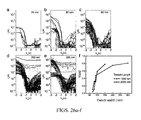
- FIG. 28 is a diagram illustrating random bits devices with local gates according to an embodiment of the present invention.
- the cryptographic keys provided herein are more robust against reverse-engineering and other tactics used to impermissibly obtain the key.
- metallic carbon nanotube interconnects are employed as part of a cryptographic key anti-tampering device.
- the metallic carbon nanotube forms part of a word line (WL) connection to a memory cell—wherein the cryptographic key is stored in the memory cell.
- the metallic carbon nanotube prevents any reverse-engineering to directly access any metal levels below the metallic carbon nanotube.
- the word line signal will pass through higher metal levels and the short metallic carbon nanotube segment, and return to the memory cell. Attempts to reverse engineer by delayering the device will destroy the metallic carbon nanotube interconnect, and thereby the stored key will lose its connection and function.
- FIGS. 1-5 An exemplary process for forming a cryptographic key having a metallic carbon nanotube-based anti-tampering feature according to this exemplary embodiment is described by way of reference to FIGS. 1-5 .
- the process begins with the fabrication of a memory cell.
- the memory cell is a standard memory transistor such as a floating-gate transistor. See FIG. 1 . This, however, is merely an example meant to illustrate the present techniques.
- the anti-tampering features are broadly applicable to any non-volatile memory cell configurations wherein individual memory cells are accessed via a word line and a bit line.
- the instant memory cell could be a floating-gate transistor, a magnetic random access memory (MRAM) magnetic memory cell, a resistive random-access memory (RRAM) cell, a phase change memory (PCM) cell, a flash memory cell, an erasable programmable read only memory (EPROM) cell, etc.
- MRAM magnetic random access memory
- RRAM resistive random-access memory
- PCM phase change memory
- EPROM erasable programmable read only memory
- the carbon nanotube-based anti-tampering feature will be used to form an interconnect between the word line (or higher metal level) and the memory cell. What is important is that this carbon nanotube anti-tampering feature is destroyed (during the above-described delayering process) before the word line can be accessed.
- the example illustrated in the figures uses a standard memory transistor such as a floating-gate transistor which includes a source (S) and a drain (D) interconnected by a channel, and a gate (G) over the channel which serves to regulate electron flow through the channel. Spacers are often used on opposite sides of the gate (G) to offset the gate (G) from the source (S) and the drain (D). See FIG. 1 .
- the present techniques are broadly applicable to any non-volatile memory cell configuration, e.g., floating-gate transistor, MRAM, RRAM, PCM, flash memory, EPROM, etc. wherein the memory cell is accessed via a word line and a bit line.
- MRAM floating-gate transistor
- RRAM resistive RAM
- PCM phase change memory
- flash memory e.g., EPROM, etc.
- the transistor may be fabricated using standard processing techniques including, but not limited to, defining an active area of the memory cell in a wafer, gate (G) material deposition and patterning, spacer formation, source (S) and drain (D) implantation, etc.
- G gate
- S source
- D drain
- the process for fabricating a transistor on a wafer would be apparent to one skilled in the art, and thus is not described further herein. It is noted that for ease and clarity of depiction, the wafer (substrate upon which the memory transistor is constructed) is not shown. However, any suitable semiconductor wafer configuration may be employed including, but not limited to, a bulk semiconductor wafer, a semiconductor-on-insulator (SOI) wafer, etc.
- SOI semiconductor-on-insulator
- conventional key storage technology is employed in the sense that the key is stored in the memory cell (e.g., in this example—in the memory transistor).
- the present techniques introduce a unique metallic carbon nanotube-based anti-reverse engineering feature.
- this metallic carbon nanotube-based anti-reverse engineering feature is destroyed during a delayering process aimed to extract the key, the stored key will lose its connection and function.
- carbon nanotube-based technology is used to physically create the cryptographic key itself, i.e., randomly deposited metallic or semiconducting carbon nanotubes become the key.
- the memory cell is accessed via a word line (WL) and a bit line (BL), wherein an intersection of the word line and the bit line is the address of the memory cell.
- WL word line
- BL bit line
- the word line contacts the gate (G) of the transistor.
- each magnetic memory cell is accessed via a word line and a bit line running above and below (or alternatively below and above) the memory cell. See, for example, U.S. Pat. No. 7,433,225 issued to Daniel C. Worledge, entitled “Scalable magnetic random access memory device,” the contents of which are incorporated by reference as if fully set forth herein.
- MRAM as opposed to a memory transistor would provide the same word line connection to the memory cell (or other higher metal layer) into which the present carbon nanotube interconnect-based anti-tampering feature could be placed.
- the description that follows highlights an implementation involving a memory transistor one skilled in the art could apply this teaching to place the present anti-tampering feature in the metal layers accessing any type of non-volatile memory cell.
- the process for forming the word and bit lines to include the metallic carbon nanotube anti-tampering feature will now be described. Specifically, as shown in FIG. 2 , the next step in the process is to form contacts to the source (S), drain (D), and gate (G). It is notable that in this depiction, the drain (D) contact is not being shown as it would be constructed along with the adjacent memory transistor, however the same process described would be applied to form the drain (D) contact.
- the source (S), drain (D), and gate (G) contacts consist of metal (or other electrically conductive material)-filled vias that connect the memory transistor to a first metal layer (M 1 ).
- the process for forming source (S), drain (D), and gate (G) contacts involves depositing a dielectric material (DE 1 ) (such as silicon dioxide (SiO 2 )) over the memory transistor, patterning vias in the dielectric material (DE 1 ), and then filling the vias with a conductive material such as a metal or metals.
- a simple dotted line is being used to schematically represent the placement of the dielectric material (DE 1 ) with the understanding that the configuration of such a standard interlayer dielectric would be apparent to one skilled in the art.
- a M 1 metal layer is formed contacting the source (S) and gate (G) contacts. See FIG. 3 .
- the corresponding word line (WL) is formed as part of the M 1 metal layer.
- the M 1 metal layer can be formed using a standard damascene metallization process wherein a dielectric material (DE 2 ) (such as SiO 2 ) is first deposited, covering the source (S) and gate (G) contacts.
- a dielectric material such as SiO 2
- a simple dotted line is being used to schematically represent the placement of the dielectric material (DE 2 ) with the understanding that the configuration of such a standard interlayer dielectric would be apparent to one skilled in the art.
- Standard lithography and etching techniques can then be used to pattern the dielectric material (DE 2 ) with the footprint and location of the M 1 metal lines, including the word line (WL).
- the pattern is then filled with a conductive material such as metal(s) (e.g., copper) to form the M 1 metal lines.
- the M 1 -M 2 interconnects are then formed which will serve to interconnect the M 1 metal layer with an M 2 metal layer (see below). See FIG. 4 .
- the M 1 -M 2 interconnects consist of metal (or other electrically conductive material)-filled vias.
- a dielectric material (DE 3 ) such as SiO 2
- vias are patterned in the dielectric material (DE 3 ), and then the vias are filled with a conductive material such as a metal or metals.
- a simple dotted line is being used to schematically represent the placement of the dielectric material (DE 3 ) with the understanding that the configuration of such a standard interlayer dielectric would be apparent to one skilled in the art.
- an M 2 metal layer is formed. See FIG. 5 .
- the corresponding bit line (BL) is formed as part of the M 2 metal layer, as is the metallic carbon nanotube-based anti-tampering feature (see below).
- the M 2 metal layer can be formed using a standard damascene metallization process wherein a dielectric material (DE 4 ) (such as SiO 2 and/or hafnium oxide (HfO 2 )—see below) is first deposited, covering the M 1 -M 2 interconnects.
- a dielectric material such as SiO 2 and/or hafnium oxide (HfO 2 )—see below
- an exemplary process for depositing a metallic carbon nanotube (which serves as the present interconnect/anti-tampering feature) by way of a self-assembly process is provided below whereby a trench is formed in the dielectric (i.e., in this case in the DE 4 dielectric layer) and the carbon nanotube is placed selectively in the trench.
- This exemplary technique is however only one of a number of different possible techniques that may be employed to place the present carbon nanotube-based anti-tampering feature—see below. Standard lithography and etching techniques can then be used to pattern the dielectric material (DE 4 ) with the footprint and location of the M 2 metal lines, including the bit line (BL).
- the pattern is then filled with a conductive material such as metal(s) (e.g., copper) to form the M 2 metal lines.
- a conductive material such as metal(s) (e.g., copper) to form the M 2 metal lines.
- metal(s) e.g., copper
- a trench is formed in the dielectric material (DE 4 ) into which the metallic carbon nanotube is deposited/placed which will serve as an interconnect/anti-tampering feature. It is however noted that any suitable process for placing a carbon nanotube may be used in accordance with the present techniques.
- the word line (WL) is connected directly to the gate (G).
- the metallic carbon nanotube-based anti-tampering feature is inserted between the word line (WL) and the gate (G).
- Carbon nanotubes are small and thus cannot be easily detected without advanced imaging techniques such as a scanning electron microscope (SEM).
- SEM scanning electron microscope
- the carbon nanotube used in this example is a metallic carbon nanotube.
- Carbon nanotubes, as produced, will naturally contain both semiconducting and metallic carbon nanotubes.
- a metallic carbon nanotube is needed.
- Techniques are known in the art for separating metallic from semiconducting carbon nanotubes which may be implemented in accordance with the present techniques. See, for example, Tulevski et al., “High Purity Isolation and Quantification of Semiconducting Carbon Nanotubes via Column Chromatography,” ASC Nano, vol. 7, no. 4, pgs. 2971-2976 (March 2013) (hereinafter “Tulevski”), the contents of which are incorporated by reference as if fully set forth herein. Using the techniques described in Tulevski, sorted samples of metallic carbon nanotubes can be obtained (see, for example, FIG. 1 of Tulevski).
- FIG. 5 represents a single memory bit. Many memory applications employ an array of memory bits oriented along the word and bit lines. As would be apparent to one skilled in the art, the techniques described in conjunction with the description of FIGS. 1-5 above could be implemented in the same manner described to produce an array of interconnected memory bits, such as in FIG. 5A .
- FIG. 5A shows an array of memory bits formed according to the process illustrated in FIGS. 1-5 wherein each of the memory bits has the metallic carbon nanotube-based anti-tampering feature between the word line and the gate.
- FIG. 5A depicts, for illustrative purposes only, two memory bits along a given word line and two memory bits along a given bit line merely to exemplify how the memory bits are configured in an array. As would be apparent to one skilled in the art, more memory bits would likely exist than what is shown.
- metallic carbon nanotube interconnect anti-tampering feature was described above. Now provided is an exemplary technique that might be implemented in accordance with the present techniques to selectively place the present metallic carbon nanotube interconnect within the M 2 metal layer.
- any technique used for the selective placement of a metallic carbon nanotube(s), in a specified position for use as an interconnect may be employed in accordance with the present techniques.
- metallic carbon nanotubes can be simply cast from an aqueous solution (for example using a spin-coating process) to place the present metallic carbon nanotube interconnect.
- a mask may be employed to ensure proper placement.
- chemical self-assembly techniques are used as described, for example, in Park et al. “High-density integration of carbon nanotubes via chemical self-assembly,” Nature Nanotechnology, 7, 787-791 (October 2012) (hereinafter “Park”), the contents of which are incorporated by reference as if fully set forth herein.
- Park selective placement can be achieved based on ion exchange between a functional surface monolayer and surfactant-wrapped carbon nanotubes which are processed in an aqueous solution.
- a surface monolayer is formed from 4-(N-hydroxycarboxamido)-1-methylpyridinium iodide (NMPI) which contains hydroxamic acid end groups that are known to self-assemble on metal oxide surfaces (such as HfO 2 ) but not on SiO 2 .
- NMPI 4-(N-hydroxycarboxamido)-1-methylpyridinium iodide
- the functionalized surface can then be contacted with an aqueous solution of surfactant-wrapped carbon nanotubes whereby the anion of the NMPI is exchanged with the anionic surfactant wrapped around the carbon nanotubes leading to a strong coulombic attraction between the negatively charged surfactant and the positively charged monolayer.
- self-assembly of the carbon nanotubes can be achieved on the HfO 2 surfaces selective to the SiO 2 surfaces.
- a bilayer dielectric is next deposited onto the dielectric material (DE 3 ) covering the M 1 -M 2 interconnects, i.e., the dielectric material DE 4 in this example will be made up a HfO 2 /SiO 2 bilayer. See FIGS. 7 and 8 .
- the first layer of the bilayer dielectric is a HfO 2 layer 702 deposited onto the dielectric material (DE 3 ) covering the M 1 -M 2 interconnects.
- the second layer of the bilayer dielectric is a SiO 2 layer 802 deposited onto the HfO 2 layer 702 .
- the metallic carbon nanotube interconnect is then placed followed by formation of the M 2 metal lines.
- the metallic carbon nanotube interconnect is placed (selectively) within a trench formed in the dielectric.
- standard lithography and etching can be used to form a trench 902 in the SiO 2 layer 802 . See FIG. 9 .
- the trench 902 corresponds to the location of the metallic carbon nanotube interconnect.
- a selective etch process is used to etch the trench 902 through only SiO 2 layer 802 of the bilayer dielectric.
- the result, as shown in FIG. 9 is the exposure of HfO 2 layer 702 within the trench 902 .
- NMPI NMi-silicon
- metal oxide surfaces in this case HfO 2
- SiO 2 metal oxide surfaces
- the NMPI monolayer will form only within the trench 902 . See FIG. 10 .
- An aqueous solution of surfactant-wrapped metallic carbon nanotubes is prepared.
- the carbon nanotubes are wrapped by a surface-active dispersing agent, such as sodium dodecylsulfate (SDS). Wrapping the carbon nanotubes in the surfactant allows the carbon nanotubes to be dispersed in water forming the aqueous solution.
- Column chromatography is then used to isolate the metallic carbon nanotubes according to the process described in Tulevski. Excess SDS can be removed by dialysis to obtain a high carbon nanotube deposition yield.
- the aqueous solution of the surfactant-wrapped metallic carbon nanotubes is then contacted with the NMPI surface. See FIG. 11 .
- the negative iodide ion of the NMPI monolayer is exchanged with the positive sodium ion of the SDS to form sodium iodide, resulting in a strong Coulombic attraction between the positively charged (NMPI) monolayer and the negatively charged surfactant.
- the metallic carbon nanotube(s) will adhere only to the NMPI surface.
- the carbon nanotube deposition on NMPI is facilitated by the attached SDS, as well as being deterred by free SDS surfactant blocking NMPI sites.
- the yield of nanotube placement can be controlled by tuning the concentration of free SDS surfactant, as well as controlling the salt concentration which controls Debye length in the solution as the ionic strength, and/or the dimension of the trench 902 (see below). For instance, by changing the ionic strength by adjusting the salt concentration, one can control the electrostatic interaction in the solution and thereby control the carbon nanotube placement. Tailoring the dimensions of the trenches to control carbon nanotube placement is described below. It is notable that in this case, 100% yield of (metallic carbon nanotubes) in the trenches is desired in this anti-tampering feature embodiment since the carbon nanotubes serve as interconnects.
- the M 2 metal lines can then be formed in contact with the metallic carbon nanotube interconnect and with the underlying M 1 -M 2 interconnects.
- standard lithography and etching can be used to form a pattern 1202 for the M 2 metal layer in the bilayer dielectric. See FIG. 12 .
- the pattern 1202 extends through both the SiO 2 layer 802 and the HfO 2 layer 702 , thus exposing the underlying dielectric material (DE 3 ) and the M 1 -M 2 interconnects. This will enable the M 2 metal lines (which will be formed in the trenches—see below) to contact the M 1 -M 2 interconnects.
- the pattern 1202 is then filled with a conductive material such as a metal (e.g., copper)—forming the M 2 metal lines. See FIG. 13 . Excess metal can be removed using a mechanical etching process such as grinding.
- a conductive material such as a metal (e.g., copper)—forming the M 2 metal lines. See FIG. 13 .
- Excess metal can be removed using a mechanical etching process such as grinding.
- a metallic carbon nanotube interconnect may instead (or in addition to) be placed in one or more higher metal levels (so long as the carbon nanotube anti-tampering feature is destroyed (during reverse-engineering efforts) before the word line is revealed—thereby removing any connection between the memory cell and the word line. Redundancy can increase the degree of protection.
- the same process described above for selectively placing metallic carbon nanotube(s) can be applied to any layer in the circuit.
- a (HfO 2 /SiO 2 ) bilayer dielectric can be employed for any of the dielectric layers (DE 1 - 4 ) thus enabling selective carbon nanotube placement via the self-assembly process in Park. See above.
- the key is generated during fabrication of the circuit by depositing randomly either metallic or semiconducting carbon nanotubes.
- the randomness of the deposited carbon nanotubes is the “key” itself.
- the key is generated during fabrication of the circuit it can be read from the chip and stored by the server.
- conventional key storage techniques are employed wherein the key is stored in a memory cell.
- the (metallic) carbon nanotube interconnects in that case are used as an anti-tampering feature such that when delayering is used to reverse-engineer the circuit the metallic carbon nanotube interconnect is destroyed and with it the stored key gate connection (and function).
- each bit in a carbon nanotube cryptographic key can be metallic, semiconducting, or no-tube. This process provides a low-cost and hard-to-forge approach for implementing physical security primitives.
- Pappu a unique speckle pattern can be generated when shining a laser through an optical epoxy token with inhomogeneous scatters.
- the format of the physical unclonable function (PUF) was later expanded from non-electronic devices to integrated circuit-based electronic devices. See, for example, Gassend et al., “Silicon Physical Random Functions,” Proceedings of the 9 th ACM conference on Computer and communications security CCS '02, pgs.
- mismatches arising from these stochastic atomic variations are likely to follow a Gaussian distribution, in which a large portion of the mismatches are very close to zero mean.
- PUFs based on these small mismatches can be easily disturbed by noises and environmental factors which can lead to large bit error rates in the output.
- pre-processing, to rule out devices with small mismatches or post-processing to reduce the bit error rate is required in silicon PUFs.
- ring oscillator or arbiter PUFs are based on mismatches of two or multiple delay chains, which are subject to the averaging effect of mismatches in multiple stages. See, for example, S. S.
- CMOS complementary metal-oxide-semiconductor
- a non-volatile, low-cost PUF also referred to herein as a “physically unclonable function” which is based on self-assembled carbon nanotubes.
- the present physically unclonable cryptographic key includes an array of memory cells. Each of the memory cells represents a single bit.
- memory cell and “bit” are used interchangeably herein.
- each bit includes a selecting field effect transistor (FET) (or simply “selecting transistor”).
- FET field effect transistor
- selecting transistor For smaller arrays a selecting transistor may not be required, and such an example is provided below. In most cases however, with larger arrays selecting transistors are needed to access specific bits.
- FET field effect transistor
- FIGS. 14-18 An exemplary methodology for fabricating the bits in the array is now provided by way of reference to FIGS. 14-18 . What is shown and described in the following example makes reference to a single given one of the bits, with the understanding that the same process applies to producing the multiple bits that form the array (see, for example, FIG. 18A —described below).
- the bits in the array are identical to one another except for the carbon nanotube component which, due to the randomness of the self assembly process, is metallic and/or semiconducting.
- the process begins by forming the selecting FET (one for each of the memory cells). See FIG. 14 .
- a standard FET includes a source (S) and a drain (D) interconnected by a channel, and a gate (G) over the channel which serves to regulate electron flow through the channel. Spacers are often used on opposite sides of the gate (G) to offset the gate (G) from the source (S) and the drain (D) (see FIG. 14 ).
- the selecting FET may be fabricated using standard processing techniques including, but not limited to, defining an active area of the memory cell in a wafer, gate (G) material deposition and patterning, spacer formation, source (S) and drain (D) implantation, etc.
- any suitable semiconductor wafer configuration may be employed including, but not limited to, a bulk semiconductor wafer, a semiconductor-on-insulator (SOI) wafer, etc.
- Each bit is accessed via a word line (WL) and a bit line (BL), wherein an intersection of the word line and the bit line is the address of the bit.
- the word line contacts the gate (G) of the memory cell and the bit line contacts the source (S)/drain (D).
- G gate
- S source
- D source
- a carbon nanotube(s) is inserted in the bit line connection to the source/drain via the above-described self-assembly process which is randomly metallic or semiconducting.
- some bits may receive no carbon nanotube at all, thus adding to the randomness of the key generation process.
- the process for forming the word and bit lines and the (metallic or semiconducting) carbon nanotube key will now be described. Specifically, as shown in FIG. 15 , the next step in the process is to form contacts to the source (S), drain (D), and gate (G). It is notable that in this depiction, the drain (D) contact is not being shown as it would be constructed along with the adjacent bit, however the same process described would be applied to form the drain (D) contact.
- the source (S), drain (D), and gate (G) contacts consist of metal (or other electrically conductive material)-filled vias that connect the selecting transistor to a first metal layer (M 1 ).
- the process for forming source (S), drain (D), and gate (G) contacts involves depositing a dielectric material (DE 1 ) (such as SiO 2 ) over the selecting transistor, patterning vias in the dielectric material (DE 1 ), and then filling the vias with a conductive material such as a metal or metals.
- a simple dotted line is being used to schematically represent the placement of the dielectric material (DE 1 ) with the understanding that the configuration of such a standard interlayer dielectric would be apparent to one skilled in the art.
- an M 1 metal layer is formed contacting the source (S) and gate (G) contacts. See FIG. 16 .
- the corresponding word line (WL) is formed as part of the M 1 metal layer.
- the M 1 metal layer can be formed using a standard damascene metallization process wherein a dielectric material (DE 2 ) (such as SiO 2 ) is first deposited, covering the source (S) and gate (G) contacts.
- a dielectric material such as SiO 2
- a simple dotted line is being used to schematically represent the placement of the dielectric material (DE 2 ) with the understanding that the configuration of such a standard interlayer dielectric would be apparent to one skilled in the art.
- Standard lithography and etching techniques can then be used to pattern the dielectric material (DE 2 ) with the footprint and location of the M 1 metal lines, including the word line (WL).
- the pattern is then filled with a conductive material such as metal(s) (e.g., copper) to form the M 1 metal lines.
- the M 1 -M 2 interconnects are then formed which will serve to interconnect the M 1 metal layer with an M 2 metal layer (see below). See FIG. 17 .
- the M 1 -M 2 interconnects consist of metal (or other electrically conductive material)-filled vias.
- a dielectric material (DE 3 ) such as SiO 2
- vias are patterned in the dielectric material (DE 3 ), and then the vias are filled with a conductive material such as a metal or metals.
- a simple dotted line is being used to schematically represent the placement of the dielectric material (DE 3 ) with the understanding that the configuration of such a standard interlayer dielectric would be apparent to one skilled in the art.
- the M 2 metal layer is formed. See FIG. 18 .
- the M 2 metal layer can be formed using a standard damascene metallization process wherein a dielectric material (DE 4 ) is first deposited, covering the M 1 -M 2 interconnects.
- DE 4 dielectric material
- the M 1 metal layer is separated from the M 2 metal layer by dielectric, namely the DE 3 and DE 4 dielectric layers. It is in the DE 4 dielectric layer which a trench is formed to place a (randomly) metallic or semiconducting carbon nanotube which will serve to connect the bit line with the source of the selecting transistor—see below.
- Standard lithography and etching techniques can then be used to pattern the dielectric material (DE 4 ) with the footprint and location of the M 2 metal lines, including the bit line (BL).
- the pattern is then filled with a conductive material such as metal(s) (e.g., copper) to form the M 2 metal lines.
- a carbon nanotube(s) is/are placed in the M 2 metal layer between the bit line and the source of the selecting transistor. Due to the self-assembly process employed, the carbon nanotube(s) is/are randomly metallic and/or semiconducting. As will be described in detail below, this randomness throughout the array constitutes the key.
- a trench is formed in the DE 4 dielectric material.
- the DE 4 dielectric material might be configured as a bilayer with a layer of SiO 2 over a layer of HfO 2 . Accordingly, the trench can be formed in the SiO 2 top layer exposing the underlying HfO 2 .
- a monolayer of NMPI may then be formed on the exposed HfO 2 via a self-assembly process.
- An aqueous solution of SDS-wrapped carbon nanotubes is prepared. Excess SDS can be removed by dialysis to obtain a high carbon nanotube deposition yield. Based on the different chiralities of the carbon nanotubes as synthesized, the solution will contain both metallic and semiconducting carbon nanotubes. In this case, it is desirable to have both metallic and semiconducting carbon nanotubes since the randomness of placing either a metallic or semiconducting carbon nanotube in a given bit based on the self-assembly process contributes to the ‘unclonability’ of the key.
- the carbon nanotubes will self-assemble in the trenches (throughout the array) due to the strong Coulombic attraction between the positively charged (NMPI) monolayer and the negatively charged SDS (see above).
- the randomness of the (metallic and/or semiconducting) carbon nanotube placement makes reproducing the key impossible (i.e., unclonable).
- the key can be read out once and saved to the server.
- FIG. 18 is a diagram illustrating an array of bits formed according to the process illustrated in FIGS. 14-18 wherein each of the bits randomly has either a metallic or a semiconducting carbon nanotube between the bit line and the source/drain.
- FIG. 18A depicts, for illustrative purposes only, two bits along a given word line and two bits along a given bit line merely to exemplify how the memory bits are configured in an array. As would be apparent to one skilled in the art, more bits would likely exist than what is shown.
- FIG. 19 provides an exemplary methodology 1900 for processing the present carbon nanotube-based physically unclonable cryptographic key.
- the cryptographic key is created (according to the process illustrated in FIGS. 14-18 and described above) as an array of bits, each bit containing a self-assembled carbon nanotube that is randomly either metallic (M) or semiconducting (S) (i.e., CNT/CMOS array).
- M metallic
- S semiconducting
- the carbon nanotube in each bit is illustrated by a box labeled “CNT.”
- the key is read from the chip. In the example depicted in FIG. 19 , a plurality of chips is being produced on a given wafer.
- the regions or spaces between chips on a wafer are commonly known as the kerf.
- readout pads are provided on the kerf for each of the bits.
- a wafer probe can then be used in step 1904 to read out the key (i.e., the bit output states—see below) from each of the pads.
- the ‘key’ will be whether the bit(s) has/have a metallic (M) or semiconducting (S) carbon nanotube which occurs randomly based on the above-described process.
- the array of bits generates a unique combination of metallic (M) or semiconducting (S) carbon nanotube-containing bits.
- a third optional scenario where there is no carbon nanotube present in a bit. That condition is referred to herein as an open bit—see below.
- the readout pads can optionally be connected to the bits via electronic fuses (e-fuses).
- e-fuses electronic fuses
- the e-fuses can be blown which means that the key (the carbon nanotube array information) cannot be directly accessed anymore—the output of the key array can only enter the on-die encryption circuit.
- step 1906 the key readout from the chip is stored to the server.
- the key consists of a unique combination of (randomly, generated) metallic (M) and semiconducting (S) carbon nanotube-containing bits.
- M metallic
- S semiconducting
- the key stored in the server can be used to authenticate the chip.
- the key cannot be reproduced (reverse-engineered) due to the random self-assembly process used to place the carbon nanotubes.
- FIG. 20 a is a diagram illustrating information read out (as per methodology 1900 ) from an exemplary carbon nanotube array cryptographic key according to the present techniques. Specifically, in FIG. 20 a gate voltage V g is plotted on the x-axis and drain current I D is plotted on the y-axis. FIG. 20 a illustrates the three scenarios randomly possible for any given bit in the array, a) the bit contains no carbon nanotube—i.e., it is an open bit, b) the bit contains a semiconducting (S) carbon nanotube, and c) the bit contains a metallic carbon nanotube. The output in the case of an open bit simply represents noise.
- S semiconducting
- FIG. 20 b is a diagram illustrating the carbon nanotube bit output states for each of the three scenarios a) open bit, b) semiconducting carbon nanotube, and c) metallic carbon nanotube.
- the dimensions of the trenches can be varied to further increase the randomness of the key.
- a trench width can be chosen (i.e., the same width will be used for all the trenches on a given chip) that provides about a 50% chance that a carbon nanotube will be deposited inside the trench. Since as will be described in detail this placement process is based on both attractive and repulsive forces acting on the carbon nanotube, the placement process is also random (one cannot control which trenches will eventually have a carbon nanotube) and thus tailoring the trench width in this manner can create additional randomness.
- reducing the trench width increases the interaction between the SiO 2 sidewalls of the trench and the surfactant-wrapped carbon nanotubes, both of which are negatively charged—generating repulsive forces. Reducing the trench width can thus lead to the absence of carbon nanotubes in one or more of the bits. See, for example, FIG. 21 which illustrates the concept of trench dimension (length/width) and attractive/repulsive forces acting on the negatively charged (SDS-wrapped) carbon nanotubes (CNT-SDS) by the positively charged NMPI and the negatively charged SiO 2 . It is notable that, in accordance with the present techniques, the patterned SiO 2 /HfO 2 surface can be configured as shown here in FIG.
- the width of patterned HfO 2 trenches can be varied, if so desired, to achieve random placement of the carbon nanotubes.
- This concept can be illustrated by the following non-limiting example—by reducing the trench width from about 300 nanometers (nm) to about 70 nm, the repulsive force between negatively charged SiO 2 sidewall and negatively charged SDS wrapping around the carbon nanotube (SDS-CNT) becomes more prominent compared to the attractive force between the NMPI monolayer and the SDS-CNT. By carefully designing the trench dimension, this competition between the attractive force and the repulsive force can lead to highly random CNT placement inside the trench, see FIG. 21 .
- the trenches are configured to have a height which is relatively larger than the dimension of the carbon nanotubes—for example a height of from about 5 nm to about 10 nm, and ranges therebetween, e.g., about 7 nm. As shown in FIG. 21 , the height of the trench is measured from the surface of the HfO 2 to the top surface of the SiO 2 (the NMPI is a monolayer and has almost no thickness).
- the result of the present self-assembly process is a random array of carbon nanotubes.
- FIG. 21 is a simplified version of the array which in production would include word and bit lines and preferably a selecting transistor for each bit. See, for example, FIGS. 14-18 , described above.
- Measurements from the random carbon nanotube array may be obtained using a two-dimensional (2D) wiring structure as shown in FIG. 22 .
- 2D two-dimensional
- FIG. 22 shows how the connected (black) and disconnected (white) bits are distributed in a 5 ⁇ 5 two-dimensional array.
- the array size can be significantly expanded when incorporating row and column multiplexers commonly used in memory arrays, thus more random bits can be generated for higher security requirements.
- Simulation a simulation of the interaction between SDS-wrapped carbon nanotubes and the charged surface was carried out using COMSOL Multiphysics® Modeling Software based on finite element methods.
- the structure is shown in FIGS. 23 a and 23 b , in which the out-of-plane length of the carbon nanotube and pattern is 500 nm.
- Surface charge density of the SDS-wrapped carbon nanotube, SiO 2 and NMPI on HfO 2 used in the simulation is ⁇ 0.05, ⁇ 0.49 and 0.1 coulomb per square centimeter (C/cm 2 ), respectively.
- the salt concentration is 0.1 millimolar (mM).
- FIGS. 23 a - f illustrate the surface charge effects of a patterned SiO 2 and NMPI (monolayer) substrate surface on SDS-wrapped carbon nanotube assembly.
- FIG. 23 a shows the surface potential near a patterned SiO 2 and NMPI (monolayer) substrate surface with a trench width/barrier width of 30 nanometers (nm)/30 nm.
- FIG. 23 b shows the surface potential near the patterned substrate surface with a trench width/barrier width of 80 nm/80 nm.
- FIG. 23 c illustrates an x-component electromagnetic force profile as a function of carbon nanotube position moving toward the trench surface with the geometry of FIG. 23 a and FIG. 23 b .
- FIG. 23 a shows the surface potential near a patterned SiO 2 and NMPI (monolayer) substrate surface with a trench width/barrier width of 30 nanometers (nm)/30 nm.
- FIG. 23 b shows the surface potential near the
- FIG. 23 d shows the surface potential with off-centered carbon nanotubes with trench width/barrier width of 30 nm/30 nm.
- FIG. 23 e illustrates an x-component electromagnetic force profile as a function of carbon nanotube position moving in parallel with the surface.
- FIG. 23 f illustrates a y-component electromagnetic force profile as a function of carbon nanotube position moving in parallel with the surface.
- FIG. 23 a and FIG. 23 b have the same coordinate axis and scale (scale bar: 30 nm). The shaded bar shown to the right of FIG. 23 a applies to FIG. 23 a , FIG. 23 b , and FIG. 23 d.
- FIG. 24 is a diagram illustrating the combination number of 2-state bits in log e scale as a function of total bits number and the yield of connected bits.
- EDLs Electrical double layers
- the carbon nanotube has to be within 20 nm from the HfO 2 surface to be attracted toward the surface, as also shown in FIG. 23 c .
- the carbon nanotube always experiences overall attractive force from surfaces based on the similar simulation shown in FIG. 23 c .
- diffusion of the SDS-wrapped carbon nanotube from bulk solution toward the surface is energetically unfavorable for the geometry with a small trench width because of net repulsive force from the patterned surface.
- the EDLs of the carbon nanotube, SiO 2 and monolayer are significantly overlapped, indicating a strong interaction. This interaction leads to a lateral force ( FIG. 23 e ) tending to move the carbon nanotube to the center of the trench and this force decays as the separation from the surface increases.
- the carbon nanotube experiences a vertical force with strength and polarity strongly depending on the carbon nanotube's position.
- the width of this placement window can be well controlled by the trench width, providing the design parameter to control CNT placement yield (to ⁇ 50% for the highest randomness).
- each of the bits in the array has a selecting FET.
- the FETs enable accurate selection of any given bit in the array. If the array is small enough, however, it is possible to construct bits without a selecting FET.
- FIGS. 25 a - c An example of a simplified small array of bits that do not include selecting FETs is shown in FIGS. 25 a - c . In this case, bits are accessed by selecting the word and bit lines in the array that intersect at the corresponding bit. Namely, FIG. 25 a demonstrates the fabrication of this simplified two-dimensional array of self-assembled carbon nanotube devices and FIG. 25 b shows a scanning electron microscopy (SEM) image of a 5 ⁇ 5 carbon nanotube crossbar structure.
- SEM scanning electron microscopy
- this two-dimensional array of carbon nanotube devices is fabricated by the following process.
- Carbon nanotubes are first deposited using the above-described chemical self-assembly method.
- trenches with different dimensions are patterned on an HfO 2 blanket film, followed by 7 nm thick SiO 2 evaporation and a lift-off process.
- Electron-beam lithography is used to define all the patterns mentioned here, either in poly(methyl methacrylate) (PMMA) or hydrogen silsesquioxane (HSQ).
- PMMA poly(methyl methacrylate)
- HSQ hydrogen silsesquioxane
- the patterned substrate is then immersed in a 3.5 mM solution of NMPI (3:1 ethanol/water) for 1 hour, followed by rinsing with ethanol to complete the NMPI monolayer coating.
- NMPI 3:1 ethanol/water
- Several drops of nanotube solution are put down on top of the substrate and covered with a thin glass slide.
- DI deionized
- the substrate is rinsed with deionized (DI) water for 30 seconds and sonicated in DI water for 1 minute.
- DI deionized
- the carbon nanotubes can be patterned by reactive ion etch (RIE) in oxygen using double layers of PMMA and HSQ as a etch mask.
- RIE reactive ion etch
- the HSQ layer is removed by lifting off underlying PMMA layer in hot acetone.
- the substrate is then thermal annealed at 400 degrees Celsius (° C.) in vacuum of 1 ⁇ 10 ⁇ 7 torr to drive off the monolayer and SDS to recover the electrical properties of CNTs.
- the first metal layer 0.5 nm titanium (Ti)/20 nm palladium (Pd)/10 nm gold (Au)
- 2% HSQ is patterned as an insulating layer between two metal layers.
- the second metal layer 0.5 nm Ti/20 nm Pd/30 nm Au
- the completed device can be annealed at 150° C. in hexamethyldisilazane (HMDS) ambient for 40 minutes to improve device performance.
- HMDS hexamethyldisilazane
- FIG. 25 c presents an enlarged view of the region from FIG. 25 b within the hatched box, which shows both bit “ 0 ” (without a carbon nanotube connection—on the left) and bit “ 1 ” (with a carbon nanotube connection—on the right). Due to the extremely small body size of carbon nanotubes, the area consumption of the carbon nanotube device is only limited by metal leads and contacts. This two-dimensional array structure enables high-density integration of carbon nanotubes by largely reducing lead and pad numbers. All of the carbon nanotubes in different trench widths were electrically examined in order to analyze the width dependent self-assembly behavior.
- FIGS. 26 a - e show the semilogarithmic current-voltage (I-V) curves from the measurement of CNT arrays with different trench widths (i.e., 70 nm, 80 nm, 90 nm, 200 nm, and 300 nm, respectively) which illustrates the trench-width dependent self-assembly behavior of the carbon nanotubes.
- FIG. 26 f shows quantitative yield of connected bits corresponding to FIGS. 26 a - e . The yield scales with the trench width for both 1500 nm and 2000 nm trench lengths, with a transition from 70-100 nm and saturation beyond 150 nm, which is attributed to the abovementioned competition between the attractive force and the repelling force.
- the trench width of 80 nm is chosen for its ability to realize a connection yield close to 50%.
- FIG. 27 a shows the I-V curves of 1200 devices, all with 80 nm trench width.
- white dots are connecting devices and black dots are open devices.
- a threshold current of 2 nanoamperes (nA) at a gate voltage of ⁇ 3 V was set to determine the connection type of each bit, and a 48 ⁇ 25 2-state random bits map is constructed as shown in FIG. 27 b .
- the Hamming distance is calculated by comparing bit-to-bit difference between two keys.
- the distribution of the normalized Hamming distance of 48-bit keys is found to be centered at 0.5 with a boundary of 0.25 to 0.65, as shown in FIG. 27 c . That means any two different keys generated based on this technology differ in at least 12 bits which is 25% of the 48-bit key.
- Synthesized carbon nanotubes naturally contain both semiconducting and metallic nanotubes, which is detrimental to electronic applications but beneficial to cryptographic keys application.
- an additional threshold current of 10 nA at gate voltage of 0 V, one is able to discriminate between switching and non-switching devices among those connected devices.
- 2-state random bits can thus be upgraded to 3-state random bits ( FIG. 27 d ), which is not available in most of the programmable devices.
- white dots are semiconducting devices
- black dots are open devices
- textured dots are non-switching devices.
- the number of possible combinations in 3-state bits (C 3 ) is the number of possible combinations in 2-state bits C 2 (n,m) times C(m,l) where n is the total device number, m is the connected device number, and l is the number of semiconducting devices out of m.
- a simplified formula is then obtained for ln(C 2 (n,m)C(m,l)) as ln(C 2 (n,m)C(m,l)) ⁇ n( ⁇ ( ⁇ )+ ⁇ ( ⁇ )), where ⁇ and ⁇ are connection yield and semiconducting purity respectively (see above).
- the carbon nanotube key possesses physical unclonability originated from the randomness of nanoscale diffusion and drift process. Even knowing the same fabrication process, it is impossible to clone the same carbon nanotube key.
- Optical methods do not have enough resolution to detect the presence of a single nanotube in the trench. Electron microscope imaging requires chip reverse-engineering process, which can easily destroy the nanotube. Attacks by electrical measurement are possible only if knowing the lead layout.
- utilizing the switching behavior of semiconducting nanotubes by incorporating local gates as additional inputs makes the already difficult process even more daunting. As shown in FIG. 28 , the designation of local gates affects the local response of semiconducting carbon nanotubes, thus much more complicated input-output pairs can be realized in this design. Adding more freedom by mixing gates with other inputs makes the measurement more difficult without knowing the layout of local gates.
Landscapes
- Engineering & Computer Science (AREA)
- Computer Security & Cryptography (AREA)
- Computer Networks & Wireless Communication (AREA)
- Signal Processing (AREA)
- Physics & Mathematics (AREA)
- General Physics & Mathematics (AREA)
- Theoretical Computer Science (AREA)
- Semiconductor Memories (AREA)
Abstract
Description
ln(n!)≈n ln(n)−n (2)
is applied, and it is assumed that m=αnα∈(0,1]. The simplified form of the combination equation can be represented by:
ln(C 2(n,m))≈−n[(1−α)ln(1−α)+α ln(α)]≡−nγ(α). (3)
By taking a derivative of function γ(α), the minimum value of γ(α)=−0.6931 can be calculated when α=0.5. And the function ln C2(n,m) is symmetric about axis of α=0.5, as shown in
−∈0∇·[∈(x)∇Ψ(x)]=ρ(x)=e 0 N AΣi=1 N
wherein, Ψ(x) is the electric potential, ρ(x) is the net charge density, ∈0 is the vacuum permittivity and ∈(x) is the dielectric constant of the solution. ci(x) and Zi denote the molar concentration and valence of the ith ionic species respectively.
J i(x)=c i(x)ν(x)−D i ∇c i(x)−μi c i(x)∇Ψ(x). (5)
The diffusion coefficient Di is related to the mobility μi via Einstein relation, μi=Zie0Di/KBT. ν(x) is the velocity field of the fluid. The equation is solved under steady state, where ∇·Ji(x)=0.
Claims (8)
Priority Applications (1)
| Application Number | Priority Date | Filing Date | Title |
|---|---|---|---|
| US14/749,092 US9787473B2 (en) | 2014-12-30 | 2015-06-24 | Carbon nanotube array for cryptographic key generation and protection |
Applications Claiming Priority (2)
| Application Number | Priority Date | Filing Date | Title |
|---|---|---|---|
| US14/586,103 US9660806B2 (en) | 2014-12-30 | 2014-12-30 | Carbon nanotube array for cryptographic key generation and protection |
| US14/749,092 US9787473B2 (en) | 2014-12-30 | 2015-06-24 | Carbon nanotube array for cryptographic key generation and protection |
Related Parent Applications (1)
| Application Number | Title | Priority Date | Filing Date |
|---|---|---|---|
| US14/586,103 Continuation US9660806B2 (en) | 2014-12-30 | 2014-12-30 | Carbon nanotube array for cryptographic key generation and protection |
Publications (2)
| Publication Number | Publication Date |
|---|---|
| US20170063543A1 US20170063543A1 (en) | 2017-03-02 |
| US9787473B2 true US9787473B2 (en) | 2017-10-10 |
Family
ID=56165588
Family Applications (2)
| Application Number | Title | Priority Date | Filing Date |
|---|---|---|---|
| US14/586,103 Expired - Fee Related US9660806B2 (en) | 2014-12-30 | 2014-12-30 | Carbon nanotube array for cryptographic key generation and protection |
| US14/749,092 Expired - Fee Related US9787473B2 (en) | 2014-12-30 | 2015-06-24 | Carbon nanotube array for cryptographic key generation and protection |
Family Applications Before (1)
| Application Number | Title | Priority Date | Filing Date |
|---|---|---|---|
| US14/586,103 Expired - Fee Related US9660806B2 (en) | 2014-12-30 | 2014-12-30 | Carbon nanotube array for cryptographic key generation and protection |
Country Status (1)
| Country | Link |
|---|---|
| US (2) | US9660806B2 (en) |
Families Citing this family (14)
| Publication number | Priority date | Publication date | Assignee | Title |
|---|---|---|---|---|
| US20170077046A1 (en) * | 2015-09-11 | 2017-03-16 | The Regents Of The University Of California | Physical unclonable functions through locally enhanced defectivity |
| US10665799B2 (en) * | 2016-07-14 | 2020-05-26 | International Business Machines Corporation | N-type end-bonded metal contacts for carbon nanotube transistors |
| US10665798B2 (en) | 2016-07-14 | 2020-05-26 | International Business Machines Corporation | Carbon nanotube transistor and logic with end-bonded metal contacts |
| US10225082B2 (en) * | 2016-07-26 | 2019-03-05 | International Business Machines Corporation | Carbon nanotube physical entropy source |
| US10318748B2 (en) * | 2016-09-30 | 2019-06-11 | Intel Corporation | Techniques to protect fuses against non-destructive attacks |
| US10209186B2 (en) * | 2017-01-03 | 2019-02-19 | International Business Machines Corporation | Chemical sensing based on plasmon resonance in carbon nanotubes |
| US10546303B2 (en) | 2017-03-21 | 2020-01-28 | International Business Machines Corporation | Optically visible carbon nanotube with nanocrystals decoration as unique ID |
| US10777265B2 (en) | 2017-11-13 | 2020-09-15 | International Business Machines Corporation | Enhanced FDSOI physically unclonable function |
| EP3550475A1 (en) | 2018-04-06 | 2019-10-09 | Fraunhofer-Gesellschaft zur Förderung der angewandten Forschung e.V. | Puf-film and method for producing the same |
| EP3550623B1 (en) | 2018-04-06 | 2020-07-29 | Fraunhofer-Gesellschaft zur Förderung der angewandten Forschung e.V. | Puf-film and method for producing the same |
| EP3550466B1 (en) * | 2018-04-06 | 2023-08-02 | Fraunhofer-Gesellschaft zur Förderung der angewandten Forschung e.V. | Puf-film and method for producing the same |
| KR102909675B1 (en) * | 2020-05-19 | 2026-01-07 | 삼성전자주식회사 | A non volatile memory device storing a public key and a secret key, an electronic device comprising the same and a service provider |
| CN115065489B (en) * | 2022-08-19 | 2022-11-08 | 北京高科芯联信息科技有限公司 | Safety information generation method and system based on carbon nano tube and electronic equipment |
| US12537699B1 (en) * | 2024-12-12 | 2026-01-27 | Crypto Quantique Limited | Reconfigurable, high stability gate-tunneling physical unclonable function |
Citations (26)
| Publication number | Priority date | Publication date | Assignee | Title |
|---|---|---|---|---|
| US20060064587A1 (en) * | 2004-09-20 | 2006-03-23 | David Braverman | User activated authentication system |
| US20060255414A1 (en) * | 2005-05-16 | 2006-11-16 | Joerg Appenzeller | Method and apparatus for fabricating a carbon nanotube transistor having unipolar characteristics |
| US20070114613A1 (en) * | 2005-11-23 | 2007-05-24 | Lsi Logic Corporation | Programmable nanotube interconnect |
| US7301191B1 (en) * | 2004-09-16 | 2007-11-27 | Atomate Corporation | Fabricating carbon nanotube transistor devices |
| US20080012047A1 (en) * | 2005-05-09 | 2008-01-17 | Nantero, Inc. | Two-terminal nanotube devices and systems and methods of making same |
| US7433225B2 (en) | 2006-07-06 | 2008-10-07 | International Business Machines Corporation | Scalable magnetic random access memory device |
| US20090213649A1 (en) * | 2002-08-29 | 2009-08-27 | Renesas Technology Corp. | Semiconductor processing device and IC card |
| US20100050901A1 (en) | 2008-09-04 | 2010-03-04 | Biris Alexandru S | Multi-level anticounterfeit, security and detection taggant |
| US20100149895A1 (en) * | 2008-12-13 | 2010-06-17 | Juhan Kim | High speed carbon nanotube memory |
| US20100295025A1 (en) * | 2008-01-11 | 2010-11-25 | International Business Machines Corporation | Carbon nanotube based integrated semiconductor circuit |
| US20120068326A1 (en) * | 2010-09-17 | 2012-03-22 | Endicott Interconnect Technologies, Inc. | Anti-tamper microchip package based on thermal nanofluids or fluids |
| US8189419B2 (en) | 2009-07-06 | 2012-05-29 | International Business Machines Corporation | Apparatus for nonvolatile multi-programmable electronic fuse system |
| US20120183135A1 (en) | 2011-01-19 | 2012-07-19 | Verayo, Inc. | Reliable puf value generation by pattern matching |
| US8379856B2 (en) | 2009-06-17 | 2013-02-19 | Empire Technology Development Llc | Hardware based cryptography |
| US20130126830A1 (en) * | 2011-11-23 | 2013-05-23 | International Business Machines Corporation | Transistor employing vertically stacked self-aligned carbon nanotubes |
| US20130210211A1 (en) * | 2011-08-15 | 2013-08-15 | Lidia Vereen | Vertical Cross-Point Memory Arrays |
| US20130232587A1 (en) * | 2012-03-01 | 2013-09-05 | International Business Machines Corporation | Implementing carbon nanotube based sensors for cryptographic applications |
| US8592955B2 (en) | 2011-04-29 | 2013-11-26 | International Business Machines Corporation | Accurate deposition of nano-objects on a surface |
| US8766258B1 (en) | 2012-12-12 | 2014-07-01 | International Business Machines Corporation | Authentication using graphene based devices as physical unclonable functions |
| US20140312248A1 (en) * | 2013-04-23 | 2014-10-23 | Lockheed Martin Corporation | Articles containing non-visible identifying marks formed from nanomaterials and methods utilizing the same |
| US20140364574A1 (en) * | 2013-06-07 | 2014-12-11 | International Business Machines Corporation | Surface-Selective Carbon Nanotube Deposition via Polymer-Mediated Assembly |
| US20150221884A1 (en) * | 2014-01-31 | 2015-08-06 | International Business Machines Corporation | Carbon nanotube transistor having extended contacts |
| US20150235053A1 (en) * | 2012-05-04 | 2015-08-20 | Heon Soo LEE | System on chip, method of operating the same, and devices including the system on chip |
| US9190134B2 (en) * | 2009-04-08 | 2015-11-17 | Sandisk 3D Llc | Three-dimensional array of re-programmable non-volatile memory elements having vertical bit lines and a single-sided word line architecture |
| US20160016801A1 (en) * | 2013-03-05 | 2016-01-21 | Prolume, Ltd. | Self Assembling Beta-Barrel Proteins Position Nanotubes |
| US20160087232A1 (en) * | 2014-01-08 | 2016-03-24 | International Business Machines Corporation | Semiconductor device with ballistic gate length structure |
-
2014
- 2014-12-30 US US14/586,103 patent/US9660806B2/en not_active Expired - Fee Related
-
2015
- 2015-06-24 US US14/749,092 patent/US9787473B2/en not_active Expired - Fee Related
Patent Citations (27)
| Publication number | Priority date | Publication date | Assignee | Title |
|---|---|---|---|---|
| US20090213649A1 (en) * | 2002-08-29 | 2009-08-27 | Renesas Technology Corp. | Semiconductor processing device and IC card |
| US7301191B1 (en) * | 2004-09-16 | 2007-11-27 | Atomate Corporation | Fabricating carbon nanotube transistor devices |
| US20100171099A1 (en) * | 2004-09-16 | 2010-07-08 | Atomate Corporation | Carbon Nanotube Transistor Structure |
| US20060064587A1 (en) * | 2004-09-20 | 2006-03-23 | David Braverman | User activated authentication system |
| US20080012047A1 (en) * | 2005-05-09 | 2008-01-17 | Nantero, Inc. | Two-terminal nanotube devices and systems and methods of making same |
| US20060255414A1 (en) * | 2005-05-16 | 2006-11-16 | Joerg Appenzeller | Method and apparatus for fabricating a carbon nanotube transistor having unipolar characteristics |
| US20070114613A1 (en) * | 2005-11-23 | 2007-05-24 | Lsi Logic Corporation | Programmable nanotube interconnect |
| US7433225B2 (en) | 2006-07-06 | 2008-10-07 | International Business Machines Corporation | Scalable magnetic random access memory device |
| US20100295025A1 (en) * | 2008-01-11 | 2010-11-25 | International Business Machines Corporation | Carbon nanotube based integrated semiconductor circuit |
| US20100050901A1 (en) | 2008-09-04 | 2010-03-04 | Biris Alexandru S | Multi-level anticounterfeit, security and detection taggant |
| US20100149895A1 (en) * | 2008-12-13 | 2010-06-17 | Juhan Kim | High speed carbon nanotube memory |
| US9190134B2 (en) * | 2009-04-08 | 2015-11-17 | Sandisk 3D Llc | Three-dimensional array of re-programmable non-volatile memory elements having vertical bit lines and a single-sided word line architecture |
| US8379856B2 (en) | 2009-06-17 | 2013-02-19 | Empire Technology Development Llc | Hardware based cryptography |
| US8189419B2 (en) | 2009-07-06 | 2012-05-29 | International Business Machines Corporation | Apparatus for nonvolatile multi-programmable electronic fuse system |
| US20120068326A1 (en) * | 2010-09-17 | 2012-03-22 | Endicott Interconnect Technologies, Inc. | Anti-tamper microchip package based on thermal nanofluids or fluids |
| US20120183135A1 (en) | 2011-01-19 | 2012-07-19 | Verayo, Inc. | Reliable puf value generation by pattern matching |
| US8592955B2 (en) | 2011-04-29 | 2013-11-26 | International Business Machines Corporation | Accurate deposition of nano-objects on a surface |
| US20130210211A1 (en) * | 2011-08-15 | 2013-08-15 | Lidia Vereen | Vertical Cross-Point Memory Arrays |
| US20130126830A1 (en) * | 2011-11-23 | 2013-05-23 | International Business Machines Corporation | Transistor employing vertically stacked self-aligned carbon nanotubes |
| US20130232587A1 (en) * | 2012-03-01 | 2013-09-05 | International Business Machines Corporation | Implementing carbon nanotube based sensors for cryptographic applications |
| US20150235053A1 (en) * | 2012-05-04 | 2015-08-20 | Heon Soo LEE | System on chip, method of operating the same, and devices including the system on chip |
| US8766258B1 (en) | 2012-12-12 | 2014-07-01 | International Business Machines Corporation | Authentication using graphene based devices as physical unclonable functions |
| US20160016801A1 (en) * | 2013-03-05 | 2016-01-21 | Prolume, Ltd. | Self Assembling Beta-Barrel Proteins Position Nanotubes |
| US20140312248A1 (en) * | 2013-04-23 | 2014-10-23 | Lockheed Martin Corporation | Articles containing non-visible identifying marks formed from nanomaterials and methods utilizing the same |
| US20140364574A1 (en) * | 2013-06-07 | 2014-12-11 | International Business Machines Corporation | Surface-Selective Carbon Nanotube Deposition via Polymer-Mediated Assembly |
| US20160087232A1 (en) * | 2014-01-08 | 2016-03-24 | International Business Machines Corporation | Semiconductor device with ballistic gate length structure |
| US20150221884A1 (en) * | 2014-01-31 | 2015-08-06 | International Business Machines Corporation | Carbon nanotube transistor having extended contacts |
Non-Patent Citations (21)
| Title |
|---|
| B. Yoon et al., "Recent functional material based approaches to prevent and detect counterfeiting," J. Mater. Chem. C, 1, 2388-2403 (Jan. 2013). |
| Beckmann et al., "Hardware-Based Public-Key Cryptography with Public Physically Unclonable Functions," Lecture Notes in Computer Science, vol. 5806, pp. 206-220 (2009). |
| Demirok et al., "Orthogonal Multi-Readout Identification of Alloy Nanowire Barcodes," J. Am. Chem. Soc. 131, 22-23 (Dec. 2008). |
| Gassend et al., "Silicon Physical Random Functions," Proceedings of the 9th ACM conference on Computer and communications security CCS '02, pp. 148-160 (Nov. 2002). |
| Gassend et al., "Silicon Physical Random Functions," Proceedings of the 9th ACM conference on Computer CCS '02, pp. 148-160 (Nov. 2002). |
| Kim et al., "Anti-counterfeit nanoscale fingerprints based on randomly distributed nanowires," Nanotechnology 25, 155303 (Mar. 2014). |
| Krishnamurthy et al., "High-performance energy-efficient encryption in the sub-45nm CMOS era," 2011 48th ACM/EDAC/IEEE Design Automation Conference (DAC) (Jun. 2011). |
| Maes et al., "Physically Unclonable Functions: A Study on the State of the Art and Future Research Directions," Towards Hardware-Intrinsic Security, Information Security and Cryptography 2010, pp. 3-37 (Oct. 2010). |
| Pappu et al., "Physical One-Way Functions," Science, vol. 297, pp. 2026-2030 (Sep. 2002). |
| Park et al. "High-density integration of carbon nanotubes via chemical self-assembly," Nature Nanotechnology, 7, 787-791 (Oct. 2012). |
| Rajendran et al., "Nano-PPUF: A Memristor-Based Security Primitive," 2013 IEEE Computer Society Annual Symposium on VLSI (ISVLSI), pp. 84-87 (Aug. 2012). |
| Rose et al., "Hardware Security Strategies Exploiting Nanoelectronic Circuits," 2013 18th Asia and South Pacific Design Automation Conference (ASP-DAC), pp. 368-372 (Jan. 2013). |
| Rose et al., "Nanoelectronics and Hardware Security," Network Science and Cybersecurity, Advances in Information Security, vol. 55, pp. 105-123 (2014). |
| S.S. Mansouri et al., "Ring Oscillator Physical Unclonable Function with Multi Level Supply Voltages," 2012 IEEE 30th International Conference on Computer Design (ICCD), pp. 520-521 (Sep./Oct. 2012). |
| S.S. Mansouri et al., "Ring Oscillator Physical Unclonable Function with Multi Level Supply Voltages," IEEE 30th International Conference on Computer Design (ICCD), pp. 520-521 (Sep./Oct. 2012). |
| S.T. Choden Konigsmark et al., "CNPUF: A Carbon Nanotube-based Physically Unclonable Function for Secure Low-Energy Hardware Design," 19th Asia and South Pacific Design Automation Conference (ASP-DAC), Jan. 20-23, 2014, pp. 73-78. |
| S.T. Choden Konigsmark et al., "CNPUF: A Carbon Nanotube-based Physically Unclonable Function for Secure Low-Energy Hardware Design," 19th Asia and South Pacific Design Automation Conference (ASP-DAC), Jan. 20-23, 2014, slide presentation. |
| Shahrjerdi et al., "High Performance Air-Stable n-Type Carbon Naotube Transistors with Erbium Contacts," ACS Nano, 2013, 7(9), pp. 8303-8308 (Sep. 2013). |
| Shahrjerdi et al., "High-Performance Air-Stable n-Type Carbon Nanotube Transistors with Erbium Contacts, " ACS Nano, 2013, 7(9), pp. 8303-8308 (Sep. 2013). |
| Suh et al., "Physical unclonable functions for device authentication and secret key generation," Proceedings of the 44th annual Design Automation Conference DAC '07, pp. 9-14 (Jun. 2007). |
| Tulevski et al., "High Purity Isolation and Quantification of Semiconducting Carbon Nanotubes via Column Chromatography," ASC Nano, vol. 7, No. 4, pp. 2971-2976 (Mar. 2013). |
Also Published As
| Publication number | Publication date |
|---|---|
| US9660806B2 (en) | 2017-05-23 |
| US20170063543A1 (en) | 2017-03-02 |
| US20160191255A1 (en) | 2016-06-30 |
Similar Documents
| Publication | Publication Date | Title |
|---|---|---|
| US9787473B2 (en) | Carbon nanotube array for cryptographic key generation and protection | |
| Hu et al. | Physically unclonable cryptographic primitives using self-assembled carbon nanotubes | |
| Joshi et al. | Everything you wanted to know about PUFs | |
| Rajendran et al. | Nano meets security: Exploring nanoelectronic devices for security applications | |
| JP6222672B2 (en) | Method for manufacturing a secure device | |
| EP2230794A2 (en) | Towards Electrical, Integrated Implementations of SIMPL Systems | |
| CN113924746B (en) | Device identification using quantum tunneling current | |
| Chen et al. | Using emerging technologies for hardware security beyond PUFs | |
| US12003631B2 (en) | Unique identifiers based on quantum effects | |
| Kim et al. | Investigation of physically unclonable functions using flash memory for integrated circuit authentication | |
| TWI521376B (en) | Integrated circuit and password generation method | |
| Yu et al. | A poly‐crystalline silicon nanowire transistor with independently controlled double‐gate for physically unclonable function by multi‐states and self‐destruction | |
| Kim et al. | A physical unclonable function with redox-based nanoionic resistive memory | |
| Ghosh et al. | A graphene-based straintronic physically unclonable function | |
| Liu et al. | A novel physical unclonable function based on silver nanowire networks | |
| Abutaleb | QCAPUF: QCA-based physically unclonable function as a hardware security primitive | |
| Lee et al. | Vertically integrated security devices with physically unclonable function and random number generation | |
| Tisha et al. | Exploring Security Solutions and Vulnerabilities for Embedded Non-Volatile Memories | |
| Tisha et al. | Understanding the Security Landscape of Embedded Non-Volatile Memories: A Comprehensive Survey | |
| Hu et al. | Creating security primitive by nanoscale manipulation of carbon nanotubes | |
| Kang et al. | Dual-Parameter Variable Physically Unclonable Function (PUF) for Multilevel Cell Silicon MOSFETs | |
| Frank | Integrating physical unclonable functions from novel nanomaterials, circuit elements, and memory technologies into future hardware architectures | |
| Verma et al. | Memristor: A Novel Device for Better Hardware/Software Security | |
| KR100884525B1 (en) | Single-electron transistor for spin qubit detection and manufacturing method thereof | |
| KAMAL et al. | CMOS-Based Physically Unclonable Functions: A Survey |
Legal Events
| Date | Code | Title | Description |
|---|---|---|---|
| AS | Assignment |
Owner name: INTERNATIONAL BUSINESS MACHINES CORPORATION, NEW Y Free format text: ASSIGNMENT OF ASSIGNORS INTEREST;ASSIGNORS:HAENSCH, WILFRIED;HAN, SHU-JEN;JENKINS, KEITH A.;AND OTHERS;SIGNING DATES FROM 20141223 TO 20141229;REEL/FRAME:035897/0477 |
|
| STCF | Information on status: patent grant |
Free format text: PATENTED CASE |
|
| FEPP | Fee payment procedure |
Free format text: MAINTENANCE FEE REMINDER MAILED (ORIGINAL EVENT CODE: REM.); ENTITY STATUS OF PATENT OWNER: LARGE ENTITY |
|
| LAPS | Lapse for failure to pay maintenance fees |
Free format text: PATENT EXPIRED FOR FAILURE TO PAY MAINTENANCE FEES (ORIGINAL EVENT CODE: EXP.); ENTITY STATUS OF PATENT OWNER: LARGE ENTITY |
|
| STCH | Information on status: patent discontinuation |
Free format text: PATENT EXPIRED DUE TO NONPAYMENT OF MAINTENANCE FEES UNDER 37 CFR 1.362 |
|
| FP | Lapsed due to failure to pay maintenance fee |
Effective date: 20211010 |