US9786550B2 - Low resistance metal contacts to interconnects - Google Patents
Low resistance metal contacts to interconnects Download PDFInfo
- Publication number
- US9786550B2 US9786550B2 US14/749,811 US201514749811A US9786550B2 US 9786550 B2 US9786550 B2 US 9786550B2 US 201514749811 A US201514749811 A US 201514749811A US 9786550 B2 US9786550 B2 US 9786550B2
- Authority
- US
- United States
- Prior art keywords
- contact
- interface
- dielectric layer
- interconnect
- metal
- Prior art date
- Legal status (The legal status is an assumption and is not a legal conclusion. Google has not performed a legal analysis and makes no representation as to the accuracy of the status listed.)
- Active
Links
Images


Classifications
-
- H—ELECTRICITY
- H01—ELECTRIC ELEMENTS
- H01L—SEMICONDUCTOR DEVICES NOT COVERED BY CLASS H10
- H01L21/00—Processes or apparatus adapted for the manufacture or treatment of semiconductor or solid state devices or of parts thereof
- H01L21/70—Manufacture or treatment of devices consisting of a plurality of solid state components formed in or on a common substrate or of parts thereof; Manufacture of integrated circuit devices or of parts thereof
- H01L21/71—Manufacture of specific parts of devices defined in group H01L21/70
- H01L21/768—Applying interconnections to be used for carrying current between separate components within a device comprising conductors and dielectrics
- H01L21/76801—Applying interconnections to be used for carrying current between separate components within a device comprising conductors and dielectrics characterised by the formation and the after-treatment of the dielectrics, e.g. smoothing
- H01L21/76802—Applying interconnections to be used for carrying current between separate components within a device comprising conductors and dielectrics characterised by the formation and the after-treatment of the dielectrics, e.g. smoothing by forming openings in dielectrics
- H01L21/76814—Applying interconnections to be used for carrying current between separate components within a device comprising conductors and dielectrics characterised by the formation and the after-treatment of the dielectrics, e.g. smoothing by forming openings in dielectrics post-treatment or after-treatment, e.g. cleaning or removal of oxides on underlying conductors
-
- H—ELECTRICITY
- H01—ELECTRIC ELEMENTS
- H01L—SEMICONDUCTOR DEVICES NOT COVERED BY CLASS H10
- H01L21/00—Processes or apparatus adapted for the manufacture or treatment of semiconductor or solid state devices or of parts thereof
- H01L21/70—Manufacture or treatment of devices consisting of a plurality of solid state components formed in or on a common substrate or of parts thereof; Manufacture of integrated circuit devices or of parts thereof
- H01L21/71—Manufacture of specific parts of devices defined in group H01L21/70
- H01L21/768—Applying interconnections to be used for carrying current between separate components within a device comprising conductors and dielectrics
- H01L21/76838—Applying interconnections to be used for carrying current between separate components within a device comprising conductors and dielectrics characterised by the formation and the after-treatment of the conductors
- H01L21/76877—Filling of holes, grooves or trenches, e.g. vias, with conductive material
-
- H—ELECTRICITY
- H01—ELECTRIC ELEMENTS
- H01L—SEMICONDUCTOR DEVICES NOT COVERED BY CLASS H10
- H01L21/00—Processes or apparatus adapted for the manufacture or treatment of semiconductor or solid state devices or of parts thereof
- H01L21/70—Manufacture or treatment of devices consisting of a plurality of solid state components formed in or on a common substrate or of parts thereof; Manufacture of integrated circuit devices or of parts thereof
- H01L21/71—Manufacture of specific parts of devices defined in group H01L21/70
- H01L21/768—Applying interconnections to be used for carrying current between separate components within a device comprising conductors and dielectrics
- H01L21/76801—Applying interconnections to be used for carrying current between separate components within a device comprising conductors and dielectrics characterised by the formation and the after-treatment of the dielectrics, e.g. smoothing
- H01L21/76802—Applying interconnections to be used for carrying current between separate components within a device comprising conductors and dielectrics characterised by the formation and the after-treatment of the dielectrics, e.g. smoothing by forming openings in dielectrics
-
- H—ELECTRICITY
- H01—ELECTRIC ELEMENTS
- H01L—SEMICONDUCTOR DEVICES NOT COVERED BY CLASS H10
- H01L21/00—Processes or apparatus adapted for the manufacture or treatment of semiconductor or solid state devices or of parts thereof
- H01L21/70—Manufacture or treatment of devices consisting of a plurality of solid state components formed in or on a common substrate or of parts thereof; Manufacture of integrated circuit devices or of parts thereof
- H01L21/71—Manufacture of specific parts of devices defined in group H01L21/70
- H01L21/768—Applying interconnections to be used for carrying current between separate components within a device comprising conductors and dielectrics
- H01L21/76838—Applying interconnections to be used for carrying current between separate components within a device comprising conductors and dielectrics characterised by the formation and the after-treatment of the conductors
- H01L21/76841—Barrier, adhesion or liner layers
- H01L21/76843—Barrier, adhesion or liner layers formed in openings in a dielectric
- H01L21/76849—Barrier, adhesion or liner layers formed in openings in a dielectric the layer being positioned on top of the main fill metal
-
- H—ELECTRICITY
- H01—ELECTRIC ELEMENTS
- H01L—SEMICONDUCTOR DEVICES NOT COVERED BY CLASS H10
- H01L21/00—Processes or apparatus adapted for the manufacture or treatment of semiconductor or solid state devices or of parts thereof
- H01L21/70—Manufacture or treatment of devices consisting of a plurality of solid state components formed in or on a common substrate or of parts thereof; Manufacture of integrated circuit devices or of parts thereof
- H01L21/71—Manufacture of specific parts of devices defined in group H01L21/70
- H01L21/768—Applying interconnections to be used for carrying current between separate components within a device comprising conductors and dielectrics
- H01L21/76838—Applying interconnections to be used for carrying current between separate components within a device comprising conductors and dielectrics characterised by the formation and the after-treatment of the conductors
- H01L21/76877—Filling of holes, grooves or trenches, e.g. vias, with conductive material
- H01L21/76883—Post-treatment or after-treatment of the conductive material
-
- H—ELECTRICITY
- H01—ELECTRIC ELEMENTS
- H01L—SEMICONDUCTOR DEVICES NOT COVERED BY CLASS H10
- H01L21/00—Processes or apparatus adapted for the manufacture or treatment of semiconductor or solid state devices or of parts thereof
- H01L21/70—Manufacture or treatment of devices consisting of a plurality of solid state components formed in or on a common substrate or of parts thereof; Manufacture of integrated circuit devices or of parts thereof
- H01L21/71—Manufacture of specific parts of devices defined in group H01L21/70
- H01L21/768—Applying interconnections to be used for carrying current between separate components within a device comprising conductors and dielectrics
- H01L21/76838—Applying interconnections to be used for carrying current between separate components within a device comprising conductors and dielectrics characterised by the formation and the after-treatment of the conductors
- H01L21/76886—Modifying permanently or temporarily the pattern or the conductivity of conductive members, e.g. formation of alloys, reduction of contact resistances
- H01L21/76888—By rendering at least a portion of the conductor non conductive, e.g. oxidation
-
- H—ELECTRICITY
- H01—ELECTRIC ELEMENTS
- H01L—SEMICONDUCTOR DEVICES NOT COVERED BY CLASS H10
- H01L23/00—Details of semiconductor or other solid state devices
- H01L23/48—Arrangements for conducting electric current to or from the solid state body in operation, e.g. leads, terminal arrangements ; Selection of materials therefor
- H01L23/482—Arrangements for conducting electric current to or from the solid state body in operation, e.g. leads, terminal arrangements ; Selection of materials therefor consisting of lead-in layers inseparably applied to the semiconductor body
- H01L23/485—Arrangements for conducting electric current to or from the solid state body in operation, e.g. leads, terminal arrangements ; Selection of materials therefor consisting of lead-in layers inseparably applied to the semiconductor body consisting of layered constructions comprising conductive layers and insulating layers, e.g. planar contacts
-
- H—ELECTRICITY
- H01—ELECTRIC ELEMENTS
- H01L—SEMICONDUCTOR DEVICES NOT COVERED BY CLASS H10
- H01L23/00—Details of semiconductor or other solid state devices
- H01L23/52—Arrangements for conducting electric current within the device in operation from one component to another, i.e. interconnections, e.g. wires, lead frames
- H01L23/522—Arrangements for conducting electric current within the device in operation from one component to another, i.e. interconnections, e.g. wires, lead frames including external interconnections consisting of a multilayer structure of conductive and insulating layers inseparably formed on the semiconductor body
- H01L23/5226—Via connections in a multilevel interconnection structure
-
- H—ELECTRICITY
- H01—ELECTRIC ELEMENTS
- H01L—SEMICONDUCTOR DEVICES NOT COVERED BY CLASS H10
- H01L23/00—Details of semiconductor or other solid state devices
- H01L23/52—Arrangements for conducting electric current within the device in operation from one component to another, i.e. interconnections, e.g. wires, lead frames
- H01L23/522—Arrangements for conducting electric current within the device in operation from one component to another, i.e. interconnections, e.g. wires, lead frames including external interconnections consisting of a multilayer structure of conductive and insulating layers inseparably formed on the semiconductor body
- H01L23/528—Geometry or layout of the interconnection structure
-
- H—ELECTRICITY
- H01—ELECTRIC ELEMENTS
- H01L—SEMICONDUCTOR DEVICES NOT COVERED BY CLASS H10
- H01L23/00—Details of semiconductor or other solid state devices
- H01L23/52—Arrangements for conducting electric current within the device in operation from one component to another, i.e. interconnections, e.g. wires, lead frames
- H01L23/522—Arrangements for conducting electric current within the device in operation from one component to another, i.e. interconnections, e.g. wires, lead frames including external interconnections consisting of a multilayer structure of conductive and insulating layers inseparably formed on the semiconductor body
- H01L23/532—Arrangements for conducting electric current within the device in operation from one component to another, i.e. interconnections, e.g. wires, lead frames including external interconnections consisting of a multilayer structure of conductive and insulating layers inseparably formed on the semiconductor body characterised by the materials
- H01L23/53204—Conductive materials
- H01L23/53209—Conductive materials based on metals, e.g. alloys, metal silicides
- H01L23/53257—Conductive materials based on metals, e.g. alloys, metal silicides the principal metal being a refractory metal
- H01L23/53266—Additional layers associated with refractory-metal layers, e.g. adhesion, barrier, cladding layers
Definitions
- the present invention relates to contacts in semiconductor devices, and more specifically, to low resistance metal contacts to interconnects.
- a contact acts as a bridge between the semiconductor (e.g., silicon (Si)) and a low-resistance metal interconnect (e.g., copper (Cu)).
- the contact material is typically disposed in an opening (via) in a dielectric layer and is needed as a buffer because the metal interconnect is typically a material that reacts with the semiconductor.
- Cu dissolves in Si such that a Cu interconnect requires a contact (e.g., tungsten (W)) between the Cu and the Si.
- W tungsten
- a semiconductor device includes a dielectric layer formed on a semiconductor layer; a contact fabricated in a via formed within the dielectric layer; and an interconnect formed above the contact and interfacing with an exposed surface of the contact, wherein the contact includes a contact material in a first portion of the contact and a metal in a second portion of the contact, and at least a part of the second portion is at the exposed surface.
- a method of fabricating a contact to interface with an interconnect in a semiconductor device includes forming a via in a dielectric layer formed above a semiconductor layer; filling a first portion of the via with a contact material; and filling a second portion of the via with a metal, wherein the contact includes the first portion and the second portion, and an exposed surface of the contact interfaces with the interconnect.
- FIG. 1 illustrates top and side cross sectional views of a semiconductor device according to an embodiment of the invention
- FIGS. 2-5 are cross-sectional views illustrating the formation of a contact according to an embodiment of the invention, in which:
- FIG. 2 illustrates a via formed in a dielectric layer
- FIG. 3 shows the result of a W fill in the via shown in FIG. 2 ;
- FIG. 4 shows the slit opening resulting from a CMP process on the structure shown in FIG. 3 ;
- FIG. 5 shows the result of a metal fill in the slit opening shown in FIG. 4 ;
- FIG. 6 shows the contact resulting from another CMP process
- FIG. 7-9 are cross sectional views illustrating the formation of a contact according to another embodiment of the invention, in which:
- FIG. 7 shows W conformally lining a via
- FIG. 8 shows the result of a metal fill within the W lining
- FIG. 9 shows the structure resulting from a CMP process on the structure shown in FIG. 8 ;
- FIGS. 10-13 are cross sectional views illustrating the formation of a contact according to yet another embodiment of the invention, in which:
- FIG. 10 shows a W fill in a via with a seam formed in the W fill
- FIG. 11 shows an enlargement of the seam
- FIG. 12 shows the result of creating an opening within the seam
- FIG. 13 shows the structure resulting from metal fill of the opening followed by a CMP process
- FIGS. 14-18 are cross sectional views illustrating the formation of a contact according to yet another embodiment of the invention, in which:
- FIG. 14 shows a W fill in a via formed in a dielectric
- FIG. 15 shows the result of performing a CMP process
- FIG. 16 results from oxidation of some of the W fill
- FIG. 17 shows the structure resulting from metal fill of the portions where W was oxidized as shown in FIG. 16 ;
- FIG. 18 shows the result of a CMP process on the structure of FIG. 17 ;
- FIG. 19 shows a cross sectional view of a portion of a semiconductor device according to an embodiment of the invention.
- contacts are required as a buffer between a semiconductor such as Si and a metal interconnect such as Cu, but smaller contacts result in higher resistance. Because a given semiconductor device may have a number of contacts on the order of millions, the increased resistance of these smaller contacts can limit the performance of the semiconductor chip.
- Embodiments of the systems and methods detailed herein relate to reducing contact resistance by including an interface metal in addition to a contact material (e.g., tungsten (W)) in the contact.
- a contact material e.g., tungsten (W)
- W tungsten
- Several different embodiments are discussed but each reduces resistance without increasing the diameter of the via in which the contact is formed.
- the different embodiments all include the contact comprising both the material and an interface metal.
- Each embodiment may be seen as a different tradeoff between reducing contact material to interconnect material interface area (by replacement with interface metal to interconnect material interface area) and increasing surface area of contact material to interface metal interaction within the contact.
- FIG. 1 illustrates top and side cross sectional views of a semiconductor device according to an embodiment of the invention.
- the cross sectional top view 101 shows six of the contacts ( 120 / 130 ) and, specifically, the interface metal 130 of the semiconductor device.
- a pitch a may define the distance between adjacent contacts 120 along one axis and a pitch p may define the distance between adjacent contacts 120 along another (perpendicular) axis.
- the two pitches (a and p) may be equal or a may be less than p, as shown in FIG. 1 , for example.
- Distance between the wires 102 may be S.
- An exemplary targeted technology may be a 7 nanometer (nm) node, meaning that the minimum dimension (targeted gate size) that is printed lithographically is 7 nm.
- a pitch between contacts may be 44 nm and each contact may be 18 nm in diameter.
- the wire 102 width may be 22 nm, and the distance S between wires 102 may also be 22 nm.
- the pitches (a and p) may be on the order of 66 nm, S may be on the order of 40 nm, and width of the wire may be on the order of 26 nm. While exemplary values are provided for explanatory purposes, embodiments detailed herein contemplate other values for the wire 102 width, distance S, and pitches (a and p).
- the cross-sectional view along A-A 103 details the contact ( 120 / 130 ) to interconnect 135 interface according to the embodiment.
- the contact material or W 120 fill is in vias ( 115 ( FIG. 2 ) formed in a dielectric layer 110 above a semiconductor layer 105 .
- the semiconductor layer 105 may be Si, carbon (C), or gallium arsenide (GaAs) or a different III-V semiconductor layer, or an alloy of Si such as silicon germanium (SiGe), or SiC with a transistor fabricated therein.
- the contact ( 120 / 130 ) is formed with the dielectric layer 110 , as detailed below, and includes the W 120 fill and the interface metal 130 fill. In the embodiment shown in FIG.
- the interface metal 130 fill forms the entire contact-to-interconnect interface in this embodiment. That is, W 120 fill does not directly interface with the interconnect 135 according to the embodiment shown in FIG. 1 . Instead, the interface metal 130 fill acts as a cap on the W 120 fill and forms the interface with the interconnect 135 .
- the interface metal fill 130 may comprise cobalt (Co) and the interconnect 135 may comprise Cu, for example. In alternate embodiments, the interface metal 130 may be nickel (Ni), palladium (Pd), platinum (Pt), or ruthenium (Ru).
- a low-k dielectric layer 145 is formed above the dielectric layer 110 , and a nitride cap 140 is conformally formed over the interconnects 135 .
- the copper may be additively patterned in a known damascene process or may be subtractively patterned. That is, the lowest level (M 1 ) line may be subtractively patterned such that the interconnect 135 (e.g., Cu) is blanket deposited and then lithographically etched.
- the interconnect 135 e.g., Cu
- FIGS. 2-6 are cross-sectional views illustrating the formation of a contact ( 120 / 130 ) according to an embodiment of the invention.
- FIG. 2 shows a via 115 or hole formed in a dielectric layer 110 .
- the dielectric layer 110 may be silicon dioxide (SiO 2 ), for example, and is formed above the semiconductor device.
- the material that ultimately fills this via 115 forms the contact ( 120 , 130 ).
- a non-conformal W 120 fill in the via 115 results in the structure shown in FIG. 3 .
- a non-conformal fast deposition is used to form the keyhole-shaped slit 125 within the W 120 fill.
- CMP chemical mechanical planarization
- the slit 125 is opened at the top as shown in FIG. 4 .
- a wet clean process may be performed to remove W oxides from the slit 125 opening. While a slit 125 is specifically shown and discussed for explanatory purposes, the opening may be of another shape, as well.
- the structure shown in FIG. 5 results from an interface metal 130 fill.
- This interface metal 130 may be Co, Ni, Pd, Pt, or Ru for example, and another CMP process results in the structure shown in FIG. 6 .
- the top surface of the via 115 in the dielectric layer 110 includes W 120 but also the metal 130 . That is, the contact surface or interface 610 to the interconnect 135 includes W 120 and metal 130 .
- the interconnect 135 may comprise Cu.
- the W 120 to interconnect 135 interface area is reduced and is replaced with lower resistance interface metal 130 to interconnect 135 interface according to the embodiment shown in FIGS. 2-6 .
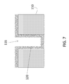
- FIGS. 7-9 are cross sectional views illustrating the formation of a contact according to another embodiment of the invention.
- FIG. 7 shows the W 120 conformally lining the via 115 .
- the W 120 may be deposited using atomic layer deposition (ALD), for example.
- ALD atomic layer deposition
- Depositing an interface metal 130 to completely fill the via 115 results in the structure shown in FIG. 8 .
- the interface metal 130 may be Co, Ni, Pd, Pt, or Ru for example.
- Polishing the W 120 and interface metal 130 results in the structure shown in FIG. 9 .
- the contact surface or interface 910 includes mostly interface metal 130 but also W 120 .
- FIGS. 10-13 are cross sectional views illustrating the formation of a contact according to yet another embodiment of the invention.
- FIG. 10 shows a W 120 fill in the via 115 formed within a dielectric layer 110 .
- a CMP process is performed on the W 120 fill to form a seam 1010 or narrow void in the W 120 fill.
- This seam 1010 is enlarged as shown in FIG. 11 .
- the enlargement may be achieved through oxidation of the W 120 at 500 to 600 degrees Celsius, for example, in an oxygen or nitrous oxide (N 2 O) plasma environment.
- Creating an opening 1210 in the enlarged seam 1010 results in the structure shown in FIG. 12 .
- the opening 1210 may be formed by dissolving tungsten (III) oxide (W 2 O 3 ) or tungsten trioxide (WO 3 ) in a high pH solution. In alternate embodiments to those shown in FIG. 12 , the shape and depth of the opening 1210 may be different than shown in FIG. 12 .
- a interface metal 130 fill in the opening 1210 followed by a CMP process results in the structure shown in FIG. 13 .
- the interface metal 130 may be Co, Ni, Pd, Pt, or Ru for example.
- the interface metal 130 fill may be preceded by a wet clean process to clean out W oxide from the opening 1210 .
- the contact surface or interface 1310 with the interconnect 135 indicates that the amount of interface metal 130 replacing W 120 is more similar to that of interface 610 than that of interface 910 .
- the interaction between W 120 and the interface metal 130 within the contact ( 120 / 130 ) is over a larger surface area in the embodiment shown in FIG. 13 .
- the resulting decrease in resistance due to the interface metal 130 replacing some of the W 120 at the interface 1310 with the interconnect 135 is likely to be more than that of the embodiment shown in FIG. 6 (interface 610 ) and less than that of the embodiment shown in FIG. 9 (interface 910 ).
- FIGS. 14-18 are cross sectional views illustrating the formation of a contact according to yet another embodiment of the invention.
- FIG. 14 shows a W 120 fill of a via 115 formed in a dielectric layer 110 , and a CMP process on the structure shown in FIG. 14 results in a standard contact as shown in FIG. 15 .
- an interconnect 135 would then be formed on this W 120 contact.
- W 120 at the interface with where the interconnect 135 would be formed (around the perimeter of the via 115 ) is oxidized to result in the structure shown in FIG. 16 .
- the W 120 is recessed to have an inverted-v shape such that more W 120 is recessed along the outer portions of the via 115 .
- the exposed W 120 has a larger surface area than the (flat) W 120 prior to oxidation.
- the oxidation may be performed under gas cluster ion beam (GCIB) exposure of the reactant gas (oxidizer), for example.
- GCIB gas cluster ion beam
- a wet clean process may then be performed to selectively remove oxidized W 120 .
- An interface metal 130 fill results in the structure shown in FIG. 17 .
- the portions of the via 115 in which oxidized W 120 is removed are now filled with interface metal 130 .
- a further CMP process results in the structure shown in FIG. 18 .
- the contact surface or interface 1810 with an interconnect 135 comprises only interface metal 130 and substantially no W 120 such that the interconnect 135 formed above the dielectric layer 110 would interface only with the interface metal 130 .
- more surface area interaction between W 120 and the interface metal 130 within the contact ( 120 / 130 ) is facilitated as compared to a uniform recess of the W 120 across the diameter of the via 115 .
- the combination of these two factors results in decreased resistance of the contact ( 120 / 130 ) shown in FIG. 18 (as compared with that in FIG. 15 ).
- FIG. 19 shows a cross sectional view of a portion of a semiconductor device according to an embodiment of the invention.
- FIG. 19 illustrates cross sectional views of three contacts ( 120 / 130 ).
- the contacts ( 120 / 130 ) are formed in vias ( 115 ) of a dielectric layer 110 formed over a semiconductor layer 105 .
- the W 120 portion of the contacts ( 120 / 130 ) is recessed in a v shape (rather than in an inverted-v shape, as in the embodiment of FIG. 18 ).
- the recessed portion is filled with interface metal 130 .
- the inverted-v shaped recess of the embodiment shown in FIG. 18 (and in contrast with the uniform recess of W 120 shown in FIG.
- the v-shaped recess of W 120 results in a larger surface area for interaction between the W 120 and the interface metal 130 filled in the recessed portion.
- the interconnects 135 formed above the contacts ( 120 / 130 ) interface only with the interface metal 130 (rather than with any W 120 ), like the embodiments shown in FIGS. 1 and 18 .
- a nitride cap 140 is formed conformally on the interconnects 135 , and a low-k dielectric 145 is formed on the dielectric layer 110 .
Abstract
Description
Claims (11)
Priority Applications (2)
| Application Number | Priority Date | Filing Date | Title |
|---|---|---|---|
| US14/749,811 US9786550B2 (en) | 2015-06-25 | 2015-06-25 | Low resistance metal contacts to interconnects |
| US14/949,386 US9799552B2 (en) | 2015-06-25 | 2015-11-23 | Low resistance metal contacts to interconnects |
Applications Claiming Priority (1)
| Application Number | Priority Date | Filing Date | Title |
|---|---|---|---|
| US14/749,811 US9786550B2 (en) | 2015-06-25 | 2015-06-25 | Low resistance metal contacts to interconnects |
Related Child Applications (1)
| Application Number | Title | Priority Date | Filing Date |
|---|---|---|---|
| US14/949,386 Continuation US9799552B2 (en) | 2015-06-25 | 2015-11-23 | Low resistance metal contacts to interconnects |
Publications (2)
| Publication Number | Publication Date |
|---|---|
| US20160379869A1 US20160379869A1 (en) | 2016-12-29 |
| US9786550B2 true US9786550B2 (en) | 2017-10-10 |
Family
ID=57602821
Family Applications (2)
| Application Number | Title | Priority Date | Filing Date |
|---|---|---|---|
| US14/749,811 Active US9786550B2 (en) | 2015-06-25 | 2015-06-25 | Low resistance metal contacts to interconnects |
| US14/949,386 Active 2035-07-01 US9799552B2 (en) | 2015-06-25 | 2015-11-23 | Low resistance metal contacts to interconnects |
Family Applications After (1)
| Application Number | Title | Priority Date | Filing Date |
|---|---|---|---|
| US14/949,386 Active 2035-07-01 US9799552B2 (en) | 2015-06-25 | 2015-11-23 | Low resistance metal contacts to interconnects |
Country Status (1)
| Country | Link |
|---|---|
| US (2) | US9786550B2 (en) |
Cited By (4)
| Publication number | Priority date | Publication date | Assignee | Title |
|---|---|---|---|---|
| US10373866B1 (en) | 2018-05-04 | 2019-08-06 | International Business Machines Corporation | Method of forming metal insulator metal capacitor with extended capacitor plates |
| US10381263B1 (en) | 2018-05-04 | 2019-08-13 | International Business Machines Corporation | Method of forming via contact with resistance control |
| US10529663B1 (en) | 2018-10-14 | 2020-01-07 | International Business Machines Corporation | Copper interconnect with filled void |
| US10937732B2 (en) | 2018-09-11 | 2021-03-02 | Samsung Electronics Co., Ltd. | Semiconductor devices including contacts and conductive line interfaces with contacting sidewalls |
Families Citing this family (3)
| Publication number | Priority date | Publication date | Assignee | Title |
|---|---|---|---|---|
| US20170186747A1 (en) * | 2015-12-29 | 2017-06-29 | International Business Machines Corporation | STRUCTURE AND METHOD FOR SiGe FIN FORMATION IN A SEMICONDUCTOR DEVICE |
| CN108447836A (en) * | 2017-02-15 | 2018-08-24 | 联华电子股份有限公司 | Contact pad structure and preparation method thereof |
| KR20220117469A (en) | 2021-02-17 | 2022-08-24 | 삼성전자주식회사 | Semiconductor device and method for fabricating the same |
Citations (18)
| Publication number | Priority date | Publication date | Assignee | Title |
|---|---|---|---|---|
| US20020121699A1 (en) | 2001-03-01 | 2002-09-05 | Kuan-Lun Cheng | Dual damascene Cu contact plug using selective tungsten deposition |
| US20060170020A1 (en) * | 2005-01-28 | 2006-08-03 | Katsuyuki Ohta | Semiconductor memory device and method for fabricating the same |
| US7180193B2 (en) | 2004-04-13 | 2007-02-20 | Taiwan Semiconductor Manufacturing Company, Ltd. | Via recess in underlying conductive line |
| US20080076230A1 (en) * | 2006-09-21 | 2008-03-27 | Kangguo Cheng | Trench Capacitor with Void-Free Conductor Fill |
| US20080311718A1 (en) * | 2007-06-15 | 2008-12-18 | Renesas Technology Corp. | Manufacturing method of semiconductor device |
| US20090075472A1 (en) * | 2007-09-19 | 2009-03-19 | International Business Machines Corporation | Methods to mitigate plasma damage in organosilicate dielectrics |
| US7528066B2 (en) | 2006-03-01 | 2009-05-05 | International Business Machines Corporation | Structure and method for metal integration |
| US20090302473A1 (en) * | 2008-02-07 | 2009-12-10 | Panasonic Corporation | Semiconductor device and manufacturing method thereof |
| US20100081272A1 (en) * | 2008-09-30 | 2010-04-01 | Samsung Electronics Co., Ltd. | Methods of Forming Electrical Interconnects Using Electroless Plating Techniques that Inhibit Void Formation |
| US7732922B2 (en) | 2008-01-07 | 2010-06-08 | International Business Machines Corporation | Simultaneous grain modulation for BEOL applications |
| US7843063B2 (en) | 2008-02-14 | 2010-11-30 | International Business Machines Corporation | Microstructure modification in copper interconnect structure |
| US8021974B2 (en) | 2009-01-09 | 2011-09-20 | Internatioanl Business Machines Corporation | Structure and method for back end of the line integration |
| US8232647B2 (en) | 2008-02-21 | 2012-07-31 | International Business Machines Corporation | Structure and process for metallization in high aspect ratio features |
| US20130320544A1 (en) * | 2012-05-29 | 2013-12-05 | International Business Machines Corporation | Corrosion/etching protection in integration circuit fabrications |
| US20140183738A1 (en) | 2012-12-28 | 2014-07-03 | Christopher J. Jezewski | Cobalt based interconnects and methods of fabrication thereof |
| US20140327140A1 (en) * | 2013-05-03 | 2014-11-06 | GlobalFoundries, Inc. | Integrated circuits and methods for fabricating integrated circuits with improved contact structures |
| US9142505B2 (en) * | 2013-06-18 | 2015-09-22 | Taiwan Semiconductor Manufacturing Company, Ltd. | Method and apparatus for back end of line semiconductor device processing |
| US20150318243A1 (en) * | 2014-04-30 | 2015-11-05 | Taiwan Semiconductor Manufacturing Company, Ltd. | Composite Contact Plug Structure and Method of Making Same |
Family Cites Families (3)
| Publication number | Priority date | Publication date | Assignee | Title |
|---|---|---|---|---|
| TW347570B (en) * | 1996-12-24 | 1998-12-11 | Toshiba Co Ltd | Semiconductor device and method for manufacturing the same |
| US20060252252A1 (en) * | 2005-03-18 | 2006-11-09 | Zhize Zhu | Electroless deposition processes and compositions for forming interconnects |
| WO2007020686A1 (en) * | 2005-08-15 | 2007-02-22 | Fujitsu Limited | Semiconductor device and method for manufacturing same |
-
2015
- 2015-06-25 US US14/749,811 patent/US9786550B2/en active Active
- 2015-11-23 US US14/949,386 patent/US9799552B2/en active Active
Patent Citations (18)
| Publication number | Priority date | Publication date | Assignee | Title |
|---|---|---|---|---|
| US20020121699A1 (en) | 2001-03-01 | 2002-09-05 | Kuan-Lun Cheng | Dual damascene Cu contact plug using selective tungsten deposition |
| US7180193B2 (en) | 2004-04-13 | 2007-02-20 | Taiwan Semiconductor Manufacturing Company, Ltd. | Via recess in underlying conductive line |
| US20060170020A1 (en) * | 2005-01-28 | 2006-08-03 | Katsuyuki Ohta | Semiconductor memory device and method for fabricating the same |
| US7528066B2 (en) | 2006-03-01 | 2009-05-05 | International Business Machines Corporation | Structure and method for metal integration |
| US20080076230A1 (en) * | 2006-09-21 | 2008-03-27 | Kangguo Cheng | Trench Capacitor with Void-Free Conductor Fill |
| US20080311718A1 (en) * | 2007-06-15 | 2008-12-18 | Renesas Technology Corp. | Manufacturing method of semiconductor device |
| US20090075472A1 (en) * | 2007-09-19 | 2009-03-19 | International Business Machines Corporation | Methods to mitigate plasma damage in organosilicate dielectrics |
| US7732922B2 (en) | 2008-01-07 | 2010-06-08 | International Business Machines Corporation | Simultaneous grain modulation for BEOL applications |
| US20090302473A1 (en) * | 2008-02-07 | 2009-12-10 | Panasonic Corporation | Semiconductor device and manufacturing method thereof |
| US7843063B2 (en) | 2008-02-14 | 2010-11-30 | International Business Machines Corporation | Microstructure modification in copper interconnect structure |
| US8232647B2 (en) | 2008-02-21 | 2012-07-31 | International Business Machines Corporation | Structure and process for metallization in high aspect ratio features |
| US20100081272A1 (en) * | 2008-09-30 | 2010-04-01 | Samsung Electronics Co., Ltd. | Methods of Forming Electrical Interconnects Using Electroless Plating Techniques that Inhibit Void Formation |
| US8021974B2 (en) | 2009-01-09 | 2011-09-20 | Internatioanl Business Machines Corporation | Structure and method for back end of the line integration |
| US20130320544A1 (en) * | 2012-05-29 | 2013-12-05 | International Business Machines Corporation | Corrosion/etching protection in integration circuit fabrications |
| US20140183738A1 (en) | 2012-12-28 | 2014-07-03 | Christopher J. Jezewski | Cobalt based interconnects and methods of fabrication thereof |
| US20140327140A1 (en) * | 2013-05-03 | 2014-11-06 | GlobalFoundries, Inc. | Integrated circuits and methods for fabricating integrated circuits with improved contact structures |
| US9142505B2 (en) * | 2013-06-18 | 2015-09-22 | Taiwan Semiconductor Manufacturing Company, Ltd. | Method and apparatus for back end of line semiconductor device processing |
| US20150318243A1 (en) * | 2014-04-30 | 2015-11-05 | Taiwan Semiconductor Manufacturing Company, Ltd. | Composite Contact Plug Structure and Method of Making Same |
Non-Patent Citations (4)
| Title |
|---|
| Anik et al., "Effect of pH on the Anodic Behavior of Tungsten", Journal of the Electrochemical Society, vol. 149, No. 6, 2002, pp. B224-B233. |
| List of IBM Patents or Patent Applications Treated as Related; (Appendix P), Filed Jan. 7, 2016; 2 pages. |
| Stephen M. Gates et al., "Low Resistance Metal Contacts to Interconnects", U.S. Appl. No. 14/949,386, filed Nov. 23, 2015. |
| Yang et al., "Effects of Contact Area on Mechanical Strength, Electrical Resistance, and Electromigration Reliability of Cu/Low-k Interconnects", Electrochemical and Solid-State Letters, vol. 13, No. 6, 2010, pp. H197-H199. |
Cited By (8)
| Publication number | Priority date | Publication date | Assignee | Title |
|---|---|---|---|---|
| US10373866B1 (en) | 2018-05-04 | 2019-08-06 | International Business Machines Corporation | Method of forming metal insulator metal capacitor with extended capacitor plates |
| US10381263B1 (en) | 2018-05-04 | 2019-08-13 | International Business Machines Corporation | Method of forming via contact with resistance control |
| US10559649B2 (en) | 2018-05-04 | 2020-02-11 | International Business Machines Corporation | Metal insulator metal capacitor with extended capacitor plates |
| US10685915B2 (en) | 2018-05-04 | 2020-06-16 | International Business Machines Corporation | Via contact resistance control |
| US10998227B2 (en) | 2018-05-04 | 2021-05-04 | International Business Machines Corporation | Metal insulator metal capacitor with extended capacitor plates |
| US10937732B2 (en) | 2018-09-11 | 2021-03-02 | Samsung Electronics Co., Ltd. | Semiconductor devices including contacts and conductive line interfaces with contacting sidewalls |
| US11502033B2 (en) | 2018-09-11 | 2022-11-15 | Samsung Electronics Co., Ltd. | Semiconductor devices including contacts and conductive line interfaces with contacting sidewalls |
| US10529663B1 (en) | 2018-10-14 | 2020-01-07 | International Business Machines Corporation | Copper interconnect with filled void |
Also Published As
| Publication number | Publication date |
|---|---|
| US20160379869A1 (en) | 2016-12-29 |
| US20160379880A1 (en) | 2016-12-29 |
| US9799552B2 (en) | 2017-10-24 |
Similar Documents
| Publication | Publication Date | Title |
|---|---|---|
| US9786550B2 (en) | Low resistance metal contacts to interconnects | |
| CN103515304B (en) | Without the dual damascene metal interconnection part of etch damage and Department of Electronics's irrespective of size (ESL) | |
| TWI588986B (en) | Nram arrays with nanotube blocks, nanotube traces, and nanotube planes and methods of making same | |
| US9768113B2 (en) | Self aligned via in integrated circuit | |
| US7842600B2 (en) | Methods of forming interlayer dielectrics having air gaps | |
| US9431345B2 (en) | Semiconductor device and method of manufacturing the same | |
| JP2010503191A (en) | Controlling carbon nanostructure growth in interconnected structures | |
| US10651078B2 (en) | Selective ILD deposition for fully aligned via with airgap | |
| US8921975B2 (en) | System and method for forming aluminum fuse for compatibility with copper BEOL interconnect scheme | |
| US20060208362A1 (en) | Carbon nanotubes with controlled diameter, length, and metallic contacts | |
| TWI505359B (en) | Semiconductor devices and methods of forming same | |
| US7105851B2 (en) | Nanotubes for integrated circuits | |
| JP2016058521A (en) | Semiconductor device and manufacturing method of the same | |
| US7638423B2 (en) | Semiconductor device and method of forming wires of semiconductor device | |
| US20140147942A1 (en) | Memory device and method for manufacturing the same | |
| CN105531812B (en) | The super thin metal line formed by selective deposition | |
| US9536832B1 (en) | Junctionless back end of the line via contact | |
| US9659869B2 (en) | Forming barrier walls, capping, or alloys /compounds within metal lines | |
| US9484206B2 (en) | Semiconductor device including catalyst layer and graphene layer thereon and method for manufacturing the same | |
| TWI811782B (en) | Semiconductor structure and forming method thereof | |
| JP2008172250A (en) | Electrical wire structure having carbon nanotube and method for forming structure | |
| JP2022027620A (en) | Semiconductor device structure and formation method for the same | |
| KR100713916B1 (en) | Method of manufacturing semiconductor device | |
| US11410926B2 (en) | E-fuse enhancement by underlayer layout design | |
| US20220375859A1 (en) | E-Fuse Enhancement By Underlayer Layout Design |
Legal Events
| Date | Code | Title | Description |
|---|---|---|---|
| AS | Assignment |
Owner name: INTERNATIONAL BUSINESS MACHINES CORPORATION, NEW Y Free format text: ASSIGNMENT OF ASSIGNORS INTEREST;ASSIGNORS:GATES, STEPHEN M.;FRITZ, GREGORY M.;JOSEPH, ERIC A.;AND OTHERS;SIGNING DATES FROM 20150616 TO 20150623;REEL/FRAME:035965/0683 |
|
| STCF | Information on status: patent grant |
Free format text: PATENTED CASE |
|
| AS | Assignment |
Owner name: TESSERA, INC., CALIFORNIA Free format text: ASSIGNMENT OF ASSIGNORS INTEREST;ASSIGNOR:INTERNATIONAL BUSINESS MACHINES CORPORATION;REEL/FRAME:051489/0557 Effective date: 20191227 |
|
| AS | Assignment |
Owner name: BANK OF AMERICA, N.A., NORTH CAROLINA Free format text: SECURITY INTEREST;ASSIGNORS:ROVI SOLUTIONS CORPORATION;ROVI TECHNOLOGIES CORPORATION;ROVI GUIDES, INC.;AND OTHERS;REEL/FRAME:053468/0001 Effective date: 20200601 |
|
| MAFP | Maintenance fee payment |
Free format text: PAYMENT OF MAINTENANCE FEE, 4TH YEAR, LARGE ENTITY (ORIGINAL EVENT CODE: M1551); ENTITY STATUS OF PATENT OWNER: LARGE ENTITY Year of fee payment: 4 |