US9763370B2 - Apparatus for assembly of microelectronic devices - Google Patents
Apparatus for assembly of microelectronic devices Download PDFInfo
- Publication number
- US9763370B2 US9763370B2 US14/088,725 US201314088725A US9763370B2 US 9763370 B2 US9763370 B2 US 9763370B2 US 201314088725 A US201314088725 A US 201314088725A US 9763370 B2 US9763370 B2 US 9763370B2
- Authority
- US
- United States
- Prior art keywords
- microelectronic devices
- substrate
- roller
- microelectronic
- layer
- Prior art date
- Legal status (The legal status is an assumption and is not a legal conclusion. Google has not performed a legal analysis and makes no representation as to the accuracy of the status listed.)
- Active, expires
Links
Images


Classifications
-
- H—ELECTRICITY
- H05—ELECTRIC TECHNIQUES NOT OTHERWISE PROVIDED FOR
- H05K—PRINTED CIRCUITS; CASINGS OR CONSTRUCTIONAL DETAILS OF ELECTRIC APPARATUS; MANUFACTURE OF ASSEMBLAGES OF ELECTRICAL COMPONENTS
- H05K13/00—Apparatus or processes specially adapted for manufacturing or adjusting assemblages of electric components
- H05K13/04—Mounting of components, e.g. of leadless components
- H05K13/0478—Simultaneously mounting of different components
-
- B—PERFORMING OPERATIONS; TRANSPORTING
- B65—CONVEYING; PACKING; STORING; HANDLING THIN OR FILAMENTARY MATERIAL
- B65G—TRANSPORT OR STORAGE DEVICES, e.g. CONVEYORS FOR LOADING OR TIPPING, SHOP CONVEYOR SYSTEMS OR PNEUMATIC TUBE CONVEYORS
- B65G47/00—Article or material-handling devices associated with conveyors; Methods employing such devices
- B65G47/74—Feeding, transfer, or discharging devices of particular kinds or types
- B65G47/84—Star-shaped wheels or devices having endless travelling belts or chains, the wheels or devices being equipped with article-engaging elements
- B65G47/846—Star-shaped wheels or wheels equipped with article-engaging elements
- B65G47/847—Star-shaped wheels or wheels equipped with article-engaging elements the article-engaging elements being grippers
-
- B—PERFORMING OPERATIONS; TRANSPORTING
- B65—CONVEYING; PACKING; STORING; HANDLING THIN OR FILAMENTARY MATERIAL
- B65G—TRANSPORT OR STORAGE DEVICES, e.g. CONVEYORS FOR LOADING OR TIPPING, SHOP CONVEYOR SYSTEMS OR PNEUMATIC TUBE CONVEYORS
- B65G47/00—Article or material-handling devices associated with conveyors; Methods employing such devices
- B65G47/74—Feeding, transfer, or discharging devices of particular kinds or types
- B65G47/84—Star-shaped wheels or devices having endless travelling belts or chains, the wheels or devices being equipped with article-engaging elements
- B65G47/846—Star-shaped wheels or wheels equipped with article-engaging elements
- B65G47/848—Star-shaped wheels or wheels equipped with article-engaging elements the article-engaging elements being suction or magnetic means
-
- H01L21/2007—
-
- H01L21/67132—
-
- H01L21/67242—
-
- H01L21/673—
-
- H01L21/67796—
-
- H01L24/75—
-
- H01L24/81—
-
- H01L31/022441—
-
- H01L31/0516—
-
- H01L31/0682—
-
- H01L31/188—
-
- H—ELECTRICITY
- H05—ELECTRIC TECHNIQUES NOT OTHERWISE PROVIDED FOR
- H05K—PRINTED CIRCUITS; CASINGS OR CONSTRUCTIONAL DETAILS OF ELECTRIC APPARATUS; MANUFACTURE OF ASSEMBLAGES OF ELECTRICAL COMPONENTS
- H05K3/00—Apparatus or processes for manufacturing printed circuits
- H05K3/30—Assembling printed circuits with electric components, e.g. with resistors
- H05K3/301—Assembling printed circuits with electric components, e.g. with resistors by means of a mounting structure
-
- H—ELECTRICITY
- H05—ELECTRIC TECHNIQUES NOT OTHERWISE PROVIDED FOR
- H05K—PRINTED CIRCUITS; CASINGS OR CONSTRUCTIONAL DETAILS OF ELECTRIC APPARATUS; MANUFACTURE OF ASSEMBLAGES OF ELECTRICAL COMPONENTS
- H05K3/00—Apparatus or processes for manufacturing printed circuits
- H05K3/30—Assembling printed circuits with electric components, e.g. with resistors
- H05K3/303—Assembling printed circuits with electric components, e.g. with resistors with surface mounted components
-
- H—ELECTRICITY
- H10—SEMICONDUCTOR DEVICES; ELECTRIC SOLID-STATE DEVICES NOT OTHERWISE PROVIDED FOR
- H10F—INORGANIC SEMICONDUCTOR DEVICES SENSITIVE TO INFRARED RADIATION, LIGHT, ELECTROMAGNETIC RADIATION OF SHORTER WAVELENGTH OR CORPUSCULAR RADIATION
- H10F10/00—Individual photovoltaic cells, e.g. solar cells
- H10F10/10—Individual photovoltaic cells, e.g. solar cells having potential barriers
- H10F10/14—Photovoltaic cells having only PN homojunction potential barriers
- H10F10/146—Back-junction photovoltaic cells, e.g. having interdigitated base-emitter regions on the back side
-
- H—ELECTRICITY
- H10—SEMICONDUCTOR DEVICES; ELECTRIC SOLID-STATE DEVICES NOT OTHERWISE PROVIDED FOR
- H10F—INORGANIC SEMICONDUCTOR DEVICES SENSITIVE TO INFRARED RADIATION, LIGHT, ELECTROMAGNETIC RADIATION OF SHORTER WAVELENGTH OR CORPUSCULAR RADIATION
- H10F19/00—Integrated devices, or assemblies of multiple devices, comprising at least one photovoltaic cell covered by group H10F10/00, e.g. photovoltaic modules
- H10F19/90—Structures for connecting between photovoltaic cells, e.g. interconnections or insulating spacers
- H10F19/902—Structures for connecting between photovoltaic cells, e.g. interconnections or insulating spacers for series or parallel connection of photovoltaic cells
- H10F19/908—Structures for connecting between photovoltaic cells, e.g. interconnections or insulating spacers for series or parallel connection of photovoltaic cells for back-contact photovoltaic cells
-
- H—ELECTRICITY
- H10—SEMICONDUCTOR DEVICES; ELECTRIC SOLID-STATE DEVICES NOT OTHERWISE PROVIDED FOR
- H10F—INORGANIC SEMICONDUCTOR DEVICES SENSITIVE TO INFRARED RADIATION, LIGHT, ELECTROMAGNETIC RADIATION OF SHORTER WAVELENGTH OR CORPUSCULAR RADIATION
- H10F71/00—Manufacture or treatment of devices covered by this subclass
- H10F71/137—Batch treatment of the devices
- H10F71/1375—Apparatus for automatic interconnection of photovoltaic cells in a module
-
- H—ELECTRICITY
- H10—SEMICONDUCTOR DEVICES; ELECTRIC SOLID-STATE DEVICES NOT OTHERWISE PROVIDED FOR
- H10F—INORGANIC SEMICONDUCTOR DEVICES SENSITIVE TO INFRARED RADIATION, LIGHT, ELECTROMAGNETIC RADIATION OF SHORTER WAVELENGTH OR CORPUSCULAR RADIATION
- H10F77/00—Constructional details of devices covered by this subclass
- H10F77/20—Electrodes
- H10F77/206—Electrodes for devices having potential barriers
- H10F77/211—Electrodes for devices having potential barriers for photovoltaic cells
- H10F77/219—Arrangements for electrodes of back-contact photovoltaic cells
-
- H—ELECTRICITY
- H10—SEMICONDUCTOR DEVICES; ELECTRIC SOLID-STATE DEVICES NOT OTHERWISE PROVIDED FOR
- H10P—GENERIC PROCESSES OR APPARATUS FOR THE MANUFACTURE OR TREATMENT OF DEVICES COVERED BY CLASS H10
- H10P72/00—Handling or holding of wafers, substrates or devices during manufacture or treatment thereof
- H10P72/04—Apparatus for manufacture or treatment
- H10P72/0442—Apparatus for placing on an insulating substrate, e.g. tape
-
- H—ELECTRICITY
- H10—SEMICONDUCTOR DEVICES; ELECTRIC SOLID-STATE DEVICES NOT OTHERWISE PROVIDED FOR
- H10P—GENERIC PROCESSES OR APPARATUS FOR THE MANUFACTURE OR TREATMENT OF DEVICES COVERED BY CLASS H10
- H10P72/00—Handling or holding of wafers, substrates or devices during manufacture or treatment thereof
- H10P72/06—Apparatus for monitoring, sorting, marking, testing or measuring
-
- H—ELECTRICITY
- H10—SEMICONDUCTOR DEVICES; ELECTRIC SOLID-STATE DEVICES NOT OTHERWISE PROVIDED FOR
- H10P—GENERIC PROCESSES OR APPARATUS FOR THE MANUFACTURE OR TREATMENT OF DEVICES COVERED BY CLASS H10
- H10P72/00—Handling or holding of wafers, substrates or devices during manufacture or treatment thereof
- H10P72/10—Handling or holding of wafers, substrates or devices during manufacture or treatment thereof using carriers specially adapted therefor, e.g. front opening unified pods [FOUP]
-
- H—ELECTRICITY
- H10—SEMICONDUCTOR DEVICES; ELECTRIC SOLID-STATE DEVICES NOT OTHERWISE PROVIDED FOR
- H10P—GENERIC PROCESSES OR APPARATUS FOR THE MANUFACTURE OR TREATMENT OF DEVICES COVERED BY CLASS H10
- H10P72/00—Handling or holding of wafers, substrates or devices during manufacture or treatment thereof
- H10P72/30—Handling or holding of wafers, substrates or devices during manufacture or treatment thereof for conveying, e.g. between different workstations
- H10P72/38—Handling or holding of wafers, substrates or devices during manufacture or treatment thereof for conveying, e.g. between different workstations with angular orientation of workpieces
-
- H—ELECTRICITY
- H10—SEMICONDUCTOR DEVICES; ELECTRIC SOLID-STATE DEVICES NOT OTHERWISE PROVIDED FOR
- H10P—GENERIC PROCESSES OR APPARATUS FOR THE MANUFACTURE OR TREATMENT OF DEVICES COVERED BY CLASS H10
- H10P90/00—Preparation of wafers not covered by a single main group of this subclass, e.g. wafer reinforcement
- H10P90/19—Preparing inhomogeneous wafers
- H10P90/1904—Preparing vertically inhomogeneous wafers
- H10P90/1906—Preparing SOI wafers
- H10P90/1914—Preparing SOI wafers using bonding
-
- H—ELECTRICITY
- H10—SEMICONDUCTOR DEVICES; ELECTRIC SOLID-STATE DEVICES NOT OTHERWISE PROVIDED FOR
- H10W—GENERIC PACKAGES, INTERCONNECTIONS, CONNECTORS OR OTHER CONSTRUCTIONAL DETAILS OF DEVICES COVERED BY CLASS H10
- H10W72/00—Interconnections or connectors in packages
- H10W72/071—Connecting or disconnecting
- H10W72/072—Connecting or disconnecting of bump connectors
-
- H01L2924/00—
-
- H01L2924/12032—
-
- H01L2924/12042—
-
- H01L2924/1301—
-
- H01L2924/13033—
-
- H01L2924/13034—
-
- H01L2924/1305—
-
- H01L2924/13055—
-
- H—ELECTRICITY
- H10—SEMICONDUCTOR DEVICES; ELECTRIC SOLID-STATE DEVICES NOT OTHERWISE PROVIDED FOR
- H10W—GENERIC PACKAGES, INTERCONNECTIONS, CONNECTORS OR OTHER CONSTRUCTIONAL DETAILS OF DEVICES COVERED BY CLASS H10
- H10W72/00—Interconnections or connectors in packages
- H10W72/071—Connecting or disconnecting
- H10W72/0711—Apparatus therefor
-
- Y—GENERAL TAGGING OF NEW TECHNOLOGICAL DEVELOPMENTS; GENERAL TAGGING OF CROSS-SECTIONAL TECHNOLOGIES SPANNING OVER SEVERAL SECTIONS OF THE IPC; TECHNICAL SUBJECTS COVERED BY FORMER USPC CROSS-REFERENCE ART COLLECTIONS [XRACs] AND DIGESTS
- Y02—TECHNOLOGIES OR APPLICATIONS FOR MITIGATION OR ADAPTATION AGAINST CLIMATE CHANGE
- Y02E—REDUCTION OF GREENHOUSE GAS [GHG] EMISSIONS, RELATED TO ENERGY GENERATION, TRANSMISSION OR DISTRIBUTION
- Y02E10/00—Energy generation through renewable energy sources
- Y02E10/50—Photovoltaic [PV] energy
- Y02E10/547—Monocrystalline silicon PV cells
-
- Y—GENERAL TAGGING OF NEW TECHNOLOGICAL DEVELOPMENTS; GENERAL TAGGING OF CROSS-SECTIONAL TECHNOLOGIES SPANNING OVER SEVERAL SECTIONS OF THE IPC; TECHNICAL SUBJECTS COVERED BY FORMER USPC CROSS-REFERENCE ART COLLECTIONS [XRACs] AND DIGESTS
- Y10—TECHNICAL SUBJECTS COVERED BY FORMER USPC
- Y10T—TECHNICAL SUBJECTS COVERED BY FORMER US CLASSIFICATION
- Y10T29/00—Metal working
- Y10T29/49—Method of mechanical manufacture
- Y10T29/49002—Electrical device making
-
- Y—GENERAL TAGGING OF NEW TECHNOLOGICAL DEVELOPMENTS; GENERAL TAGGING OF CROSS-SECTIONAL TECHNOLOGIES SPANNING OVER SEVERAL SECTIONS OF THE IPC; TECHNICAL SUBJECTS COVERED BY FORMER USPC CROSS-REFERENCE ART COLLECTIONS [XRACs] AND DIGESTS
- Y10—TECHNICAL SUBJECTS COVERED BY FORMER USPC
- Y10T—TECHNICAL SUBJECTS COVERED BY FORMER US CLASSIFICATION
- Y10T29/00—Metal working
- Y10T29/53—Means to assemble or disassemble
- Y10T29/5313—Means to assemble electrical device
- Y10T29/53174—Means to fasten electrical component to wiring board, base, or substrate
- Y10T29/53178—Chip component
-
- Y—GENERAL TAGGING OF NEW TECHNOLOGICAL DEVELOPMENTS; GENERAL TAGGING OF CROSS-SECTIONAL TECHNOLOGIES SPANNING OVER SEVERAL SECTIONS OF THE IPC; TECHNICAL SUBJECTS COVERED BY FORMER USPC CROSS-REFERENCE ART COLLECTIONS [XRACs] AND DIGESTS
- Y10—TECHNICAL SUBJECTS COVERED BY FORMER USPC
- Y10T—TECHNICAL SUBJECTS COVERED BY FORMER US CLASSIFICATION
- Y10T29/00—Metal working
- Y10T29/53—Means to assemble or disassemble
- Y10T29/5313—Means to assemble electrical device
- Y10T29/53191—Means to apply vacuum directly to position or hold work part
Definitions
- the present invention relates in general to a process and system for placement of microelectronic devices on a variety of substrates, more specifically, for massively parallel placement of solar cells onto a module. Other embodiments are also described and claimed.
- the assembly of solar cells into a module is one of the key steps.
- Relatively small (500 micrometers or less) thin solar cells can be assembled into large arrays using mechanical and surface chemistry driven techniques.
- the details and associated cost of this assembly step is critical in determining the limitations of desirable solar cell size.
- pick-and-place assembly techniques in which a machine is used to individually pick up, arrange and place each device on a substrate, the assembly costs are per device.
- larger cell sizes 500 micrometers-1 mm
- the devices are PV cells that are transferred onto a roller with pre-determined locations and deposited onto a receiving substrate using a “printing-like” technique.
- the cells can be placed onto the roller with the cell contacts facing into openings formed on the roller or with the contacts facing out.
- a roller having a different pattern of openings and a different receiving substrate may be used.
- the conducting and insulating layers can also be patterned with openings to generate series and/or parallel combinations of cells to achieve a robust, high performance panel assembly of cells.
- the conducting/insulating layers can be pre-patterned to match the electrical contacts on the cells.
- the insulating layers can be then slightly re-flown to infiltrate and fill up any voids that might remain in the assembly, which will improve the mechanical stability and reliability of the assembly.
- the electrical contacts formed on the cells e.g. top surface of the wafer
- the electrical contacts formed on the cells which need to be electrically separate are formed on different height surfaces, which will allow them to be contacted separated by other devices and/or circuitry.
- the method includes positioning a microelectronic device on a carrier substrate and coupling the microelectronic device to a roller assembly. Once coupled, the roller assembly is rotated to transport the microelectronic device from the carrier substrate to a receiving substrate.
- the system includes a carrier substrate configured to support a microelectronic device and a roller assembly configured to receive and transport the microelectronic device.
- the system further includes a receiving substrate dimensioned to receive the microelectronic device from the roller assembly.
- the apparatus for parallel assembly of microelectronic devices on a module may include a laterally translatable carrier substrate configured to move a plurality of microelectronic devices in a first direction.
- the apparatus may further include a rotatable cylindrical body having a plurality of device openings dimensioned to receive the microelectronic devices and a laterally translatable receiving substrate configured to move in a second direction.
- FIG. 1 schematically illustrates a cross-sectional side view of one embodiment of a microelectronic device transport system.
- FIG. 2 schematically illustrates a front perspective view of the system of FIG. 1 .
- FIG. 3 schematically illustrates a cross-sectional side view of a microelectronic device on a substrate.
- FIG. 4 schematically illustrates a cross-sectional side view of the microelectronic device of FIG. 3 after application of an insulating layer.
- FIG. 5 schematically illustrates a cross-sectional side view of the microelectronic device of FIG. 4 after application of a conductive layer.
- FIG. 6 schematically illustrates a cross-sectional side view of the microelectronic device of FIG. 5 after application of an insulating layer.
- FIG. 7 schematically illustrates a cross-sectional side view of the microelectronic device of FIG. 6 after application of a conductive layer.
- FIG. 8 schematically illustrates a cross-sectional side view of the microelectronic device of FIG. 7 after application of an insulating layer.
- FIG. 9 schematically illustrates a cross-sectional side view of another embodiment of a microelectronic device transport system.
- FIG. 10 schematically illustrates a cross-sectional side view of one embodiment of a microelectronic device.
- FIG. 1 schematically illustrates a cross-sectional side view of one embodiment of a microelectronic device transport system.
- system 100 is a system capable of massively parallel placement of microelectronic devices on a variety of surfaces (e.g., substrates, panels, modules or the like).
- system 100 is capable of picking up and transporting a plurality of microelectronic devices simultaneously from one substrate and placing them on another substrate for further processing.
- system 100 transports the plurality of microelectronic devices using a “printing-like” technique.
- system 100 may be configured to “print” the microelectronic devices onto a desired substrate.
- system 100 may include a roller assembly 102 , which is positioned between a carrier substrate 104 and a receiving substrate 106 .
- Roller assembly 102 may include roller 108 which is similar to a gravure cylinder used in gravure printing.
- roller 108 may be a metal (e.g. steel) or rubber cylinder which can be engraved or otherwise machined to include a desired pattern along its outer surface. The pattern allows for roller 108 to pick up microelectronic devices and “print” (i.e. place) the devices onto another surface.
- roller 108 may be assembled within system 100 such that it can rotate around a central axis 110 .
- central axis 110 may be a fixed axis such that roller 108 remains in the same lateral position while rotating.
- roller 108 may rotate about axis 110 in a clockwise direction as illustrated by arrow 112 .
- Roller 108 may, however, be movable in a vertical direction to allow for vertical positioning of roller 108 within system 100 .
- roller 108 may be fixed in both a lateral and a vertical direction, or movable in one or both directions.
- Rotation of roller 108 may be driven by an actuating mechanism 140 , such as, for example, a motor assembly or any similar actuating mechanism capable of driving rotation of an associated roller.
- Roller 108 may be positioned between carrier substrate 104 and receiving substrate 106 and include device openings 114 A, 114 B, 114 C, 114 D, 114 E, 114 F and 114 G along its outer surface.
- Device openings 114 A, 114 B, 114 C, 114 D, 114 E, 114 F and 114 G may be dimensioned to receive microelectronic devices 116 A, 116 B, 116 C, 116 D, 116 E, 116 F and 116 G, respectively.
- microelectronic devices 116 A- 116 G are photovoltaic solar cells
- device openings 114 A- 114 G may be recessed regions within the surface of roller 108 which have a similar shape to photovoltaic solar cells such that the cells can be received therein.
- microelectronic device 116 G is a multilayer photovoltaic solar cell including a substrate layer 118 , an insulator 120 formed on the substrate layer 118 and contact pads 122 A, 1228 and 122 C formed on the substrate layer 118 and insulator 120 .
- the remaining microelectronic devices 116 A- 116 F may have similar features.
- Device openings 114 A- 114 G may therefore have a size and shape matching the profile of each of the multilayered microelectronic devices 116 A- 116 G.
- Device openings 114 A- 114 G may, however, have a size and shape similar to, and capable of receiving, other types of microelectronic devices, for example, a detector device, an integrated circuit device or the like.
- Device openings 114 A- 114 G may be formed within a surface of roller 108 according to any conventional processing technique capable of forming micro-scale recesses (e.g. 1 mm or less) within a surface of roller 108 , for example, machining, laser imprinting, engraving, patterning, etching, or the like. It is further to be understood that although 7 device openings 114 A- 114 G are illustrated, any number of device openings, and in any desired spacing, may be formed around the outer surface of roller 108 .
- roller 108 is an elongated cylinder and includes multiple device openings along its length, as shown in FIG. 2 .
- FIG. 2 illustrates a front perspective view of system 100 , with carrier substrate 104 and microelectronic devices 116 A- 116 G removed for ease of illustration. From this view, it can be seen that roller 108 includes an array of device openings, including openings 114 A- 114 G (some not shown), positioned around the circumference of roller 108 and extending along its length from one end to the other. Thus, it is to be understood that any number and arrangement of device openings may be formed in roller 108 .
- the number and/or arrangement of device openings may be determined based on the desired number and/or arrangement of microelectronic devices on the receiving substrate. For example, where the microelectronic devices are desired to be distributed onto the receiving substrate in a specific pattern, roller 108 may have device openings which match the desired pattern and therefore pick up the microelectronic devices and distribute them in the desired pattern on the receiving substrate. As such, the number and/or arrangement of device openings is only constrained by the number of microelectronic devices desired to be picked up and transported by roller 108 .
- microelectronic devices 116 A- 116 G may be dispersed along the entire length and width of carrier substrate 104 such that they are spread out along the length of roller 108 and can be received by any of the device openings they may come in contact with.
- roller 108 is positioned between carrier substrate 104 and receiving substrate 106 .
- the relative position between 104 and 106 can be parallel or not.
- Carrier substrate 104 may be any type of substrate capable of aligning one or more of microelectronic devices 116 A- 116 G such that a face of the devices 116 A- 116 G (e.g. substrate side or contact side) faces roller 108 .
- carrier substrate 104 is formed by a first fluid layer 132 and a second fluid layer 122 held within basin 124 .
- First fluid layer 120 and second fluid layer 122 may be made of any types of fluids which are immiscible with respect to one another such that one layer remains separate from the other.
- second fluid layer 122 may be made of a material which forms a fluid layer on top of first fluid layer 132 .
- Representative materials for first fluid layer 132 and second fluid layer 122 may include materials having different densities, for example, first fluid layer 132 may be water and second fluid layer 122 may be oil.
- first fluid layer 132 is made of a material that is more dense than second fluid layer 122 such that first fluid layer 132 forms below second fluid layer 122 .
- the only constraint of the specific materials selected for each of fluid layers 122 , 132 is that the material for each be one which is compatible with the microelectronic devices that may be aligned therein and one that will not impact any subsequent processing steps.
- first fluid layer 132 is a hydrophilic fluid (e.g. water) and second fluid layer 122 is hydrophobic (e.g. silicon oil).
- first fluid layer 132 is a hydrophilic fluid (e.g. water)
- second fluid layer 122 is hydrophobic (e.g. silicon oil).
- substrate layer 118 is hydrophilic, it is drawn to, and aligns itself with, the hydrophilic first fluid layer 132 such that contact pads 122 A- 122 C face roller 108 .
- microelectronic devices 116 A- 116 G may initially be deposited onto carrier substrate 104 from the substrate on which they are formed by any standard release technique.
- microelectronic devices 116 A- 116 G may be formed as an array of microelectronic devices on a substrate.
- microelectronic devices 116 A- 116 G may be transferred from the substrate on which they are formed to carrier substrate 104 by releasing them from the substrate using, for example, a chemical release process such as etching or a mechanical separation.
- microelectronic devices 116 A- 116 G may be held onto the substrate by an adhesive or the like which will dissolve or otherwise release microelectronic devices 116 A- 116 G into carrier substrate 104 once submerged within first fluid layer 132 and/or second fluid layer 122 .
- microelectronic devices 116 A- 116 C are deposited onto carrier substrate 104 by simply submerging the microelectronic devices 116 A- 116 G and associated substrate into first fluid layer 132 and/or second fluid layer 122 . Once released into first fluid layer 132 and second fluid layer 122 , microelectronic devices 116 A- 116 G will orient themselves in the desired manner as previously discussed.
- microelectronic devices 116 A- 116 G may be singular devices which are already free floating within a carrier fluid. In this case, microelectronic devices 116 A- 116 G may be picked and placed into carrier substrate 104 or dumped into carrier substrate 104 from the carrier fluid.
- Carrier substrate 104 is further configured such that it is laterally translatable and can move any microelectronic devices positioned therein toward roller 108 .
- first fluid layer 132 and second fluid layer 122 may flow in a direction of roller 108 as illustrated by arrows 126 A and 126 B.
- the fluid within the first fluid layer 132 and the second fluid layer 122 may be caused to flow by, for example, a pump, stirring bar or other mechanism capable of generating a current in the desired direction (e.g. in the direction of arrows 126 ).
- microelectronic devices 116 A- 116 G are continuously drawn toward and under roller 108 such that as roller 108 rotates, microelectronic devices 116 A- 116 G become aligned within an open device opening (e.g. device opening 114 A). Once aligned, one or more of the microelectronic devices (e.g. microelectronic device 116 B) are drawn into the device opening (e.g. device opening 114 B) and remain attached to roller 108 as roller 108 rotates about axis 110 . Attachment of the microelectronic devices within the respective device opening may be achieved by any suitable mechanism.
- frictional forces, electrostatic forces, capillary forces, vacuum forces, adhesive forces, or the like may provide the force used to hold the devices within the desired openings.
- one or more of the device openings may include channels, which are formed during formation of the openings (e.g. etching) and are coupled to a vacuum source such that a vacuum force capable of drawing devices into the openings can be created.
- receiving substrate 106 can be any type of receiving surface where microelectronic devices 116 A- 116 G are desired to be deposited.
- receiving substrate 106 could be a final assembly substrate (e.g. module or panel) where microelectronic devices will remain once deposited, or receiving substrate 106 could be a carrier substrate that receives microelectronic devices 116 A- 116 G prior to depositing them onto a further receiving substrate.
- Microelectronic devices 116 A- 116 G are released onto receiving substrate 106 once they reach the top of roller 108 as illustrated in FIG. 1 .
- receiving substrate 106 may be laterally translatable in a direction away from roller 108 , as illustrated by arrow 128 .
- the direction of movement of receiving substrate 106 may, in some embodiments, be opposite that of carrier substrate 120 .
- Movement of receiving substrate 106 may be driven by for example, an actuating mechanism 142 , such as, for example, a conveyor belt assembly or any similar actuating mechanism capable of moving a substrate positioned thereon in the desired direction.
- a surface of receiving substrate 106 may include an adhesive or the like which applies a force greater than that of device openings 114 A- 114 G to microelectronic devices 116 A- 116 G. Since the force of receiving substrate 106 is greater than that of device openings 114 A- 114 G, once microelectronic devices 116 A- 116 C contact receiving substrate 106 , they are pulled out of device openings 114 A- 114 G by receiving substrate 106 . Microelectronic devices 116 A- 116 C may then remain attached to receiving substrate 106 , or subsequently removed and transported to a final receiving surface.
- FIG. 3 - FIG. 8 illustrate further processing steps which may be performed on one or more of the microelectronic devices 116 A- 116 G once they are deposited (or “printed”) on receiving substrate 106 .
- FIG. 3 illustrates a magnified view of microelectronic device 116 G attached to receiving substrate 106 , as shown in FIG. 1 . From this view, it can be seen that microelectronic device 116 G may be a single junction type photovoltaic cell which further includes an insulating layer 302 surrounding substrate 118 , as well as junction regions 304 A, 304 B and 306 .
- junction regions 304 A and 304 B are, for example, p + junction regions and junction region 306 is an n + junction region.
- junction regions 304 A and 304 B may be, for example, n + junction regions and junction region 306 may be a p + junction region.
- Microelectronic device 116 G may be formed by any standard processing technique used to form a photovoltaic cell having the features described herein. In one embodiment, microelectronic device 116 G may be as small as 10 micrometers across and 1 micrometer thick to 100 s of micrometers across and 40-50 micrometers thick. It is further noted that since contact pads 122 A- 122 C are formed on different height surfaces, they can be contacted separately by other devices, as will be described in more detail below. In addition, where microelectronic device 116 G is a photovoltaic cell, light input occurs on the side of substrate 118 .
- FIG. 4 schematically illustrates a cross-sectional side view of the microelectronic device of FIG. 3 after application of an insulating layer.
- insulating layer 308 may be a silicone, polymer, or any other insulating material which is applied over microelectronic device 116 G using any standard processing technique. Although a single microelectronic device 116 G is illustrated, it is to be understood that insulating layer 308 may be applied on a plurality of microelectronic devices, including device 116 G, which may be positioned on receiving substrate 106 . In this aspect, insulating layer 308 settles into recesses between each device to form an insulating layer there between. In some embodiments, the amount of insulating material applied is any amount suitable to form an insulating layer having a similar thickness as substrate 118 .
- FIG. 5 schematically illustrates a cross-sectional side view of the microelectronic device of FIG. 4 after application of a conductive layer.
- conductive layer 310 is applied such that a layer of conductive material is formed over the insulating layer 308 and in contact with contact pads 122 A and 122 C.
- conductive layer 310 may be used to electrically connect other devices and/or circuitry to contact pads 122 A and 122 C.
- Conductive layer 310 may be applied according to any standard processing technique suitable for forming a conductive layer 310 having a thickness which covers contact pads 122 C and 122 A (e.g. a deposition process).
- Representative materials for forming conductive layer 310 may include, but are not limited to, metal materials such as copper or aluminum.
- FIG. 6 schematically illustrates a cross-sectional side view of the microelectronic device of FIG. 5 after application of an insulating layer.
- a further insulating layer 312 may be formed over conductive layer 310 .
- Insulating layer 312 may be made of a similar material and formed in a similar manner as insulating layer 308 . Insulating layer 312 may be deposited in an amount such that it is level with insulator 120 .
- FIG. 7 schematically illustrates a cross-sectional side view of the microelectronic device of FIG. 6 after application of a conductive layer.
- a further conductive layer 314 is formed over insulating layer 312 such that it covers contact pad 122 B.
- Conductive layer 314 may be made of a similar material and formed in a similar manner as conductive layer 310 except that in this embodiment, it has a thickness sufficient to surround contact pad 122 B. Since conductive layer 310 and conductive layer 314 are in separate layers and in contact with contact pads in the different layers of microelectronic device 116 G, the contact pads can be separately connected to different devices and/or circuitry.
- FIG. 8 schematically illustrates a cross-sectional side view of the microelectronic device of FIG. 7 after application of an insulating layer.
- a further insulating layer 316 is formed over conductive layer 314 to form an insulating cap over the entire structure.
- Insulating layer 316 may be formed of a similar material and in a similar manner to that of insulating layers 308 and 312 .
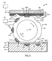
- FIG. 9 schematically illustrates a cross-sectional side view of another embodiment of a microelectronic device transport system.
- system 900 is a system similar to system 100 in that it is capable of massively parallel placement of microelectronic devices on a variety of substances.
- system 900 is capable of picking up and transporting a plurality of microelectronic devices from one substrate and placing them on another substrate for further processing.
- system 900 transports the microelectronic devices such that their contact surfaces align with pre-patterned insulating and conducting regions formed on the receiving substrate.
- system 900 transports the plurality of microelectronic devices using a “printing-like” technique.
- system 900 may be configured to “print” (or place) the microelectronic devices simultaneously onto a desired substrate.
- system 900 may include a roller assembly 902 , which is positioned between a carrier substrate 904 and a receiving substrate 906 .
- Roller assembly 902 may include roller 908 which is substantially similar to roller 108 described in reference to FIG. 1 .
- roller 908 may be a metal (e.g. steel) or rubber cylinder which can be engraved or otherwise machined to include a desired pattern along its outer surface. The pattern allows for roller 908 to pick up microelectronic devices and “print” the devices onto another surface.
- roller 908 may be assembled within system 900 such that it can rotate around a central axis 910 .
- central axis 910 may be a fixed axis such that roller 908 remains in the same lateral position while rotating.
- roller 908 may rotate about axis 910 in a clockwise direction as illustrated by arrow 912 .
- Roller 908 may, however, be movable in a vertical direction to allow for vertical positioning of roller 908 within system 900 .
- roller 908 may be fixed in both a lateral and a vertical direction, or movable in one or both directions.
- Rotation of roller 908 may be driven by an actuating mechanism 944 , such as, for example, a motor assembly or any similar actuating mechanism capable of driving rotation of an associated roller.
- Roller 908 may be positioned between carrier substrate 904 and receiving substrate 906 and include device openings 914 A, 914 B, 914 C, 914 D, 914 E, 914 F and 914 G along its outer surface.
- Device openings 914 A, 914 B, 914 C, 914 D, 914 E, 914 F and 914 G may be dimensioned to receive microelectronic devices 916 A, 916 B, 916 C, 916 D, 916 E, 916 F and 916 G, respectively.
- microelectronic devices 116 A- 116 G are photovoltaic solar cells
- device openings 914 A- 914 G may be recessed regions within the surface of roller 908 which have a similar shape to photovoltaic solar cells such that the cells can be received therein.
- microelectronic device 916 G is a multilayer photovoltaic solar cell including a substrate layer 918 , an insulator 920 formed on the substrate layer 918 and contact pads 922 A, 922 B and 922 C formed on the substrate layer 918 and insulator 920 .
- the remaining microelectronic devices 916 A- 916 F may have similar features.
- Device openings 914 A- 914 G may therefore have a size and shape matching the profile of each of the multilayered microelectronic devices 916 A- 916 G.
- the device openings 914 A- 914 G have a size and shape to match a profile of substrate layer 918 (e.g. a substantially rectangular profile).
- Device openings 914 A- 914 G may, however, have a size and shape similar to, and capable of receiving, other types of microelectronic devices, for example, a detector device, an integrated circuit device or the like.
- Device openings 914 A- 914 G may be formed within a surface of roller 908 according to any conventional processing technique capable of forming micro-scale recesses within a surface of roller 908 , for example, machining, laser imprinting, engraving, patterning, etching, or the like. It is further to be understood that although 7 device openings 914 A- 914 G are illustrated, any number of device openings, and in any desired spacing, may be formed around the outer surface of roller 908 .
- roller 908 is an elongated cylinder similar to roller 108 described in reference to FIG. 1 and FIG. 2 such that it includes multiple device openings along its length.
- roller 908 may include an array of device openings, including openings 914 A- 914 G, positioned around the circumference of roller 908 and extending along its length from one end to the other.
- any number and arrangement of device openings may be formed in roller 908 .
- the number and/or arrangement of device openings may be determined based on the desired number and/or arrangement of microelectronic devices on the receiving substrate.
- roller 908 may have device openings which match the desired pattern and therefore pick up the microelectronic devices and distribute them in the desired pattern on the receiving substrate.
- the number and/or arrangement of device openings is only constrained by the number of microelectronic devices desired to be picked up and transported by roller 908 .
- additional microelectronic devices similar to microelectronic devices 916 A- 916 G may be dispersed along the entire length and width of carrier substrate 904 such that they are spread out along the length of roller 908 and can be received by any of the device openings they may come in contact with.
- Carrier substrate 904 may be substantially similar to carrier substrate 104 described in reference to FIG. 1 .
- carrier substrate 904 is formed by a first fluid layer 932 and a second fluid layer 922 held within basin 924 .
- First fluid layer 932 and second fluid layer 922 may be made of any types of fluids which are immiscible with respect to one another such that one layer remains separate from the other.
- first fluid layer 932 may be made of a material which forms a base fluid layer and second fluid layer 922 may be a material which forms a fluid layer on top of first fluid layer 932 .
- first fluid layer 932 and second fluid layer 922 may include materials having different densities, for example, first fluid layer 932 may be water and second fluid layer 922 may be oil. In some embodiments, first fluid layer 932 is more dense than second fluid layer 922 .
- the only constraint of the specific materials selected for each of fluid layers 920 , 922 is that the material be one which is compatible with the microelectronic devices that may be aligned therein and one that will not impact any subsequent processing steps.
- first fluid layer 932 is water and second fluid layer 922 is toluene or oil.
- substrate layer 918 is hydrophilic, substrate layer 918 aligns with boundary 950 and faces roller 108 .
- Other materials may, however, be used to achieve such alignment.
- microelectronic devices 916 A- 916 G may initially be deposited onto carrier substrate 904 from the substrate on which they are formed by any standard release technique.
- microelectronic devices 916 A- 916 G may be formed as an array of microelectronic devices on a substrate. Once formed, microelectronic devices 916 A- 916 G may be transferred from the substrate on which they are formed to carrier substrate 904 by releasing them from the substrate using, for example, a chemical release process such as etching or a mechanical separation.
- microelectronic devices 916 A- 916 G may be held onto the substrate by an adhesive or the like which will dissolve or otherwise release microelectronic devices 916 A- 916 G into carrier substrate 904 once submerged within first fluid layer 932 and/or second fluid layer 922 .
- microelectronic devices 916 A- 916 C are deposited into carrier substrate 904 by simply submerging the microelectronic devices 916 A- 916 G and associated substrate into first fluid layer 932 and/or second fluid layer 922 . Once released into first fluid layer 932 and second fluid layer 922 , microelectronic devices 916 A- 916 G will orient themselves in the desired manner as previously discussed.
- microelectronic devices 916 A- 916 G may be singular devices which are already free floating within a carrier fluid. In this case, microelectronic devices 916 A- 916 G may be picked and placed into carrier substrate 904 or dumped into carrier substrate 904 from the carrier fluid.
- Carrier substrate 904 is further configured such that it is laterally translatable and can move the microelectronic devices positioned therein toward roller 908 .
- first fluid layer 932 and second fluid layer 922 may flow in a direction of roller 908 as illustrated by arrows 926 .
- the fluid within the first fluid layer 932 and the second fluid layer 922 may be caused to flow by, for example, a pump, stirring bar or other mechanism capable of generating a current in the desired direction (e.g. in the direction of arrows 926 A and 926 B).
- microelectronic devices 916 A- 916 G are continuously drawn toward and under roller 908 such that as roller 908 rotates, microelectronic devices 916 A- 916 G become aligned within an open device opening (e.g. device opening 914 A). Once aligned, one or more of the microelectronic devices (e.g. microelectronic device 916 B) are drawn into a device opening (e.g. device opening 914 B) and remain attached to roller 908 as roller 908 rotates about axis 910 . Attachment of the microelectronic devices within the respective device opening may be achieved by any suitable mechanism.
- frictional forces, electrostatic forces, capillary forces, vacuum forces, adhesive forces, or the like may provide the force used to hold the devices within the desired openings.
- one or more of the device openings may include channels, which are formed during formation of the openings (e.g. etching) and are coupled to a vacuum source such that a vacuum force capable of drawing devices into the openings can be created.
- receiving substrate 906 can be any type of receiving surface where microelectronic devices 916 A- 916 G are desired to be deposited.
- receiving substrate 906 could be a final assembly substrate where microelectronic devices will remain once deposited, or receiving substrate 906 could be a carrier substrate that receives microelectronic devices 916 A- 916 G prior to depositing them onto a further receiving substrate.
- Microelectronic devices 916 A- 916 G are released onto receiving substrate 906 once they reach the top of roller 908 as illustrated in FIG. 9 .
- receiving substrate 906 is laterally translatable in a direction away from roller 908 , as illustrated by arrow 928 .
- the direction of movement of receiving substrate 906 may, in some embodiments, be opposite that of carrier substrate 904 . Movement of receiving substrate 906 may be driven by for example, an actuating mechanism 942 , such as, for example, a conveyor belt assembly or any similar actuating mechanism capable of moving a substrate positioned thereon in the desired direction.
- receiving substrate 906 includes a patterned layer 938 formed on receiving substrate 906 , which is pre-patterned to have patterned openings 940 A, 940 B and 940 C in a shape of microelectronic devices 916 A- 916 G.
- patterned layer 938 is a multilayered structure having alternating insulating and conductive layers.
- receiving substrate 906 may include conductive layer 930 formed on receiving substrate 906 , insulating layer 932 formed on conductive layer 930 , conductive layer 934 formed on insulating layer 932 and insulating layer 936 formed on conductive layer 936 .
- Patterned layer 938 may be patterned such that patterned openings 940 A, 940 B and 940 C have a similar shape and profile as the contact side of microelectronic devices 916 A- 916 G.
- patterned openings 940 A, 940 B and 940 C may be patterned to have a stepped pattern such that conductive layer 934 aligns with contact pads 922 A, 922 C and conductive layer 930 aligns with contact pad 922 B.
- conductive layers 930 and 934 may be used to separately connect contact pads 922 A, 922 C and 922 B to a desired device (e.g. another microelectronic device or other circuitry for transfer of power or data).
- Patterning of openings 940 A- 940 C may be achieved according to any known microelectronic device processing technique capable of forming micro-scale recesses (e.g. 1 mm or less) within a substrate, for example, machining, laser imprinting, engraving, patterning, etching, or the like.
- microelectronic devices 916 A- 916 C may then remain attached to receiving substrate 906 for electrical connection to other devices, or subsequently removed and transported to a final receiving surface.
- FIG. 10 schematically illustrates a cross-sectional side view of another embodiment of a microelectronic device. Similar to the previously discussed microelectronic devices 116 A- 116 G and 916 A- 916 G, microelectronic device 1000 is a multilayered device, except in this embodiment, microelectronic device 1000 includes a second semiconductor layer having an additional contact pad. Representatively, microelectronic device 1000 may be a photovoltaic cell of a multi-junction cell type which can receive light input from two sides.
- microelectronic device 1000 may include a first substrate layer 1002 A surrounded by a first insulating layer 1004 A and a second substrate layer 1002 B surrounded by a second insulating layer 1004 B, with the second substrate layer 1002 B being stacked on top of the first substrate layer 1002 A.
- First substrate layer 1002 A may include a contact pad 1006 surrounded by an insulating layer 1008 and another contact pad 1010 .
- Each of contact pads 1006 and 1010 may be connected to junction regions 1014 and 1012 , respectively.
- Second substrate layer 1002 B may further include contact pad 1016 surrounded by insulating layer 1018 and contact pad 1020 .
- Each of contact pads 1016 and 1020 may be connected to junction regions 1024 and 1022 , respectively.
- microelectronic device 1000 may receive light input from both substrate sides. It is further to be understood that, although not illustrated, any of the previously discussed transport systems 100 and 900 may be configured to transport multi-junction cell type of device 1000 . In such cases, the only difference between systems 100 and 900 would be that the device openings and patterned openings would be shaped and sized to conform to the multi leveled structure of device 1000 .
- a carrier substrate is described as including fluid layers, it is further contemplated that the carrier substrate may be made of any material(s) capable of carrying and transporting the microelectronic devices as described herein.
- the carrier substrate may be made of a single fluid layer or a solid laterally translatable substrate material that can transport microelectronic devices in a direction of the roller assembly as previously discussed.
- microelectronic devices such as PV cells are described herein, other types of devices are contemplated, including, but are not limited to, DIACs, diodes (rectifier diode), gunn diodes, IMPATT diodes, laser diodes, light-emitting diodes (LED), photocells, PIN diodes, schottky diodes, tunnel diodes, VCSELs, VECSELs, zener diodes, bipolar transistors, darlington transistors, field-effect transistors, insulated-gate bipolar transistor (IGBT)s, silicon controlled rectifiers, thyristors, TRIACs, unijunction transistors, hall effect sensors (magnetic field sensor), integrated circuits (ICs), charge-coupled devices (CCD), microprocessor devices, random-access memory (RAM) devices, or read-only memory (ROM) devices.
- DIACs diodes (rectifier diode), gunn diodes, IMPATT diodes, laser diodes,
Landscapes
- Engineering & Computer Science (AREA)
- Manufacturing & Machinery (AREA)
- Microelectronics & Electronic Packaging (AREA)
- Mechanical Engineering (AREA)
- Container, Conveyance, Adherence, Positioning, Of Wafer (AREA)
- Life Sciences & Earth Sciences (AREA)
- Sustainable Development (AREA)
- Sustainable Energy (AREA)
- Photovoltaic Devices (AREA)
Abstract
Description
Claims (7)
Priority Applications (2)
| Application Number | Priority Date | Filing Date | Title |
|---|---|---|---|
| US14/088,725 US9763370B2 (en) | 2013-03-15 | 2013-11-25 | Apparatus for assembly of microelectronic devices |
| PCT/US2014/027508 WO2014152592A1 (en) | 2013-03-15 | 2014-03-14 | Printed crystalline microelectronic devices |
Applications Claiming Priority (2)
| Application Number | Priority Date | Filing Date | Title |
|---|---|---|---|
| US201361791143P | 2013-03-15 | 2013-03-15 | |
| US14/088,725 US9763370B2 (en) | 2013-03-15 | 2013-11-25 | Apparatus for assembly of microelectronic devices |
Publications (2)
| Publication Number | Publication Date |
|---|---|
| US20140259633A1 US20140259633A1 (en) | 2014-09-18 |
| US9763370B2 true US9763370B2 (en) | 2017-09-12 |
Family
ID=51520626
Family Applications (1)
| Application Number | Title | Priority Date | Filing Date |
|---|---|---|---|
| US14/088,725 Active 2034-07-09 US9763370B2 (en) | 2013-03-15 | 2013-11-25 | Apparatus for assembly of microelectronic devices |
Country Status (2)
| Country | Link |
|---|---|
| US (1) | US9763370B2 (en) |
| WO (1) | WO2014152592A1 (en) |
Families Citing this family (7)
| Publication number | Priority date | Publication date | Assignee | Title |
|---|---|---|---|---|
| KR102066896B1 (en) * | 2016-04-14 | 2020-01-16 | 가부시키가이샤 무라타 세이사쿠쇼 | Method for manufacturing a conveying device for measuring the characteristics of electronic parts and receiving member for measuring the characteristics of electronic parts |
| DE102016115186A1 (en) * | 2016-08-16 | 2018-02-22 | Osram Opto Semiconductors Gmbh | Method for mounting semiconductor chips and device for transferring semiconductor chips |
| US10317256B2 (en) | 2017-04-14 | 2019-06-11 | Palo Alto Research Center Incorporated | Monitoring transportation systems |
| US10604843B2 (en) * | 2017-05-10 | 2020-03-31 | Xerox Corporation | High registration particles-transferring system |
| GB2563600B (en) * | 2017-06-19 | 2022-05-11 | Pragmatic Printing Ltd | Apparatus and method for manufacturing plurality of electronic circuits |
| JP2020025064A (en) * | 2018-07-31 | 2020-02-13 | アルディーテック株式会社 | Manufacturing method of light emitting device integrated device and light emitting device array device |
| US12550654B2 (en) * | 2020-08-21 | 2026-02-10 | Advanced Semiconductor Engineering, Inc. | Method for manufacturing semiconductor package |
Citations (14)
| Publication number | Priority date | Publication date | Assignee | Title |
|---|---|---|---|---|
| US5191834A (en) | 1988-10-14 | 1993-03-09 | Man Roland Druckmaschinen Ag | Printing system with printing form having a ferro-electric layer |
| US6364089B1 (en) * | 1999-12-10 | 2002-04-02 | National Semiconductor Corporation | Multi-station rotary die handling device |
| US6555408B1 (en) * | 1999-02-05 | 2003-04-29 | Alien Technology Corporation | Methods for transferring elements from a template to a substrate |
| US20030140485A1 (en) * | 2001-03-30 | 2003-07-31 | Osamu Yamazaki | Semiconductor chip carrying adhesive tape/sheet, semiconductor chip carrier, semiconductor chip mounting method and semiconductor chip packaging body |
| WO2004004025A2 (en) | 2002-06-28 | 2004-01-08 | Infineon Technologies Ag | Method for the economical structuring of conducting polymers by means of defining hydrophilic and hydrophobic regions |
| US20040154161A1 (en) * | 2003-02-07 | 2004-08-12 | Hallys Corporation | Random-period chip transfer apparatus |
| US6855378B1 (en) | 1998-08-21 | 2005-02-15 | Sri International | Printing of electronic circuits and components |
| US6932136B1 (en) * | 2004-04-08 | 2005-08-23 | National Semiconductor Corporation | Post singulation die separation apparatus and method for bulk feeding operation |
| JP2005335755A (en) * | 2004-05-26 | 2005-12-08 | Iwata Label Co Ltd | RFID label sticking method and sticking apparatus |
| US20060072295A1 (en) | 2003-01-17 | 2006-04-06 | Reiner Gotzen | Method for producing microsystems |
| US20080023296A1 (en) | 2004-09-22 | 2008-01-31 | Hallys Corporation | Transfer Apparatus |
| US20080222876A1 (en) * | 2007-03-12 | 2008-09-18 | Tyco Electronics Corporation | System for attaching electronic components to molded interconnection devices |
| US20100018049A1 (en) | 2000-02-25 | 2010-01-28 | Ibiden Co., Ltd. | Multilayer printed circuit board and multilayer printed circuit board manufacturing method |
| US20120321793A1 (en) | 2010-02-19 | 2012-12-20 | Axel Lundvall | Method for printing product features on a substrate sheet |
-
2013
- 2013-11-25 US US14/088,725 patent/US9763370B2/en active Active
-
2014
- 2014-03-14 WO PCT/US2014/027508 patent/WO2014152592A1/en not_active Ceased
Patent Citations (14)
| Publication number | Priority date | Publication date | Assignee | Title |
|---|---|---|---|---|
| US5191834A (en) | 1988-10-14 | 1993-03-09 | Man Roland Druckmaschinen Ag | Printing system with printing form having a ferro-electric layer |
| US6855378B1 (en) | 1998-08-21 | 2005-02-15 | Sri International | Printing of electronic circuits and components |
| US6555408B1 (en) * | 1999-02-05 | 2003-04-29 | Alien Technology Corporation | Methods for transferring elements from a template to a substrate |
| US6364089B1 (en) * | 1999-12-10 | 2002-04-02 | National Semiconductor Corporation | Multi-station rotary die handling device |
| US20100018049A1 (en) | 2000-02-25 | 2010-01-28 | Ibiden Co., Ltd. | Multilayer printed circuit board and multilayer printed circuit board manufacturing method |
| US20030140485A1 (en) * | 2001-03-30 | 2003-07-31 | Osamu Yamazaki | Semiconductor chip carrying adhesive tape/sheet, semiconductor chip carrier, semiconductor chip mounting method and semiconductor chip packaging body |
| WO2004004025A2 (en) | 2002-06-28 | 2004-01-08 | Infineon Technologies Ag | Method for the economical structuring of conducting polymers by means of defining hydrophilic and hydrophobic regions |
| US20060072295A1 (en) | 2003-01-17 | 2006-04-06 | Reiner Gotzen | Method for producing microsystems |
| US20040154161A1 (en) * | 2003-02-07 | 2004-08-12 | Hallys Corporation | Random-period chip transfer apparatus |
| US6932136B1 (en) * | 2004-04-08 | 2005-08-23 | National Semiconductor Corporation | Post singulation die separation apparatus and method for bulk feeding operation |
| JP2005335755A (en) * | 2004-05-26 | 2005-12-08 | Iwata Label Co Ltd | RFID label sticking method and sticking apparatus |
| US20080023296A1 (en) | 2004-09-22 | 2008-01-31 | Hallys Corporation | Transfer Apparatus |
| US20080222876A1 (en) * | 2007-03-12 | 2008-09-18 | Tyco Electronics Corporation | System for attaching electronic components to molded interconnection devices |
| US20120321793A1 (en) | 2010-02-19 | 2012-12-20 | Axel Lundvall | Method for printing product features on a substrate sheet |
Non-Patent Citations (1)
| Title |
|---|
| International Search Report and Written Opinion for PCT/US2014/027508, dated Jul. 15, 2014. |
Also Published As
| Publication number | Publication date |
|---|---|
| US20140259633A1 (en) | 2014-09-18 |
| WO2014152592A1 (en) | 2014-09-25 |
Similar Documents
| Publication | Publication Date | Title |
|---|---|---|
| US9763370B2 (en) | Apparatus for assembly of microelectronic devices | |
| US20240170430A1 (en) | Chiplets with connection posts | |
| US10222698B2 (en) | Chiplets with wicking posts | |
| US10262966B2 (en) | Methods for surface attachment of flipped active components | |
| KR101681437B1 (en) | Chip support substrate, method for supporting chip, three-dimensional integrated circuit, assembly device, and method for manufacturing three-dimensional integrated circuit | |
| US11064609B2 (en) | Printable 3D electronic structure | |
| EP3420582B1 (en) | Efficiently micro-transfer printing micro-scale devices onto large-format substrates | |
| US6780696B1 (en) | Method and apparatus for self-assembly of functional blocks on a substrate facilitated by electrode pairs | |
| CN103563082B (en) | Photovoltaic device and manufacture method thereof | |
| US20230091571A1 (en) | Methods of making printed structures | |
| CN103390601A (en) | Chip package and method for forming the same | |
| WO2015193433A4 (en) | Micro assembled high frequency devices and arrays and method of making the same | |
| KR20070006885A (en) | Apparatus and method for transporting conductive components during semiconductor device manufacturing | |
| WO2017162913A1 (en) | A quantum dot photodetector apparatus and associated methods | |
| US10431561B2 (en) | Pre-conductive array disposed on target circuit substrate and conductive structure array thereof | |
| US20070231826A1 (en) | Article and assembly for magnetically directed self assembly | |
| US10854566B2 (en) | Pre-conductive array disposed on target circuit substrate and conductive structure array thereof | |
| EP4657523A1 (en) | Additive manufacturing of fan-out packages | |
| KR102708514B1 (en) | Apparatus of rotary type for transferring cell-jig, apparatus for tabbing including the same, and method for transferring cell-jig | |
| US20240014063A1 (en) | Method of manufacturing a semiconductor device | |
| CN114616687A (en) | Optoelectronic component and method for contacting an optoelectronic component | |
| US20140261616A1 (en) | Spreading devices into a 2-d module layout |
Legal Events
| Date | Code | Title | Description |
|---|---|---|---|
| AS | Assignment |
Owner name: SANDIA CORPORATION, NEW MEXICO Free format text: ASSIGNMENT OF ASSIGNORS INTEREST;ASSIGNORS:OKANDAN, MURAT;NIELSON, GREGORY N.;CRUZ-CAMPA, JOSE LUIS;AND OTHERS;SIGNING DATES FROM 20140207 TO 20140407;REEL/FRAME:032871/0098 |
|
| AS | Assignment |
Owner name: U.S. DEPARTMENT OF ENERGY, DISTRICT OF COLUMBIA Free format text: CONFIRMATORY LICENSE;ASSIGNOR:SANDIA CORPORATION;REEL/FRAME:034990/0165 Effective date: 20140109 |
|
| AS | Assignment |
Owner name: NATIONAL TECHNOLOGY & ENGINEERING SOLUTIONS OF SAN Free format text: CHANGE OF NAME;ASSIGNOR:SANDIA CORPORATION;REEL/FRAME:043477/0836 Effective date: 20170501 |
|
| AS | Assignment |
Owner name: NATIONAL TECHNOLOGY & ENGINEERING SOLUTIONS OF SAN Free format text: CHANGE OF NAME;ASSIGNOR:SANDIA CORPORATION;REEL/FRAME:043481/0132 Effective date: 20170501 |
|
| STCF | Information on status: patent grant |
Free format text: PATENTED CASE |
|
| MAFP | Maintenance fee payment |
Free format text: PAYMENT OF MAINTENANCE FEE, 4TH YEAR, LARGE ENTITY (ORIGINAL EVENT CODE: M1551); ENTITY STATUS OF PATENT OWNER: LARGE ENTITY Year of fee payment: 4 |
|
| MAFP | Maintenance fee payment |
Free format text: PAYMENT OF MAINTENANCE FEE, 8TH YEAR, LARGE ENTITY (ORIGINAL EVENT CODE: M1552); ENTITY STATUS OF PATENT OWNER: LARGE ENTITY Year of fee payment: 8 |