US9761440B2 - Surface passivation on indium-based materials - Google Patents
Surface passivation on indium-based materials Download PDFInfo
- Publication number
- US9761440B2 US9761440B2 US14/658,012 US201514658012A US9761440B2 US 9761440 B2 US9761440 B2 US 9761440B2 US 201514658012 A US201514658012 A US 201514658012A US 9761440 B2 US9761440 B2 US 9761440B2
- Authority
- US
- United States
- Prior art keywords
- layer
- semiconductor
- indium
- sulfide
- forming
- Prior art date
- Legal status (The legal status is an assumption and is not a legal conclusion. Google has not performed a legal analysis and makes no representation as to the accuracy of the status listed.)
- Expired - Fee Related, expires
Links
Images


Classifications
-
- H—ELECTRICITY
- H01—ELECTRIC ELEMENTS
- H01L—SEMICONDUCTOR DEVICES NOT COVERED BY CLASS H10
- H01L21/00—Processes or apparatus adapted for the manufacture or treatment of semiconductor or solid state devices or of parts thereof
- H01L21/02—Manufacture or treatment of semiconductor devices or of parts thereof
- H01L21/02104—Forming layers
- H01L21/02107—Forming insulating materials on a substrate
- H01L21/02225—Forming insulating materials on a substrate characterised by the process for the formation of the insulating layer
- H01L21/02227—Forming insulating materials on a substrate characterised by the process for the formation of the insulating layer formation by a process other than a deposition process
-
- H10P14/6302—
-
- H—ELECTRICITY
- H01—ELECTRIC ELEMENTS
- H01L—SEMICONDUCTOR DEVICES NOT COVERED BY CLASS H10
- H01L21/00—Processes or apparatus adapted for the manufacture or treatment of semiconductor or solid state devices or of parts thereof
- H01L21/02—Manufacture or treatment of semiconductor devices or of parts thereof
- H01L21/02104—Forming layers
- H01L21/02107—Forming insulating materials on a substrate
- H01L21/02109—Forming insulating materials on a substrate characterised by the type of layer, e.g. type of material, porous/non-porous, pre-cursors, mixtures or laminates
- H01L21/02112—Forming insulating materials on a substrate characterised by the type of layer, e.g. type of material, porous/non-porous, pre-cursors, mixtures or laminates characterised by the material of the layer
- H01L21/02172—Forming insulating materials on a substrate characterised by the type of layer, e.g. type of material, porous/non-porous, pre-cursors, mixtures or laminates characterised by the material of the layer the material containing at least one metal element, e.g. metal oxides, metal nitrides, metal oxynitrides or metal carbides
- H01L21/02175—Forming insulating materials on a substrate characterised by the type of layer, e.g. type of material, porous/non-porous, pre-cursors, mixtures or laminates characterised by the material of the layer the material containing at least one metal element, e.g. metal oxides, metal nitrides, metal oxynitrides or metal carbides characterised by the metal
-
- H—ELECTRICITY
- H01—ELECTRIC ELEMENTS
- H01L—SEMICONDUCTOR DEVICES NOT COVERED BY CLASS H10
- H01L21/00—Processes or apparatus adapted for the manufacture or treatment of semiconductor or solid state devices or of parts thereof
- H01L21/02—Manufacture or treatment of semiconductor devices or of parts thereof
- H01L21/02104—Forming layers
- H01L21/02107—Forming insulating materials on a substrate
- H01L21/02225—Forming insulating materials on a substrate characterised by the process for the formation of the insulating layer
- H01L21/02227—Forming insulating materials on a substrate characterised by the process for the formation of the insulating layer formation by a process other than a deposition process
- H01L21/0223—Forming insulating materials on a substrate characterised by the process for the formation of the insulating layer formation by a process other than a deposition process formation by oxidation, e.g. oxidation of the substrate
- H01L21/02233—Forming insulating materials on a substrate characterised by the process for the formation of the insulating layer formation by a process other than a deposition process formation by oxidation, e.g. oxidation of the substrate of the semiconductor substrate or a semiconductor layer
- H01L21/02241—III-V semiconductor
-
- H—ELECTRICITY
- H01—ELECTRIC ELEMENTS
- H01L—SEMICONDUCTOR DEVICES NOT COVERED BY CLASS H10
- H01L23/00—Details of semiconductor or other solid state devices
- H01L23/28—Encapsulations, e.g. encapsulating layers, coatings, e.g. for protection
- H01L23/29—Encapsulations, e.g. encapsulating layers, coatings, e.g. for protection characterised by the material, e.g. carbon
- H01L23/291—Oxides or nitrides or carbides, e.g. ceramics, glass
-
- H—ELECTRICITY
- H01—ELECTRIC ELEMENTS
- H01L—SEMICONDUCTOR DEVICES NOT COVERED BY CLASS H10
- H01L23/00—Details of semiconductor or other solid state devices
- H01L23/28—Encapsulations, e.g. encapsulating layers, coatings, e.g. for protection
- H01L23/31—Encapsulations, e.g. encapsulating layers, coatings, e.g. for protection characterised by the arrangement or shape
- H01L23/3157—Partial encapsulation or coating
- H01L23/3171—Partial encapsulation or coating the coating being directly applied to the semiconductor body, e.g. passivation layer
-
- H01L29/20—
-
- H01L29/452—
-
- H01L29/513—
-
- H01L29/66522—
-
- H01L29/78—
-
- H—ELECTRICITY
- H10—SEMICONDUCTOR DEVICES; ELECTRIC SOLID-STATE DEVICES NOT OTHERWISE PROVIDED FOR
- H10D—INORGANIC ELECTRIC SEMICONDUCTOR DEVICES
- H10D30/00—Field-effect transistors [FET]
- H10D30/01—Manufacture or treatment
- H10D30/021—Manufacture or treatment of FETs having insulated gates [IGFET]
- H10D30/024—Manufacture or treatment of FETs having insulated gates [IGFET] of fin field-effect transistors [FinFET]
-
- H—ELECTRICITY
- H10—SEMICONDUCTOR DEVICES; ELECTRIC SOLID-STATE DEVICES NOT OTHERWISE PROVIDED FOR
- H10D—INORGANIC ELECTRIC SEMICONDUCTOR DEVICES
- H10D30/00—Field-effect transistors [FET]
- H10D30/60—Insulated-gate field-effect transistors [IGFET]
-
- H—ELECTRICITY
- H10—SEMICONDUCTOR DEVICES; ELECTRIC SOLID-STATE DEVICES NOT OTHERWISE PROVIDED FOR
- H10D—INORGANIC ELECTRIC SEMICONDUCTOR DEVICES
- H10D30/00—Field-effect transistors [FET]
- H10D30/60—Insulated-gate field-effect transistors [IGFET]
- H10D30/62—Fin field-effect transistors [FinFET]
-
- H—ELECTRICITY
- H10—SEMICONDUCTOR DEVICES; ELECTRIC SOLID-STATE DEVICES NOT OTHERWISE PROVIDED FOR
- H10D—INORGANIC ELECTRIC SEMICONDUCTOR DEVICES
- H10D30/00—Field-effect transistors [FET]
- H10D30/60—Insulated-gate field-effect transistors [IGFET]
- H10D30/751—Insulated-gate field-effect transistors [IGFET] having composition variations in the channel regions
-
- H—ELECTRICITY
- H10—SEMICONDUCTOR DEVICES; ELECTRIC SOLID-STATE DEVICES NOT OTHERWISE PROVIDED FOR
- H10D—INORGANIC ELECTRIC SEMICONDUCTOR DEVICES
- H10D62/00—Semiconductor bodies, or regions thereof, of devices having potential barriers
- H10D62/80—Semiconductor bodies, or regions thereof, of devices having potential barriers characterised by the materials
- H10D62/85—Semiconductor bodies, or regions thereof, of devices having potential barriers characterised by the materials being Group III-V materials, e.g. GaAs
-
- H10D64/01358—
-
- H—ELECTRICITY
- H10—SEMICONDUCTOR DEVICES; ELECTRIC SOLID-STATE DEVICES NOT OTHERWISE PROVIDED FOR
- H10D—INORGANIC ELECTRIC SEMICONDUCTOR DEVICES
- H10D64/00—Electrodes of devices having potential barriers
- H10D64/60—Electrodes characterised by their materials
- H10D64/62—Electrodes ohmically coupled to a semiconductor
-
- H—ELECTRICITY
- H10—SEMICONDUCTOR DEVICES; ELECTRIC SOLID-STATE DEVICES NOT OTHERWISE PROVIDED FOR
- H10D—INORGANIC ELECTRIC SEMICONDUCTOR DEVICES
- H10D64/00—Electrodes of devices having potential barriers
- H10D64/60—Electrodes characterised by their materials
- H10D64/66—Electrodes having a conductor capacitively coupled to a semiconductor by an insulator, e.g. MIS electrodes
- H10D64/68—Electrodes having a conductor capacitively coupled to a semiconductor by an insulator, e.g. MIS electrodes characterised by the insulator, e.g. by the gate insulator
- H10D64/681—Electrodes having a conductor capacitively coupled to a semiconductor by an insulator, e.g. MIS electrodes characterised by the insulator, e.g. by the gate insulator having a compositional variation, e.g. multilayered
- H10D64/685—Electrodes having a conductor capacitively coupled to a semiconductor by an insulator, e.g. MIS electrodes characterised by the insulator, e.g. by the gate insulator having a compositional variation, e.g. multilayered being perpendicular to the channel plane
-
- H10P14/6312—
-
- H10P14/6939—
-
- H10P50/00—
-
- H10P70/15—
-
- H10P70/20—
-
- H10W74/137—
-
- H10W74/43—
Definitions
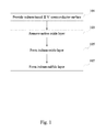
- FIG. 1 shows a flow chart to illustrate a method making a semiconductor structure constructed according to various aspects of the present disclosure in accordance with some embodiments.
- FIG. 2 shows illustrative figures that correspond to the method described in FIG. 1 in accordance with various embodiments.
- FIGS. 3A-3C shows an example of a semiconductor feature that includes a passivation layer in accordance with some embodiments.
- FIGS. 4A-4C show another example of a semiconductor feature that includes a passivation layer in accordance with some embodiments.
- FIGS. 5A and 5B shows an effect of different pre-clean solutions and/or different wet oxidation solutions on a formed indium-sulfide layer and a passivated In-based semiconductor surface in accordance with some embodiments.
- first and second features are formed in direct contact
- additional features may be formed interposing the first and second features, such that the first and second features may not be in direct contact.
- the present disclosure is generally directed to a semiconductor device, and more particularly to a semiconductor device having an indium (In)-based material III-V compound semiconductor surface. It is an objective of the present disclosure to provide a method for effectively passivating such an In-based semiconductor surface while providing sufficient process windows and a more compatible fabrication condition for semiconductor device fabrications.
- the In-based III-V compound semiconductor surface may include materials such as InAs, InP, InSb, InN, In x Ga 1-x As, In x Al 1-x As, In x Ga 1-x N, In x Ga 1-x P, and/or In x As 1-x Sb y P 1-y , where “x”, “1-x”, “y”, and “1-y” are the proportions of the corresponding materials.
- x is the proportion of InAs and “1-x” is the proportion of GaAs.
- all the proportions e.g., x, 1-x, y, 1-y
- the disclosed method is described to be implemented on passivating surfaces of In-based materials, the method may be generalized to be used on other types of semiconductor materials, such as Si, Ge, Si-based semiconductor materials and/or Ge-based semiconductor materials.
- FIG. 1 a flow chart of a method 100 of forming a passivation layer by a sulfurization process on a semiconductor surface in accordance with some illustrative embodiments.
- the method 100 is merely an example, and is not intended to limit the present disclosure. Additional operations can be provided before, during, and after the method 100 , and some operations described can be replaced, eliminated, or moved around for additional embodiments of the method.
- the method 100 starts in block 101 with providing a semiconductor surface that includes indium (In)-based III-V compound semiconductor material.
- In-based III-V compound semiconductor materials include InAs, InP, InSb, InN, InGaAs, InAlAs, InAlP, InGaN, InGaP, and/or InAsSbP.
- the In-based semiconductor surface to be passivated by the disclosed method may be formed by any suitable manner, such as by epitaxial growth or deposition, or provided as an exposed surface of a bulk structure, a semiconductor feature, or material.
- the method 100 continues in block 103 with removing contaminants, including native oxides, contaminant films, particulate matter, and/or other types of contaminants, which may be formed on the In-based semiconductor surface.
- the contaminant such as a native oxide layer
- HCl hydrogen chloride
- the In-based semiconductor surface may be deposited using a UHV (ultra-high vacuum) MBE (molecular beam epitaxy) tool and remains within the tool. Because the semiconductor surface is maintained within a vacuum, in this particular embodiment, the surface may remain relatively uncontaminated.
- the operation in block 103 may be optional.
- the method 100 continues in block 105 with forming an indium-oxide layer over the In-based semiconductor surface.
- the formation of the indium-oxide layer is performed via a wet oxidation process. More particularly, the wet oxidation process may include exposing the In-based semiconductor surface to an ammonia-peroxide mixture (APM, or NH 4 OH+H 2 O 2 ).
- APM ammonia-peroxide mixture
- an indium-oxide (In 2 O 3 ) layer may be formed on the InGaAs surface.
- the wet oxidation process may be performed at a temperature level ranging from 25° C. to 60° C. More specifically, in the wet oxidation process, APM may be applied in either a wet dipping process or a spin-coating type of process for a reaction time in a range from 10 seconds to 10 minutes. Still according to some embodiments, a thickness of the indium-oxide layer is based on a reaction time, temperature, and/or a concentration of NH 4 OH in APM. For example, with a longer reaction time and higher temperature, a thicker layer of indium-oxide may be formed over the In-based surface.
- the method 100 proceeds with forming an indium-sulfide layer over the In-based surface.
- the indium-sulfide layer is implemented via applying an aqueous solution of (NH 4 ) 2 S at a concentration between 0.1% by weight and 20% by weight on the formed indium-oxide layer formed in block 105 .
- Such (NH 4 ) 2 S may be applied to the indium-oxide layer to form the indium-sulfide layer on the In-based semiconductor surface in either a wet dipping process or a spin-coating type of process for a reaction time in a range from 10 seconds to 10 minutes and at a temperature level ranging from 25° C. to 80° C.
- the indium-sulfide layer may be formed via a series of chemical reactions, including ammonium sulfide dissociation, sulfication of indium-oxide layer, etc.
- ammonium sulfide dissociation may include:
- (NH 4 ) 2 S dissociation results in formation of sulfidation specie of HS ⁇ , (NH 4 ) 2 S ⁇ 2NH 4 + +S 2 ⁇ S 2 ⁇ +H 2 O ⁇ HS ⁇ +OH ⁇ , and the sulfidation of indium-oxide layer may include: It is thermodynamically favorable to replace the OH bonds of In(OH) 3 by the HS ⁇ , and form indium sulfide layer which is stable in the alkaline solution, 2In(OH) 3 +6HS ⁇ ⁇ 2In(HS) 3 +6OH ⁇ ⁇ In 2 S 3 +3H 2 S+6OH ⁇ .
- an indium-sulfide (i.e., In 2 S 3 ) layer is formed on the InGaAs surface.
- the indium-sulfide layer can be any desired thickness.
- at least three monolayers of indium-sulfide is preferably to be formed on the In-based surface.
- the thickness of the indium-sulfide layer may be determined by one or multiple factors, such as an initial thickness of the indium-oxide layer, reaction temperature and time of forming the indium-sulfide layer, concentration of APM, and concentration of the (NH 4 ) 2 S.
- the formation of the indium-sulfide layer on the In-based surface may be used as a passivation layer.
- a formation of native oxide on the In-based surface may be suppressed, and therefore may provide advantages to improve a quality of the In-based surface.
- an improved quality of a surface may be implemented by reducing a density of interface states (D it ) on the surface of the In-based semiconductor material.
- Such improvement of the In-based semiconductor surface may advantageously impact an integrated circuit as a whole.
- an improved surface on a source/drain features may advantageously reduce a contact resistance, and thus may provide an enhancement of a switching speed of an integrated circuit that utilizes such source/drain features.
- Block 201 corresponds to block 101 in FIG. 1 , wherein an In-based III-V semiconductor substrate 202 is provided.
- Block 203 corresponds to block 105 with forming an indium-oxide layer 204 over the In-based substrate 202 .
- block 205 corresponds to block 107 with forming an indium-sulfide layer 206 over the In-based substrate.
- the indium-oxide layer 204 in block 204 may be consumed completely to form the indium-sulfide layer 206 .
- the indium-oxide layer 204 may be transformed or sulfurized to the indium-sulfide layer 206 completely.
- the indium-oxide layer 204 may be consumed partially via the sulfurization operation, which means that after forming the indium-sulfide layer 206 , there may be left indium-oxide layer and newly formed indium-sulfide layer 206 existent over the In-based substrate 202 ,
- the method 100 described above is used in forming semiconductor devices 300 and 400 discussed below in FIGS. 3A-3C and 4A-4C .
- the devices 300 and 400 may be an intermediate device fabricated during processing of an IC, or a portion thereof, that may comprise SRAM and/or other logic circuits, passive components such as resistors, capacitors, and inductors, and active components such as p-type FETs (PFETs), n-type FETs (NFETs), FinFETs, metal-oxide semiconductor field effect transistors (MOSFET), gate-all-around (GAA) FETs, vertical FETs, complementary metal-oxide semiconductor (CMOS) transistors, bipolar transistors, high voltage transistors, high frequency transistors, other memory cells, and/or combinations thereof.
- PFETs p-type FETs
- NFETs n-type FETs
- MOSFET metal-oxide semiconductor field effect transistors
- GAA gate-all-around
- FIGS. 3A-3C show different stages to fabricate an exemplary semiconductor structure 300 that includes an indium-sulfide as a passivation layer in accordance with various embodiments.
- Semiconductor structure 300 includes a gate stack of a FinFET.
- such FinFET includes a fin as a channel region that is formed of indium-based III-V semiconductor material.
- Semiconductor structure 300 is merely an example to illustrate that the disclosed passivation layer (indium-sulfide layer) can be applied to whatever semiconductor structures, such as planer FET, nanowire FET, vertical FET, GAA FET, etc., that includes an In-based semiconductor surface.
- semiconductor structure 300 includes a semiconductor substrate 301 , a first semiconductor layer 305 formed of a first semiconductor material, an isolation feature 303 , and a fin structure 307 formed of a second semiconductor material.
- the semiconductor substrate 201 may be a bulk silicon substrate.
- the substrate 201 comprises an elementary semiconductor, such as silicon or germanium in a crystalline structure; a compound semiconductor, such as SiGe, SiC, GaAs, GaP, InP, InAs, and/or InSb; or combinations thereof.
- the substrate 201 includes a silicon-on-insulator (SOI) substrate.
- SOI substrate can be fabricated using separation by implantation of oxygen (SIMOX), wafer bonding, and/or other suitable methods.
- the substrate 201 may include various doped regions and other suitable features.
- the first semiconductor material may be chosen accordingly to match or buffer a lattice mismatch between the second semiconductor material of the fin structure 207 and the substrate 201 , wherein the second semiconductor material is In-based semiconductor material.
- the second semiconductor material is In-based semiconductor material.
- GaAs may be chosen as the first semiconductor material that is formed on the Si substrate 201 .
- the first semiconductor layer 205 and the fin structure 207 may be epitaxially grown or deposited onto the substrate 201 in conjunction with one or more suitable processes, such as a photolithography, an etching process, a chemical polishing (CMP) process, etc.
- passivation layer 309 is formed over the surface of the fin structure 307 by using the method 100 described in FIG. 1 .
- the passivation layer 309 may be formed over a surface of other types of semiconductor materials, such as Si, Ge, SiGe, and/or non-In-based III-V semiconductor materials.
- a gate dielectric layer 311 and a gate contact 313 may be formed over the passivation layer 309 so as to form a gate stack 320 .
- an advantageous impact may be provided for a semiconductor structure as a whole.
- improving the surface quality of the fin before depositing the gate dielectric layer may cause an enhancement of gate coupling (i.e., controllability of the gate over the channel), and thus in turn may provide a more well-defined threshold voltage, a higher conductive current, and/or a lower leakage current of the semiconductor structure 300 .
- FIGS. 4A-4C show different stages to fabricate another exemplary semiconductor structure 400 that includes an indium-sulfide as a passivation layer to improve a source/drain contact of the semiconductor structure 400 (i.e., a FinFET) in accordance with various embodiments.
- semiconductor structure 400 includes a semiconductor substrate 401 , a first semiconductor layer 405 formed of a first semiconductor material, an isolation feature 403 , a fin structure 407 formed of a second semiconductor material, and a dielectric layer 415 .
- the semiconductor substrate 401 may be a bulk silicon substrate.
- the substrate 401 comprises an elementary semiconductor, such as silicon or germanium in a crystalline structure; a compound semiconductor, such as SiGe, SiC, GaAs, GaP, InP, InAs, and/or InSb; or combinations thereof.
- the substrate 401 includes a silicon-on-insulator (SOI) substrate.
- SOI substrate can be fabricated using separation by implantation of oxygen (SIMOX), wafer bonding, and/or other suitable methods.
- the substrate 401 may include various doped regions and other suitable features.
- the first semiconductor layer 405 may serve as a buffer layer.
- the second semiconductor layer 407 may be part of the fin structure 307 with respect to FIG. 3 . Additionally, the second semiconductor layer 407 may be n- or p-type doped so as to form a source/drain feature of the semiconductor structure 400 .
- the first semiconductor layer 405 may be formed of GaAs
- the second semiconductor layer 407 may be formed of heavily n-type doped InAs, InGaAs, or any In-based semiconductor material.
- a passivation layer 409 is formed over the surface of the In-based layer 407 so as to improve the surface quality of the In-based layer 407 .
- a conductive layer 413 formed of Ti/TiN may be deposited onto the passivation layer 409 and a metal contact 417 over the Ti/TiN layer 413 , thereby forming a metal-insulator-semiconductor (MIS) contact at the source/drain feature of the semiconductor structure 400 .
- MIS metal-insulator-semiconductor
- FIG. 5A shows an effect of different pre-clean solutions and/or different wet oxidation solutions on propositions of In, Ga, and As. Further, FIG. 5A compares a relation between different combination of pre-clean and/or wet oxidation solutions and a thickness of a formed indium-sulfide layer. More specifically, as shown in FIG. 5A , the chart includes seven bars (e.g., 501 ), wherein each bar corresponds to one combination of pre-clean and/or wet oxidation solutions before the process of forming an indium-sulfide passivation layer (i.e., 107 in FIG. 1 ). Each bar further includes three numbers as shown.
- FIG. 5A further includes a plot 502 that illustrates the relation between different combination of pre-clean and/or wet oxidation solutions and a thickness of a formed indium-sulfide layer.
- the InGaAs semiconductor surface is treated by HCl to remove contaminants (i.e., 103 ) and by APM to form an indium-oxide layer (i.e., 105 ) respectively.
- bar 501 shows a respective proportion of In, Ga and As as 47 , 20 and 132 . Also, the thickness of the indium-sulfide layer is measured at around three monolayers (as read from the right axis of FIG. 5A ).
- FIG. 5B shows X-ray photoelectron spectroscopy (XPS) spectra of three formed indium-sulfide layers that are treated by three different combinations of pre-clean and/or wet oxidation solutions on the surface of InGaAs semiconductor.
- XPS X-ray photoelectron spectroscopy
- a strongest intensity of sulfide is detected as shown in FIG. 5B compared to treatments 540 and 550 .
- the present disclosure provides a method and structure of a FET that provide an improved surface (e.g., less D it ) of an In-based semiconductor surface.
- the In-based semiconductor surface may be implemented in any suitable semiconductor features, including an interface of a source/drain feature and/or an interface between a channel region and a gate dielectric layer. More specifically, the disclosure provides an improved In-based semiconductor surface, such as reducing a density of D it , reducing a Schottky barrier height, suppressing formation of native oxide layer, etc., by forming an indium-sulfide passivation layer. As such, characteristic(s) of the semiconductor features passivated by the indium-sulfide layer may thus be advantageously improved.
- the present disclosure provides a method in accordance with some embodiments.
- the method includes providing a semiconductor surface, forming an oxide layer over the semiconductor surface by performing wet chemical oxidation operations on the semiconductor surface with a first aqueous solution, and forming a sulfide layer over the semiconductor surface by performing sulfurization operations on the formed oxide layer with a second aqueous solution.
- the present disclosure provides a semiconductor structure in accordance with some embodiments.
- the semiconductor structure includes a semiconductor feature, a passivation layer that includes indium sulfide formed over a surface of the semiconductor feature. More particularly, the surface of the semiconductor feature comprises indium-based III-V compound semiconductor material.
- the present disclosure provides a method in accordance with some embodiments.
- the method includes providing an indium-based semiconductor surface, forming an oxide layer over the semiconductor surface by performing wet chemical oxidation operations on the indium-based semiconductor surface with a first solution, and forming an indium-sulfide layer over the semiconductor surface by performing sulfurization operations on the formed oxide layer with a second solution.
Landscapes
- Engineering & Computer Science (AREA)
- Microelectronics & Electronic Packaging (AREA)
- General Physics & Mathematics (AREA)
- Computer Hardware Design (AREA)
- Physics & Mathematics (AREA)
- Power Engineering (AREA)
- Condensed Matter Physics & Semiconductors (AREA)
- Manufacturing & Machinery (AREA)
- Insulated Gate Type Field-Effect Transistor (AREA)
- Electrodes Of Semiconductors (AREA)
- Thin Film Transistor (AREA)
- Ceramic Engineering (AREA)
- Chemical & Material Sciences (AREA)
- Junction Field-Effect Transistors (AREA)
- Formation Of Insulating Films (AREA)
Abstract
Description
(NH4)2S→2NH4 ++S2−
S2−+H2O→HS−+OH−,
and the sulfidation of indium-oxide layer may include:
It is thermodynamically favorable to replace the OH bonds of In(OH)3 by the HS−, and form indium sulfide layer which is stable in the alkaline solution,
2In(OH)3+6HS−→2In(HS)3+6OH−
→In2S3+3H2S+6OH−.
Thus, an indium-sulfide (i.e., In2S3) layer is formed on the InGaAs surface.
Claims (20)
Priority Applications (3)
| Application Number | Priority Date | Filing Date | Title |
|---|---|---|---|
| US14/658,012 US9761440B2 (en) | 2015-03-13 | 2015-03-13 | Surface passivation on indium-based materials |
| TW104138705A TWI588936B (en) | 2015-03-13 | 2015-11-23 | Semiconductor structure and method of manufacturing same |
| CN201510860542.0A CN105977218B (en) | 2015-03-13 | 2015-11-30 | Semiconductor structure and manufacturing method thereof |
Applications Claiming Priority (1)
| Application Number | Priority Date | Filing Date | Title |
|---|---|---|---|
| US14/658,012 US9761440B2 (en) | 2015-03-13 | 2015-03-13 | Surface passivation on indium-based materials |
Publications (2)
| Publication Number | Publication Date |
|---|---|
| US20160268122A1 US20160268122A1 (en) | 2016-09-15 |
| US9761440B2 true US9761440B2 (en) | 2017-09-12 |
Family
ID=56887976
Family Applications (1)
| Application Number | Title | Priority Date | Filing Date |
|---|---|---|---|
| US14/658,012 Expired - Fee Related US9761440B2 (en) | 2015-03-13 | 2015-03-13 | Surface passivation on indium-based materials |
Country Status (3)
| Country | Link |
|---|---|
| US (1) | US9761440B2 (en) |
| CN (1) | CN105977218B (en) |
| TW (1) | TWI588936B (en) |
Families Citing this family (3)
| Publication number | Priority date | Publication date | Assignee | Title |
|---|---|---|---|---|
| US10815573B2 (en) * | 2017-05-30 | 2020-10-27 | Lam Research Ag | Passivation mixture and systems and methods for selectively passivating substrate materials including germanium or type III-IV materials using the passivation mixture |
| US10541129B2 (en) * | 2017-08-07 | 2020-01-21 | International Business Machines Corporation | Indium gallium arsenide surface passivation by sulfur vapor treatment |
| US10665666B2 (en) * | 2017-12-08 | 2020-05-26 | International Business Machines Corporation | Method of forming III-V on insulator structure on semiconductor substrate |
Citations (8)
| Publication number | Priority date | Publication date | Assignee | Title |
|---|---|---|---|---|
| US5599748A (en) * | 1991-11-06 | 1997-02-04 | University Of Florida | Method of passivating group III-V surfaces |
| US6380097B1 (en) * | 1998-05-11 | 2002-04-30 | The United States Of America As Represented By The Secretary Of The Air Force | Method for obtaining a sulfur-passivated semiconductor surface |
| US20130049132A1 (en) * | 2011-08-24 | 2013-02-28 | International Business Machines Corporation | Parasitic capacitance reduction in mosfet by airgap ild |
| US8487378B2 (en) | 2011-01-21 | 2013-07-16 | Taiwan Semiconductor Manufacturing Company, Ltd. | Non-uniform channel junction-less transistor |
| US8729634B2 (en) | 2012-06-15 | 2014-05-20 | Taiwan Semiconductor Manufacturing Company, Ltd. | FinFET with high mobility and strain channel |
| US8826213B1 (en) | 2013-03-11 | 2014-09-02 | Taiwan Semiconductor Manufacturing Company, Ltd. | Parasitic capacitance extraction for FinFETs |
| US20140282326A1 (en) | 2013-03-12 | 2014-09-18 | Taiwan Semiconductor Manufacturing Company, Ltd. | Methods for Layout Verification for Polysilicon Cell Edge Structures in FinFET Standard Cells |
| US8887106B2 (en) | 2011-12-28 | 2014-11-11 | Taiwan Semiconductor Manufacturing Company, Ltd. | Method of generating a bias-adjusted layout design of a conductive feature and method of generating a simulation model of a predefined fabrication process |
Family Cites Families (1)
| Publication number | Priority date | Publication date | Assignee | Title |
|---|---|---|---|---|
| US8329541B2 (en) * | 2007-06-15 | 2012-12-11 | Taiwan Semiconductor Manufacturing Company, Ltd. | InP-based transistor fabrication |
-
2015
- 2015-03-13 US US14/658,012 patent/US9761440B2/en not_active Expired - Fee Related
- 2015-11-23 TW TW104138705A patent/TWI588936B/en active
- 2015-11-30 CN CN201510860542.0A patent/CN105977218B/en not_active Expired - Fee Related
Patent Citations (8)
| Publication number | Priority date | Publication date | Assignee | Title |
|---|---|---|---|---|
| US5599748A (en) * | 1991-11-06 | 1997-02-04 | University Of Florida | Method of passivating group III-V surfaces |
| US6380097B1 (en) * | 1998-05-11 | 2002-04-30 | The United States Of America As Represented By The Secretary Of The Air Force | Method for obtaining a sulfur-passivated semiconductor surface |
| US8487378B2 (en) | 2011-01-21 | 2013-07-16 | Taiwan Semiconductor Manufacturing Company, Ltd. | Non-uniform channel junction-less transistor |
| US20130049132A1 (en) * | 2011-08-24 | 2013-02-28 | International Business Machines Corporation | Parasitic capacitance reduction in mosfet by airgap ild |
| US8887106B2 (en) | 2011-12-28 | 2014-11-11 | Taiwan Semiconductor Manufacturing Company, Ltd. | Method of generating a bias-adjusted layout design of a conductive feature and method of generating a simulation model of a predefined fabrication process |
| US8729634B2 (en) | 2012-06-15 | 2014-05-20 | Taiwan Semiconductor Manufacturing Company, Ltd. | FinFET with high mobility and strain channel |
| US8826213B1 (en) | 2013-03-11 | 2014-09-02 | Taiwan Semiconductor Manufacturing Company, Ltd. | Parasitic capacitance extraction for FinFETs |
| US20140282326A1 (en) | 2013-03-12 | 2014-09-18 | Taiwan Semiconductor Manufacturing Company, Ltd. | Methods for Layout Verification for Polysilicon Cell Edge Structures in FinFET Standard Cells |
Non-Patent Citations (1)
| Title |
|---|
| Taiwan Office Action issued on Oct. 28, 2016 in Patent Application No. 104138705. |
Also Published As
| Publication number | Publication date |
|---|---|
| TW201633453A (en) | 2016-09-16 |
| TWI588936B (en) | 2017-06-21 |
| US20160268122A1 (en) | 2016-09-15 |
| CN105977218A (en) | 2016-09-28 |
| CN105977218B (en) | 2018-12-14 |
Similar Documents
| Publication | Publication Date | Title |
|---|---|---|
| De Jaeger et al. | Au-free CMOS-compatible AlGaN/GaN HEMT processing on 200 mm Si substrates | |
| CN111490100B (en) | Semiconductor device and method for manufacturing the same | |
| CN111883588B (en) | Sidewall passivation for HEMT devices | |
| CN103094335B (en) | High electron mobility transistor and forming method thereof | |
| US9041061B2 (en) | III-V device with overlapped extension regions using replacement gate | |
| US20180097096A1 (en) | Semiconductor device | |
| KR20160061969A (en) | Composite high-k metal gate stack for enhancement mode gan semiconductor devices | |
| WO2010067525A1 (en) | Semiconductor device, process for producing semiconductor device, semiconductor substrate, and process for producing semiconductor substrate | |
| US9064946B1 (en) | III-V FET device with overlapped extension regions using gate last | |
| Vincent et al. | Selective growth of strained Ge channel on relaxed SiGe buffer in shallow trench isolation for high mobility Ge planar and FIN p-FET | |
| US9761440B2 (en) | Surface passivation on indium-based materials | |
| US9312128B2 (en) | Compound semiconductor integrated circuit and method to fabricate same | |
| US9368604B1 (en) | Method of removing threading dislocation defect from a fin feature of III-V group semiconductor material | |
| CN104810405B (en) | A kind of tunneling field-effect transistor and preparation method | |
| CN108206206B (en) | Semiconductor device and method for manufacturing the same | |
| Goh et al. | Gate-all-around CMOS (InAs n-FET and GaSb p-FET) based on vertically-stacked nanowires on a Si platform, enabled by extremely-thin buffer layer technology and common gate stack and contact modules | |
| US10714477B2 (en) | SiGe p-channel tri-gate transistor based on bulk silicon and fabrication method thereof | |
| US8698129B2 (en) | Implant free quantum well transistor, method for making such an implant free quantum well transistor and use of such an implant free quantum well transistor | |
| US20240014306A1 (en) | Semiconductor Structure with Features of D-mode and E-mode GaN Devices and Semiconductor Process Thereof | |
| JP2008227432A (en) | Nitride compound semiconductor device and manufacturing method thereof | |
| Yin | Fabrication and characterization of GaN-based lateral and vertical transistors for switching applications | |
| CN106876460B (en) | The forming method of transistor with dissymmetrical structure | |
| US10204793B2 (en) | Chemical mechanical polishing slurry, method for chemical mechanical polishing and manufacturing method of semiconductor structure | |
| CN110504303A (en) | Tunneling field effect transistor device | |
| Claeys et al. | Are Extended Defects a Show Stopper for Future III-V CMOS Technologies |
Legal Events
| Date | Code | Title | Description |
|---|---|---|---|
| AS | Assignment |
Owner name: TAIWAN SEMICONDUCTOR MANUFACTORING COMPANY, LTD., Free format text: ASSIGNMENT OF ASSIGNORS INTEREST;ASSIGNORS:ONIKI, YUSUKE;KELLY, ANDREW JOSEPH;REEL/FRAME:035393/0007 Effective date: 20150306 |
|
| STCF | Information on status: patent grant |
Free format text: PATENTED CASE |
|
| MAFP | Maintenance fee payment |
Free format text: PAYMENT OF MAINTENANCE FEE, 4TH YEAR, LARGE ENTITY (ORIGINAL EVENT CODE: M1551); ENTITY STATUS OF PATENT OWNER: LARGE ENTITY Year of fee payment: 4 |
|
| FEPP | Fee payment procedure |
Free format text: MAINTENANCE FEE REMINDER MAILED (ORIGINAL EVENT CODE: REM.); ENTITY STATUS OF PATENT OWNER: LARGE ENTITY |
|
| LAPS | Lapse for failure to pay maintenance fees |
Free format text: PATENT EXPIRED FOR FAILURE TO PAY MAINTENANCE FEES (ORIGINAL EVENT CODE: EXP.); ENTITY STATUS OF PATENT OWNER: LARGE ENTITY |
|
| STCH | Information on status: patent discontinuation |
Free format text: PATENT EXPIRED DUE TO NONPAYMENT OF MAINTENANCE FEES UNDER 37 CFR 1.362 |
|
| FP | Lapsed due to failure to pay maintenance fee |
Effective date: 20250912 |