US9754951B2 - Semiconductor device with a memory device and a high-K metal gate transistor - Google Patents
Semiconductor device with a memory device and a high-K metal gate transistor Download PDFInfo
- Publication number
- US9754951B2 US9754951B2 US14/982,228 US201514982228A US9754951B2 US 9754951 B2 US9754951 B2 US 9754951B2 US 201514982228 A US201514982228 A US 201514982228A US 9754951 B2 US9754951 B2 US 9754951B2
- Authority
- US
- United States
- Prior art keywords
- gate
- layer
- forming
- area
- over
- Prior art date
- Legal status (The legal status is an assumption and is not a legal conclusion. Google has not performed a legal analysis and makes no representation as to the accuracy of the status listed.)
- Active, expires
Links
- 239000004065 semiconductor Substances 0.000 title claims abstract description 63
- 229910052751 metal Inorganic materials 0.000 title claims description 17
- 239000002184 metal Substances 0.000 title claims description 17
- 238000002955 isolation Methods 0.000 claims abstract description 33
- 238000004519 manufacturing process Methods 0.000 claims abstract description 27
- 230000005669 field effect Effects 0.000 claims abstract description 9
- 238000000034 method Methods 0.000 claims description 82
- 238000007667 floating Methods 0.000 claims description 72
- 230000008569 process Effects 0.000 claims description 49
- 238000000059 patterning Methods 0.000 claims description 41
- 238000000151 deposition Methods 0.000 claims description 21
- 238000009413 insulation Methods 0.000 claims description 16
- 229910021420 polycrystalline silicon Inorganic materials 0.000 claims description 8
- 229920005591 polysilicon Polymers 0.000 claims description 8
- 239000007769 metal material Substances 0.000 claims description 5
- 230000015572 biosynthetic process Effects 0.000 description 38
- 238000005755 formation reaction Methods 0.000 description 38
- 239000000463 material Substances 0.000 description 25
- 239000000758 substrate Substances 0.000 description 15
- 238000012545 processing Methods 0.000 description 14
- 125000006850 spacer group Chemical group 0.000 description 14
- 230000008021 deposition Effects 0.000 description 12
- 238000005516 engineering process Methods 0.000 description 10
- VYPSYNLAJGMNEJ-UHFFFAOYSA-N Silicium dioxide Chemical compound O=[Si]=O VYPSYNLAJGMNEJ-UHFFFAOYSA-N 0.000 description 8
- 238000005530 etching Methods 0.000 description 8
- XUIMIQQOPSSXEZ-UHFFFAOYSA-N Silicon Chemical compound [Si] XUIMIQQOPSSXEZ-UHFFFAOYSA-N 0.000 description 7
- 238000004140 cleaning Methods 0.000 description 7
- 229910052710 silicon Inorganic materials 0.000 description 7
- 239000010703 silicon Substances 0.000 description 7
- 230000010354 integration Effects 0.000 description 5
- 229910052581 Si3N4 Inorganic materials 0.000 description 4
- 239000012212 insulator Substances 0.000 description 4
- HQVNEWCFYHHQES-UHFFFAOYSA-N silicon nitride Chemical compound N12[Si]34N5[Si]62N3[Si]51N64 HQVNEWCFYHHQES-UHFFFAOYSA-N 0.000 description 4
- 229910052814 silicon oxide Inorganic materials 0.000 description 4
- 239000002019 doping agent Substances 0.000 description 3
- 229910052732 germanium Inorganic materials 0.000 description 3
- GNPVGFCGXDBREM-UHFFFAOYSA-N germanium atom Chemical compound [Ge] GNPVGFCGXDBREM-UHFFFAOYSA-N 0.000 description 3
- 238000002513 implantation Methods 0.000 description 3
- OKTJSMMVPCPJKN-UHFFFAOYSA-N Carbon Chemical compound [C] OKTJSMMVPCPJKN-UHFFFAOYSA-N 0.000 description 2
- NRTOMJZYCJJWKI-UHFFFAOYSA-N Titanium nitride Chemical compound [Ti]#N NRTOMJZYCJJWKI-UHFFFAOYSA-N 0.000 description 2
- 230000008901 benefit Effects 0.000 description 2
- 229910052799 carbon Inorganic materials 0.000 description 2
- 238000011161 development Methods 0.000 description 2
- 238000005538 encapsulation Methods 0.000 description 2
- 230000006870 function Effects 0.000 description 2
- CJNBYAVZURUTKZ-UHFFFAOYSA-N hafnium(iv) oxide Chemical compound O=[Hf]=O CJNBYAVZURUTKZ-UHFFFAOYSA-N 0.000 description 2
- 125000001475 halogen functional group Chemical group 0.000 description 2
- 238000005468 ion implantation Methods 0.000 description 2
- 238000012986 modification Methods 0.000 description 2
- 230000004048 modification Effects 0.000 description 2
- 230000003647 oxidation Effects 0.000 description 2
- 238000007254 oxidation reaction Methods 0.000 description 2
- 239000000377 silicon dioxide Substances 0.000 description 2
- 235000012239 silicon dioxide Nutrition 0.000 description 2
- 238000003860 storage Methods 0.000 description 2
- 238000012876 topography Methods 0.000 description 2
- -1 with k>5 Chemical compound 0.000 description 2
- JBRZTFJDHDCESZ-UHFFFAOYSA-N AsGa Chemical compound [As]#[Ga] JBRZTFJDHDCESZ-UHFFFAOYSA-N 0.000 description 1
- 240000001973 Ficus microcarpa Species 0.000 description 1
- 229910001218 Gallium arsenide Inorganic materials 0.000 description 1
- 229910000577 Silicon-germanium Inorganic materials 0.000 description 1
- LEVVHYCKPQWKOP-UHFFFAOYSA-N [Si].[Ge] Chemical compound [Si].[Ge] LEVVHYCKPQWKOP-UHFFFAOYSA-N 0.000 description 1
- RVSGESPTHDDNTH-UHFFFAOYSA-N alumane;tantalum Chemical compound [AlH3].[Ta] RVSGESPTHDDNTH-UHFFFAOYSA-N 0.000 description 1
- UQZIWOQVLUASCR-UHFFFAOYSA-N alumane;titanium Chemical compound [AlH3].[Ti] UQZIWOQVLUASCR-UHFFFAOYSA-N 0.000 description 1
- 238000000137 annealing Methods 0.000 description 1
- 238000013459 approach Methods 0.000 description 1
- CFJRGWXELQQLSA-UHFFFAOYSA-N azanylidyneniobium Chemical compound [Nb]#N CFJRGWXELQQLSA-UHFFFAOYSA-N 0.000 description 1
- IVHJCRXBQPGLOV-UHFFFAOYSA-N azanylidynetungsten Chemical compound [W]#N IVHJCRXBQPGLOV-UHFFFAOYSA-N 0.000 description 1
- SKKMWRVAJNPLFY-UHFFFAOYSA-N azanylidynevanadium Chemical compound [V]#N SKKMWRVAJNPLFY-UHFFFAOYSA-N 0.000 description 1
- 239000004020 conductor Substances 0.000 description 1
- 238000010276 construction Methods 0.000 description 1
- 230000008878 coupling Effects 0.000 description 1
- 238000010168 coupling process Methods 0.000 description 1
- 238000005859 coupling reaction Methods 0.000 description 1
- 238000013461 design Methods 0.000 description 1
- 239000003989 dielectric material Substances 0.000 description 1
- 229910000154 gallium phosphate Inorganic materials 0.000 description 1
- LWFNJDOYCSNXDO-UHFFFAOYSA-K gallium;phosphate Chemical compound [Ga+3].[O-]P([O-])([O-])=O LWFNJDOYCSNXDO-UHFFFAOYSA-K 0.000 description 1
- 229910052735 hafnium Inorganic materials 0.000 description 1
- VBJZVLUMGGDVMO-UHFFFAOYSA-N hafnium atom Chemical compound [Hf] VBJZVLUMGGDVMO-UHFFFAOYSA-N 0.000 description 1
- 229910000449 hafnium oxide Inorganic materials 0.000 description 1
- WIHZLLGSGQNAGK-UHFFFAOYSA-N hafnium(4+);oxygen(2-) Chemical compound [O-2].[O-2].[Hf+4] WIHZLLGSGQNAGK-UHFFFAOYSA-N 0.000 description 1
- 239000002784 hot electron Substances 0.000 description 1
- 239000012774 insulation material Substances 0.000 description 1
- 238000001459 lithography Methods 0.000 description 1
- 229910044991 metal oxide Inorganic materials 0.000 description 1
- 150000004706 metal oxides Chemical class 0.000 description 1
- 229910021421 monocrystalline silicon Inorganic materials 0.000 description 1
- 230000000737 periodic effect Effects 0.000 description 1
- 238000011112 process operation Methods 0.000 description 1
- 238000003672 processing method Methods 0.000 description 1
- 230000001681 protective effect Effects 0.000 description 1
- 230000008439 repair process Effects 0.000 description 1
- 238000005389 semiconductor device fabrication Methods 0.000 description 1
- 239000002210 silicon-based material Substances 0.000 description 1
- MZLGASXMSKOWSE-UHFFFAOYSA-N tantalum nitride Chemical compound [Ta]#N MZLGASXMSKOWSE-UHFFFAOYSA-N 0.000 description 1
- 229910052723 transition metal Inorganic materials 0.000 description 1
- 230000005641 tunneling Effects 0.000 description 1
Images


Classifications
-
- H01L27/11531—
-
- H—ELECTRICITY
- H01—ELECTRIC ELEMENTS
- H01L—SEMICONDUCTOR DEVICES NOT COVERED BY CLASS H10
- H01L21/00—Processes or apparatus adapted for the manufacture or treatment of semiconductor or solid state devices or of parts thereof
- H01L21/70—Manufacture or treatment of devices consisting of a plurality of solid state components formed in or on a common substrate or of parts thereof; Manufacture of integrated circuit devices or of parts thereof
- H01L21/71—Manufacture of specific parts of devices defined in group H01L21/70
- H01L21/76—Making of isolation regions between components
- H01L21/762—Dielectric regions, e.g. EPIC dielectric isolation, LOCOS; Trench refilling techniques, SOI technology, use of channel stoppers
- H01L21/7624—Dielectric regions, e.g. EPIC dielectric isolation, LOCOS; Trench refilling techniques, SOI technology, use of channel stoppers using semiconductor on insulator [SOI] technology
- H01L21/76264—SOI together with lateral isolation, e.g. using local oxidation of silicon, or dielectric or polycristalline material refilled trench or air gap isolation regions, e.g. completely isolated semiconductor islands
- H01L21/76283—Lateral isolation by refilling of trenches with dielectric material
-
- H01L27/11521—
-
- H—ELECTRICITY
- H01—ELECTRIC ELEMENTS
- H01L—SEMICONDUCTOR DEVICES NOT COVERED BY CLASS H10
- H01L29/00—Semiconductor devices specially adapted for rectifying, amplifying, oscillating or switching and having potential barriers; Capacitors or resistors having potential barriers, e.g. a PN-junction depletion layer or carrier concentration layer; Details of semiconductor bodies or of electrodes thereof ; Multistep manufacturing processes therefor
- H01L29/02—Semiconductor bodies ; Multistep manufacturing processes therefor
- H01L29/06—Semiconductor bodies ; Multistep manufacturing processes therefor characterised by their shape; characterised by the shapes, relative sizes, or dispositions of the semiconductor regions ; characterised by the concentration or distribution of impurities within semiconductor regions
- H01L29/0603—Semiconductor bodies ; Multistep manufacturing processes therefor characterised by their shape; characterised by the shapes, relative sizes, or dispositions of the semiconductor regions ; characterised by the concentration or distribution of impurities within semiconductor regions characterised by particular constructional design considerations, e.g. for preventing surface leakage, for controlling electric field concentration or for internal isolations regions
- H01L29/0642—Isolation within the component, i.e. internal isolation
- H01L29/0649—Dielectric regions, e.g. SiO2 regions, air gaps
-
- H—ELECTRICITY
- H01—ELECTRIC ELEMENTS
- H01L—SEMICONDUCTOR DEVICES NOT COVERED BY CLASS H10
- H01L29/00—Semiconductor devices specially adapted for rectifying, amplifying, oscillating or switching and having potential barriers; Capacitors or resistors having potential barriers, e.g. a PN-junction depletion layer or carrier concentration layer; Details of semiconductor bodies or of electrodes thereof ; Multistep manufacturing processes therefor
- H01L29/40—Electrodes ; Multistep manufacturing processes therefor
- H01L29/401—Multistep manufacturing processes
- H01L29/4011—Multistep manufacturing processes for data storage electrodes
- H01L29/40114—Multistep manufacturing processes for data storage electrodes the electrodes comprising a conductor-insulator-conductor-insulator-semiconductor structure
-
- H—ELECTRICITY
- H01—ELECTRIC ELEMENTS
- H01L—SEMICONDUCTOR DEVICES NOT COVERED BY CLASS H10
- H01L29/00—Semiconductor devices specially adapted for rectifying, amplifying, oscillating or switching and having potential barriers; Capacitors or resistors having potential barriers, e.g. a PN-junction depletion layer or carrier concentration layer; Details of semiconductor bodies or of electrodes thereof ; Multistep manufacturing processes therefor
- H01L29/40—Electrodes ; Multistep manufacturing processes therefor
- H01L29/41—Electrodes ; Multistep manufacturing processes therefor characterised by their shape, relative sizes or dispositions
- H01L29/423—Electrodes ; Multistep manufacturing processes therefor characterised by their shape, relative sizes or dispositions not carrying the current to be rectified, amplified or switched
- H01L29/42312—Gate electrodes for field effect devices
- H01L29/42316—Gate electrodes for field effect devices for field-effect transistors
- H01L29/4232—Gate electrodes for field effect devices for field-effect transistors with insulated gate
- H01L29/42324—Gate electrodes for transistors with a floating gate
- H01L29/42328—Gate electrodes for transistors with a floating gate with at least one additional gate other than the floating gate and the control gate, e.g. program gate, erase gate or select gate
-
- H—ELECTRICITY
- H10—SEMICONDUCTOR DEVICES; ELECTRIC SOLID-STATE DEVICES NOT OTHERWISE PROVIDED FOR
- H10B—ELECTRONIC MEMORY DEVICES
- H10B41/00—Electrically erasable-and-programmable ROM [EEPROM] devices comprising floating gates
- H10B41/30—Electrically erasable-and-programmable ROM [EEPROM] devices comprising floating gates characterised by the memory core region
- H10B41/35—Electrically erasable-and-programmable ROM [EEPROM] devices comprising floating gates characterised by the memory core region with a cell select transistor, e.g. NAND
-
- H—ELECTRICITY
- H10—SEMICONDUCTOR DEVICES; ELECTRIC SOLID-STATE DEVICES NOT OTHERWISE PROVIDED FOR
- H10B—ELECTRONIC MEMORY DEVICES
- H10B41/00—Electrically erasable-and-programmable ROM [EEPROM] devices comprising floating gates
- H10B41/40—Electrically erasable-and-programmable ROM [EEPROM] devices comprising floating gates characterised by the peripheral circuit region
- H10B41/41—Electrically erasable-and-programmable ROM [EEPROM] devices comprising floating gates characterised by the peripheral circuit region of a memory region comprising a cell select transistor, e.g. NAND
-
- H—ELECTRICITY
- H10—SEMICONDUCTOR DEVICES; ELECTRIC SOLID-STATE DEVICES NOT OTHERWISE PROVIDED FOR
- H10B—ELECTRONIC MEMORY DEVICES
- H10B41/00—Electrically erasable-and-programmable ROM [EEPROM] devices comprising floating gates
- H10B41/40—Electrically erasable-and-programmable ROM [EEPROM] devices comprising floating gates characterised by the peripheral circuit region
- H10B41/42—Simultaneous manufacture of periphery and memory cells
Definitions
- the present disclosure relates to the field of integrated circuits and semiconductor devices and, more particularly, to the manufacture of flash memory devices in the context of high-k/metal gate first technologies for manufacturing transistor devices.
- field effect transistors represent one important type of circuit element that substantially determines performance of the integrated circuits.
- FETs field effect transistors
- MOS technology is currently one of the most promising approaches due to the superior characteristics in view of operating speed and/or power consumption and/or cost efficiency.
- CMOS technology millions of N-channel transistors and P-channel transistors are formed on a substrate including a crystalline semiconductor layer.
- HKMG high-k metal gate
- a so-called “dummy” or sacrificial gate structure is initially formed and remains in place as many process operations are performed to form the device, for example, the formation of doped source/drain regions, performing an anneal process to repair damage to the substrate caused by the ion implantation processes and to activate the implanted dopant materials.
- the sacrificial gate structure is removed to define a gate cavity where the final HKMG gate structure for the device is formed.
- HKMG first Using the “gate first” technique (HKMG first), on the other hand, involves forming a stack of layers of material across the substrate, wherein the stack of materials includes a high-k gate insulation layer, one or more metal layers, a layer of polysilicon, and a protective cap layer, for example, silicon nitride. One or more etching processes are performed to pattern the stack of materials to thereby define the basic gate structures for the transistor devices.
- a flash memory device for example, a FLASH EPROM or FLASH EEPROM
- FLASH EPROM FLASH EPROM
- FLASH EEPROM FLASH EPROM
- Flash memory chips fall into two main categories, namely, those having a so-called “NOR” architecture and those having a so-called “NAND” architecture.
- Data can be written to each cell within the array, but the data is erased in blocks of cells.
- Each floating gate transistor comprises a source, drain, floating gate and control gate. The floating gate uses channel hot electrons for writing from the drain and tunneling for erasure from the source.
- the sources of each floating gate in each cell in a row of the array are connected to form a source line.
- memory cells are provided in the neighborhood of logic devices and are, particularly, together with the logic devices on a single (monolithic) silicon substrate.
- Flash memory devices are used in many applications, including hand-held computing devices, wireless telephones and digital cameras, as well as automotive applications.
- each memory region must be isolated from its neighboring regions, typically, by shallow trench isolations.
- FIG. 1 illustrates an embedded super flash cell that is known in the prior art.
- the cell is formed on a semiconductor substrate 11 wherein source/drain regions 12 are formed.
- the cell comprises a floating gate 13 , a control gate 14 , an erase gate 15 and a select gate 16 formed by a word line. All gates may be made of polysilicon and they are covered by a multilayer insulation structure 17 .
- the multilayer insulation structure 17 comprises parts of spacer structures formed on the tops and sidewalls of the gates.
- the floating gate 13 is formed over a floating gate oxide layer 18 and it is separated from the erase gate 15 by a tunnel oxide layer 18 a that may be formed of the same material as the floating gate oxide layer 18 .
- the control gate 14 and the floating gate 13 are separated from each other by an isolation layer 19 , for example, an oxide-nitride-oxide (ONO) layer provided in order to enhance the capacitive coupling between the floating gate 13 and the control gate 14 .
- an isolation layer 19 for example, an oxide-
- a floating gate layer is formed over a semiconductor substrate (in particular, on a floating gate oxide formed on the surface of the semiconductor substrate).
- a shallow trench isolation (STI) is formed in the semiconductor substrate and the floating gate layer is patterned.
- the STI separates a region designated for the formation of logic devices from a region designated for the formation of a memory cell.
- the subsequently performed flash cell formation/patterning includes the deposition of an ONO layer (oxide-nitride-oxide) on the patterned floating gate layer and the deposition of a control gate layer on the ONO layer followed by patterning of the control gate layer.
- Further processing includes spacer formations and removals, formation of an erase gate layer and a tunnel oxide and the patterning of the erase gate layer.
- a select gate and a logic gate of a logic device are formed by deposition and patterning of a suitable material layer. Silicidation of electrodes and electrically contacting the silicided electrodes (gate, source, drain) as well as some Back-End-of-Line processing follow.
- This overall conventional processing has a severe impact on the topology of the STI area.
- many etching and cleaning steps are needed that affect the STI area, giving rise to an uneven STI.
- the uneven topology of the STI area leads to some remaining HKMG material outside the gate electrode stack in the logic area after gate patterning.
- This residual HKMG material cannot be properly covered by sidewall spacers formed to protectively encapsulate the gate electrode-high-k gate dielectric stack.
- the residual high-k material outside the stack must be removed by a cleaning step before halo implantation, implantation of source/drain extension regions, etc.
- this cleaning step removes not only high-k material outside the stack but also material of the high-k gate dielectric below the gate electrode of the FET that is formed in the logic area of the wafer, thereby heavily affecting operation and reliability of the resulting semiconductor device.
- the present disclosure provides a technique of forming a semiconductor device comprising memory cells integrated within HKMG technologies without causing a pronounced STI topology and, thereby, resulting in an improved reliability and enhanced operational characteristics of the resulting semiconductor device.
- a semiconductor device for example, an FDSOI semiconductor device, comprising a memory device, in particular, a non-volatile memory device, and a FET, wherein the FET is an HKMG FET comprising a FET gate formed over a high-k dielectric layer.
- the FET gate may comprise a metal material and a polysilicon material formed over the metal material.
- the high-k dielectric layer has a dielectric constant k larger than silicon oxide, particularly, with k>5, k>0 or k>13. Due to the particular manufacturing technique disclosed herein, the formation of the memory device, in particular, a split gate memory device, may be integrated in the gate first process flow of manufacturing an HKMG FET.
- a method of manufacturing a semiconductor device includes providing a semiconductor layer having a first area and a second area separated from the first area by an isolation structure, forming a protection layer on the isolation structure (for example, an STI), forming at least partly a memory device in and on the first area, removing the protection layer and forming a field effect transistor (FET) in and over the second area after the removal of the protection layer.
- a protection layer on the isolation structure (for example, an STI)
- FET field effect transistor
- a method of manufacturing a semiconductor device including forming an isolation region in a semiconductor layer to separate a first area of the semiconductor layer from a second area of the semiconductor layer, forming a floating gate layer over the first area, forming a protection layer over the isolation region, forming a control gate layer over the floating gate layer formed over the first area, and forming a select gate layer and an erase gate layer over the first area.
- the floating gate layer, the control gate layer, the select gate layer and the erase gate layer are patterned to form a floating gate, control gate, select gate and erase gate, respectively.
- the protection layer is removed and, after removal of the protection layer, a field effect transistor is formed. Formation of the FET includes forming a gate dielectric over the second area and forming a transistor gate over the gate dielectric. It is noted that the select gate may be formed such that it partially overlaps the control gate.
- FIG. 1 illustrates a memory device of the art
- FIG. 2 shows a flow chart of an exemplary processing according to the present disclosure
- FIGS. 3 a -3 f show an exemplary process flow in accordance with the present disclosure wherein a protection layer is formed on an STI region and a logic area;
- FIGS. 4 a -4 e show an exemplary process flow in accordance with the present disclosure wherein a protection layer is formed by means of a control gate layer, ONO layer and floating gate layer on an STI region and a logic area; and
- FIG. 5 illustrates a semiconductor device that may be formed in accordance with a process flow similar to the one shown in FIGS. 3 a -3 f or the one shown in FIGS. 4 a -4 e wherein a memory device comprises a select gate partially overlapping a control gate.
- N-channel transistors and/or P-channel transistors and memory cells may be formed are described herein.
- the manufacturing techniques may be integrated in CMOS manufacturing processes.
- the present method is applicable to a variety of technologies, for example, NMOS, PMOS, CMOS, etc., and is readily applicable to a variety of devices, including, but not limited to, logic devices, memory devices, SRAM devices etc., in principle.
- the techniques and technologies described herein may be utilized to fabricate MOS integrated circuit devices, including NMOS integrated circuit devices, PMOS integrated circuit devices, and CMOS integrated circuit devices.
- MOS metal gate electrode and an oxide gate insulator
- MOS any semiconductor device fabrication process that forms gate structures for integrated circuits, including both planar and non-planar integrated circuits.
- MOS properly refers to a device having a metal gate electrode and an oxide gate insulator, that term is used throughout to refer to any semiconductor device that includes a conductive gate electrode (whether metal or other conductive material) that is positioned over a gate insulator (whether oxide or other insulator) which, in turn, is positioned over a semiconductor substrate.
- the present disclosure generally provides techniques for the formation of logic devices and memory cells wherein high-k metal gate (HKMG) first (“gate-first”) processing techniques are employed.
- HKMG high-k metal gate
- gate-first first
- various examples or process flows are disclosed herein wherein the formation of a memory device (cell) is integrated into the process flow of the formation of an HKMG FET.
- the memory cell may be or includes a flash memory, a floating body storage transistor, a FLASH EPROM or a FLASH EEPROM, etc.
- FIG. 2 shows a flow chart of one illustrative example of the technique provided herein.
- the process begins with performing an STI-Module that includes means for the formation of a floating gate of a flash memory cell to form a shallow trench isolation (STI) and to deposit a floating gate layer and pattern the same in order to remove it from the STI or a region where the STI is formed after deposition of the floating gate layer.
- the STI separates an area designated for the formation of logic devices, particularly, FETs, i.e., a logic area, from an area designated for the formation of a memory cell, i.e., a (flash) memory area.
- the floating gate layer may be deposited over the flash memory area, the STI and the logic area before patterning.
- a protection layer is formed over the patterned floating gate layer in the logic area and over the STI.
- the flash cell formation/patterning process 52 comprises a deposition of one or more layers of insulation material, for example, an ONO (oxide-nitride-oxide) layer, on or over the patterned floating gate layer and the deposition of a control gate layer of material on the insulation layer, followed by patterning of the control gate layer and a final floating gate patterning wherein parts of the floating gate layer formed over the flash memory area that are not covered by the patterned control gate layer are removed.
- a metal layer may be formed between the floating gate layer and the insulation layer in order to increase erase performance.
- Further processing includes spacer formations and removals, deposition and patterning of an erase gate layer and formation of a tunnel oxide separating the floating gate from the erase gate. Local oxidation processes may be performed to obtain electrical isolations as considered appropriate.
- a select gate is formed by deposition and patterning of a select gate layer.
- the flash cell formation/patterning process 52 is followed by performing a process 53 to remove the protection layer from the STI and the logic area.
- the next operation involves removal of the floating gate layer from the logic area.
- the gate electrode (logic gate) material layer(s) of a FET device is formed over the logic area.
- the logic gate may comprise a metal material and it may be formed on a gate dielectric formed by the deposition and patterning of a high-k material (wherein the high-k material has a k value of at least 10). Sidewall spacers may be formed at sidewalls of the logic gate.
- some post gate processing including the implantation of dopants and annealing processes to form source/drain regions, source/drain extension regions, etc., may be performed.
- the post gate processing may include the formation of source/drain regions, source/drain extension regions and halo regions in SOI applications.
- silicidation of source/drain regions and/or the logic gate and Back-End-of-Line processing may then be performed.
- an HKMG—gate first process— may be applied to form a FET device over and in the logic area after removal of the protection layer from the logic area.
- the etch/clean processes involved in the formation of a memory device over and in the flash memory area may be completely decoupled from the ones involved in the formation of FETs over and in the logic area by the provision of the protection layer and, thus, compatibility of the process flow of the formation of memory devices in the flash memory area with the HKMG first process carried out for the logic area may be achieved.
- an array of memory cells each arranged in rows and columns and each comprising a split gate non-volatile memory device, may be formed.
- FIGS. 3 a -3 f and 4 a - 4 e Further exemplary process flows in accordance with the present disclosure are illustrated in FIGS. 3 a -3 f and 4 a - 4 e.
- a semiconductor device 100 comprises a semiconductor layer 101 , an oxide layer 102 formed on the semiconductor layer 101 and a floating gate layer 103 formed over the oxide layer 102 .
- An STI region 104 separates a flash memory area “F” where a memory device is to be formed from a logic area “L” where a FET is to be formed.
- the floating gate layer 103 is patterned such that it is removed from the STI region 104 if the STI is formed before deposition of the floating gate layer 103 .
- the floating gate layer 103 is deposited before formation of the STI 104 and patterned to expose a region of the semiconductor layer 101 where the STI 104 is not to be formed.
- the semiconductor layer 101 may be comprised of any appropriate semiconductor material, such as silicon, silicon/germanium, silicon/carbon, other II-VI or III-V semiconductor components and the like.
- the semiconductor layer may comprise a significant amount of silicon due to the fact that semiconductor devices of high integration density may be formed in volume production on the basis of silicon due to the enhanced availability and the well-established process techniques developed over the last decades.
- any other appropriate semiconductor materials may be used, for instance, a silicon-based material containing other iso-electronic components, such as germanium, carbon and the like. It goes without saying that the disclosure herein is not limited to this kind of choice of material.
- the semiconductor layer 101 may have a thickness in the range of 10-50 nm, for example.
- the semiconductor layer 101 may be part of a silicon-on-insulator (SOI) substrate or a fully depleted SOI (FDSOI) substrate and may be formed on a buried oxide layer, for example, including silicon dioxide, silicon nitride.
- SOI silicon-on-insulator
- FDSOI fully depleted SOI
- the (FD)SOI substrate may comprise a bulk semiconductor substrate below a buried oxide layer and may be made of or comprise silicon substrate, in particular, a single crystal silicon substrate, germanium, silicon germanium, gallium phosphate or gallium arsenide, etc.
- the oxide layer 102 may comprise a silicon oxide material, for example.
- the floating gate layer 103 may comprise polysilicon.
- the STI 104 may be formed by etching a trench in the semiconductor layer 101 and filling the trench with some oxide material. Before or after the formation of the STI 104 , the semiconductor layer 101 may be subjected to ion implantation to define a basic dopant concentration in the same.
- the protection layer 105 is formed over the floating gate layer 103 , as shown in FIG. 3 b .
- the protection layer 105 may be made of or comprise SiN.
- the protection layer 105 may be formed after patterning of the floating gate layer 103 .
- the protection layer 105 is patterned to substantially remove it from the flash memory area F, as shown in FIG. 3 c .
- the protection layer 105 particularly, protects the STI 104 during the process flow of forming a memory device over and in the flash memory area F. It is noted that, whereas FIGS.
- FIG. 3 a -3 c show a process flow wherein the floating gate layer 103 is formed before the formation of the protection layer 105 , it may, alternatively, be formed over the flash memory area F after the formation of the protection layer 105 on the STI 104 .
- FIG. 3 d shows the semiconductor device 100 in a further developed manufacturing stage.
- a memory device 108 similar to the one shown in FIG. 1 is formed in and on the flash memory area F (see FIGS. 3 d -3 f ).
- the memory device is merely shown in a symbolic representation that is not to scale, particularly, not to scale with the individual layers 102 , 103 , 105 .
- an ONO layer, and a control gate layer are subsequently formed over the floating gate layer 103 , and the floating gate layer 103 , the insulation layer and the control gate layer are patterned to obtain a control gate and a floating gate and an (inter-gate) insulation layer separating theses gates from each other.
- the control gate may comprise polysilicon and the insulation layer comprises silicon oxide and silicon nitride. The formation and partial removal of several spacer structures may contribute to the insulation structures.
- a tunnel oxide, an erase gate and a select gate (that may represent part of a word line) are formed.
- the erase gate and the select gate may comprise polysilicon.
- the floating gate may be spaced apart from the select gate and the erase gate and isolated from these gates.
- the control gate may also be spaced apart from the select gate and the erase gate and isolated from these gates.
- the erase gate has a portion that overhangs partially the floating gate.
- FIG. 3 e shows the semiconductor device 100 in a further developed manufacturing stage wherein both the protection layer 105 and the floating gate layer 103 are removed from the STI 104 and the logic area L.
- a gate electrode 113 of a logic device for example, an N-channel or P-channel MOSFET, is formed in the logic area L, as shown on FIG. 3 f
- sidewall spacers 112 are formed at sidewalls of the logic gate 113 . Formation of the sidewall spacers 112 may contribute to a multilayer insulating layer that covers the control gate and/or a sidewall of a select gate of the memory device.
- the sidewall spacers 112 may include silicon dioxide and/or silicon nitride.
- the sidewall spacer 112 may be provided in the form of a multilayer by subsequently epitaxially growing or depositing the respective layers on the sidewalls of the logic gate 113 and appropriately etching them.
- the logic gate 113 of the logic device formed over and in the logic area L may be made of or comprise a metal gate layer comprising a plurality of layers that may include Al, AlN or TiN.
- the logic gate 113 may comprise a polysilicon gate layer formed over the metal gate layer.
- the metal gate layer may comprise a work function adjusting material that comprises an appropriate transition metal nitride, for example, those from groups 4-6 in the periodic table, including, for example, titanium nitride (TiN), tantalum nitride (TaN), titanium aluminum nitride (TiAlN), tantalum aluminum nitride (TaAlN), niobium nitride (NbN), vanadium nitride (VN), tungsten nitride (WN) and the like, with a thickness of about 1-60 nm, i.e., the work function adjusting layer may be integrated in metal gate layer.
- a work function adjusting material that comprises an appropriate transition metal nitride, for example, those from groups 4-6 in the periodic table, including, for example, titanium nitride (TiN), tantalum nitride (TaN), titanium aluminum nitride (TiAlN), tantalum aluminum n
- the logic gate 113 may be formed over a high-k dielectric layer, for example, with a dielectric constant k>5, k>0 or k>13, that may comprise a transitional metal oxide, such as at least one of hafnium oxide, hafnium dioxide and hafnium silicon-oxynitride.
- the high-k dielectric layer may be formed over the logic area L directly on the semiconductor layer 101 .
- the high-k dielectric layer may be formed on an insulating layer (not shown) comprising silicon oxide which is formed on the semiconductor layer 101 , for example, on or over oxide layer 102 .
- Post gate processing to form, for example, source/drain regions are performed.
- the STI 104 (in addition to the logic area L) is protected by the protection layer 105 (as well as the part of the floating gate layer 103 when formed over the logic area L) against etching and cleaning processes involved in the manufacturing of the memory device over and in the flash memory area F, the topography of the STI 104 is not affected by these processes.
- an almost flat surface of the STI and the adjacent region in the logic area L can be achieved and, therefore, the above-described problems related to the high-k material used during the HKMG first processing over and in the logic area are alleviated significantly.
- a select gate layer to form a select gate may be performed before removal of the protection layer 105 and formation of the logic gate 113
- a select gate and the logic gate 113 may be formed during the same patterning step (and possibly by patterning of the same material layer) after removal of the protection layer 105 .
- the memory device 109 formed in and on the flash memory area F as shown in FIG. 3 f may be similar to the one shown in FIG. 1 .
- FIGS. 4 a -4 e show an alternative process flow as compared to the one illustrated in FIGS. 3 a -3 f Similar to the example shown in FIG. 3 a , in a manufacturing stage shown in FIG. 4 a , in a manufacturing stage shown in FIG. 4 a , a semiconductor device 200 comprises a semiconductor layer 201 , an oxide layer 202 formed on the semiconductor layer 201 and a floating gate layer 203 formed over the oxide layer 202 .
- An STI region 204 separates a flash memory area F where a memory device is to be formed from a logic area L where a FET is to be formed.
- the specifications described above with reference to the corresponding components of semiconductor device 100 may also apply to the components of semiconductor device 200 illustrated in the FIGS. 4 a - 4 e.
- an insulation layer 220 and a control gate layer 230 are formed over the entire structure shown in FIG. 4 a .
- the insulation layer 220 is an ONO layer without restricting the disclosed example to this particular case.
- the ONO layer 220 and the control gate layer 230 are not removed from the STI 204 and the logic area L.
- a memory device 208 for example, a memory device similar to the one shown in FIG. 1 , may be formed (see FIGS. 4 c -4 e ).
- the memory device is merely shown in a symbolic representation that is not to scale, particularly, not to scale with the individual layers 202 , 203 , 220 , 230 .
- the STI 204 and the logic area L are protected against etching and cleaning steps involved in the formation of a memory device over and in the flash memory area F by the ONO layer 220 and the control gate layer 230 playing the role of protection layer 105 of the example shown in FIGS. 3 a -3 f d.
- a memory device comprising source/drain regions, a tunnel oxide, a floating gate, a control gate separated from the floating gate by a part of the (inter-gate) ONO layer 220 , an erase gate and a select gate are formed over the flash memory area F.
- a memory device 208 , 209 similar to the one shown in FIG. 1 may be formed (see FIGS. 4 c -4 e ).
- the ONO layer 220 and the control gate layer 230 are removed from the STI 204 and the logic area L (see FIG.
- the HKMG gate first process flow may be performed in order to form a FET comprising a gate 213 and sidewall spacers 212 over and in the logic area L, as shown in FIG. 4 e .
- Formation of the sidewall spacers 212 may contribute to the formation of an insulation structure of the memory device formed over and in the flash memory area F.
- the patterning of a select gate layer in order to form a select gate and patterning of a logic gate layer in order to form the gate 213 of the FET formed over and in the logic area may be performed during the same processing step after removal of the protecting layers 220 and 230 from the logic area L. In this case, the ONO layer 220 protects the STI at the end of the flash cell patterning process.
- the STI 204 (in addition to the logic area L) is protected by the ONO layer 220 and the control gate layer 230 against etching and cleaning processes involved in the manufacturing of the memory device over and in the flash memory area F, the topography of the STI 204 is not affected by these processes.
- an almost flat surface of the STI 204 and the adjacent region in the logic area L may be achieved and, therefore, the above-described problems related to the high-k material used during the HKMG first processing over and in the logic area L are alleviated significantly.
- the need for lithography and etching of an additional protection layer may be avoided and, thus, the overall processing can be simplified.
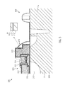
- FIG. 5 illustrates in some detail a semiconductor device 300 comprising a memory device 310 formed in and on a flash memory area F of a semiconductor layer 330 and a FET 320 formed in and on a logic area L of the semiconductor layer 330 .
- the memory device 310 comprises a control gate 311 formed over a floating gate 312 and separated therefrom by an ONO layer 313 . Moreover, the memory device 310 comprises an erase gate 314 and a select gate 315 formed to partially overlap the control gate 311 .
- the memory device 310 comprises an isolation structure 316 that might partially be formed during the process of forming sidewall spacers of the FET device 320 .
- a metal layer 317 may be formed between the floating gate layer and the insulation layer, as illustrated in the expanded view.
- an array of memory cells each arranged in rows and columns and each comprising a split gate memory device may be formed. Moreover, columns of memory cells separated by columns of isolation regions in an interlaced fashion may be formed. Each column of memory cells may contain a pair of the memory devices as the ones shown over and in logic areas of a wafer in FIGS. 3 f and 4 e and each pair of memory devices may share the same source region and adjacent pairs may share the same drain region. Select gates for an entire row of memory cells may be formed as a single conductive word line, such that each word line forms a select gate for one of the memory devices in each column of the memory cells (e each word line electrically connects together a row of the select gates).
- Control gates may be similarly formed as a continuous control gate line extending along the row of memory cells (i.e., electrically connecting together a row of the control gates), and the erase gates may also be formed as a continuous erase gate line extending along the row of memory cells (i.e., electrically connecting together a row of the erase gates.
- the present disclosure provides techniques for the integration of the formation of a split gate memory device in the HKMG first manufacturing of HKMG FETs.
- the manufacturing of reliably operating semiconductor devices comprising memory cells and logic devices may be significantly improved as compared to the art.
Landscapes
- Engineering & Computer Science (AREA)
- Microelectronics & Electronic Packaging (AREA)
- Power Engineering (AREA)
- Physics & Mathematics (AREA)
- Condensed Matter Physics & Semiconductors (AREA)
- General Physics & Mathematics (AREA)
- Computer Hardware Design (AREA)
- Ceramic Engineering (AREA)
- Manufacturing & Machinery (AREA)
- Non-Volatile Memory (AREA)
- Semiconductor Memories (AREA)
Abstract
Description
Claims (20)
Priority Applications (1)
| Application Number | Priority Date | Filing Date | Title |
|---|---|---|---|
| US14/982,228 US9754951B2 (en) | 2015-10-30 | 2015-12-29 | Semiconductor device with a memory device and a high-K metal gate transistor |
Applications Claiming Priority (2)
| Application Number | Priority Date | Filing Date | Title |
|---|---|---|---|
| US201562248723P | 2015-10-30 | 2015-10-30 | |
| US14/982,228 US9754951B2 (en) | 2015-10-30 | 2015-12-29 | Semiconductor device with a memory device and a high-K metal gate transistor |
Publications (2)
| Publication Number | Publication Date |
|---|---|
| US20170125432A1 US20170125432A1 (en) | 2017-05-04 |
| US9754951B2 true US9754951B2 (en) | 2017-09-05 |
Family
ID=58638316
Family Applications (1)
| Application Number | Title | Priority Date | Filing Date |
|---|---|---|---|
| US14/982,228 Active 2036-01-02 US9754951B2 (en) | 2015-10-30 | 2015-12-29 | Semiconductor device with a memory device and a high-K metal gate transistor |
Country Status (1)
| Country | Link |
|---|---|
| US (1) | US9754951B2 (en) |
Cited By (1)
| Publication number | Priority date | Publication date | Assignee | Title |
|---|---|---|---|---|
| US11631772B2 (en) | 2021-01-13 | 2023-04-18 | Globalfoundries U.S. Inc. | Non-volatile memory structure using semiconductor layer as floating gate and bulk semiconductor substrate as channel region |
Families Citing this family (6)
| Publication number | Priority date | Publication date | Assignee | Title |
|---|---|---|---|---|
| CN107305892B (en) * | 2016-04-20 | 2020-10-02 | 硅存储技术公司 | Method of forming tri-gate non-volatile flash memory cell pairs using two polysilicon deposition steps |
| US9929167B2 (en) | 2016-07-13 | 2018-03-27 | Taiwan Semiconductor Manufacturing Co., Ltd. | Semiconductor device and manufacturing method thereof |
| US10347728B1 (en) * | 2018-01-02 | 2019-07-09 | Microchip Technology Incorporated | Memory cell with asymmetric word line and erase gate for decoupled program erase performance |
| US11380769B2 (en) * | 2019-10-01 | 2022-07-05 | Taiwan Semiconductor Manufacturing Company, Ltd. | Select gate spacer formation to facilitate embedding of split gate flash memory |
| KR20230001802A (en) * | 2021-06-29 | 2023-01-05 | 삼성전자주식회사 | Integrated circuit device |
| CN114335004B (en) * | 2022-03-11 | 2022-05-17 | 江苏游隼微电子有限公司 | 1.5T SONOS device and preparation method thereof |
Citations (8)
| Publication number | Priority date | Publication date | Assignee | Title |
|---|---|---|---|---|
| US20050087892A1 (en) | 2003-10-27 | 2005-04-28 | Cheng-Yuan Hsu | [nand flash memory cell row, nand flash memory cell array, operation and fabrication method thereof] |
| US20070241386A1 (en) * | 2006-04-13 | 2007-10-18 | Shih Wei Wang | Method for reducing topography of non-volatile memory and resulting memory cells |
| US20150035040A1 (en) * | 2013-08-02 | 2015-02-05 | Silicon Storage Technology, Inc. | Split Gate Non-volatile Flash Memory Cell Having A Silicon-Metal Floating Gate And Method Of Making Same |
| US20150054044A1 (en) * | 2013-08-22 | 2015-02-26 | Freescale Semiconductor, Inc | Method to Form a Polysilicon Nanocrystal Thin Film Storage Bitcell within a High K Metal Gate Platform Technology Using a Gate Last Process to Form Transistor Gates |
| US20150123186A1 (en) * | 2012-10-31 | 2015-05-07 | Hewlett-Packard Development Company, L.P. | Memory cell that prevents charge loss |
| US20150187780A1 (en) * | 2013-12-30 | 2015-07-02 | Semiconductor Manufacturing International (Shanghai) Corporation | Memory device and method for forming the same |
| US20150263040A1 (en) * | 2014-03-17 | 2015-09-17 | Silicon Storage Technology, Inc. | Embedded Memory Device With Silicon-On-Insulator Substrate, And Method Of Making Same |
| US20160163722A1 (en) | 2014-12-04 | 2016-06-09 | United Microelectronics Corp. | Non-volatile memory cell and method of manufacturing the same |
-
2015
- 2015-12-29 US US14/982,228 patent/US9754951B2/en active Active
Patent Citations (8)
| Publication number | Priority date | Publication date | Assignee | Title |
|---|---|---|---|---|
| US20050087892A1 (en) | 2003-10-27 | 2005-04-28 | Cheng-Yuan Hsu | [nand flash memory cell row, nand flash memory cell array, operation and fabrication method thereof] |
| US20070241386A1 (en) * | 2006-04-13 | 2007-10-18 | Shih Wei Wang | Method for reducing topography of non-volatile memory and resulting memory cells |
| US20150123186A1 (en) * | 2012-10-31 | 2015-05-07 | Hewlett-Packard Development Company, L.P. | Memory cell that prevents charge loss |
| US20150035040A1 (en) * | 2013-08-02 | 2015-02-05 | Silicon Storage Technology, Inc. | Split Gate Non-volatile Flash Memory Cell Having A Silicon-Metal Floating Gate And Method Of Making Same |
| US20150054044A1 (en) * | 2013-08-22 | 2015-02-26 | Freescale Semiconductor, Inc | Method to Form a Polysilicon Nanocrystal Thin Film Storage Bitcell within a High K Metal Gate Platform Technology Using a Gate Last Process to Form Transistor Gates |
| US20150187780A1 (en) * | 2013-12-30 | 2015-07-02 | Semiconductor Manufacturing International (Shanghai) Corporation | Memory device and method for forming the same |
| US20150263040A1 (en) * | 2014-03-17 | 2015-09-17 | Silicon Storage Technology, Inc. | Embedded Memory Device With Silicon-On-Insulator Substrate, And Method Of Making Same |
| US20160163722A1 (en) | 2014-12-04 | 2016-06-09 | United Microelectronics Corp. | Non-volatile memory cell and method of manufacturing the same |
Non-Patent Citations (1)
| Title |
|---|
| Office Action from related U.S. Appl. No. 15/140,616 dated Sep. 12, 2016. |
Cited By (1)
| Publication number | Priority date | Publication date | Assignee | Title |
|---|---|---|---|---|
| US11631772B2 (en) | 2021-01-13 | 2023-04-18 | Globalfoundries U.S. Inc. | Non-volatile memory structure using semiconductor layer as floating gate and bulk semiconductor substrate as channel region |
Also Published As
| Publication number | Publication date |
|---|---|
| US20170125432A1 (en) | 2017-05-04 |
Similar Documents
| Publication | Publication Date | Title |
|---|---|---|
| US9754951B2 (en) | Semiconductor device with a memory device and a high-K metal gate transistor | |
| US8399310B2 (en) | Non-volatile memory and logic circuit process integration | |
| EP2725607B1 (en) | Method of making a logic transistor and a non-volatile memory (nvm) cell | |
| US8389365B2 (en) | Non-volatile memory and logic circuit process integration | |
| US8564044B2 (en) | Non-volatile memory and logic circuit process integration | |
| US9871050B1 (en) | Flash memory device | |
| US10529728B2 (en) | Semiconductor structure including a plurality of pairs of nonvolatile memory cells and an edge cell | |
| US20170236833A1 (en) | Hkmg high voltage cmos for embedded non-volatile memory | |
| US9368605B2 (en) | Semiconductor structure including a split gate nonvolatile memory cell and a high voltage transistor, and method for the formation thereof | |
| CN108878427B (en) | Semiconductor device and method for manufacturing the same | |
| US9673210B1 (en) | Semiconductor structure including a nonvolatile memory cell having a charge trapping layer and method for the formation thereof | |
| US9831262B2 (en) | Embedded HKMG non-volatile memory | |
| US10032891B2 (en) | FinFET based flash memory cell | |
| US10811424B2 (en) | Integrated computing structures formed on silicon | |
| US9972634B2 (en) | Semiconductor device comprising a floating gate flash memory device | |
| CN107437507B (en) | SOI memory device | |
| US9793286B2 (en) | Embedded HKMG non-volatile memory | |
| US11600628B2 (en) | Floating gate memory cell and memory array structure |
Legal Events
| Date | Code | Title | Description |
|---|---|---|---|
| AS | Assignment |
Owner name: GLOBALFOUNDRIES INC., CAYMAN ISLANDS Free format text: ASSIGNMENT OF ASSIGNORS INTEREST;ASSIGNORS:RICHTER, RALF;BEYER, SVEN;SIGNING DATES FROM 20151214 TO 20151215;REEL/FRAME:037374/0106 |
|
| STCF | Information on status: patent grant |
Free format text: PATENTED CASE |
|
| AS | Assignment |
Owner name: WILMINGTON TRUST, NATIONAL ASSOCIATION, DELAWARE Free format text: SECURITY AGREEMENT;ASSIGNOR:GLOBALFOUNDRIES INC.;REEL/FRAME:049490/0001 Effective date: 20181127 |
|
| MAFP | Maintenance fee payment |
Free format text: PAYMENT OF MAINTENANCE FEE, 4TH YEAR, LARGE ENTITY (ORIGINAL EVENT CODE: M1551); ENTITY STATUS OF PATENT OWNER: LARGE ENTITY Year of fee payment: 4 |
|
| AS | Assignment |
Owner name: GLOBALFOUNDRIES U.S. INC., CALIFORNIA Free format text: ASSIGNMENT OF ASSIGNORS INTEREST;ASSIGNOR:GLOBALFOUNDRIES INC.;REEL/FRAME:054633/0001 Effective date: 20201022 |
|
| AS | Assignment |
Owner name: GLOBALFOUNDRIES INC., CAYMAN ISLANDS Free format text: RELEASE BY SECURED PARTY;ASSIGNOR:WILMINGTON TRUST, NATIONAL ASSOCIATION;REEL/FRAME:054636/0001 Effective date: 20201117 |
|
| AS | Assignment |
Owner name: GLOBALFOUNDRIES U.S. INC., NEW YORK Free format text: RELEASE BY SECURED PARTY;ASSIGNOR:WILMINGTON TRUST, NATIONAL ASSOCIATION;REEL/FRAME:056987/0001 Effective date: 20201117 |